Embed Size (px)
Citation preview
DAQ S SeriesNI 6124/6154 User ManualDAQ-STC2 S Series Simultaneous Sampling Multifunction Input/Output Devices
NI 6124/6154 User Manual
August 2008372613A-01
Support
Worldwide Technical Support and Product Information
ni.com
National Instruments Corporate Headquarters
11500 North Mopac Expressway Austin, Texas 78759-3504 USA Tel: 512 683 0100
Worldwide Offices
Australia 1800 300 800, Austria 43 662 457990-0, Belgium 32 (0) 2 757 0020, Brazil 55 11 3262 3599, Canada 800 433 3488, China 86 21 5050 9800, Czech Republic 420 224 235 774, Denmark 45 45 76 26 00, Finland 358 (0) 9 725 72511, France 01 57 66 24 24, Germany 49 89 7413130, India 91 80 41190000, Israel 972 3 6393737, Italy 39 02 41309277, Japan 0120-527196, Korea 82 02 3451 3400, Lebanon 961 (0) 1 33 28 28, Malaysia 1800 887710, Mexico 01 800 010 0793, Netherlands 31 (0) 348 433 466, New Zealand 0800 553 322, Norway 47 (0) 66 90 76 60, Poland 48 22 3390150, Portugal 351 210 311 210, Russia 7 495 783 6851, Singapore 1800 226 5886, Slovenia 386 3 425 42 00, South Africa 27 0 11 805 8197, Spain 34 91 640 0085, Sweden 46 (0) 8 587 895 00, Switzerland 41 56 2005151, Taiwan 886 02 2377 2222, Thailand 662 278 6777, Turkey 90 212 279 3031, United Kingdom 44 (0) 1635 523545
For further support information, refer to the Technical Support and Professional Services appendix. To comment on National Instruments documentation, refer to the National Instruments Web site at ni.com/info and enter the info code feedback.
© 2008 National Instruments Corporation. All rights reserved.
Important Information
WarrantyNI 6124 and NI 6154 devices are warranted against defects in materials and workmanship for a period of one year from the date of shipment, as evidenced by receipts or other documentation. National Instruments will, at its option, repair or replace equipment that proves to be defective during the warranty period. This warranty includes parts and labor.
The media on which you receive National Instruments software are warranted not to fail to execute programming instructions, due to defects in materials and workmanship, for a period of 90 days from date of shipment, as evidenced by receipts or other documentation. National Instruments will, at its option, repair or replace software media that do not execute programming instructions if National Instruments receives notice of such defects during the warranty period. National Instruments does not warrant that the operation of the software shall be uninterrupted or error free.
A Return Material Authorization (RMA) number must be obtained from the factory and clearly marked on the outside of the package before any equipment will be accepted for warranty work. National Instruments will pay the shipping costs of returning to the owner parts which are covered by warranty.
National Instruments believes that the information in this document is accurate. The document has been carefully reviewed for technical accuracy. In the event that technical or typographical errors exist, National Instruments reserves the right to make changes to subsequent editions of this document without prior notice to holders of this edition. The reader should consult National Instruments if errors are suspected. In no event shall National Instruments be liable for any damages arising out of or related to this document or the information contained in it.
EXCEPT AS SPECIFIED HEREIN, NATIONAL INSTRUMENTS MAKES NO WARRANTIES, EXPRESS OR IMPLIED, AND SPECIFICALLY DISCLAIMS ANY WARRANTY OF MERCHANTABILITY OR FITNESS FOR A PARTICULAR PURPOSE. CUSTOMER’S RIGHT TO RECOVER DAMAGES CAUSED BY FAULT OR NEGLIGENCE ON THE PART OF NATIONAL INSTRUMENTS SHALL BE LIMITED TO THE AMOUNT THERETOFORE PAID BY THE CUSTOMER. NATIONAL INSTRUMENTS WILL NOT BE LIABLE FOR DAMAGES RESULTING FROM LOSS OF DATA, PROFITS, USE OF PRODUCTS, OR INCIDENTAL OR CONSEQUENTIAL DAMAGES, EVEN IF ADVISED OF THE POSSIBILITY THEREOF. This limitation of the liability of National Instruments will apply regardless of the form of action, whether in contract or tort, including negligence. Any action against National Instruments must be brought within one year after the cause of action accrues. National Instruments shall not be liable for any delay in performance due to causes beyond its reasonable control. The warranty provided herein does not cover damages, defects, malfunctions, or service failures caused by owner’s failure to follow the National Instruments installation, operation, or maintenance instructions; owner’s modification of the product; owner’s abuse, misuse, or negligent acts; and power failure or surges, fire, flood, accident, actions of third parties, or other events outside reasonable control.
CopyrightUnder the copyright laws, this publication may not be reproduced or transmitted in any form, electronic or mechanical, including photocopying, recording, storing in an information retrieval system, or translating, in whole or in part, without the prior written consent of National Instruments Corporation.
National Instruments respects the intellectual property of others, and we ask our users to do the same. NI software is protected by copyright and other intellectual property laws. Where NI software may be used to reproduce software or other materials belonging to others, you may use NI software only to reproduce materials that you may reproduce in accordance with the terms of any applicable license or other legal restriction.
TrademarksNational Instruments, NI, ni.com, and LabVIEW are trademarks of National Instruments Corporation. Refer to the Terms of Use section on ni.com/legal for more information about National Instruments trademarks.
Other product and company names mentioned herein are trademarks or trade names of their respective companies.
Members of the National Instruments Alliance Partner Program are business entities independent from National Instruments and have no agency, partnership, or joint-venture relationship with National Instruments.
PatentsFor patents covering National Instruments products/technology, refer to the appropriate location: Help»Patents in your software, the patents.txt file on your media, or the National Instruments Patent Notice at ni.com/patents.
WARNING REGARDING USE OF NATIONAL INSTRUMENTS PRODUCTS(1) NATIONAL INSTRUMENTS PRODUCTS ARE NOT DESIGNED WITH COMPONENTS AND TESTING FOR A LEVEL OF RELIABILITY SUITABLE FOR USE IN OR IN CONNECTION WITH SURGICAL IMPLANTS OR AS CRITICAL COMPONENTS IN ANY LIFE SUPPORT SYSTEMS WHOSE FAILURE TO PERFORM CAN REASONABLY BE EXPECTED TO CAUSE SIGNIFICANT INJURY TO A HUMAN.
(2) IN ANY APPLICATION, INCLUDING THE ABOVE, RELIABILITY OF OPERATION OF THE SOFTWARE PRODUCTS CAN BE IMPAIRED BY ADVERSE FACTORS, INCLUDING BUT NOT LIMITED TO FLUCTUATIONS IN ELECTRICAL POWER SUPPLY, COMPUTER HARDWARE MALFUNCTIONS, COMPUTER OPERATING SYSTEM SOFTWARE FITNESS, FITNESS OF COMPILERS AND DEVELOPMENT SOFTWARE USED TO DEVELOP AN APPLICATION, INSTALLATION ERRORS, SOFTWARE AND HARDWARE COMPATIBILITY PROBLEMS, MALFUNCTIONS OR FAILURES OF ELECTRONIC MONITORING OR CONTROL DEVICES, TRANSIENT FAILURES OF ELECTRONIC SYSTEMS (HARDWARE AND/OR SOFTWARE), UNANTICIPATED USES OR MISUSES, OR ERRORS ON THE PART OF THE USER OR APPLICATIONS DESIGNER (ADVERSE FACTORS SUCH AS THESE ARE HEREAFTER COLLECTIVELY TERMED “SYSTEM FAILURES”). ANY APPLICATION WHERE A SYSTEM FAILURE WOULD CREATE A RISK OF HARM TO PROPERTY OR PERSONS (INCLUDING THE RISK OF BODILY INJURY AND DEATH) SHOULD NOT BE RELIANT SOLELY UPON ONE FORM OF ELECTRONIC SYSTEM DUE TO THE RISK OF SYSTEM FAILURE. TO AVOID DAMAGE, INJURY, OR DEATH, THE USER OR APPLICATION DESIGNER MUST TAKE REASONABLY PRUDENT STEPS TO PROTECT AGAINST SYSTEM FAILURES, INCLUDING BUT NOT LIMITED TO BACK-UP OR SHUT DOWN MECHANISMS. BECAUSE EACH END-USER SYSTEM IS CUSTOMIZED AND DIFFERS FROM NATIONAL INSTRUMENTS' TESTING PLATFORMS AND BECAUSE A USER OR APPLICATION DESIGNER MAY USE NATIONAL INSTRUMENTS PRODUCTS IN COMBINATION WITH OTHER PRODUCTS IN A MANNER NOT EVALUATED OR CONTEMPLATED BY NATIONAL INSTRUMENTS, THE USER OR APPLICATION DESIGNER IS ULTIMATELY RESPONSIBLE FOR VERIFYING AND VALIDATING THE SUITABILITY OF NATIONAL INSTRUMENTS PRODUCTS WHENEVER NATIONAL INSTRUMENTS PRODUCTS ARE INCORPORATED IN A SYSTEM OR APPLICATION, INCLUDING, WITHOUT LIMITATION, THE APPROPRIATE DESIGN, PROCESS AND SAFETY LEVEL OF SUCH SYSTEM OR APPLICATION.
Compliance
Compliance with FCC/Canada Radio Frequency Interference Regulations
Determining FCC ClassThe Federal Communications Commission (FCC) has rules to protect wireless communications from interference. The FCC places digital electronics into two classes. These classes are known as Class A (for use in industrial-commercial locations only) or Class B (for use in residential or commercial locations). All National Instruments (NI) products are FCC Class A products.Depending on where it is operated, this Class A product could be subject to restrictions in the FCC rules. (In Canada, the Department of Communications (DOC), of Industry Canada, regulates wireless interference in much the same way.) Digital electronics emit weak signals during normal operation that can affect radio, television, or other wireless products.All Class A products display a simple warning statement of one paragraph in length regarding interference and undesired operation. The FCC rules have restrictions regarding the locations where FCC Class A products can be operated.Consult the FCC Web site at www.fcc.gov for more information.
FCC/DOC WarningsThis equipment generates and uses radio frequency energy and, if not installed and used in strict accordance with the instructions in this manual and the CE marking Declaration of Conformity*, may cause interference to radio and television reception. Classification requirements are the same for the Federal Communications Commission (FCC) and the Canadian Department of Communications (DOC). Changes or modifications not expressly approved by NI could void the user’s authority to operate the equipment under the FCC Rules.
Class AFederal Communications CommissionThis equipment has been tested and found to comply with the limits for a Class A digital device, pursuant to part 15 of the FCC Rules. These limits are designed to provide reasonable protection against harmful interference when the equipment is operated in a commercial environment. This equipment generates, uses, and can radiate radio frequency energy and, if not installed and used in accordance with the instruction manual, may cause harmful interference to radio communications. Operation of this equipment in a residential area is likely to cause harmful interference in which case the user is required to correct the interference at their own expense.
Canadian Department of CommunicationsThis Class A digital apparatus meets all requirements of the Canadian Interference-Causing Equipment Regulations.Cet appareil numérique de la classe A respecte toutes les exigences du Règlement sur le matériel brouilleur du Canada.
Compliance with EU DirectivesUsers in the European Union (EU) should refer to the Declaration of Conformity (DoC) for information* pertaining to the CE marking. Refer to the Declaration of Conformity (DoC) for this product for any additional regulatory compliance information. To obtain the DoC for this product, visit ni.com/certification, search by model number or product line, and click the appropriate link in the Certification column.
* The CE marking Declaration of Conformity contains important supplementary information and instructions for the user or installer.
© National Instruments Corporation v NI 6124/6154 User Manual
Contents
About This ManualConventions ...................................................................................................................xiRelated Documentation..................................................................................................xii
Chapter 1Getting Started
Installing NI-DAQmx ....................................................................................................1-1Installing Other Software...............................................................................................1-1Installing the Hardware..................................................................................................1-2Device Self-Calibration .................................................................................................1-2Device Pinouts ...............................................................................................................1-3Device Specifications ....................................................................................................1-3
Chapter 2DAQ System Overview
DAQ Hardware ..............................................................................................................2-2DAQ-STC2......................................................................................................2-3
Calibration Circuitry ......................................................................................................2-4Internal or Self-Calibration..............................................................................2-4External Calibration.........................................................................................2-5
Signal Conditioning .......................................................................................................2-5Sensors and Transducers................................................................................................2-5Programming Devices in Software ................................................................................2-6
Chapter 3I/O Connector
NI 6124 I/O Connector Signal Descriptions..................................................................3-1NI 6154 I/O Connector Signal Descriptions..................................................................3-2+5 V Power Source ........................................................................................................3-3
Chapter 4Analog Input
Analog Input Terminal Configuration ...........................................................................4-2Input Polarity and Range ...............................................................................................4-3Working Voltage Range ................................................................................................4-4AI Data Acquisition Methods ........................................................................................4-4Analog Input Triggering ................................................................................................4-6
Contents
NI 6124/6154 User Manual vi ni.com
Connecting Analog Input Signals.................................................................................. 4-6Types of Signal Sources.................................................................................. 4-7Differential Connections for Ground-Referenced Signal Sources.................. 4-7
Common-Mode Signal Rejection Considerations ............................ 4-9Differential Connections for Non-Referenced or Floating Signal Sources .... 4-9
DC-Coupled...................................................................................... 4-10AC-Coupled...................................................................................... 4-11
Field Wiring Considerations ........................................................................... 4-11Minimizing Drift in Differential Mode........................................................... 4-12
Analog Input Timing Signals ........................................................................................ 4-13AI Sample Clock Signal.................................................................................. 4-14
Using an Internal Source .................................................................. 4-14Using an External Source ................................................................. 4-15Routing AI Sample Clock Signal to an Output Terminal................. 4-15Other Timing Requirements ............................................................. 4-15
AI Sample Clock Timebase Signal ................................................................. 4-16AI Convert Clock Signal................................................................................. 4-16
Using an Internal Source .................................................................. 4-17Using an External Source ................................................................. 4-17Routing AI Convert Clock Signal to an Output Terminal................ 4-17
AI Convert Clock Timebase Signal ................................................................ 4-17AI Hold Complete Event Signal ..................................................................... 4-18AI Start Trigger Signal.................................................................................... 4-18
Using a Digital Source...................................................................... 4-18Using an Analog Source ................................................................... 4-19Routing AI Start Trigger to an Output Terminal .............................. 4-19
AI Reference Trigger Signal ........................................................................... 4-19Using a Digital Source...................................................................... 4-20Using an Analog Source ................................................................... 4-20Routing AI Reference Trigger Signal to an Output Terminal .......... 4-20
Getting Started with AI Applications in Software ........................................................ 4-21
Chapter 5Analog Output
Minimizing Glitches on the Output Signal.................................................................... 5-2AO Data Generation Methods ....................................................................................... 5-2Analog Output Triggering ............................................................................................. 5-4Connecting Analog Output Signals ............................................................................... 5-4Waveform Generation Timing Signals.......................................................................... 5-6
AO Sample Clock Signal ................................................................................ 5-6Using an Internal Source .................................................................. 5-6Using an External Source ................................................................. 5-7Routing AO Sample Clock Signal to an Output Terminal ............... 5-7
Contents
© National Instruments Corporation vii NI 6124/6154 User Manual
Other Timing Requirements..............................................................5-7AO Sample Clock Timebase Signal ................................................................5-8AO Start Trigger Signal...................................................................................5-9
Using a Digital Source ......................................................................5-9Using an Analog Source ...................................................................5-10Routing AO Start Trigger Signal to an Output Terminal..................5-10
AO Pause Trigger Signal.................................................................................5-10Using a Digital Source ......................................................................5-11Using an Analog Source ...................................................................5-11
Getting Started with AO Applications in Software .......................................................5-11
Chapter 6Digital I/O
Digital I/O for Non-Isolated Devices.............................................................................6-1Static DIO for Non-Isolated Devices ..............................................................6-2Digital Waveform Triggering for Non-Isolated Devices ................................6-3Digital Waveform Acquisition for Non-Isolated Devices...............................6-3
DI Sample Clock Signal....................................................................6-4Digital Waveform Generation for Non-Isolated Devices................................6-5
DO Sample Clock Signal ..................................................................6-5I/O Protection for Non-Isolated Devices.........................................................6-7Programmable Power-Up States for Non-Isolated Devices ............................6-7DI Change Detection for Non-Isolated Devices..............................................6-8
DI Change Detection Applications for Non-Isolated Devices..........6-9Connecting Digital I/O Signals on Non-Isolated Devices...............................6-9Getting Started with DIO Applications in Software on Non-Isolated Devices .....6-10
Digital I/O for Isolated Devices.....................................................................................6-11Static DIO for Isolated Devices.......................................................................6-11I/O Protection for Isolated Devices .................................................................6-12Connecting Digital I/O Signals on Isolated Devices.......................................6-12Getting Started with DIO Applications in Software on Isolated Devices .......6-13
Chapter 7Counters
Counter Input Applications............................................................................................7-2Counting Edges ...............................................................................................7-2
Single Point (On-Demand) Edge Counting ......................................7-2Buffered (Sample Clock) Edge Counting .........................................7-3Controlling the Direction of Counting ..............................................7-4
Pulse-Width Measurement ..............................................................................7-4Single Pulse-Width Measurement.....................................................7-4Buffered Pulse-Width Measurement.................................................7-5
Contents
NI 6124/6154 User Manual viii ni.com
Period Measurement ....................................................................................... 7-6Single Period Measurement.............................................................. 7-6Buffered Period Measurement.......................................................... 7-7
Semi-Period Measurement .............................................................................. 7-7Single Semi-Period Measurement .................................................... 7-8Buffered Semi-Period Measurement ................................................ 7-8
Frequency Measurement ................................................................................. 7-9Choosing a Method for Measuring Frequency ................................. 7-12
Position Measurement..................................................................................... 7-14Measurements Using Quadrature Encoders...................................... 7-14Measurements Using Two Pulse Encoders ...................................... 7-16Buffered (Sample Clock) Position Measurement ............................. 7-17
Two-Signal Edge-Separation Measurement ................................................... 7-17Single Two-Signal Edge-Separation Measurement.......................... 7-18Buffered Two-Signal Edge-Separation Measurement...................... 7-18
Counter Output Applications......................................................................................... 7-19Simple Pulse Generation................................................................................. 7-19
Single Pulse Generation.................................................................... 7-19Single Pulse Generation with Start Trigger ...................................... 7-20Retriggerable Single Pulse Generation............................................. 7-20
Pulse Train Generation.................................................................................... 7-21Continuous Pulse Train Generation.................................................. 7-21Finite Pulse Train Generation........................................................... 7-22
Frequency Generation ..................................................................................... 7-23Using the Frequency Generator ........................................................ 7-23
Frequency Division ......................................................................................... 7-24Pulse Generation for ETS ............................................................................... 7-24
Counter Timing Signals................................................................................................. 7-25Counter n Source Signal ................................................................................. 7-26
Routing a Signal to Counter n Source .............................................. 7-26Routing Counter n Source to an Output Terminal............................ 7-27
Counter n Gate Signal ..................................................................................... 7-27Routing a Signal to Counter n Gate.................................................. 7-27Routing Counter n Gate to an Output Terminal ............................... 7-27
Counter n Aux Signal...................................................................................... 7-28Routing a Signal to Counter n Aux .................................................. 7-28
Counter n A, Counter n B, and Counter n Z Signals ...................................... 7-28Routing Signals to A, B, and Z Counter Inputs................................ 7-28Routing Counter n Z Signal to an Output Terminal ......................... 7-28
Counter n Up_Down Signal ............................................................................ 7-29Counter n HW Arm Signal.............................................................................. 7-29
Routing Signals to Counter n HW Arm Input .................................. 7-29Counter n Internal Output and Counter n TC Signals..................................... 7-29
Routing Counter n Internal Output to an Output Terminal .............. 7-30
Contents
© National Instruments Corporation ix NI 6124/6154 User Manual
Frequency Output Signal.................................................................................7-30Routing Frequency Output to a Terminal .........................................7-30
Default Counter/Timer Pinouts......................................................................................7-30Counter Triggering ........................................................................................................7-31Other Counter Features ..................................................................................................7-32
Cascading Counters .........................................................................................7-32Counter Filters .................................................................................................7-32Prescaling ........................................................................................................7-33Duplicate Count Prevention ............................................................................7-34
Example Application That Works Correctly (No Duplicate Counting) ... 7-35Example Application That Works Incorrectly (Duplicate Counting) ....7-36Example Application That Prevents Duplicate Count ......................7-36When To Use Duplicate Count Prevention.......................................7-37Enabling Duplicate Count Prevention in NI-DAQmx ......................7-37
Synchronization Modes ...................................................................................7-3780 MHz Source Mode .......................................................................7-38Other Internal Source Mode..............................................................7-39External Source Mode.......................................................................7-39
Chapter 8Programmable Function Interfaces (PFI)
PFI for Non-Isolated Devices ........................................................................................8-1PFI for Isolated Devices ................................................................................................8-2Using PFI Terminals as Timing Input Signals...............................................................8-4Exporting Timing Output Signals Using PFI Terminals ...............................................8-4Using PFI Terminals as Static Digital Inputs and Outputs ............................................8-5Connecting PFI Input Signals ........................................................................................8-6PFI Filters ......................................................................................................................8-6I/O Protection.................................................................................................................8-8Programmable Power-Up States ....................................................................................8-8
Chapter 9Digital Routing and Clock Generation
Clock Routing ................................................................................................................9-180 MHz Timebase ...........................................................................................9-220 MHz Timebase ...........................................................................................9-2100 kHz Timebase...........................................................................................9-2External Reference Clock................................................................................9-210 MHz Reference Clock ................................................................................9-3
Synchronizing Multiple Devices ...................................................................................9-3
Contents
NI 6124/6154 User Manual x ni.com
Real-Time System Integration (RTSI) .......................................................................... 9-4RTSI Connector Pinout ................................................................................... 9-4Using RTSI as Outputs ................................................................................... 9-5Using RTSI Terminals as Timing Input Signals ............................................. 9-6RTSI Filters..................................................................................................... 9-6
PXI Clock and Trigger Signals...................................................................................... 9-8PXI_CLK10 .................................................................................................... 9-8PXI Triggers.................................................................................................... 9-8PXI_STAR Trigger ......................................................................................... 9-8PXI_STAR Filters........................................................................................... 9-9
Routing Signals in Software.......................................................................................... 9-10
Chapter 10Bus Interface
MITE and DAQ-PnP ..................................................................................................... 10-1PXI Considerations........................................................................................................ 10-1
PXI Clock and Trigger Signals ....................................................................... 10-1PXI Express..................................................................................................... 10-1
Data Transfer Methods .................................................................................................. 10-2Changing Data Transfer Methods between DMA and IRQ............................ 10-2
Chapter 11Triggering
Triggering with a Digital Source................................................................................... 11-1Triggering with an Analog Source ................................................................................ 11-2
Analog Input Channel ..................................................................................... 11-3Analog Trigger Actions .................................................................................. 11-3
Analog Trigger Types.................................................................................................... 11-3Analog Trigger Accuracy .............................................................................................. 11-6
Appendix ADevice-Specific Information
Appendix BTechnical Support and Professional Services
Glossary
Index
© National Instruments Corporation xi NI 6124/6154 User Manual
About This Manual
The NI 6124/6154 User Manual contains information about using the National Instruments S Series NI 6124 and NI 6154 data acquisition (DAQ) devices with NI-DAQmx 8.8 and later.
ConventionsThe following conventions appear in this manual:
<> Angle brackets that contain numbers separated by an ellipsis represent a range of values associated with a bit or signal name—for example, AO <3..0>.
» The » symbol leads you through nested menu items and dialog box options to a final action. The sequence File»Page Setup»Options directs you to pull down the File menu, select the Page Setup item, and select Options from the last dialog box.
This icon denotes a note, which alerts you to important information.
This icon denotes a caution, which advises you of precautions to take to avoid injury, data loss, or a system crash. When this symbol is marked on a product, refer to the Read Me First: Safety and Radio-Frequency Interference document for information about precautions to take.
bold Bold text denotes items that you must select or click in the software, such as menu items and dialog box options. Bold text also denotes parameter names.
italic Italic text denotes variables, emphasis, a cross-reference, or an introduction to a key concept. Italic text also denotes text that is a placeholder for a word or value that you must supply.
monospace Text in this font denotes text or characters that you should enter from the keyboard, sections of code, programming examples, and syntax examples. This font is also used for the proper names of disk drives, paths, directories, programs, subprograms, subroutines, device names, functions, operations, variables, filenames, and extensions.
Platform Text in this font denotes a specific platform and indicates that the text following it applies only to that platform.
About This Manual
NI 6124/6154 User Manual xii ni.com
Related DocumentationEach application software package and driver includes information about writing applications for taking measurements and controlling measurement devices. The following references to documents assume you have NI-DAQmx 8.8 or later, and where applicable, version 7.1 or later of the NI application software.
NI-DAQmx for WindowsThe DAQ Getting Started Guide describes how to install your NI-DAQmx for Windows software, how to install your NI-DAQmx-supported DAQ device, and how to confirm that your device is operating properly. Select Start»All Programs»National Instruments»NI-DAQ»DAQ Getting Started Guide.
The NI-DAQ Readme lists which devices are supported by this version of NI-DAQmx. Select Start»All Programs»National Instruments»NI-DAQ»NI-DAQ Readme.
The NI-DAQmx Help contains general information about measurement concepts, key NI-DAQmx concepts, and common applications that are applicable to all programming environments. Select Start»All Programs»National Instruments»NI-DAQ»NI-DAQmx Help.
LabVIEWIf you are a new user, use the Getting Started with LabVIEW manual to familiarize yourself with the LabVIEW graphical programming environment and the basic LabVIEW features you use to build data acquisition and instrument control applications. Open the Getting Started with LabVIEW manual by selecting Start»All Programs»National Instruments»LabVIEW»LabVIEW Manuals or by navigating to the labview\manuals directory and opening LV_Getting_Started.pdf.
Use the LabVIEW Help, available by selecting Help»Search the LabVIEW Help in LabVIEW, to access information about LabVIEW programming concepts, step-by-step instructions for using LabVIEW, and reference information about LabVIEW VIs, functions, palettes, menus, and tools. Refer to the following locations on the Contents tab of the LabVIEW Help for information about NI-DAQmx:
• Getting Started with LabVIEW»Getting Started with DAQ— Includes overview information and a tutorial to learn how to take an NI-DAQmx measurement in LabVIEW using the DAQ Assistant.
About This Manual
© National Instruments Corporation xiii NI 6124/6154 User Manual
• VI and Function Reference»Measurement I/O VIs and Functions—Describes the LabVIEW NI-DAQmx VIs and properties.
• Taking Measurements—Contains the conceptual and how-to information you need to acquire and analyze measurement data in LabVIEW, including common measurements, measurement fundamentals, NI-DAQmx key concepts, and device considerations.
LabWindows/CVIThe Data Acquisition book of the LabWindows/CVI Help contains measurement concepts for NI-DAQmx. This book also contains Taking an NI-DAQmx Measurement in LabWindows/CVI, which includes step-by-step instructions about creating a measurement task using the DAQ Assistant. In LabWindows™/CVI™, select Help»Contents, then select Using LabWindows/CVI»Data Acquisition.
The NI-DAQmx Library book of the LabWindows/CVI Help contains API overviews and function reference for NI-DAQmx. Select Library Reference»NI-DAQmx Library in the LabWindows/CVI Help.
Measurement StudioIf you program your NI-DAQmx-supported device in Measurement Studio using Visual C++, Visual C#, or Visual Basic .NET, you can interactively create channels and tasks by launching the DAQ Assistant from MAX or from within Visual Studio .NET. You can generate the configuration code based on your task or channel in Measurement Studio. Refer to the DAQ Assistant Help for additional information about generating code. You also can create channels and tasks, and write your own applications in your ADE using the NI-DAQmx API.
For help with NI-DAQmx methods and properties, refer to the NI-DAQmx .NET Class Library or the NI-DAQmx Visual C++ Class Library included in the NI Measurement Studio Help. For general help with programming in Measurement Studio, refer to the NI Measurement Studio Help, which is fully integrated with the Microsoft Visual Studio .NET help. To view this help file in Visual Studio. NET, select Measurement Studio»NI Measurement Studio Help.
About This Manual
NI 6124/6154 User Manual xiv ni.com
To create an application in Visual C++, Visual C#, or Visual Basic .NET, follow these general steps:
1. In Visual Studio .NET, select File»New»Project to launch the New Project dialog box.
2. Find the Measurement Studio folder for the language you want to create a program in.
3. Choose a project type. You add DAQ tasks as a part of this step.
ANSI C without NI Application SoftwareThe NI-DAQmx Help contains API overviews and general information about measurement concepts. Select Start»All Programs»National Instruments»NI-DAQ»NI-DAQmx Help.
The NI-DAQmx C Reference Help describes the NI-DAQmx Library functions, which you can use with National Instruments data acquisition devices to develop instrumentation, acquisition, and control applications. Select Start»All Programs»National Instruments»NI-DAQ»NI-DAQmx C Reference Help.
.NET Languages without NI Application SoftwareWith the Microsoft .NET Framework version 1.1 or later, you can use NI-DAQmx to create applications using Visual C# and Visual Basic .NET without Measurement Studio. You need Microsoft Visual Studio .NET 2003 or Microsoft Visual Studio 2005 for the API documentation to be installed.
The installed documentation contains the NI-DAQmx API overview, measurement tasks and concepts, and function reference. This help is fully integrated into the Visual Studio .NET documentation. To view the NI-DAQmx .NET documentation, go to Start»Programs»National Instruments»NI-DAQ»NI-DAQmx .NET Reference Help. Expand NI Measurement Studio Help»NI Measurement Studio .NET Class Library»Reference to view the function reference. Expand NI Measurement Studio Help»NI Measurement Studio .NET Class Library»Using the Measurement Studio .NET Class Libraries to view conceptual topics for using NI-DAQmx with Visual C# and Visual Basic .NET.
To get to the same help topics from within Visual Studio, go to Help»Contents. Select Measurement Studio from the Filtered By drop-down list and follow the previous instructions.
About This Manual
© National Instruments Corporation xv NI 6124/6154 User Manual
Device Documentation and SpecificationsThe NI 6124 Specifications and NI 6154 Specifications documents contain all specifications for the NI 6124 and NI 6154 S Series devices respectively.
Documentation for supported devices and accessories, including PDF and help files describing device terminals, specifications, features, and operation are on the NI-DAQmx CD that includes Device Documentation. Insert the CD, open the Device Documentation directory, and double-click the Device Documents shortcut for your language to find, view, and print device documents.
Training CoursesIf you need more help getting started developing an application with NI products, NI offers training courses. To enroll in a course or obtain a detailed course outline, refer to ni.com/training.
Technical Support on the WebFor additional support, refer to ni.com/support or zone.ni.com.
Note You can download these documents at ni.com/manuals.
DAQ specifications and some DAQ manuals are available as PDFs. You must have Adobe Acrobat Reader with Search and Accessibility 5.0.5 or later installed to view the PDFs. Refer to the Adobe Systems Incorporated Web site at www.adobe.com to download Acrobat Reader. Refer to the National Instruments Product Manuals Library at ni.com/manuals for updated documentation resources.
© National Instruments Corporation 1-1 NI 6124/6154 User Manual
1Getting Started
The NI 6124 and NI 6154 are simultaneous sampling multifunction I/O devices (S Series) that use the DAQ-STC2 ASIC.
The NI 6124 S Series is a non-isolated device featuring PXI Express connectivity, four simultaneously sampling 16-bit analog inputs, two 16-bit voltage analog outputs, 24 lines of bidirectional DIO, and two general-purpose 32-bit counter/timers.
The NI 6154 S Series is an isolated PCI device featuring four isolated differential 16-bit analog inputs, four isolated 16-bit analog outputs, six DI lines, four DO lines, and two general-purpose 32-bit counter/timers.
If you have not already installed your device, refer to the DAQ Getting Started Guide. For specifications arranged by S Series device family, refer to the specifications document for your device on ni.com/manuals.
Before installing your DAQ device, you must install the software you plan to use with the device.
Installing NI-DAQmxThe DAQ Getting Started Guide, which you can download at ni.com/manuals, offers NI-DAQmx users step-by-step instructions for installing software and hardware, configuring channels and tasks, and getting started developing an application.
Installing Other SoftwareIf you are using other software, refer to the installation instructions that accompany your software.
Chapter 1 Getting Started
NI 6124/6154 User Manual 1-2 ni.com
Installing the HardwareThe DAQ Getting Started Guide contains non-software-specific information about how to install PCI and PXI Express devices, as well as accessories and cables.
Device Self-CalibrationNI recommends that you self-calibrate your S Series device after installation and whenever the ambient temperature changes. Self-calibration should be performed after the device has warmed up for the recommended time period. Refer to the device specifications to find your device warm-up time. This function measures the onboard reference voltage of the device and adjusts the self-calibration constants to account for any errors caused by short-term fluctuations in the environment. Disconnect all external signals when you self-calibrate a device.
You can initiate self-calibration using Measurement & Automation Explorer (MAX), by completing the following steps.
1. Launch MAX.
2. Select My System»Devices and Interfaces»NI-DAQmx Devices»your device.
3. Initiate self-calibration using one of the following methods:
• Click Self-Calibrate in the upper right corner of MAX.
• Right-click the name of the device in the MAX configuration tree and select Self-Calibrate from the drop-down menu.
Note You can also programmatically self-calibrate your device with NI-DAQmx, as described in Device Calibration in the NI-DAQmx Help or the LabVIEW Help in version 8.0 or later.
Chapter 1 Getting Started
© National Instruments Corporation 1-3 NI 6124/6154 User Manual
Device PinoutsRefer to Appendix A, Device-Specific Information, for NI 6124 and NI 6154 device pinouts.
Device SpecificationsRefer to the specifications for your device, the NI 6124 Specifications or the NI 6154 Specifications, available on the NI-DAQ Device Document Browser or ni.com/manuals, for more detailed information about the NI 6124 and NI 6154 devices.
© National Instruments Corporation 2-1 NI 6124/6154 User Manual
2DAQ System Overview
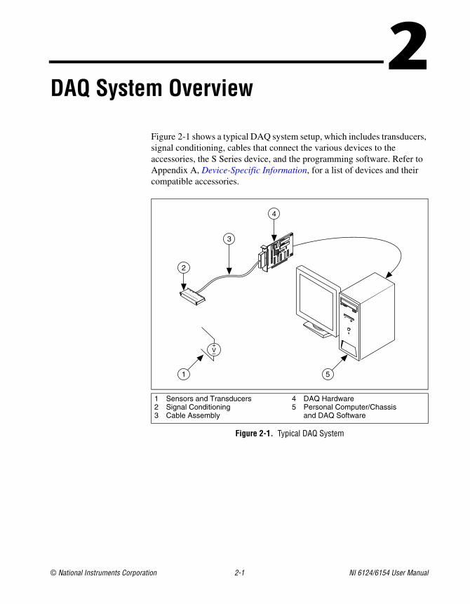
Figure 2-1 shows a typical DAQ system setup, which includes transducers, signal conditioning, cables that connect the various devices to the accessories, the S Series device, and the programming software. Refer to Appendix A, Device-Specific Information, for a list of devices and their compatible accessories.
Figure 2-1. Typical DAQ System
1 Sensors and Transducers2 Signal Conditioning3 Cable Assembly
4 DAQ Hardware5 Personal Computer/Chassis
and DAQ Software
2
4
3
5
+V–
1
Chapter 2 DAQ System Overview
NI 6124/6154 User Manual 2-2 ni.com
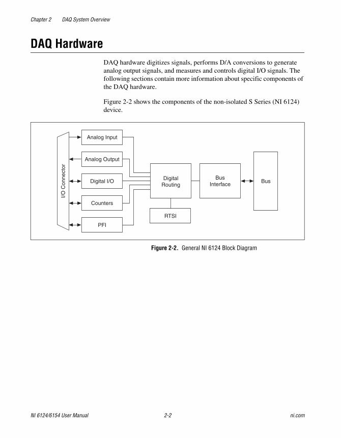
DAQ HardwareDAQ hardware digitizes signals, performs D/A conversions to generate analog output signals, and measures and controls digital I/O signals. The following sections contain more information about specific components of the DAQ hardware.
Figure 2-2 shows the components of the non-isolated S Series (NI 6124) device.
Figure 2-2. General NI 6124 Block Diagram
Analog Output
Digital I/O
Analog Input
Counters
PFI
RTSI
BusInterface Bus
I/O C
onne
ctor
DigitalRouting
Chapter 2 DAQ System Overview
© National Instruments Corporation 2-3 NI 6124/6154 User Manual
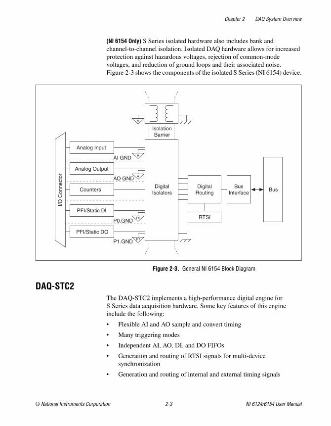
(NI 6154 Only) S Series isolated hardware also includes bank and channel-to-channel isolation. Isolated DAQ hardware allows for increased protection against hazardous voltages, rejection of common-mode voltages, and reduction of ground loops and their associated noise. Figure 2-3 shows the components of the isolated S Series (NI 6154) device.
Figure 2-3. General NI 6154 Block Diagram
DAQ-STC2The DAQ-STC2 implements a high-performance digital engine for S Series data acquisition hardware. Some key features of this engine include the following:
• Flexible AI and AO sample and convert timing
• Many triggering modes
• Independent AI, AO, DI, and DO FIFOs
• Generation and routing of RTSI signals for multi-device synchronization
• Generation and routing of internal and external timing signals
P1.GND
Analog Output
Analog Input
PFI/Static DI
PFI/Static DO
DigitalRouting
BusInterface
I/O C
onne
ctor
RTSI
DigitalIsolators
IsolationBarrier
A
Counters
P0.GND
AO GND
AI GND
P0
A
A
Bus
P1
Chapter 2 DAQ System Overview
NI 6124/6154 User Manual 2-4 ni.com
• Two flexible 32-bit counter/timer modules with hardware gating
• Digital waveform acquisition and generation
• Static DIO signals
• True 5 V high current drive DO
• PLL for clock synchronization
• PCI/PXI interface
• Independent scatter-gather DMA controllers for all acquisition and generation functions
Calibration CircuitryCalibration is the process of making adjustments to a measurement device to reduce errors associated with measurements. Without calibration, the measurement results of your device will drift over time and temperature. Calibration adjusts for these changes to improve measurement accuracy and ensure that your product meets its required specifications.
DAQ devices have high precision analog circuits that must be adjusted to obtain optimum accuracy in your measurements. Calibration determines what adjustments these analog circuits should make to the device measurements. During calibration, the value of a known, high precision measurement source is compared to the value your device acquires or generates. The adjustment values needed to minimize the difference between the known and measured values are stored in the EEPROM of the device as calibration constants. Before performing a measurement, these constants are read out of the EEPROM and are used to adjust the calibration hardware on the device. NI-DAQmx determines when this is necessary and does it automatically. If you are not using NI-DAQmx, you must load these values yourself.
You can calibrate S Series devices in two ways—through internal (or self-calibration) or through external calibration.
Internal or Self-CalibrationSelf-calibration is a process to adjust the device relative to a highly accurate and stable internal reference on the device. Self-calibration is similar to the autocalibration or autozero found on some instruments. You should perform a self-calibration whenever environmental conditions, such as ambient temperature, change significantly. To perform self-calibration, use the self-calibrate function or VI that is included with your driver software. Self-calibration requires no external connections.
Chapter 2 DAQ System Overview
© National Instruments Corporation 2-5 NI 6124/6154 User Manual
External CalibrationExternal calibration is a process to adjust the device relative to a traceable, high precision calibration standard. The accuracy specifications of your device change depending on how long it has been since your last external calibration. National Instruments recommends that you calibrate your device at least as often as the intervals listed in the accuracy specifications.
For a detailed calibration procedure for NI 6154 S Series devices, refer to the Isolated M/S Series Calibration Procedure, which you can find at ni.com/calibration and selecting Manual Calibration Procedures.
Signal ConditioningMany sensors and transducers require signal conditioning before a computer-based measurement system can effectively and accurately acquire the signal. The front-end signal conditioning system can include functions such as signal amplification, attenuation, filtering, electrical isolation, simultaneous sampling, and multiplexing. In addition, many transducers require excitation currents or voltages, bridge completion, linearization, or high amplification for proper and accurate operation. Therefore, most computer-based measurement systems include some form of signal conditioning in addition to plug-in data acquisition DAQ devices.
Sensors and TransducersSensors can generate electrical signals to measure physical phenomena, such as temperature, force, sound, or light. Some commonly used sensors are strain gages, thermocouples, thermistors, angular encoders, linear encoders, and resistance temperature detectors (RTDs).
To measure signals from these various transducers, you must convert them into a form that a DAQ device can accept. For example, the output voltage of most thermocouples is very small and susceptible to noise. Therefore, you may need to amplify or filter the thermocouple output before digitizing it. The manipulation of signals to prepare them for digitizing is called signal conditioning.
For more information about sensors, refer to the following documents.
• For general information about sensors, visit ni.com/sensors.
• If you are using LabVIEW, refer to the LabVIEW Help by selecting Help»Search the LabVIEW Help in LabVIEW and then navigate to the Taking Measurements book on the Contents tab.
Chapter 2 DAQ System Overview
NI 6124/6154 User Manual 2-6 ni.com
• If you are using other application software, refer to Common Sensors in the NI-DAQmx Help or the LabVIEW Help in version 8.0 or later.
Programming Devices in SoftwareNational Instruments measurement devices are packaged with NI-DAQmx driver software, an extensive library of functions and VIs you can call from your application software, such as LabVIEW or LabWindows/CVI, to program all the features of your NI measurement devices. NI-DAQmx driver software has an application programming interface (API), which is a library of VIs, functions, classes, attributes, and properties for creating applications for your device.
NI-DAQ includes two NI-DAQ drivers—Traditional NI-DAQ (Legacy) and NI-DAQmx. DAQ-STC2-based S Series devices use the NI-DAQmx driver. Each driver has its own API, hardware configuration, and software configuration. Refer to the DAQ Getting Started Guide for more information about the two drivers.
NI-DAQmx includes a collection of programming examples to help you get started developing an application. You can modify example code and save it in an application. You can use examples to develop a new application or add example code to an existing application.
To locate LabVIEW and LabWindows/CVI examples, open the National Instruments Example Finder. In LabVIEW and LabWindows/CVI, select Help»Find Examples.
Measurement Studio, Visual Basic, and ANSI C examples are in the following directories:
• NI-DAQmx examples for Measurement Studio-supported languages are in the following directories:
– MeasurementStudio\VCNET\Examples\NIDaq
– MeasurementStudio\DotNET\Examples\NIDaq
• NI-DAQmx examples for ANSI C are in the NI-DAQ\Examples\DAQmx ANSI C Dev directory
For additional examples, refer to zone.ni.com.
© National Instruments Corporation 3-1 NI 6124/6154 User Manual
3I/O Connector
This chapter contains information about the S Series I/O connector. Refer to one of the following sections, depending on your device:
• NI 6124 I/O Connector Signal Descriptions
• NI 6154 I/O Connector Signal Descriptions
Refer to Appendix A, Device-Specific Information, for the I/O connector pinout for your device.
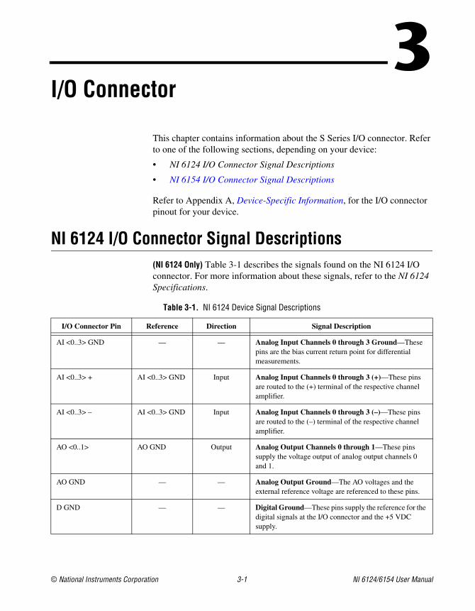
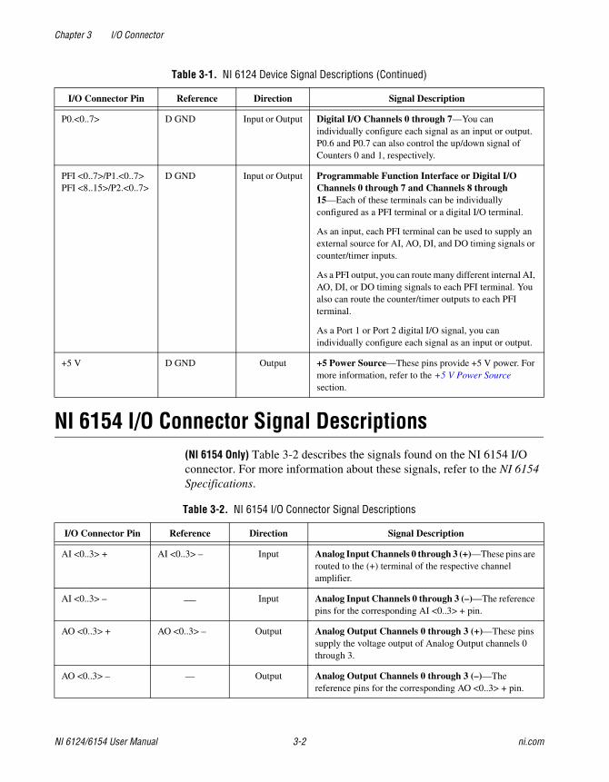
NI 6124 I/O Connector Signal Descriptions(NI 6124 Only) Table 3-1 describes the signals found on the NI 6124 I/O connector. For more information about these signals, refer to the NI 6124 Specifications.
Table 3-1. NI 6124 Device Signal Descriptions
I/O Connector Pin Reference Direction Signal Description
AI <0..3> GND — — Analog Input Channels 0 through 3 Ground—These pins are the bias current return point for differential measurements.
AI <0..3> + AI <0..3> GND Input Analog Input Channels 0 through 3 (+)—These pins are routed to the (+) terminal of the respective channel amplifier.
AI <0..3> – AI <0..3> GND Input Analog Input Channels 0 through 3 (–)—These pins are routed to the (–) terminal of the respective channel amplifier.
AO <0..1> AO GND Output Analog Output Channels 0 through 1—These pins supply the voltage output of analog output channels 0 and 1.
AO GND — — Analog Output Ground—The AO voltages and the external reference voltage are referenced to these pins.
D GND — — Digital Ground—These pins supply the reference for the digital signals at the I/O connector and the +5 VDC supply.
Chapter 3 I/O Connector
NI 6124/6154 User Manual 3-2 ni.com
NI 6154 I/O Connector Signal Descriptions(NI 6154 Only) Table 3-2 describes the signals found on the NI 6154 I/O connector. For more information about these signals, refer to the NI 6154 Specifications.
P0.<0..7> D GND Input or Output Digital I/O Channels 0 through 7—You can individually configure each signal as an input or output. P0.6 and P0.7 can also control the up/down signal of Counters 0 and 1, respectively.
PFI <0..7>/P1.<0..7> PFI <8..15>/P2.<0..7>
D GND Input or Output Programmable Function Interface or Digital I/O Channels 0 through 7 and Channels 8 through 15—Each of these terminals can be individually configured as a PFI terminal or a digital I/O terminal.
As an input, each PFI terminal can be used to supply an external source for AI, AO, DI, and DO timing signals or counter/timer inputs.
As a PFI output, you can route many different internal AI, AO, DI, or DO timing signals to each PFI terminal. You also can route the counter/timer outputs to each PFI terminal.
As a Port 1 or Port 2 digital I/O signal, you can individually configure each signal as an input or output.
+5 V D GND Output +5 Power Source—These pins provide +5 V power. For more information, refer to the +5 V Power Source section.
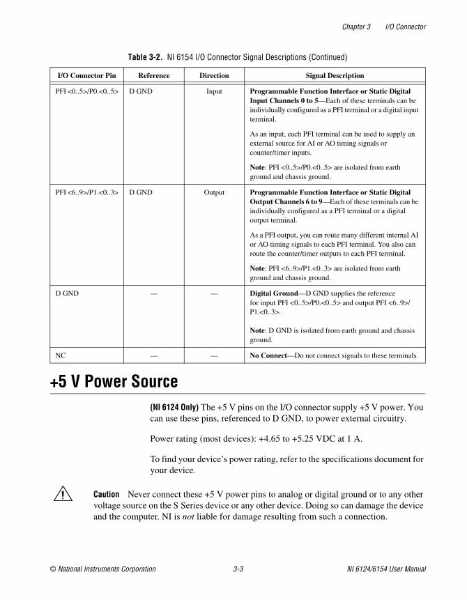
Table 3-2. NI 6154 I/O Connector Signal Descriptions
I/O Connector Pin Reference Direction Signal Description
AI <0..3> + AI <0..3> – Input Analog Input Channels 0 through 3 (+)—These pins are routed to the (+) terminal of the respective channel amplifier.
AI <0..3> – — Input Analog Input Channels 0 through 3 (–)—The reference pins for the corresponding AI <0..3> + pin.
AO <0..3> + AO <0..3> – Output Analog Output Channels 0 through 3 (+)—These pins supply the voltage output of Analog Output channels 0 through 3.
AO <0..3> – — Output Analog Output Channels 0 through 3 (–)—The reference pins for the corresponding AO <0..3> + pin.
Table 3-1. NI 6124 Device Signal Descriptions (Continued)
I/O Connector Pin Reference Direction Signal Description
Chapter 3 I/O Connector
© National Instruments Corporation 3-3 NI 6124/6154 User Manual
+5 V Power Source(NI 6124 Only) The +5 V pins on the I/O connector supply +5 V power. You can use these pins, referenced to D GND, to power external circuitry.
Power rating (most devices): +4.65 to +5.25 VDC at 1 A.
To find your device’s power rating, refer to the specifications document for your device.
Caution Never connect these +5 V power pins to analog or digital ground or to any other voltage source on the S Series device or any other device. Doing so can damage the device and the computer. NI is not liable for damage resulting from such a connection.
PFI <0..5>/P0.<0..5> D GND Input Programmable Function Interface or Static Digital Input Channels 0 to 5—Each of these terminals can be individually configured as a PFI terminal or a digital input terminal.
As an input, each PFI terminal can be used to supply an external source for AI or AO timing signals or counter/timer inputs.
Note: PFI <0..5>/P0.<0..5> are isolated from earth ground and chassis ground.
PFI <6..9>/P1.<0..3> D GND Output Programmable Function Interface or Static Digital Output Channels 6 to 9—Each of these terminals can be individually configured as a PFI terminal or a digital output terminal.
As a PFI output, you can route many different internal AI or AO timing signals to each PFI terminal. You also can route the counter/timer outputs to each PFI terminal.
Note: PFI <6..9>/P1.<0..3> are isolated from earth ground and chassis ground.
D GND — — Digital Ground—D GND supplies the reference for input PFI <0..5>/P0.<0..5> and output PFI <6..9>/P1.<0..3>.
Note: D GND is isolated from earth ground and chassis ground.
NC — — No Connect—Do not connect signals to these terminals.
Table 3-2. NI 6154 I/O Connector Signal Descriptions (Continued)
I/O Connector Pin Reference Direction Signal Description
© National Instruments Corporation 4-1 NI 6124/6154 User Manual
4Analog Input
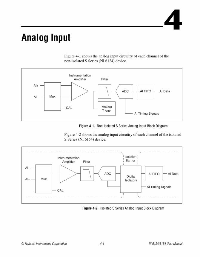
Figure 4-1 shows the analog input circuitry of each channel of the non-isolated S Series (NI 6124) device.
Figure 4-1. Non-Isolated S Series Analog Input Block Diagram
Figure 4-2 shows the analog input circuitry of each channel of the isolated S Series (NI 6154) device.
Figure 4-2. Isolated S Series Analog Input Block Diagram
InstrumentationAmplifier
AnalogTrigger
AI FIFOADC
CAL
Mux
AI+
AI–
Filter
AI Data
AI Timing Signals
InstrumentationAmplifier
AI FIFOADC
CAL
Mux
AI+
AI–
Filter
AI Data
AI Timing Signals
IsolationBarrier
DigitalIsolators
Chapter 4 Analog Input
NI 6124/6154 User Manual 4-2 ni.com
On S Series devices, each channel uses its own instrumentation amplifier, FIFO, multiplexer (mux), and A/D converter (ADC) to achieve simultaneous data acquisition. The main blocks featured in the S Series analog input circuitry are as follows:
• Mux—By default, the mux is set to route AI signals to the analog front end. When you calibrate your device, the state of the mux switches. You can manually switch the state of the mux to measure AI GND.
• Instrumentation Amplifier—The instrumentation amplifier can amplify or attenuate an AI signal to ensure that you get the maximum resolution of the ADC. Some S Series devices provide programmable instrumentation amplifiers that allow you to select the input range.
• Analog Trigger—(NI 6124 Only) For information about the trigger circuitry of S Series devices, refer to the Analog Input Triggering section.
• Filter—The filter on these S Series devices minimizes high frequency noise and some attenuating signals by 3 dB at 2 MHz.
• ADC—The analog-to-digital converter (ADC) digitizes the AI signal by converting the analog voltage into a digital number.
• AI Timing Signals—For information about the analog input timing signals available on S Series devices, refer to the Analog Input Timing Signals section.
• Isolation Barrier and Digital Isolators—(NI 6154 Only) The digital isolators across the isolation barrier provide a ground break between the isolated analog front end and the chassis ground. For more information about isolation and digital isolators, refer to the NI 6154 Isolation and Digital Isolators section of Appendix A, Device-Specific Information.
• AI FIFO—A large first-in-first-out (FIFO) buffer, located inside the FPGA, holds data during A/D conversions to ensure that no data is lost. S Series devices can handle multiple A/D conversion operations with DMA, interrupts, or programmed I/O.
Analog Input Terminal ConfigurationS Series devices support only differential (DIFF) input mode. The channels on S Series devices are true differential inputs, meaning both positive and negative inputs can carry signals of interest. For more information about DIFF input, refer to the Connecting Analog Input Signals section, which contains diagrams showing the signal paths for DIFF input mode.
Chapter 4 Analog Input
© National Instruments Corporation 4-3 NI 6124/6154 User Manual
Caution Exceeding the differential and common-mode input ranges distorts the input signals. Exceeding the maximum input voltage rating can damage the device and the computer. NI is not liable for any damage resulting from such signal connections. The maximum input voltage ratings can be found in the specifications document for each S Series device.
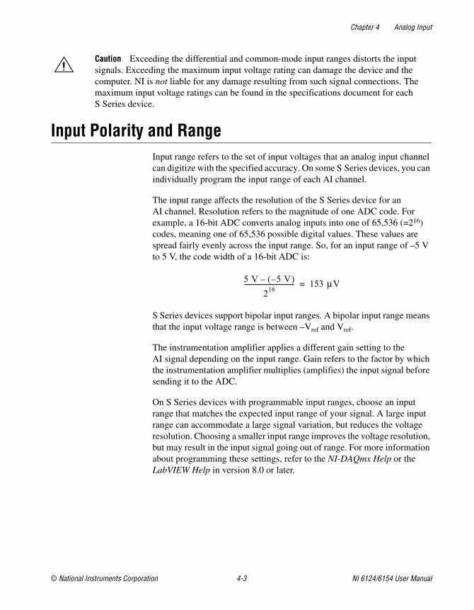
Input Polarity and RangeInput range refers to the set of input voltages that an analog input channel can digitize with the specified accuracy. On some S Series devices, you can individually program the input range of each AI channel.
The input range affects the resolution of the S Series device for an AI channel. Resolution refers to the magnitude of one ADC code. For example, a 16-bit ADC converts analog inputs into one of 65,536 (=216) codes, meaning one of 65,536 possible digital values. These values are spread fairly evenly across the input range. So, for an input range of –5 V to 5 V, the code width of a 16-bit ADC is:
S Series devices support bipolar input ranges. A bipolar input range means that the input voltage range is between –Vref and Vref.
The instrumentation amplifier applies a different gain setting to the AI signal depending on the input range. Gain refers to the factor by which the instrumentation amplifier multiplies (amplifies) the input signal before sending it to the ADC.
On S Series devices with programmable input ranges, choose an input range that matches the expected input range of your signal. A large input range can accommodate a large signal variation, but reduces the voltage resolution. Choosing a smaller input range improves the voltage resolution, but may result in the input signal going out of range. For more information about programming these settings, refer to the NI-DAQmx Help or the LabVIEW Help in version 8.0 or later.
5 V 5 V–( )–
216-------------------------------- 153 μV=
Chapter 4 Analog Input
NI 6124/6154 User Manual 4-4 ni.com
Working Voltage RangeOn most S Series devices, the PGIA operates normally by amplifying signals of interest while rejecting common-mode signals under the following three conditions:
• The common-mode voltage (Vcm), which is equivalent to subtracting AI <0..x> GND from AI <0..x> –, must be less than ±10 V. This Vcm is a constant for all range selections.
• The signal voltage (Vs), which is equivalent to subtracting AI <0..x> + from AI <0..x> –, must be less than or equal to the range selection of the given channel. If Vs is greater than the range selected, the signal clips and information are lost.
• The total working voltage of the positive input, which is equivalent to (Vcm + Vs), or subtracting AI <0..x> GND from AI <0..x> +, must be less than ±11 V.
If any of these conditions are exceeded, the input voltage is clamped until the fault condition is removed.
Note All inputs are protected at up to ±35 V.
(NI 6154 Only) The isolation features of the NI 6154 improve the working voltage range in your applications. Refer to the NI 6154 Specifications for more information.
AI Data Acquisition MethodsWhen performing analog input measurements, there are several different data acquisition methods available. You can either perform software-timed or hardware-timed acquisitions:
• Software-Timed Acquisitions—With a software-timed acquisition, software controls the rate of the acquisition. Software sends a separate command to the hardware to initiate each ADC conversion. In NI-DAQmx, software-timed acquisitions are referred to as having On Demand timing. Software-timed acquisitions are also referred to as immediate or static acquisitions and are typically used for reading a single point of data.
• Hardware-Timed Acquisitions—With hardware-timed acquisitions, a digital hardware signal controls the rate of the acquisition. This signal can be generated internally on your device or provided externally.
Chapter 4 Analog Input
© National Instruments Corporation 4-5 NI 6124/6154 User Manual
Hardware-timed acquisitions have several advantages over software-timed acquisitions:
– The time between samples can be much shorter.
– The timing between samples can be deterministic.
– Hardware-timed acquisitions can use hardware triggering. For more information, refer to Chapter 11, Triggering.
Hardware-timed operations can be buffered or non-buffered. A buffer is a temporary storage in the computer memory where acquired samples are stored.
– Buffered—In a buffered acquisition, data is moved from the DAQ device’s onboard FIFO memory to a PC buffer using DMA or interrupts before it is transferred to ADE memory. Buffered acquisitions typically allow for much faster transfer rates than non-buffered acquisitions because data is moved in large blocks, rather than one point at a time. For more information about DMA and interrupts, refer to the Data Transfer Methods section of Chapter 10, Bus Interface.
One property of buffered I/O operations is the sample mode. The sample mode can be either finite or continuous.
Finite sample mode acquisition refers to the acquisitions of a specific, predetermined number of data samples. After the specified number of samples has been collected into the buffer, the acquisition stops. If you use a reference trigger, you must use finite sample mode. Refer to the AI Reference Trigger Signal section for more information.
Continuous acquisition refers to the acquisition of an unspecified number of samples. Instead of acquiring a set number of data samples and stopping, a continuous acquisition continues until you stop the operation. A continuous acquisition is also referred to as double-buffered or circular-buffered acquisition.
If data cannot be transferred across the bus fast enough, the data in the FIFO will be overwritten and an error will be generated. With continuous operations, if the user program does not read data out of the PC buffer fast enough to keep up with the data transfer, the buffer could reach an overflow condition, causing an error to be generated.
– Non-Buffered—In non-buffered acquisitions, data is read directly from the FIFO on the device. Typically, hardware-timed non-buffered operations are used to read single samples with known time increments between them and small latency.
Chapter 4 Analog Input
NI 6124/6154 User Manual 4-6 ni.com
Analog Input TriggeringAnalog input supports two different triggering actions: start and reference. An analog or digital hardware trigger can initiate these actions. All S Series devices support digital triggering, and some also support analog triggering. To find your device’s triggering options, refer to the specifications document for your device.
The AI Start Trigger Signal and AI Reference Trigger Signal sections contain information about the analog input trigger signals.
Refer to Chapter 11, Triggering, for more information about triggers.
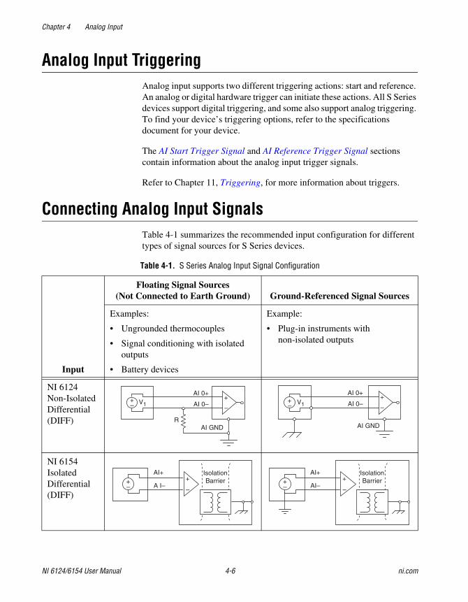
Connecting Analog Input SignalsTable 4-1 summarizes the recommended input configuration for different types of signal sources for S Series devices.
Table 4-1. S Series Analog Input Signal Configuration
Input
Floating Signal Sources (Not Connected to Earth Ground) Ground-Referenced Signal Sources
Examples:
• Ungrounded thermocouples
• Signal conditioning with isolated outputs
• Battery devices
Example:
• Plug-in instruments with non-isolated outputs
NI 6124 Non-Isolated Differential (DIFF)
NI 6154 Isolated Differential (DIFF)
AI 0+
AI 0–
AI GND
V1+–
+
–
R
V1
AI 0+
AI 0–
AI GND
+–
+
–
AI+
A I–
IsolationBarrier+
–+
–
AI+
AI–
IsolationBarrier+
–+
–
Chapter 4 Analog Input
© National Instruments Corporation 4-7 NI 6124/6154 User Manual
Refer to the Analog Input Terminal Configuration section for descriptions of the input modes.
Types of Signal SourcesWhen configuring the input channels and making signal connections, first determine whether the signal sources are floating or ground-referenced:
• Floating Signal Sources—A floating signal source is not connected in any way to the building ground system, and instead has an isolated ground-reference point. Some examples of floating signal sources are outputs of transformers, thermocouples, battery-powered devices, optical isolators, and isolation amplifiers. An instrument or device that has an isolated output is a floating signal source. You must connect the ground reference of a floating signal to the AI ground of the device to establish a local or onboard reference for the signal. Otherwise, the measured input signal varies as the source floats outside the common-mode input range.
• Ground-Referenced Signal Sources—A ground-referenced signal source is connected in some way to the building system ground and is, therefore, already connected to a common ground point with respect to the device, assuming that the computer is plugged into the same power system as the source. Non-isolated outputs of instruments and devices that plug into the building power system fall into this category.
The difference in ground potential between two instruments connected to the same building power system is typically between 1 mV and 100 mV, but the difference can be much higher if power distribution circuits are improperly connected. If a grounded signal source is incorrectly measured, this difference can appear as measurement error. Follow the connection instructions for grounded signal sources to eliminate this ground potential difference from the measured signal.
Isolated devices have isolated front ends that are isolated from ground-reference signal sources and are not connected to building system grounds. Isolated devices require the user to provide a ground-reference terminal to which its input signals are referenced.
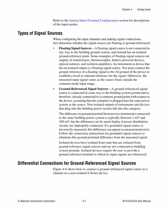
Differential Connections for Ground-Referenced Signal SourcesFigure 4-6 shows how to connect a ground-referenced signal source to a channel on a non-isolated S Series device.
Chapter 4 Analog Input
NI 6124/6154 User Manual 4-8 ni.com
Figure 4-3. Differential Connection for Ground-Referenced Signals on Non-Isolated Devices
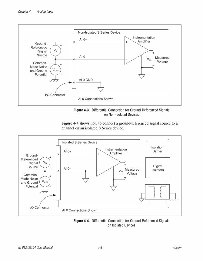
Figure 4-4 shows how to connect a ground-referenced signal source to a channel on an isolated S Series device.
Figure 4-4. Differential Connection for Ground-Referenced Signals on Isolated Devices
Ground-Referenced
SignalSource
Common-Mode Noiseand Ground
Potential
Vs
Vcm
+
–
+
–
I/O ConnectorAI 0 Connections Shown
AI 0 GND
AI 0–
AI 0++
–
+
–
VmMeasured
Voltage
InstrumentationAmplifier
Non-Isolated S Series Device
Ground-Referenced
SignalSource
Common-Mode Noiseand Ground
Potential
Vs
Vcm
+
–
+
–
I/O ConnectorAI 0 Connections Shown
AI 0–
AI 0++
–
+
–
VmMeasured
Voltage
InstrumentationAmplifier
Isolated S Series Device
DigitalIsolators
IsolationBarrier
Chapter 4 Analog Input
© National Instruments Corporation 4-9 NI 6124/6154 User Manual
With these types of connections, the instrumentation amplifier rejects both the common-mode noise in the signal and the ground potential difference between the signal source and the device ground, shown as Vcm in these figures.
Common-Mode Signal Rejection ConsiderationsThe instrumentation amplifier can reject any voltage caused by ground potential differences between the signal source and the device. In addition, the instrumentation amplifier can reject common-mode noise pickup in the leads connecting the signal sources to the device. The instrumentation amplifier can reject common-mode signals as long as V+in and V–in (input signals) are both within the working voltage range of the device.
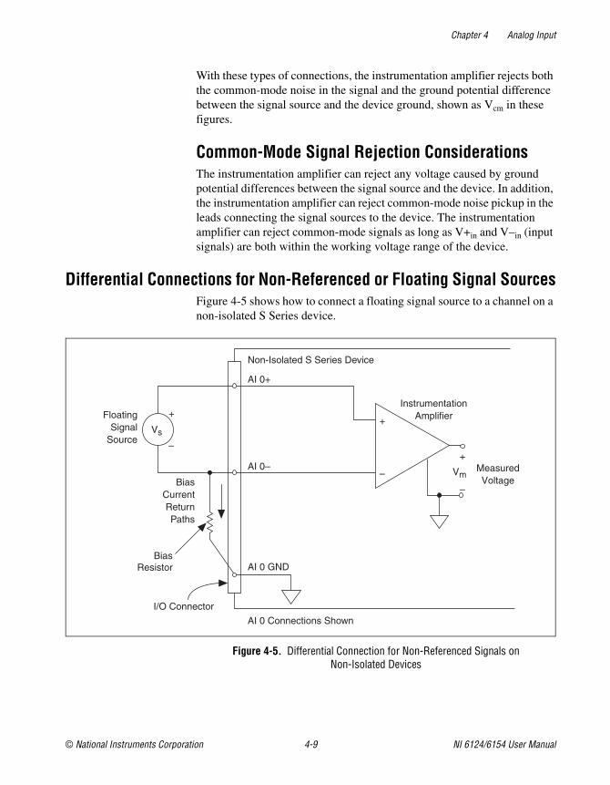
Differential Connections for Non-Referenced or Floating Signal SourcesFigure 4-5 shows how to connect a floating signal source to a channel on a non-isolated S Series device.
Figure 4-5. Differential Connection for Non-Referenced Signals on Non-Isolated Devices
+
+
FloatingSignal
Source
InstrumentationAmplifier
VmMeasuredVoltage
I/O Connector
AI 0 GND
BiasCurrentReturnPaths
AI 0–
AI 0+
AI 0 Connections Shown
BiasResistor
Vs
–
+
–
–
Non-Isolated S Series Device
Chapter 4 Analog Input
NI 6124/6154 User Manual 4-10 ni.com
Figure 4-5 shows a bias resistor connected between AI 0 – and the floating signal source ground. This resistor provides a return path for the bias current. A value of 10 kΩ to 100 kΩ is usually sufficient. If you do not use the resistor and the source is truly floating, the source is not likely to remain within the common-mode signal range of the instrumentation amplifier, so the instrumentation amplifier saturates, causing erroneous readings. You must reference the source to the respective channel ground.
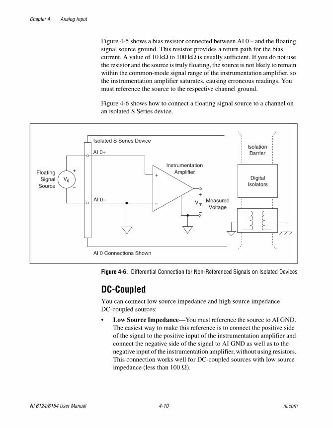
Figure 4-6 shows how to connect a floating signal source to a channel on an isolated S Series device.
Figure 4-6. Differential Connection for Non-Referenced Signals on Isolated Devices
DC-CoupledYou can connect low source impedance and high source impedance DC-coupled sources:
• Low Source Impedance—You must reference the source to AI GND. The easiest way to make this reference is to connect the positive side of the signal to the positive input of the instrumentation amplifier and connect the negative side of the signal to AI GND as well as to the negative input of the instrumentation amplifier, without using resistors. This connection works well for DC-coupled sources with low source impedance (less than 100 Ω).
+
+
FloatingSignal
Source
InstrumentationAmplifier
VmMeasuredVoltage
AI 0–
AI 0+
AI 0 Connections Shown
Vs–
+
–
–
Isolated S Series Device
DigitalIsolators
IsolationBarrier
Chapter 4 Analog Input
© National Instruments Corporation 4-11 NI 6124/6154 User Manual
• High Source Impedance—For larger source impedances, this connection leaves the DIFF signal path significantly off balance. Noise that couples electrostatically onto the positive line does not couple onto the negative line because it is connected to ground. Hence, this noise appears as a DIFF-mode signal instead of a common-mode signal, and the instrumentation amplifier does not reject it. In this case, instead of directly connecting the negative line to AI GND, connect the negative line to AI GND through a resistor that is about 100 times the equivalent source impedance. The resistor puts the signal path nearly in balance, so that about the same amount of noise couples onto both connections, yielding better rejection of electrostatically coupled noise. This configuration does not load down the source (other than the very high input impedance of the instrumentation amplifier).
You can fully balance the signal path by connecting another resistor of the same value between the positive input and AI GND. This fully balanced configuration offers slightly better noise rejection but has the disadvantage of loading the source down with the series combination (sum) of the two resistors. If, for example, the source impedance is 2 kΩ and each of the two resistors is 100 kΩ, the resistors load down the source with 200 kΩ and produce a –1% gain error.
AC-CoupledBoth inputs of the instrumentation amplifier require a DC path to ground in order for the instrumentation amplifier to work. If the source is AC-coupled (capacitively coupled), the instrumentation amplifier needs a resistor between the positive input and AI GND. If the source has low-impedance, choose a resistor that is large enough not to significantly load the source but small enough not to produce significant input offset voltage as a result of input bias current (typically 100 kΩ to 1 MΩ). In this case, connect the negative input directly to AI GND. If the source has high output impedance, balance the signal path as previously described using the same value resistor on both the positive and negative inputs; be aware that there is some gain error from loading down the source.
Field Wiring ConsiderationsEnvironmental noise can seriously affect the measurement accuracy of the S Series device if you do not take proper care when running signal wires between signal sources and the device. The following recommendations apply mainly to AI signal routing, although they also apply to signal routing in general.
Chapter 4 Analog Input
NI 6124/6154 User Manual 4-12 ni.com
Minimize noise pickup and maximize measurement accuracy by taking the following precautions.
• Use differential AI connections to reject common-mode noise.
• Use individually shielded, twisted-pair wires to connect AI signals to the device. With this type of wire, the signals attached to the AI + and AI – inputs are twisted together and then covered with a shield. You then connect this shield only at one point to the signal source ground. This kind of connection is required for signals traveling through areas with large magnetic fields or high electromagnetic interference.
• Route signals to the device carefully. Keep cabling away from noise sources. The most common noise source in a PCI DAQ system is the video monitor. Separate the monitor from the analog signals as far as possible.
• Separate the signal lines of the S Series device from high-current or high-voltage lines. These lines can induce currents in or voltages on the signal lines of the S Series device if they run in close parallel paths. To reduce the magnetic coupling between lines, separate them by a reasonable distance if they run in parallel, or run the lines at right angles to each other.
• Do not run signal lines through conduits that also contain power lines.
• Protect signal lines from magnetic fields caused by electric motors, welding equipment, breakers, or transformers by running them through special metal conduits.
Refer to the NI Developer Zone document, Field Wiring and Noise Considerations for Analog Signals, for more information.
Minimizing Drift in Differential ModeIf the readings from the DAQ device are random and drift rapidly, you should check the ground-reference connections. The signal can be referenced to a level that is considered floating with reference to the device ground reference. Even though you are in DIFF mode, you must still reference the signal to the same ground level as the device reference. There are various methods of achieving this reference while maintaining a high common-mode rejection ratio (CMRR). These methods are outlined in the Connecting Analog Input Signals section.
AI GND is an AI common signal that routes directly to the ground connection point on the devices. You can use this signal if you need a general analog ground connection point to the device.
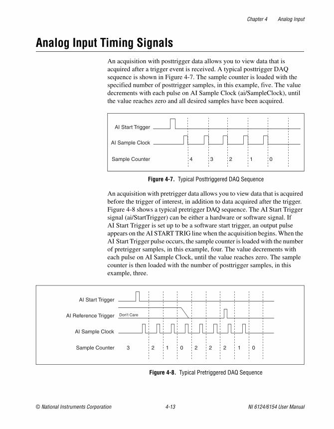
Chapter 4 Analog Input
© National Instruments Corporation 4-13 NI 6124/6154 User Manual
Analog Input Timing SignalsAn acquisition with posttrigger data allows you to view data that is acquired after a trigger event is received. A typical posttrigger DAQ sequence is shown in Figure 4-7. The sample counter is loaded with the specified number of posttrigger samples, in this example, five. The value decrements with each pulse on AI Sample Clock (ai/SampleClock), until the value reaches zero and all desired samples have been acquired.
Figure 4-7. Typical Posttriggered DAQ Sequence
An acquisition with pretrigger data allows you to view data that is acquired before the trigger of interest, in addition to data acquired after the trigger. Figure 4-8 shows a typical pretrigger DAQ sequence. The AI Start Trigger signal (ai/StartTrigger) can be either a hardware or software signal. If AI Start Trigger is set up to be a software start trigger, an output pulse appears on the AI START TRIG line when the acquisition begins. When the AI Start Trigger pulse occurs, the sample counter is loaded with the number of pretrigger samples, in this example, four. The value decrements with each pulse on AI Sample Clock, until the value reaches zero. The sample counter is then loaded with the number of posttrigger samples, in this example, three.
Figure 4-8. Typical Pretriggered DAQ Sequence
13 04 2
AI Start Trigger
AI Sample Clock
Sample Counter
Don't Care
0 123 1 02 2 2
AI Start Trigger
AI Reference Trigger
AI Sample Clock
Sample Counter
Chapter 4 Analog Input
NI 6124/6154 User Manual 4-14 ni.com
If an AI Reference Trigger (ai/ReferenceTrigger) pulse occurs before the specified number of pretrigger samples are acquired, the trigger pulse is ignored. Otherwise, when the AI Reference Trigger pulse occurs, the sample counter value decrements until the specified number of posttrigger samples have been acquired. For more information about start and reference triggers, refer to the Analog Input Triggering section.
In order to provide all of the timing functionality described throughout this section, the DAQ-STC2 provides an extremely powerful and flexible timing engine. For more information about all of the clock routing and timing options that the analog input timing engine provides, refer to the NI-DAQmx Help or the LabVIEW Help in version 8.0 or later.
S Series devices feature the following analog input timing signals:
• AI Sample Clock Signal
• AI Sample Clock Timebase Signal
• AI Convert Clock Signal
• AI Convert Clock Timebase Signal
• AI Hold Complete Event Signal
• AI Start Trigger Signal
• AI Reference Trigger Signal
AI Sample Clock SignalUse the AI Sample Clock (ai/SampleClock) signal to initiate a set of measurements. Your S Series device samples the AI signals of every channel in the task once for every AI Sample Clock.
You can specify an internal or external source for AI Sample Clock. You also can specify whether the measurement sample begins on the rising edge or falling edge of AI Sample Clock.
Using an Internal SourceOne of the following internal signals can drive AI Sample Clock:
• Counter n Internal Output
• AI Sample Clock Timebase (divided down)
• A pulse initiated by host software
A programmable internal counter divides down the sample clock timebase.
Chapter 4 Analog Input
© National Instruments Corporation 4-15 NI 6124/6154 User Manual
Several other internal signals can be routed to AI Sample Clock through RTSI. Refer to Device Routing in MAX in the NI-DAQmx Help or the LabVIEW Help in version 8.0 or later for more information.
Using an External SourceUse one of the following external signals as the source of AI Sample Clock:
• PFI <0..15>
• RTSI <0..7>
• PXI_STAR
• Analog Comparison Event (an analog trigger)
Routing AI Sample Clock Signal to an Output TerminalYou can route AI Sample Clock out to any PFI <0..15> or RTSI <0..7> terminal. This pulse is always active high.
You can specify the output to have one of two behaviors. With the pulse behavior, your DAQ device briefly pulses the PFI terminal once for every occurrence of AI Sample Clock.
With level behavior, your DAQ device drives the PFI terminal high during the entire sample.
All PFI terminals are configured as inputs by default.
Other Timing RequirementsA counter on your device internally generates AI Sample Clock unless you select some external source. AI Start Trigger starts this counter and either software or hardware can stop it once a finite acquisition completes. When using an internally generated AI Sample Clock, you also can specify a configurable delay from AI Start Trigger to the first AI Sample Clock pulse. By default, this delay is set to two ticks of the AI Sample Clock Timebase signal.
Chapter 4 Analog Input
NI 6124/6154 User Manual 4-16 ni.com
Figure 4-9 shows the relationship of AI Sample Clock to AI Start Trigger.
Figure 4-9. AI Sample Clock and AI Start Trigger
AI Sample Clock Timebase SignalYou can route any of the following signals to be the AI Sample Clock Timebase (ai/SampleClockTimebase) signal:
• 20 MHz Timebase
• 100 kHz Timebase
• PXI_CLK10
• RTSI <0..7>
• PFI <0..15>
• PXI_STAR
• Analog Comparison Event (an analog trigger)
AI Sample Clock Timebase is not available as an output on the I/O connector. AI Sample Clock Timebase is divided down to provide one of the possible sources for AI Sample Clock. You can configure the polarity selection for AI Sample Clock Timebase as either rising or falling edge.
AI Convert Clock SignalUse the AI Convert Clock (ai/ConvertClock) signal to initiate a single A/D conversion on every channel.
You can specify either an internal or external signal as the source of AI Convert Clock. You also can specify whether the measurement sample begins on the rising edge or falling edge of AI Convert Clock.
AI Sample Clock Timebase
AI Start Trigger
AI Sample Clock
Delay From Start
Trigger
Chapter 4 Analog Input
© National Instruments Corporation 4-17 NI 6124/6154 User Manual
Using an Internal SourceOne of the following internal signals can drive AI Convert Clock:
• AI Convert Clock Timebase (divided down)
• Counter n Internal Output
A programmable internal counter divides down the AI Convert Clock Timebase to generate AI Convert Clock. The counter is started by AI Sample Clock and continues to count down to zero, produces an AI Convert Clock, reloads itself, and repeats the process until the sample is finished. It then reloads itself in preparation for the next AI Sample Clock pulse.
Using an External SourceUse one of the following external signals as the source of AI Convert Clock:
• PFI <0..15>
• RTSI <0..7>
• PXI_STAR
• Analog Comparison Event (an analog trigger)
Routing AI Convert Clock Signal to an Output TerminalYou can route AI Convert Clock (as an active low signal) out to any PFI <0..15> or RTSI <0..7> terminal.
All PFI terminals are configured as inputs by default.
AI Convert Clock Timebase SignalThe AI Convert Clock Timebase (ai/ConvertClockTimebase) signal is divided down to provide on of the possible sources for AI Convert Clock. Use one of the following signals as the source of AI Convert Clock Timebase:
• AI Sample Clock Timebase
• 20 MHz Timebase
AI Convert Clock Timebase is not available as an output on the I/O connector.
Chapter 4 Analog Input
NI 6124/6154 User Manual 4-18 ni.com
AI Hold Complete Event SignalThe AI Hold Complete Event (ai/HoldCompleteEvent) signal generates a pulse after each A/D conversion begins. You can route ai/HoldCompleteEvent out to any PFI <0..15> or RTSI <0..7> terminal.
The polarity of ai/HoldCompleteEvent is software-selectable, but is typically configured so that a low-to-high leading edge can clock external AI multiplexers indicating when the input signal has been sampled and can be removed.
AI Start Trigger SignalUse the AI Start Trigger (ai/StartTrigger) signal to begin a measurement acquisition. A measurement acquisition consists of one or more samples. If you do not use triggers, begin a measurement with a software command. Once the acquisition begins, configure the acquisition to stop:
• When a certain number of points are sampled (in finite mode)
• After a hardware reference trigger (in finite mode)
• With a software command (in continuous mode)
An acquisition that uses a start trigger (but not a reference trigger) is sometimes referred to as a posttriggered acquisition.
Using a Digital SourceTo use AI Start Trigger with a digital source, specify a source and an edge. The source can be any of the following signals:
• PFI <0..15>
• RTSI <0..7>
• Counter n Internal Output
• PXI_STAR
The source also can be one of several other internal signals on your DAQ device. Refer to Device Routing in MAX in the NI-DAQmx Help or the LabVIEW Help in version 8.0 or later for more information.
You also can specify whether the measurement acquisition begins on the rising edge or falling edge of AI Start Trigger.
Chapter 4 Analog Input
© National Instruments Corporation 4-19 NI 6124/6154 User Manual
Using an Analog SourceWhen you use an analog trigger source, the acquisition begins on the first rising edge of the Analog Comparison Event signal.
Routing AI Start Trigger to an Output TerminalYou can route AI Start Trigger out to any PFI <0..15> or RTSI <0..7> terminal. The output is an active high pulse. All PFI terminals are configured as inputs by default.
The device also uses AI Start Trigger to initiate pretriggered DAQ operations. In most pretriggered applications, a software trigger generates AI Start Trigger. Refer to the AI Reference Trigger Signal section for a complete description of the use of AI Start Trigger and AI Reference Trigger in a pretriggered DAQ operation.
AI Reference Trigger SignalUse AI Reference Trigger (ai/ReferenceTrigger) signal to stop a measurement acquisition. To use a reference trigger, specify a buffer of finite size and a number of pretrigger samples (samples that occur before the reference trigger). The number of posttrigger samples (samples that occur after the reference trigger) desired is the buffer size minus the number of pretrigger samples.
Once the acquisition begins, the DAQ device writes samples to the buffer. After the DAQ device captures the specified number of pretrigger samples, the DAQ device begins to look for the reference trigger condition. If the reference trigger condition occurs before the DAQ device captures the specified number of pretrigger samples, the DAQ device ignores the condition.
If the buffer becomes full, the DAQ device continuously discards the oldest samples in the buffer to make space for the next sample. This data can be accessed (with some limitations) before the DAQ device discards it. Refer to the KnowledgeBase document, Can a Pretriggered Acquisition be Continuous?, for more information. To access this KnowledgeBase, go to ni.com/info and enter the info code rdcanq.
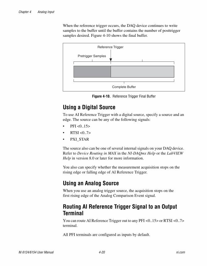
Chapter 4 Analog Input
NI 6124/6154 User Manual 4-20 ni.com
When the reference trigger occurs, the DAQ device continues to write samples to the buffer until the buffer contains the number of posttrigger samples desired. Figure 4-10 shows the final buffer.
Figure 4-10. Reference Trigger Final Buffer
Using a Digital SourceTo use AI Reference Trigger with a digital source, specify a source and an edge. The source can be any of the following signals:
• PFI <0..15>
• RTSI <0..7>
• PXI_STAR
The source also can be one of several internal signals on your DAQ device. Refer to Device Routing in MAX in the NI-DAQmx Help or the LabVIEW Help in version 8.0 or later for more information.
You also can specify whether the measurement acquisition stops on the rising edge or falling edge of AI Reference Trigger.
Using an Analog SourceWhen you use an analog trigger source, the acquisition stops on the first rising edge of the Analog Comparison Event signal.
Routing AI Reference Trigger Signal to an Output TerminalYou can route AI Reference Trigger out to any PFI <0..15> or RTSI <0..7> terminal.
All PFI terminals are configured as inputs by default.
Reference Trigger
Pretrigger Samples
Complete Buffer
Chapter 4 Analog Input
© National Instruments Corporation 4-21 NI 6124/6154 User Manual
Getting Started with AI Applications in SoftwareYou can use the S Series device in the following analog input applications:
• Simultaneous sampling
• Single-point analog input
• Finite analog input
• Continuous analog input
You can perform these applications through DMA, interrupt, or programmed I/O data transfer mechanisms. Some of the applications also use start and reference pause triggers.
Note For more information about programming analog input applications and triggers in software, refer to the NI-DAQmx Help or the LabVIEW Help in version 8.0 or later.
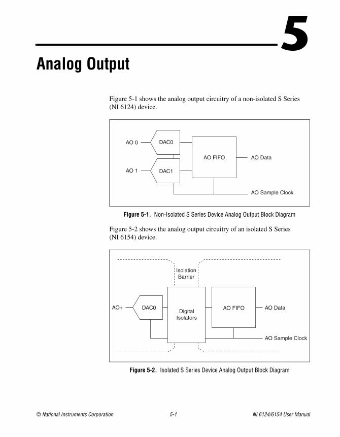
© National Instruments Corporation 5-1 NI 6124/6154 User Manual
5Analog Output
Figure 5-1 shows the analog output circuitry of a non-isolated S Series (NI 6124) device.
Figure 5-1. Non-Isolated S Series Device Analog Output Block Diagram
Figure 5-2 shows the analog output circuitry of an isolated S Series (NI 6154) device.
Figure 5-2. Isolated S Series Device Analog Output Block Diagram
AO 0
AO 1
DAC0
DAC1
AO FIFO AO Data
AO Sample Clock
AO+ DAC0 AO FIFO AO Data
AO Sample Clock
IsolationBarrier
DigitalIsolators
Chapter 5 Analog Output
NI 6124/6154 User Manual 5-2 ni.com
The main blocks featured in the S Series analog output circuitry are as follows:
• AO FIFO—The AO FIFO enables analog output waveform generation. It is a first-in-first-out (FIFO) memory buffer between the computer and the DACs that allows you to download all the points of a waveform to your board without host computer interaction.
• AO Sample Clock—The DAC reads a sample from the FIFO with every cycle of the AO Sample Clock signal and generates the AO voltage. For more information, refer to the AO Sample Clock Signal section.
• Isolation Barrier and Digital Isolators—(NI 6154 Only) The digital isolators across the isolation barrier provide a ground break between the isolated analog front end and the chassis ground. For more information about isolation and digital isolators, refer to the NI 6154 Isolation and Digital Isolators section of Appendix A, Device-Specific Information.
• DAC—Digital-to-analog converters (DACs) convert digital codes to analog voltages.
Minimizing Glitches on the Output SignalWhen you use a DAC to generate a waveform, you may observe glitches on the output signal. These glitches are normal; when a DAC switches from one voltage to another, it produces glitches due to released charges. The largest glitches occur when the most significant bit (MSB) of the DAC code switches. You can build a lowpass deglitching filter to remove some of these glitches, depending on the frequency and nature of the output signal. Visit ni.com/support for more information about minimizing glitches.
AO Data Generation MethodsWhen performing an analog output operation, there are several different data generation methods available. You can either perform software-timed or hardware-timed generations:
• Software-Timed Generations—With a software-timed generation, software controls the rate at which data is generated. Software sends a separate command to the hardware to initiate each DAC conversion. In NI-DAQmx, software-timed generations are referred to as On Demand timing. Software-timed generations are also referred to as immediate or static operations. They are typically used for writing a single value out, such as a constant DC voltage.
Chapter 5 Analog Output
© National Instruments Corporation 5-3 NI 6124/6154 User Manual
• Hardware-Timed Generations—With a hardware-timed generation, a digital hardware signal controls the rate of the generation. This signal can be generated internally on your device or provided externally.
Hardware-timed generations have several advantages over software-timed generations:
– The time between samples can be much shorter.
– The timing between samples can be deterministic.
– Hardware-timed generations can use hardware triggering. For more information, refer to Chapter 11, Triggering.
Hardware-timed operations can be buffered or non-buffered. A buffer is a temporary storage in computer memory for acquired or to-be-generated samples.
– Buffered—In a buffered generation, data is moved from a PC buffer to the DAQ device’s onboard FIFO using DMA or interrupts before it is written to the DACs one sample at a time. Buffered generations typically allow for much faster transfer rates than non-buffered generations because data is moved in large blocks, rather than one point at a time. For more information about DMA and interrupts, refer to the Data Transfer Methods section of Chapter 10, Bus Interface.
One property of buffered I/O operations is the sample mode. The sample mode can be either finite or continuous.
Finite sample mode generation refers to the generation of a specific, predetermined number of data samples. When the specified number of samples has been written out, the generation stops.
Continuous generation refers to the generation of an unspecified number of samples. Instead of generating a set number of data samples and stopping, a continuous generation continues until you stop the operation. There are several different methods of continuous generation that control what data is written. These methods are regeneration, FIFO regeneration and non-regeneration modes.
Regeneration is the repetition of the data that is already in the buffer. Standard regeneration is when data from the PC buffer is continually downloaded to the FIFO to be written out. New data can be written to the PC buffer at any time without disrupting the output.
Chapter 5 Analog Output
NI 6124/6154 User Manual 5-4 ni.com
With FIFO regeneration, the entire buffer is downloaded to the FIFO and regenerated from there. After the data is downloaded, new data cannot be written to the FIFO. To use FIFO regeneration, the entire buffer must fit within the FIFO size. The advantage of using FIFO regeneration is that it does not require communication with the main host memory after the operation is started, thereby preventing any problems that may occur due to excessive bus traffic.
With non-regeneration, old data will not be repeated. New data must be continually written to the buffer. If the program does not write new data to the buffer at a fast enough rate to keep up with the generation, the buffer will underflow and cause an error.
– Non-Buffered—In hardware-timed non-buffered generations, data is written directly to the FIFO on the device. Typically, hardware-timed non-buffered operations are used to write single samples with known time increments between them and good latency.
Analog Output TriggeringAnalog output supports two different triggering actions: start and pause. An analog or digital hardware trigger can initiate these actions. All S Series devices support digital triggering, and some also support analog triggering. To find your device’s triggering options, refer to the specifications document for your device.
The AO Start Trigger Signal and AO Pause Trigger Signal sections contain information about the analog output trigger signals.
Refer to Chapter 11, Triggering, for more information about triggers.
Connecting Analog Output SignalsThe AO signals are AO 0, AO 1, and AO GND. AO 0 is the voltage output signal for AO channel 0. AO 1 is the voltage output signal for AO channel 1. AO GND is the ground reference for the AO channels.
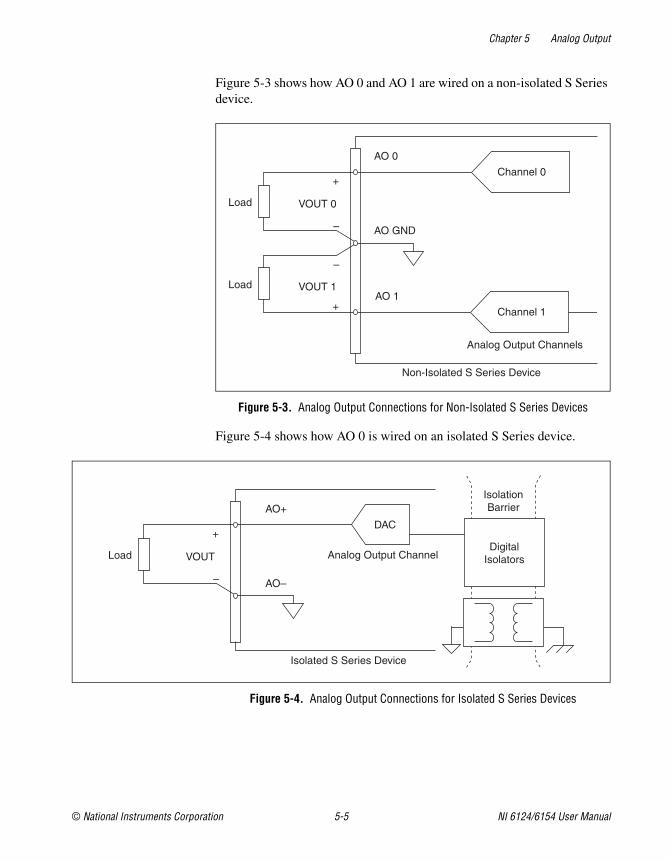
Chapter 5 Analog Output
© National Instruments Corporation 5-5 NI 6124/6154 User Manual
Figure 5-3 shows how AO 0 and AO 1 are wired on a non-isolated S Series device.
Figure 5-3. Analog Output Connections for Non-Isolated S Series Devices
Figure 5-4 shows how AO 0 is wired on an isolated S Series device.
Figure 5-4. Analog Output Connections for Isolated S Series Devices
+
–
+
–
Channel 0
Channel 1
Load
Load
VOUT 0
VOUT 1AO 1
AO GND
AO 0
Analog Output Channels
Non-Isolated S Series Device
+
–
Load VOUT
AO–
AO+
Analog Output Channel
Isolated S Series Device
DAC
DigitalIsolators
IsolationBarrier
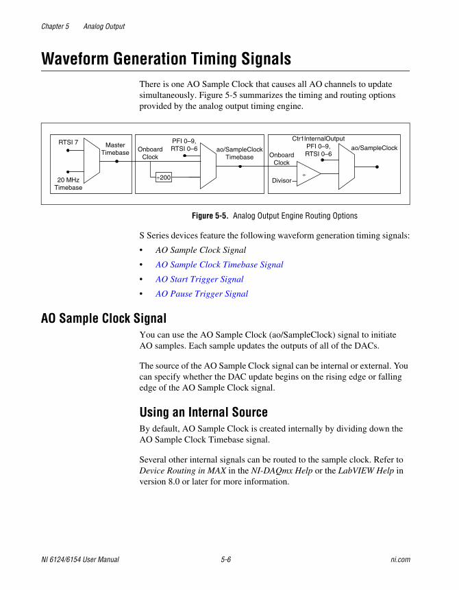
Chapter 5 Analog Output
NI 6124/6154 User Manual 5-6 ni.com
Waveform Generation Timing SignalsThere is one AO Sample Clock that causes all AO channels to update simultaneously. Figure 5-5 summarizes the timing and routing options provided by the analog output timing engine.
Figure 5-5. Analog Output Engine Routing Options
S Series devices feature the following waveform generation timing signals:
• AO Sample Clock Signal
• AO Sample Clock Timebase Signal
• AO Start Trigger Signal
• AO Pause Trigger Signal
AO Sample Clock SignalYou can use the AO Sample Clock (ao/SampleClock) signal to initiate AO samples. Each sample updates the outputs of all of the DACs.
The source of the AO Sample Clock signal can be internal or external. You can specify whether the DAC update begins on the rising edge or falling edge of the AO Sample Clock signal.
Using an Internal SourceBy default, AO Sample Clock is created internally by dividing down the AO Sample Clock Timebase signal.
Several other internal signals can be routed to the sample clock. Refer to Device Routing in MAX in the NI-DAQmx Help or the LabVIEW Help in version 8.0 or later for more information.
RTSI 7
20 MHzTimebase
÷200
MasterTimebase Onboard
Clock
PFI 0–9,RTSI 0–6 ao/SampleClock
Timebase OnboardClock
Divisor
ao/SampleClock
Ctr1InternalOutputPFI 0–9,RTSI 0–6
÷
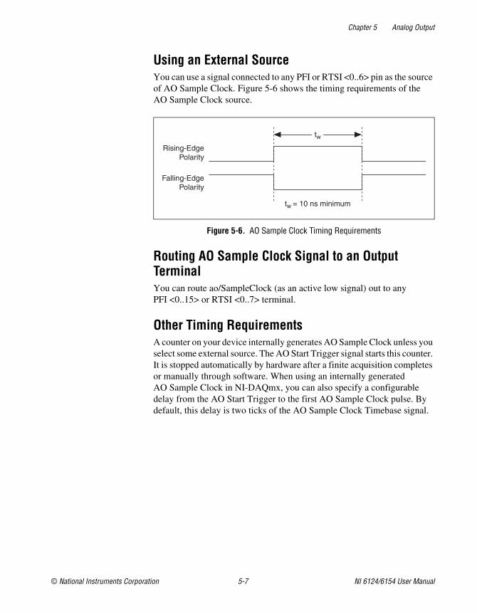
Chapter 5 Analog Output
© National Instruments Corporation 5-7 NI 6124/6154 User Manual
Using an External SourceYou can use a signal connected to any PFI or RTSI <0..6> pin as the source of AO Sample Clock. Figure 5-6 shows the timing requirements of the AO Sample Clock source.
Figure 5-6. AO Sample Clock Timing Requirements
Routing AO Sample Clock Signal to an Output TerminalYou can route ao/SampleClock (as an active low signal) out to any PFI <0..15> or RTSI <0..7> terminal.
Other Timing RequirementsA counter on your device internally generates AO Sample Clock unless you select some external source. The AO Start Trigger signal starts this counter. It is stopped automatically by hardware after a finite acquisition completes or manually through software. When using an internally generated AO Sample Clock in NI-DAQmx, you can also specify a configurable delay from the AO Start Trigger to the first AO Sample Clock pulse. By default, this delay is two ticks of the AO Sample Clock Timebase signal.
Rising-EdgePolarity
Falling-EdgePolarity
tw = 10 ns minimum
tw
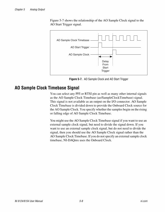
Chapter 5 Analog Output
NI 6124/6154 User Manual 5-8 ni.com
Figure 5-7 shows the relationship of the AO Sample Clock signal to the AO Start Trigger signal.
Figure 5-7. AO Sample Clock and AO Start Trigger
AO Sample Clock Timebase SignalYou can select any PFI or RTSI pin as well as many other internal signals as the AO Sample Clock Timebase (ao/SampleClockTimebase) signal. This signal is not available as an output on the I/O connector. AO Sample Clock Timebase is divided down to provide the Onboard Clock source for the AO Sample Clock. You specify whether the samples begin on the rising or falling edge of AO Sample Clock Timebase.
You might use the AO Sample Clock Timebase signal if you want to use an external sample clock signal, but need to divide the signal down. If you want to use an external sample clock signal, but do not need to divide the signal, then you should use the AO Sample Clock signal rather than the AO Sample Clock Timebase. If you do not specify an external sample clock timebase, NI-DAQmx uses the Onboard Clock.
AO Start Trigger
AO Sample Clock
AO Sample Clock Timebase
DelayFromStart
Trigger
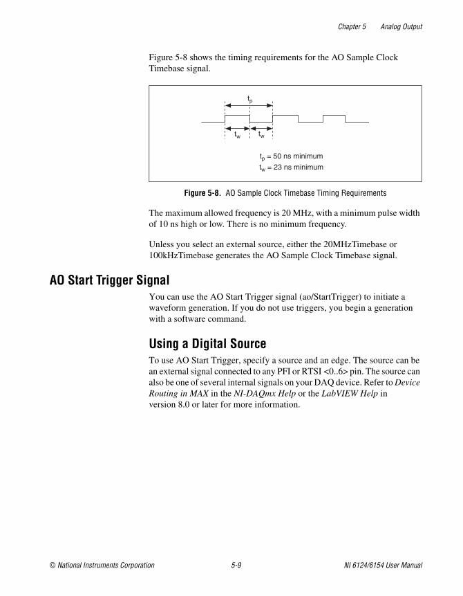
Chapter 5 Analog Output
© National Instruments Corporation 5-9 NI 6124/6154 User Manual
Figure 5-8 shows the timing requirements for the AO Sample Clock Timebase signal.
Figure 5-8. AO Sample Clock Timebase Timing Requirements
The maximum allowed frequency is 20 MHz, with a minimum pulse width of 10 ns high or low. There is no minimum frequency.
Unless you select an external source, either the 20MHzTimebase or 100kHzTimebase generates the AO Sample Clock Timebase signal.
AO Start Trigger SignalYou can use the AO Start Trigger signal (ao/StartTrigger) to initiate a waveform generation. If you do not use triggers, you begin a generation with a software command.
Using a Digital SourceTo use AO Start Trigger, specify a source and an edge. The source can be an external signal connected to any PFI or RTSI <0..6> pin. The source can also be one of several internal signals on your DAQ device. Refer to Device Routing in MAX in the NI-DAQmx Help or the LabVIEW Help in version 8.0 or later for more information.
tp = 50 ns minimum
tw = 23 ns minimum
tw tw
tp
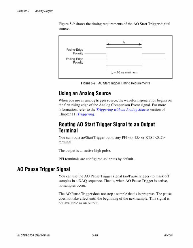
Chapter 5 Analog Output
NI 6124/6154 User Manual 5-10 ni.com
Figure 5-9 shows the timing requirements of the AO Start Trigger digital source.
Figure 5-9. AO Start Trigger Timing Requirements
Using an Analog SourceWhen you use an analog trigger source, the waveform generation begins on the first rising edge of the Analog Comparison Event signal. For more information, refer to the Triggering with an Analog Source section of Chapter 11, Triggering.
Routing AO Start Trigger Signal to an Output TerminalYou can route ao/StartTrigger out to any PFI <0..15> or RTSI <0..7> terminal.
The output is an active high pulse.
PFI terminals are configured as inputs by default.
AO Pause Trigger SignalYou can use the AO Pause Trigger signal (ao/PauseTrigger) to mask off samples in a DAQ sequence. That is, when AO Pause Trigger is active, no samples occur.
The AO Pause Trigger does not stop a sample that is in progress. The pause does not take effect until the beginning of the next sample. This signal is not available as an output.
Rising-EdgePolarity
Falling-EdgePolarity
tw
tw = 10 ns minimum
Chapter 5 Analog Output
© National Instruments Corporation 5-11 NI 6124/6154 User Manual
Using a Digital SourceTo use ao/Pause Trigger, specify a source and a polarity. The source can be an external signal connected to any PFI or RTSI <0..6> pin. The source can also be one of several other internal signals on your DAQ device. Refer to Device Routing in MAX in the NI-DAQmx Help or the LabVIEW Help in version 8.0 or later for more information.
Also, specify whether the samples are paused when AO Pause Trigger is at a logic high or low level.
Using an Analog SourceWhen you use an analog trigger source, the samples are paused when the Analog Comparison Event signal is at a high level. For more information, refer to the Triggering with an Analog Source section of Chapter 11, Triggering.
Getting Started with AO Applications in SoftwareYou can use the S Series device in the following analog output applications:
• Single-point generation
• Finite generation
• Continuous generation
• Waveform generation
You can perform these generations through DMA, interrupt, or programmed I/O data transfer mechanisms. Some of the applications also use start triggers and pause triggers.
Note For more information about programming analog output applications and triggers in software, refer to the NI-DAQmx Help or the LabVIEW Help in version 8.0 or later.
© National Instruments Corporation 6-1 NI 6124/6154 User Manual
6Digital I/O
Refer to one of the following sections, depending on your device:
• Digital I/O for Non-Isolated Devices—NI 6124 devices have eight lines of bidirectional DIO lines on Port 0, and 16 PFI signals that can function as static DIO lines.
• Digital I/O for Isolated Devices—NI 6154 devices have six bank-isolated digital inputs and four bank-isolated digital outputs.
Digital I/O for Non-Isolated Devices(NI 6124 Only) NI 6124 devices contain eight lines of bidirectional DIO lines on Port 0. In addition, The NI 6124 has 16 PFI lines that can function as static DIO lines.
These S Series devices support the following DIO features on Port 0:
• Eight lines of DIO
• Direction and function of each terminal individually controllable
• Static digital input and output
• High-speed digital waveform generation
• High-speed digital waveform acquisition
• DI change detection trigger/interrupt
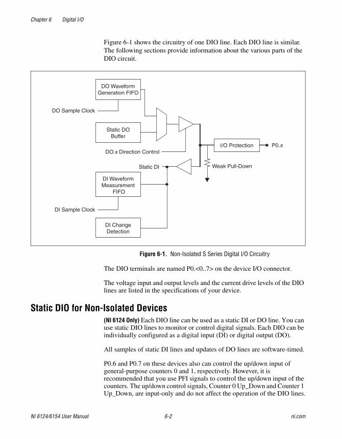
Chapter 6 Digital I/O
NI 6124/6154 User Manual 6-2 ni.com
Figure 6-1 shows the circuitry of one DIO line. Each DIO line is similar. The following sections provide information about the various parts of the DIO circuit.
Figure 6-1. Non-Isolated S Series Digital I/O Circuitry
The DIO terminals are named P0.<0..7> on the device I/O connector.
The voltage input and output levels and the current drive levels of the DIO lines are listed in the specifications of your device.
Static DIO for Non-Isolated Devices(NI 6124 Only) Each DIO line can be used as a static DI or DO line. You can use static DIO lines to monitor or control digital signals. Each DIO can be individually configured as a digital input (DI) or digital output (DO).
All samples of static DI lines and updates of DO lines are software-timed.
P0.6 and P0.7 on these devices also can control the up/down input of general-purpose counters 0 and 1, respectively. However, it is recommended that you use PFI signals to control the up/down input of the counters. The up/down control signals, Counter 0 Up_Down and Counter 1 Up_Down, are input-only and do not affect the operation of the DIO lines.
DO Sample Clock
DO WaveformGeneration FIFO
DO.x Direction Control
Static DI
DI Sample Clock
DI ChangeDetection
I/O Protection
Weak Pull-Down
P0.x
Static DOBuffer
DI WaveformMeasurement
FIFO
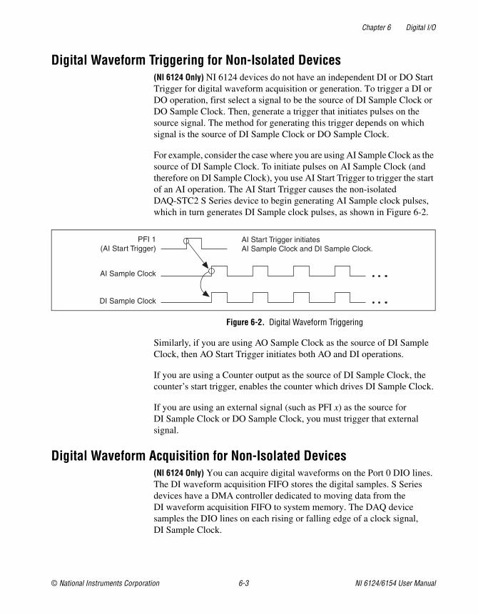
Chapter 6 Digital I/O
© National Instruments Corporation 6-3 NI 6124/6154 User Manual
Digital Waveform Triggering for Non-Isolated Devices(NI 6124 Only) NI 6124 devices do not have an independent DI or DO Start Trigger for digital waveform acquisition or generation. To trigger a DI or DO operation, first select a signal to be the source of DI Sample Clock or DO Sample Clock. Then, generate a trigger that initiates pulses on the source signal. The method for generating this trigger depends on which signal is the source of DI Sample Clock or DO Sample Clock.
For example, consider the case where you are using AI Sample Clock as the source of DI Sample Clock. To initiate pulses on AI Sample Clock (and therefore on DI Sample Clock), you use AI Start Trigger to trigger the start of an AI operation. The AI Start Trigger causes the non-isolated DAQ-STC2 S Series device to begin generating AI Sample clock pulses, which in turn generates DI Sample clock pulses, as shown in Figure 6-2.
Figure 6-2. Digital Waveform Triggering
Similarly, if you are using AO Sample Clock as the source of DI Sample Clock, then AO Start Trigger initiates both AO and DI operations.
If you are using a Counter output as the source of DI Sample Clock, the counter’s start trigger, enables the counter which drives DI Sample Clock.
If you are using an external signal (such as PFI x) as the source for DI Sample Clock or DO Sample Clock, you must trigger that external signal.
Digital Waveform Acquisition for Non-Isolated Devices(NI 6124 Only) You can acquire digital waveforms on the Port 0 DIO lines. The DI waveform acquisition FIFO stores the digital samples. S Series devices have a DMA controller dedicated to moving data from the DI waveform acquisition FIFO to system memory. The DAQ device samples the DIO lines on each rising or falling edge of a clock signal, DI Sample Clock.
PFI 1(AI Start Trigger)
AI Sample Clock
DI Sample Clock
AI Start Trigger initiates AI Sample Clock and DI Sample Clock.
Chapter 6 Digital I/O
NI 6124/6154 User Manual 6-4 ni.com
You can configure each DIO line to be an output, a static input, or a digital waveform acquisition input.
DI Sample Clock Signal(NI 6124 Only) Use the DI Sample Clock (di/SampleClock) signal to sample the P0.<0..7> terminals and store the result in the DI waveform acquisition FIFO. These S Series devices do not have the ability to divide down a timebase to produce an internal DI Sample Clock for digital waveform acquisition. Therefore, you must route an external signal or one of many internal signals from another subsystem to be the DI Sample Clock. For example, you can correlate digital and analog samples in time by sharing your AI Sample Clock or AO Sample Clock as the source of your DI Sample Clock. To sample a digital signal independent of an AI, AO, or DO operation, you can configure a counter to generate the desired DI Sample Clock or use an external signal as the source of the clock.
If the DAQ device receives a DI Sample Clock when the FIFO is full, it reports an overflow error to the host software.
Using an Internal SourceTo use DI Sample Clock with an internal source, specify the signal source and the polarity of the signal. The source can be any of the following signals:
• AI Sample Clock (ai/SampleClock)
• AI Convert Clock (ai/ConvertClock)
• AO Sample Clock (ao/SampleClock)
• Counter n Internal Output
• Frequency Output
• DI Change Detection Output
Several other internal signals can be routed to DI Sample Clock through RTSI. Refer to Device Routing in MAX in the NI-DAQmx Help or the LabVIEW Help in version 8.0 or later for more information.
Using an External SourceYou can route any of the following signals as DI Sample Clock:
• PFI <0..15>
• RTSI <0..7>
Chapter 6 Digital I/O
© National Instruments Corporation 6-5 NI 6124/6154 User Manual
• PXI_STAR
• Analog Comparison Event (an analog trigger)
You can sample data on the rising or falling edge of DI Sample Clock.
Routing DI Sample Clock to an Output TerminalYou can route DI Sample Clock out to any PFI terminal. The PFI circuitry inverts the polarity of DI Sample Clock before driving the PFI terminal.
Digital Waveform Generation for Non-Isolated Devices(NI 6124 Only) You can generate digital waveforms on the Port 0 DIO lines. The DO waveform generation FIFO stores the digital samples. These S Series devices have a DMA controller dedicated to moving data from the system memory to the DO waveform generation FIFO. The DAQ device moves samples from the FIFO to the DIO terminals on each rising or falling edge of a clock signal, DO Sample Clock. You can configure each DIO signal to be an input, a static output, or a digital waveform generation output.
The FIFO supports a retransmit mode. In the retransmit mode, after all the samples in the FIFO have been clocked out, the FIFO begins outputting all of the samples again in the same order. For example, if the FIFO contains five samples, the pattern generated consists of sample #1, #2, #3, #4, #5, #1, #2, #3, #4, #5, #1, and so on.
DO Sample Clock Signal(NI 6124 Only) Use the DO Sample Clock (do/SampleClock) signal to update the DO terminals with the next sample from the DO waveform generation FIFO. These S Series devices do not have the ability to divide down a timebase to produce an internal DO Sample Clock for digital waveform generation. Therefore, you must route an external signal or one of many internal signals from another subsystem to be the DO Sample Clock. For example, you can correlate digital and analog samples in time by sharing your AI Sample Clock or AO Sample Clock as the source of your DO Sample Clock. To generate digital data independent of an AI, AO, or DI operation, you can configure a counter to generate the desired DO Sample Clock or use an external signal as the source of the clock.
If the DAQ device receives a DO Sample Clock when the FIFO is empty, the DAQ device reports an underflow error to the host software.
Chapter 6 Digital I/O
NI 6124/6154 User Manual 6-6 ni.com
Using an Internal SourceTo use DO Sample Clock with an internal source, specify the signal source and the polarity of the signal. The source can be any of the following signals:
• AI Sample Clock (ai/SampleClock)
• AI Convert Clock (ai/ConvertClock)
• AO Sample Clock (ao/SampleClock)
• Counter n Internal Output
• Frequency Output
• DI Change Detection Output
Several other internal signals can be routed to DO Sample Clock through RTSI. Refer to Device Routing in MAX in the NI-DAQmx Help or the LabVIEW Help in version 8.0 or later for more information.
Using an External SourceYou can route any of the following signals as DO Sample Clock:
• PFI <0..15>
• RTSI <0..7>
• PXI_STAR
• Analog Comparison Event (an analog trigger)
You can generate samples on the rising or falling edge of DO Sample Clock.
You must ensure that the time between two active edges of DO Sample Clock is not too short. If the time is too short, the DO waveform generation FIFO is not able to read the next sample fast enough. The DAQ device reports an overrun error to the host software.
Routing DO Sample Clock to an Output TerminalYou can route DO Sample Clock out to any PFI terminal. The PFI circuitry inverts the polarity of DO Sample Clock before driving the PFI terminal.
Chapter 6 Digital I/O
© National Instruments Corporation 6-7 NI 6124/6154 User Manual
I/O Protection for Non-Isolated Devices(NI 6124 Only) Each DIO and PFI signal is protected against overvoltage, undervoltage, and overcurrent conditions as well as ESD events. However, you should avoid these fault conditions by following these guidelines:
• If you configure a PFI or DIO line as an output, do not connect it to any external signal source, ground, or power supply.
• If you configure a PFI or DIO line as an output, understand the current requirements of the load connected to these signals. Do not exceed the specified current output limits of the DAQ device. NI has several signal conditioning solutions for digital applications requiring high current drive.
• If you configure a PFI or DIO line as an input, do not drive the line with voltages outside of its normal operating range. The PFI or DIO lines have a smaller operating range than the AI signals.
• Treat the DAQ device as you would treat any static sensitive device. Always properly ground yourself and the equipment when handling the DAQ device or connecting to it.
Programmable Power-Up States for Non-Isolated Devices(NI 6124 Only) At system startup and reset, the hardware sets all PFI and DIO lines to high-impedance inputs by default. The DAQ device does not drive the signal high or low. Each line has a weak pull-down resistor connected to it, as described in the specifications document for your device.
NI-DAQmx supports programmable power-up states for PFI and DIO lines. Software can program any value at power up to the P0, P1, or P2 lines. The PFI and DIO lines can be set as:
• A high-impedance input with a weak pull-down resistor (default)
• An output driving a 0
• An output driving a 1
Refer to the NI-DAQmx Help or the LabVIEW Help in version 8.0 or later for more information about setting power-up states in NI-DAQmx or MAX.
Note When using your S Series device to control an SCXI chassis, DIO lines 0, 1, 2, and 4 are used as communication lines and must be left to power-up in the default high-impedance state to avoid potential damage to these signals.
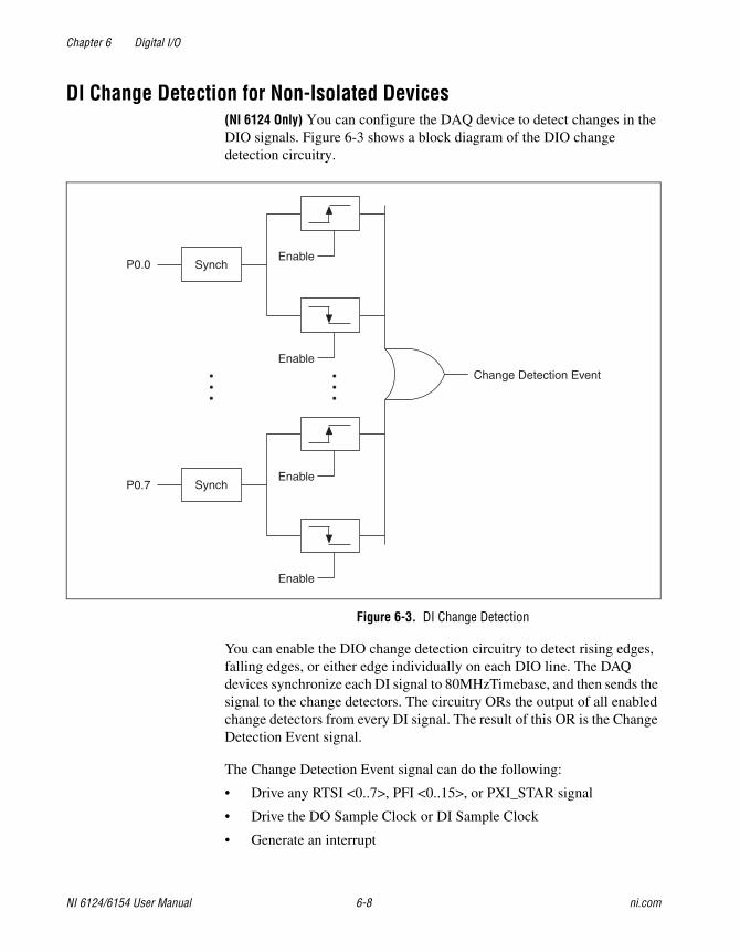
Chapter 6 Digital I/O
NI 6124/6154 User Manual 6-8 ni.com
DI Change Detection for Non-Isolated Devices(NI 6124 Only) You can configure the DAQ device to detect changes in the DIO signals. Figure 6-3 shows a block diagram of the DIO change detection circuitry.
Figure 6-3. DI Change Detection
You can enable the DIO change detection circuitry to detect rising edges, falling edges, or either edge individually on each DIO line. The DAQ devices synchronize each DI signal to 80MHzTimebase, and then sends the signal to the change detectors. The circuitry ORs the output of all enabled change detectors from every DI signal. The result of this OR is the Change Detection Event signal.
The Change Detection Event signal can do the following:
• Drive any RTSI <0..7>, PFI <0..15>, or PXI_STAR signal
• Drive the DO Sample Clock or DI Sample Clock
• Generate an interrupt
Synch
Synch
P0.0
P0.7
Enable
Enable
Enable
Enable
Change Detection Event
Chapter 6 Digital I/O
© National Instruments Corporation 6-9 NI 6124/6154 User Manual
The Change Detection Event signal also can be used to detect changes on digital output events.
DI Change Detection Applications for Non-Isolated Devices(NI 6124 Only) The DIO change detection circuitry can interrupt a user program when one of several DIO signals changes state.
You also can use the output of the DIO change detection circuitry to trigger a DI or counter acquisition on the logical OR of several digital signals. To trigger on a single digital signal, refer to the Triggering with a Digital Source section of Chapter 11, Triggering. By routing the Change Detection Event signal to a counter, you also can capture the relative time between samples.
You also can use the Change Detection Event signal to trigger DO or counter generations.
Connecting Digital I/O Signals on Non-Isolated Devices(NI 6124 Only) The DIO signals, P0.<0..7>, PFI <0..7>/P1.<0..7>, and PFI <8..15>/P2.<0..7> are referenced to D GND. You can individually program each line as an input or output. Figure 6-4 shows PFI <0..3>/P1.<0..3> configured for digital input and PFI <4..7>/P1.<4..7> configured for digital output. Digital input applications include receiving TTL signals and sensing external device states, such as the state of the switch shown in the figure. Digital output applications include sending TTL signals and driving external devices, such as the LED shown in the figure.
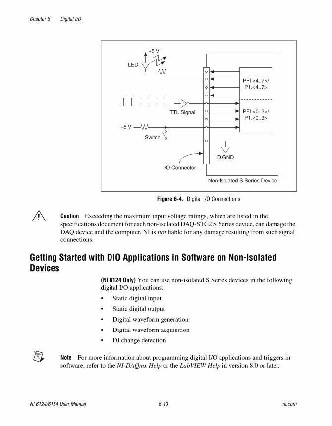
Chapter 6 Digital I/O
NI 6124/6154 User Manual 6-10 ni.com
Figure 6-4. Digital I/O Connections
Caution Exceeding the maximum input voltage ratings, which are listed in the specifications document for each non-isolated DAQ-STC2 S Series device, can damage the DAQ device and the computer. NI is not liable for any damage resulting from such signal connections.
Getting Started with DIO Applications in Software on Non-Isolated Devices
(NI 6124 Only) You can use non-isolated S Series devices in the following digital I/O applications:
• Static digital input
• Static digital output
• Digital waveform generation
• Digital waveform acquisition
• DI change detection
Note For more information about programming digital I/O applications and triggers in software, refer to the NI-DAQmx Help or the LabVIEW Help in version 8.0 or later.
+5 V
LED
TTL Signal
+5 V
Switch
I/O Connector
D GND
Non-Isolated S Series Device
PFI <0..3>/P1.<0..3>
PFI <4..7>/P1.<4..7>
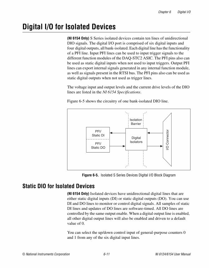
Chapter 6 Digital I/O
© National Instruments Corporation 6-11 NI 6124/6154 User Manual
Digital I/O for Isolated Devices(NI 6154 Only) S Series isolated devices contain ten lines of unidirectional DIO signals. The digital I/O port is comprised of six digital inputs and four digital outputs, all bank-isolated. Each digital line has the functionality of a PFI line. Input PFI lines can be used to input trigger signals to the different function modules of the DAQ-STC2 ASIC. The PFI pins also can be used as static digital inputs when not used to input triggers. Output PFI lines can export internal signals generated in any internal function module, as well as signals present in the RTSI bus. The PFI pins also can be used as static digital outputs when not used as trigger lines.
The voltage input and output levels and the current drive levels of the DIO lines are listed in the NI 6154 Specifications.
Figure 6-5 shows the circuitry of one bank-isolated DIO line.
Figure 6-5. Isolated S Series Devices Digital I/O Block Diagram
Static DIO for Isolated Devices(NI 6154 Only) Isolated devices have unidirectional digital lines that are either static digital inputs (DI) or static digital outputs (DO). You can use DI and DO lines to monitor or control digital signals. All samples of static DI lines and updates of DO lines are software-timed. All DO lines are controlled by the same output enable. When a digital output line is enabled, all other digital output lines will also be enabled and driven to a default value of 0.
You can select the up/down control input of general-purpose counters 0 and 1 from any of the six digital input lines.
IsolationBarrier
DigitalIsolators
PFI/Static DI
I/O C
onne
ctor
PFI/Static DO
Chapter 6 Digital I/O
NI 6124/6154 User Manual 6-12 ni.com
I/O Protection for Isolated Devices(NI 6154 Only) Each DIO and PFI signal is protected against over-voltage, under-voltage, and over-current conditions as well as ESD events. However, you should avoid these fault conditions by following these guidelines:
• Do not connect any DO line to any external signal source, ground signal, or power supply.
• Understand the current requirements of the load connected to DO signals. Do not exceed the specified current output limits of the DAQ device. NI has several signal conditioning solutions for digital applications requiring high-current drive.
• Do not drive any DI line with voltages outside of its normal operating range. The PFI or DIO lines have a smaller operating range than the AI signals.
• Treat the DAQ device as you would treat any static sensitive device. Always properly ground yourself and the equipment when handling the DAQ device or connecting to it.
Connecting Digital I/O Signals on Isolated Devices(NI 6154 Only) The DIO signals, PFI <0..5>/P0.<0..5> and PFI <6..9>/P1.<0..3>, are referenced to D GND. PFI <0..5>/P0.<0..5> are inputs and PFI <6..9>/P1.<0..3> are outputs. Figure 6-6 shows digital inputs PFI <0..5>/P0.<0..5> and digital outputs PFI <6..9>/P1.<0..3>. Digital input applications include receiving TTL signals and sensing external device states, such as the state of the switch shown in the figure. Digital output applications include sending TTL signals and driving external devices, such as the LED shown in Figure 6-6.
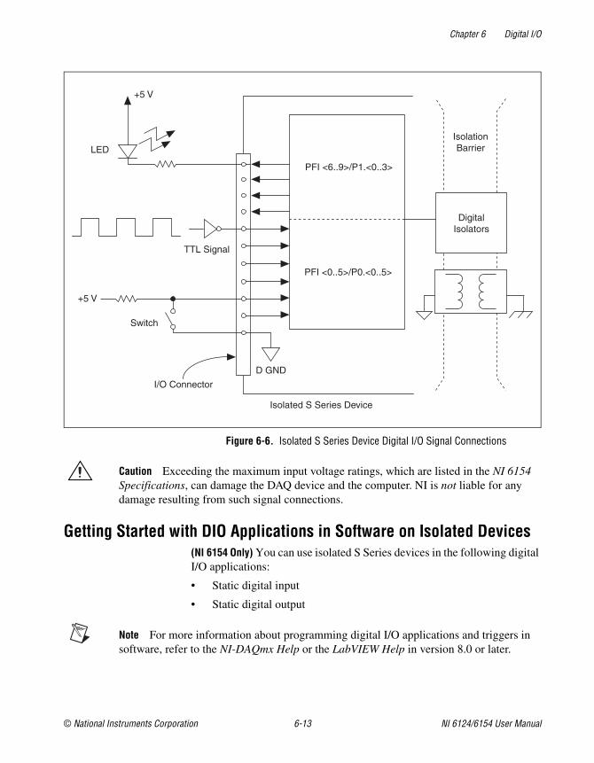
Chapter 6 Digital I/O
© National Instruments Corporation 6-13 NI 6124/6154 User Manual
Figure 6-6. Isolated S Series Device Digital I/O Signal Connections
Caution Exceeding the maximum input voltage ratings, which are listed in the NI 6154 Specifications, can damage the DAQ device and the computer. NI is not liable for any damage resulting from such signal connections.
Getting Started with DIO Applications in Software on Isolated Devices(NI 6154 Only) You can use isolated S Series devices in the following digital I/O applications:
• Static digital input
• Static digital output
Note For more information about programming digital I/O applications and triggers in software, refer to the NI-DAQmx Help or the LabVIEW Help in version 8.0 or later.
Isolated S Series Device
+5 V
LED
TTL Signal
+5 V
Switch
I/O Connector
D GND
PFI <0..5>/P0.<0..5>
PFI <6..9>/P1.<0..3>
DigitalIsolators
IsolationBarrier
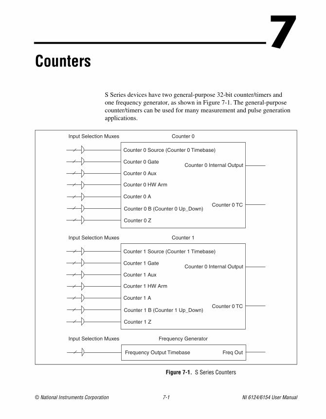
© National Instruments Corporation 7-1 NI 6124/6154 User Manual
7Counters
S Series devices have two general-purpose 32-bit counter/timers and one frequency generator, as shown in Figure 7-1. The general-purpose counter/timers can be used for many measurement and pulse generation applications.
Figure 7-1. S Series Counters
Counter 0
Counter 0 Source (Counter 0 Timebase)
Counter 0 Aux
Counter 0 HW Arm
Counter 0 A
Counter 0 B (Counter 0 Up_Down)
Counter 0 Z
Counter 0 Gate Counter 0 Internal Output
Counter 0 TC
Input Selection Muxes
Frequency Generator
Frequency Output Timebase Freq Out
Input Selection Muxes
Counter 1
Counter 1 Source (Counter 1 Timebase)
Counter 1 Aux
Counter 1 HW Arm
Counter 1 A
Counter 1 B (Counter 1 Up_Down)
Counter 1 Z
Counter 1 Gate Counter 0 Internal Output
Counter 0 TC
Input Selection Muxes
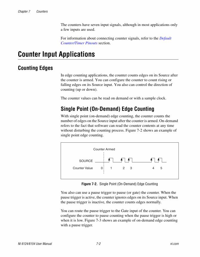
Chapter 7 Counters
NI 6124/6154 User Manual 7-2 ni.com
The counters have seven input signals, although in most applications only a few inputs are used.
For information about connecting counter signals, refer to the Default Counter/Timer Pinouts section.
Counter Input Applications
Counting EdgesIn edge counting applications, the counter counts edges on its Source after the counter is armed. You can configure the counter to count rising or falling edges on its Source input. You also can control the direction of counting (up or down).
The counter values can be read on demand or with a sample clock.
Single Point (On-Demand) Edge CountingWith single point (on-demand) edge counting, the counter counts the number of edges on the Source input after the counter is armed. On-demand refers to the fact that software can read the counter contents at any time without disturbing the counting process. Figure 7-2 shows an example of single point edge counting.
Figure 7-2. Single Point (On-Demand) Edge Counting
You also can use a pause trigger to pause (or gate) the counter. When the pause trigger is active, the counter ignores edges on its Source input. When the pause trigger is inactive, the counter counts edges normally.
You can route the pause trigger to the Gate input of the counter. You can configure the counter to pause counting when the pause trigger is high or when it is low. Figure 7-3 shows an example of on-demand edge counting with a pause trigger.
Counter Armed
SOURCE
Counter Value 1 0 5 4 3 2
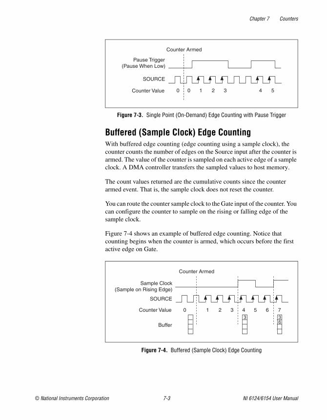
Chapter 7 Counters
© National Instruments Corporation 7-3 NI 6124/6154 User Manual
Figure 7-3. Single Point (On-Demand) Edge Counting with Pause Trigger
Buffered (Sample Clock) Edge CountingWith buffered edge counting (edge counting using a sample clock), the counter counts the number of edges on the Source input after the counter is armed. The value of the counter is sampled on each active edge of a sample clock. A DMA controller transfers the sampled values to host memory.
The count values returned are the cumulative counts since the counter armed event. That is, the sample clock does not reset the counter.
You can route the counter sample clock to the Gate input of the counter. You can configure the counter to sample on the rising or falling edge of the sample clock.
Figure 7-4 shows an example of buffered edge counting. Notice that counting begins when the counter is armed, which occurs before the first active edge on Gate.
Figure 7-4. Buffered (Sample Clock) Edge Counting
Counter Armed
SOURCE
Pause Trigger (Pause When Low)
Counter Value 1 0 0 5 4 3 2
3 6
3
Counter Armed
SOURCE
Sample Clock (Sample on Rising Edge)
Counter Value
Buffer
1 0 7 6 3 4 5 2
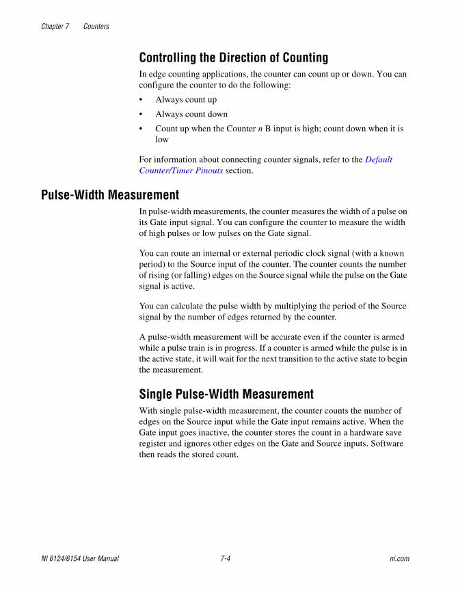
Chapter 7 Counters
NI 6124/6154 User Manual 7-4 ni.com
Controlling the Direction of CountingIn edge counting applications, the counter can count up or down. You can configure the counter to do the following:
• Always count up
• Always count down
• Count up when the Counter n B input is high; count down when it is low
For information about connecting counter signals, refer to the Default Counter/Timer Pinouts section.
Pulse-Width MeasurementIn pulse-width measurements, the counter measures the width of a pulse on its Gate input signal. You can configure the counter to measure the width of high pulses or low pulses on the Gate signal.
You can route an internal or external periodic clock signal (with a known period) to the Source input of the counter. The counter counts the number of rising (or falling) edges on the Source signal while the pulse on the Gate signal is active.
You can calculate the pulse width by multiplying the period of the Source signal by the number of edges returned by the counter.
A pulse-width measurement will be accurate even if the counter is armed while a pulse train is in progress. If a counter is armed while the pulse is in the active state, it will wait for the next transition to the active state to begin the measurement.
Single Pulse-Width MeasurementWith single pulse-width measurement, the counter counts the number of edges on the Source input while the Gate input remains active. When the Gate input goes inactive, the counter stores the count in a hardware save register and ignores other edges on the Gate and Source inputs. Software then reads the stored count.
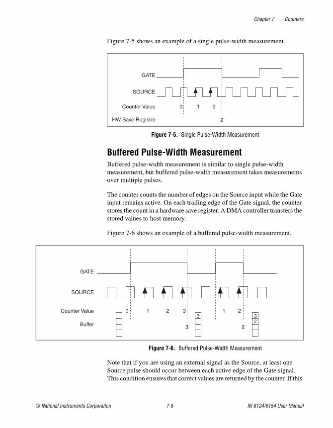
Chapter 7 Counters
© National Instruments Corporation 7-5 NI 6124/6154 User Manual
Figure 7-5 shows an example of a single pulse-width measurement.
Figure 7-5. Single Pulse-Width Measurement
Buffered Pulse-Width MeasurementBuffered pulse-width measurement is similar to single pulse-width measurement, but buffered pulse-width measurement takes measurements over multiple pulses.
The counter counts the number of edges on the Source input while the Gate input remains active. On each trailing edge of the Gate signal, the counter stores the count in a hardware save register. A DMA controller transfers the stored values to host memory.
Figure 7-6 shows an example of a buffered pulse-width measurement.
Figure 7-6. Buffered Pulse-Width Measurement
Note that if you are using an external signal as the Source, at least one Source pulse should occur between each active edge of the Gate signal. This condition ensures that correct values are returned by the counter. If this
SOURCE
GATE
Counter Value
HW Save Register
1 0
2
2
SOURCE
GATE
Counter Value
Buffer
10 3
3 2
2123 3
2
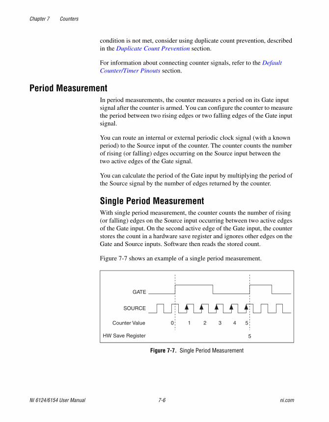
Chapter 7 Counters
NI 6124/6154 User Manual 7-6 ni.com
condition is not met, consider using duplicate count prevention, described in the Duplicate Count Prevention section.
For information about connecting counter signals, refer to the Default Counter/Timer Pinouts section.
Period MeasurementIn period measurements, the counter measures a period on its Gate input signal after the counter is armed. You can configure the counter to measure the period between two rising edges or two falling edges of the Gate input signal.
You can route an internal or external periodic clock signal (with a known period) to the Source input of the counter. The counter counts the number of rising (or falling) edges occurring on the Source input between the two active edges of the Gate signal.
You can calculate the period of the Gate input by multiplying the period of the Source signal by the number of edges returned by the counter.
Single Period MeasurementWith single period measurement, the counter counts the number of rising (or falling) edges on the Source input occurring between two active edges of the Gate input. On the second active edge of the Gate input, the counter stores the count in a hardware save register and ignores other edges on the Gate and Source inputs. Software then reads the stored count.
Figure 7-7 shows an example of a single period measurement.
Figure 7-7. Single Period Measurement
SOURCE
GATE
Counter Value
HW Save Register
1 0 3
5
4 5 2
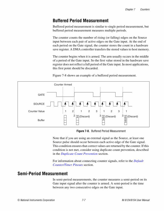
Chapter 7 Counters
© National Instruments Corporation 7-7 NI 6124/6154 User Manual
Buffered Period MeasurementBuffered period measurement is similar to single period measurement, but buffered period measurement measures multiple periods.
The counter counts the number of rising (or falling) edges on the Source input between each pair of active edges on the Gate input. At the end of each period on the Gate signal, the counter stores the count in a hardware save register. A DMA controller transfers the stored values to host memory.
The counter begins when it is armed. The arm usually occurs in the middle of a period of the Gate input. So the first value stored in the hardware save register does not reflect a full period of the Gate input. In most applications, this first point should be discarded.
Figure 7-8 shows an example of a buffered period measurement.
Figure 7-8. Buffered Period Measurement
Note that if you are using an external signal as the Source, at least one Source pulse should occur between each active edge of the Gate signal. This condition ensures that correct values are returned by the counter. If this condition is not met, consider using duplicate count prevention, described in the Duplicate Count Prevention section.
For information about connecting counter signals, refer to the Default Counter/Timer Pinouts section.
Semi-Period MeasurementIn semi-period measurements, the counter measures a semi-period on its Gate input signal after the counter is armed. A semi-period is the time between any two consecutive edges on the Gate input.
SOURCE
GATE
Counter Value
Buffer
1 1 2 3
3 2 3
3 1 1 2 2
2 2 3 3
2 (Discard) (Discard) (Discard) 3
Counter Armed
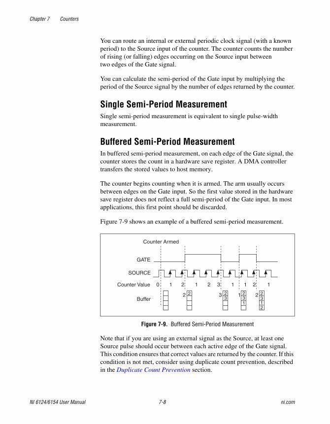
Chapter 7 Counters
NI 6124/6154 User Manual 7-8 ni.com
You can route an internal or external periodic clock signal (with a known period) to the Source input of the counter. The counter counts the number of rising (or falling) edges occurring on the Source input between two edges of the Gate signal.
You can calculate the semi-period of the Gate input by multiplying the period of the Source signal by the number of edges returned by the counter.
Single Semi-Period MeasurementSingle semi-period measurement is equivalent to single pulse-width measurement.
Buffered Semi-Period MeasurementIn buffered semi-period measurement, on each edge of the Gate signal, the counter stores the count in a hardware save register. A DMA controller transfers the stored values to host memory.
The counter begins counting when it is armed. The arm usually occurs between edges on the Gate input. So the first value stored in the hardware save register does not reflect a full semi-period of the Gate input. In most applications, this first point should be discarded.
Figure 7-9 shows an example of a buffered semi-period measurement.
Figure 7-9. Buffered Semi-Period Measurement
Note that if you are using an external signal as the Source, at least one Source pulse should occur between each active edge of the Gate signal. This condition ensures that correct values are returned by the counter. If this condition is not met, consider using duplicate count prevention, described in the Duplicate Count Prevention section.
3 1 2
2 3 1
2 2 3
2
SOURCE
GATE
Counter Value
Buffer
1 3
2
2 1 1
132
1 2 1 0 2
Counter Armed
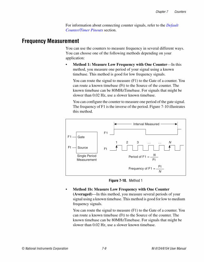
Chapter 7 Counters
© National Instruments Corporation 7-9 NI 6124/6154 User Manual
For information about connecting counter signals, refer to the Default Counter/Timer Pinouts section.
Frequency MeasurementYou can use the counters to measure frequency in several different ways. You can choose one of the following methods depending on your application:
• Method 1: Measure Low Frequency with One Counter—In this method, you measure one period of your signal using a known timebase. This method is good for low frequency signals.
You can route the signal to measure (F1) to the Gate of a counter. You can route a known timebase (Ft) to the Source of the counter. The known timebase can be 80MHzTimebase. For signals that might be slower than 0.02 Hz, use a slower known timebase.
You can configure the counter to measure one period of the gate signal. The frequency of F1 is the inverse of the period. Figure 7-10 illustrates this method.
Figure 7-10. Method 1
• Method 1b: Measure Low Frequency with One Counter (Averaged)—In this method, you measure several periods of your signal using a known timebase. This method is good for low to medium frequency signals.
You can route the signal to measure (F1) to the Gate of a counter. You can route a known timebase (Ft) to the Source of the counter. The known timebase can be 80MHzTimebase. For signals that might be slower than 0.02 Hz, use a slower known timebase.
F1
Ft
F1
Ft
Gate
Source
1 2 3 … N
Single PeriodMeasurement
…
Period of F1 = N
Ft
Frequency of F1 =N
Ft
Interval Measured
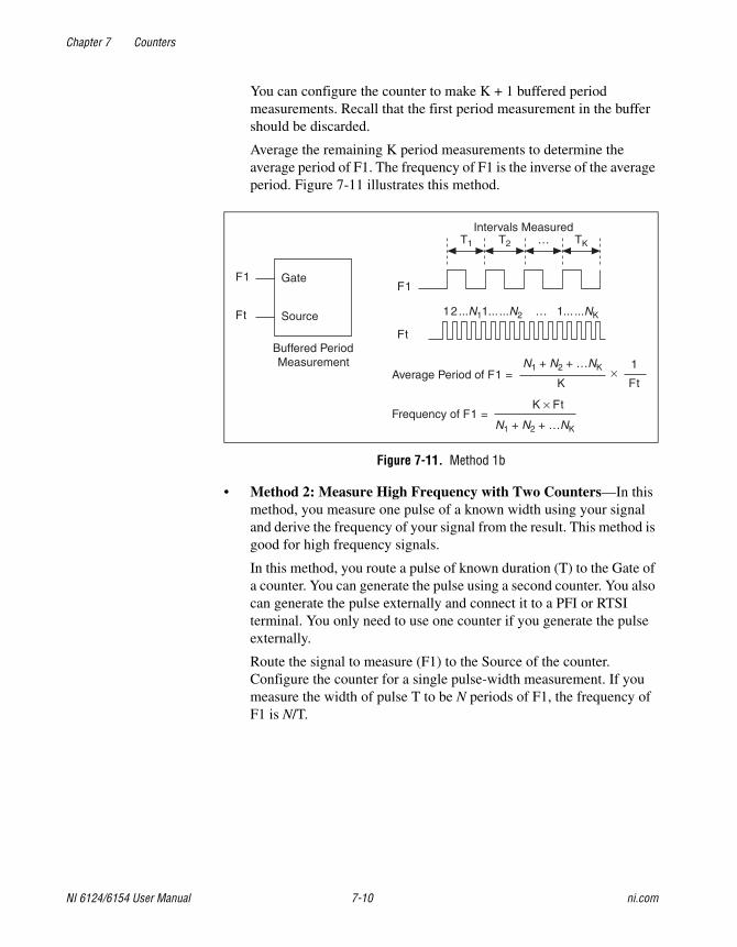
Chapter 7 Counters
NI 6124/6154 User Manual 7-10 ni.com
You can configure the counter to make K + 1 buffered period measurements. Recall that the first period measurement in the buffer should be discarded.
Average the remaining K period measurements to determine the average period of F1. The frequency of F1 is the inverse of the average period. Figure 7-11 illustrates this method.
Figure 7-11. Method 1b
• Method 2: Measure High Frequency with Two Counters—In this method, you measure one pulse of a known width using your signal and derive the frequency of your signal from the result. This method is good for high frequency signals.
In this method, you route a pulse of known duration (T) to the Gate of a counter. You can generate the pulse using a second counter. You also can generate the pulse externally and connect it to a PFI or RTSI terminal. You only need to use one counter if you generate the pulse externally.
Route the signal to measure (F1) to the Source of the counter. Configure the counter for a single pulse-width measurement. If you measure the width of pulse T to be N periods of F1, the frequency of F1 is N/T.
F1
Ft
F1
Intervals Measured
Gate
Source
Buffered Period Measurement
Average Period of F1 = N1 + N2 + …NK
K
Frequency of F1 = N1 + N2 + …NK
K × Ft
Ft
T1 T2 … TK
1
Ft ×
1 2 ...N11... ...N2 … 1... ...NK
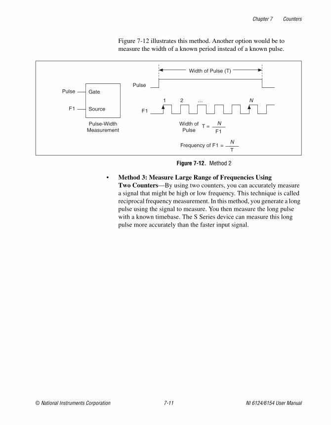
Chapter 7 Counters
© National Instruments Corporation 7-11 NI 6124/6154 User Manual
Figure 7-12 illustrates this method. Another option would be to measure the width of a known period instead of a known pulse.
Figure 7-12. Method 2
• Method 3: Measure Large Range of Frequencies Using Two Counters—By using two counters, you can accurately measure a signal that might be high or low frequency. This technique is called reciprocal frequency measurement. In this method, you generate a long pulse using the signal to measure. You then measure the long pulse with a known timebase. The S Series device can measure this long pulse more accurately than the faster input signal.
Pulse
F1
Pulse
F1
Gate
Source
1 2 … N
Pulse-Width Measurement
T = N
F1
Frequency of F1 = T
Width of Pulse
N
Width of Pulse (T)
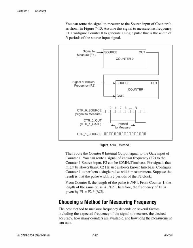
Chapter 7 Counters
NI 6124/6154 User Manual 7-12 ni.com
You can route the signal to measure to the Source input of Counter 0, as shown in Figure 7-13. Assume this signal to measure has frequency F1. Configure Counter 0 to generate a single pulse that is the width of N periods of the source input signal.
Figure 7-13. Method 3
Then route the Counter 0 Internal Output signal to the Gate input of Counter 1. You can route a signal of known frequency (F2) to the Counter 1 Source input. F2 can be 80MHzTimebase. For signals that might be slower than 0.02 Hz, use a slower known timebase. Configure Counter 1 to perform a single pulse-width measurement. Suppose the result is that the pulse width is J periods of the F2 clock.
From Counter 0, the length of the pulse is N/F1. From Counter 1, the length of the same pulse is J/F2. Therefore, the frequency of F1 is given by F1 = F2 * (N/J).
Choosing a Method for Measuring FrequencyThe best method to measure frequency depends on several factors including the expected frequency of the signal to measure, the desired accuracy, how many counters are available, and how long the measurement can take.
SOURCE OUT
COUNTER 0
SOURCE
GATE
OUT
COUNTER 1
Signal to Measure (F1)
Signal of Known Frequency (F2)
CTR_0_SOURCE (Signal to Measure)
CTR_0_OUT (CTR_1_GATE)
CTR_1_SOURCE
Interval to Measure
0 1 2 3 … N
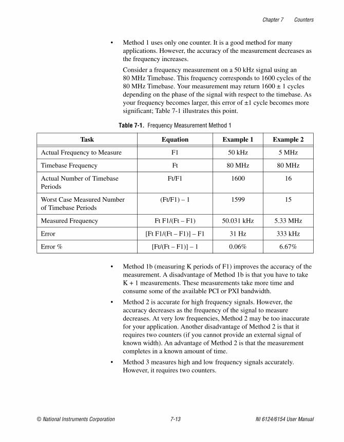
Chapter 7 Counters
© National Instruments Corporation 7-13 NI 6124/6154 User Manual
• Method 1 uses only one counter. It is a good method for many applications. However, the accuracy of the measurement decreases as the frequency increases.
Consider a frequency measurement on a 50 kHz signal using an 80 MHz Timebase. This frequency corresponds to 1600 cycles of the 80 MHz Timebase. Your measurement may return 1600 ± 1 cycles depending on the phase of the signal with respect to the timebase. As your frequency becomes larger, this error of ±1 cycle becomes more significant; Table 7-1 illustrates this point.
• Method 1b (measuring K periods of F1) improves the accuracy of the measurement. A disadvantage of Method 1b is that you have to take K + 1 measurements. These measurements take more time and consume some of the available PCI or PXI bandwidth.
• Method 2 is accurate for high frequency signals. However, the accuracy decreases as the frequency of the signal to measure decreases. At very low frequencies, Method 2 may be too inaccurate for your application. Another disadvantage of Method 2 is that it requires two counters (if you cannot provide an external signal of known width). An advantage of Method 2 is that the measurement completes in a known amount of time.
• Method 3 measures high and low frequency signals accurately. However, it requires two counters.
Table 7-1. Frequency Measurement Method 1
Task Equation Example 1 Example 2
Actual Frequency to Measure F1 50 kHz 5 MHz
Timebase Frequency Ft 80 MHz 80 MHz
Actual Number of Timebase Periods
Ft/F1 1600 16
Worst Case Measured Number of Timebase Periods
(Ft/F1) – 1 1599 15
Measured Frequency Ft F1/(Ft – F1) 50.031 kHz 5.33 MHz
Error [Ft F1/(Ft – F1)] – F1 31 Hz 333 kHz
Error % [Ft/(Ft – F1)] – 1 0.06% 6.67%
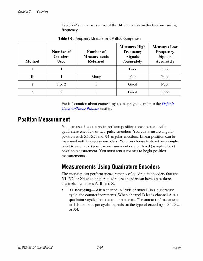
Chapter 7 Counters
NI 6124/6154 User Manual 7-14 ni.com
Table 7-2 summarizes some of the differences in methods of measuring frequency.
For information about connecting counter signals, refer to the Default Counter/Timer Pinouts section.
Position MeasurementYou can use the counters to perform position measurements with quadrature encoders or two-pulse encoders. You can measure angular position with X1, X2, and X4 angular encoders. Linear position can be measured with two-pulse encoders. You can choose to do either a single point (on-demand) position measurement or a buffered (sample clock) position measurement. You must arm a counter to begin position measurements.
Measurements Using Quadrature EncodersThe counters can perform measurements of quadrature encoders that use X1, X2, or X4 encoding. A quadrature encoder can have up to three channels—channels A, B, and Z.
• X1 Encoding—When channel A leads channel B in a quadrature cycle, the counter increments. When channel B leads channel A in a quadrature cycle, the counter decrements. The amount of increments and decrements per cycle depends on the type of encoding—X1, X2, or X4.
Table 7-2. Frequency Measurement Method Comparison
Method
Number of Counters
Used
Number of Measurements
Returned
Measures High Frequency
Signals Accurately
Measures Low Frequency
Signals Accurately
1 1 1 Poor Good
1b 1 Many Fair Good
2 1 or 2 1 Good Poor
3 2 1 Good Good
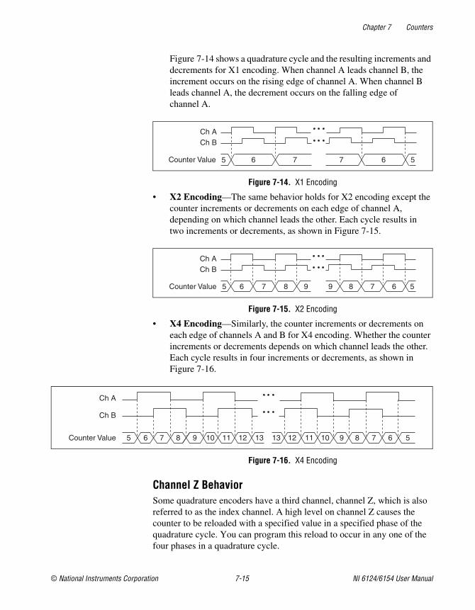
Chapter 7 Counters
© National Instruments Corporation 7-15 NI 6124/6154 User Manual
Figure 7-14 shows a quadrature cycle and the resulting increments and decrements for X1 encoding. When channel A leads channel B, the increment occurs on the rising edge of channel A. When channel B leads channel A, the decrement occurs on the falling edge of channel A.
Figure 7-14. X1 Encoding
• X2 Encoding—The same behavior holds for X2 encoding except the counter increments or decrements on each edge of channel A, depending on which channel leads the other. Each cycle results in two increments or decrements, as shown in Figure 7-15.
Figure 7-15. X2 Encoding
• X4 Encoding—Similarly, the counter increments or decrements on each edge of channels A and B for X4 encoding. Whether the counter increments or decrements depends on which channel leads the other. Each cycle results in four increments or decrements, as shown in Figure 7-16.
Figure 7-16. X4 Encoding
Channel Z BehaviorSome quadrature encoders have a third channel, channel Z, which is also referred to as the index channel. A high level on channel Z causes the counter to be reloaded with a specified value in a specified phase of the quadrature cycle. You can program this reload to occur in any one of the four phases in a quadrature cycle.
Ch A Ch B
Counter Value 7 7 6 5 5 6
Ch A Ch B
Counter Value 5 6 8 9 7 5 6 8 9 7
Ch A
Ch B
Counter Value 5 6 8 9 10 10 11 11 12 12 13 13 7 5 6 8 7 9
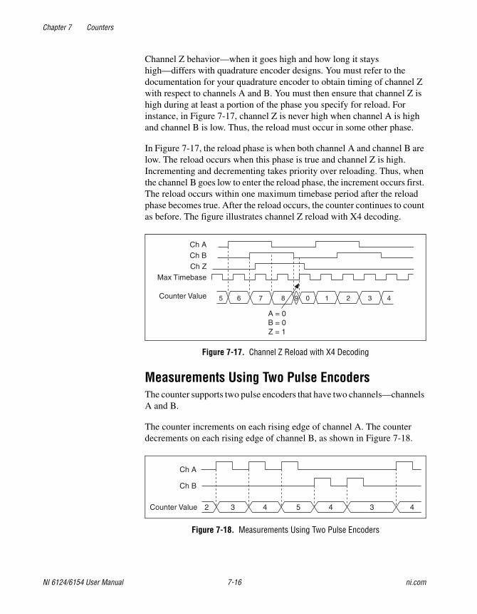
Chapter 7 Counters
NI 6124/6154 User Manual 7-16 ni.com
Channel Z behavior—when it goes high and how long it stays high—differs with quadrature encoder designs. You must refer to the documentation for your quadrature encoder to obtain timing of channel Z with respect to channels A and B. You must then ensure that channel Z is high during at least a portion of the phase you specify for reload. For instance, in Figure 7-17, channel Z is never high when channel A is high and channel B is low. Thus, the reload must occur in some other phase.
In Figure 7-17, the reload phase is when both channel A and channel B are low. The reload occurs when this phase is true and channel Z is high. Incrementing and decrementing takes priority over reloading. Thus, when the channel B goes low to enter the reload phase, the increment occurs first. The reload occurs within one maximum timebase period after the reload phase becomes true. After the reload occurs, the counter continues to count as before. The figure illustrates channel Z reload with X4 decoding.
Figure 7-17. Channel Z Reload with X4 Decoding
Measurements Using Two Pulse EncodersThe counter supports two pulse encoders that have two channels—channels A and B.
The counter increments on each rising edge of channel A. The counter decrements on each rising edge of channel B, as shown in Figure 7-18.
Figure 7-18. Measurements Using Two Pulse Encoders
Ch ACh B
Counter Value 5 6
A = 0 B = 0 Z = 1
Ch ZMax Timebase
8 9 0 2 1 7 4 3
Ch A
Ch B
Counter Value 2 3 5 4 3 4 4
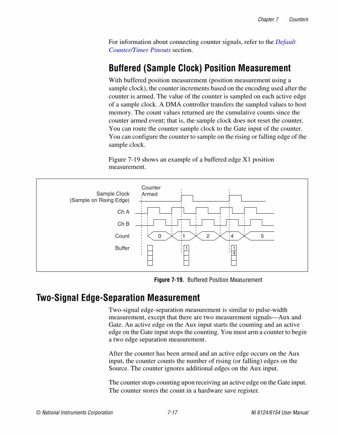
Chapter 7 Counters
© National Instruments Corporation 7-17 NI 6124/6154 User Manual
For information about connecting counter signals, refer to the Default Counter/Timer Pinouts section.
Buffered (Sample Clock) Position MeasurementWith buffered position measurement (position measurement using a sample clock), the counter increments based on the encoding used after the counter is armed. The value of the counter is sampled on each active edge of a sample clock. A DMA controller transfers the sampled values to host memory. The count values returned are the cumulative counts since the counter armed event; that is, the sample clock does not reset the counter. You can route the counter sample clock to the Gate input of the counter. You can configure the counter to sample on the rising or falling edge of the sample clock.
Figure 7-19 shows an example of a buffered edge X1 position measurement.
Figure 7-19. Buffered Position Measurement
Two-Signal Edge-Separation MeasurementTwo-signal edge-separation measurement is similar to pulse-width measurement, except that there are two measurement signals—Aux and Gate. An active edge on the Aux input starts the counting and an active edge on the Gate input stops the counting. You must arm a counter to begin a two edge separation measurement.
After the counter has been armed and an active edge occurs on the Aux input, the counter counts the number of rising (or falling) edges on the Source. The counter ignores additional edges on the Aux input.
The counter stops counting upon receiving an active edge on the Gate input. The counter stores the count in a hardware save register.
14
1
Ch A
Ch B
410 2 5Count
Buffer
Sample Clock(Sample on Rising Edge)
CounterArmed
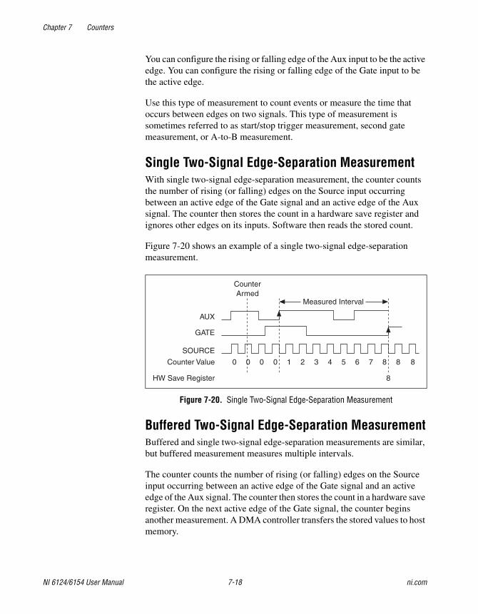
Chapter 7 Counters
NI 6124/6154 User Manual 7-18 ni.com
You can configure the rising or falling edge of the Aux input to be the active edge. You can configure the rising or falling edge of the Gate input to be the active edge.
Use this type of measurement to count events or measure the time that occurs between edges on two signals. This type of measurement is sometimes referred to as start/stop trigger measurement, second gate measurement, or A-to-B measurement.
Single Two-Signal Edge-Separation MeasurementWith single two-signal edge-separation measurement, the counter counts the number of rising (or falling) edges on the Source input occurring between an active edge of the Gate signal and an active edge of the Aux signal. The counter then stores the count in a hardware save register and ignores other edges on its inputs. Software then reads the stored count.
Figure 7-20 shows an example of a single two-signal edge-separation measurement.
Figure 7-20. Single Two-Signal Edge-Separation Measurement
Buffered Two-Signal Edge-Separation MeasurementBuffered and single two-signal edge-separation measurements are similar, but buffered measurement measures multiple intervals.
The counter counts the number of rising (or falling) edges on the Source input occurring between an active edge of the Gate signal and an active edge of the Aux signal. The counter then stores the count in a hardware save register. On the next active edge of the Gate signal, the counter begins another measurement. A DMA controller transfers the stored values to host memory.
AUX
Counter Armed
8
0 0 0 0 1 2 3 4 5 6 7 8 8 8
Measured Interval
GATE
SOURCE
Counter Value
HW Save Register
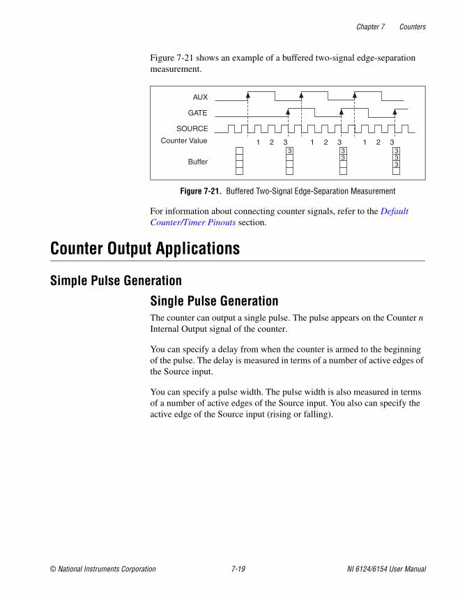
Chapter 7 Counters
© National Instruments Corporation 7-19 NI 6124/6154 User Manual
Figure 7-21 shows an example of a buffered two-signal edge-separation measurement.
Figure 7-21. Buffered Two-Signal Edge-Separation Measurement
For information about connecting counter signals, refer to the Default Counter/Timer Pinouts section.
Counter Output Applications
Simple Pulse Generation
Single Pulse GenerationThe counter can output a single pulse. The pulse appears on the Counter n Internal Output signal of the counter.
You can specify a delay from when the counter is armed to the beginning of the pulse. The delay is measured in terms of a number of active edges of the Source input.
You can specify a pulse width. The pulse width is also measured in terms of a number of active edges of the Source input. You also can specify the active edge of the Source input (rising or falling).
SOURCE
Counter Value
Buffer
AUX
GATE
1 2 3 1 2 3 1 2 3 3 3
3 3 3 3
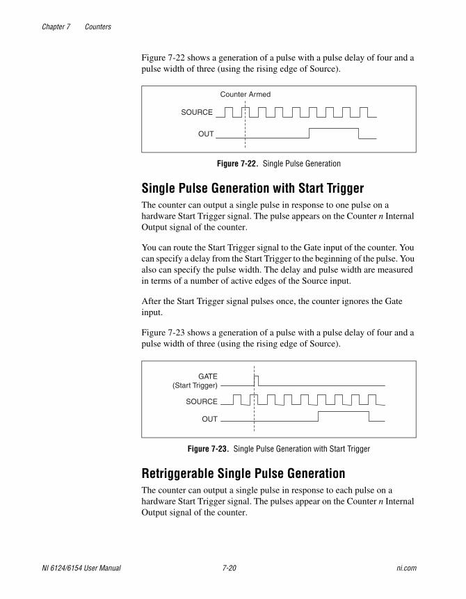
Chapter 7 Counters
NI 6124/6154 User Manual 7-20 ni.com
Figure 7-22 shows a generation of a pulse with a pulse delay of four and a pulse width of three (using the rising edge of Source).
Figure 7-22. Single Pulse Generation
Single Pulse Generation with Start TriggerThe counter can output a single pulse in response to one pulse on a hardware Start Trigger signal. The pulse appears on the Counter n Internal Output signal of the counter.
You can route the Start Trigger signal to the Gate input of the counter. You can specify a delay from the Start Trigger to the beginning of the pulse. You also can specify the pulse width. The delay and pulse width are measured in terms of a number of active edges of the Source input.
After the Start Trigger signal pulses once, the counter ignores the Gate input.
Figure 7-23 shows a generation of a pulse with a pulse delay of four and a pulse width of three (using the rising edge of Source).
Figure 7-23. Single Pulse Generation with Start Trigger
Retriggerable Single Pulse GenerationThe counter can output a single pulse in response to each pulse on a hardware Start Trigger signal. The pulses appear on the Counter n Internal Output signal of the counter.
SOURCE
OUT
Counter Armed
SOURCE
GATE(Start Trigger)
OUT
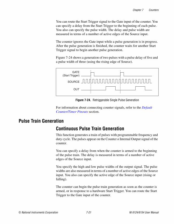
Chapter 7 Counters
© National Instruments Corporation 7-21 NI 6124/6154 User Manual
You can route the Start Trigger signal to the Gate input of the counter. You can specify a delay from the Start Trigger to the beginning of each pulse. You also can specify the pulse width. The delay and pulse width are measured in terms of a number of active edges of the Source input.
The counter ignores the Gate input while a pulse generation is in progress. After the pulse generation is finished, the counter waits for another Start Trigger signal to begin another pulse generation.
Figure 7-24 shows a generation of two pulses with a pulse delay of five and a pulse width of three (using the rising edge of Source).
Figure 7-24. Retriggerable Single Pulse Generation
For information about connecting counter signals, refer to the Default Counter/Timer Pinouts section.
Pulse Train Generation
Continuous Pulse Train GenerationThis function generates a train of pulses with programmable frequency and duty cycle. The pulses appear on the Counter n Internal Output signal of the counter.
You can specify a delay from when the counter is armed to the beginning of the pulse train. The delay is measured in terms of a number of active edges of the Source input.
You specify the high and low pulse widths of the output signal. The pulse widths are also measured in terms of a number of active edges of the Source input. You also can specify the active edge of the Source input (rising or falling).
The counter can begin the pulse train generation as soon as the counter is armed, or in response to a hardware Start Trigger. You can route the Start Trigger to the Gate input of the counter.
SOURCE
GATE(Start Trigger)
OUT
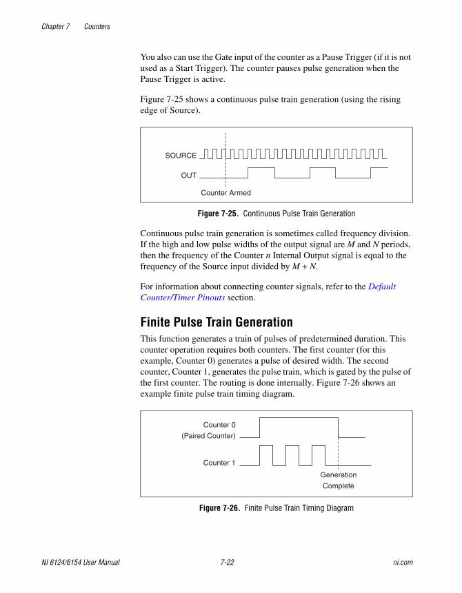
Chapter 7 Counters
NI 6124/6154 User Manual 7-22 ni.com
You also can use the Gate input of the counter as a Pause Trigger (if it is not used as a Start Trigger). The counter pauses pulse generation when the Pause Trigger is active.
Figure 7-25 shows a continuous pulse train generation (using the rising edge of Source).
Figure 7-25. Continuous Pulse Train Generation
Continuous pulse train generation is sometimes called frequency division. If the high and low pulse widths of the output signal are M and N periods, then the frequency of the Counter n Internal Output signal is equal to the frequency of the Source input divided by M + N.
For information about connecting counter signals, refer to the Default Counter/Timer Pinouts section.
Finite Pulse Train GenerationThis function generates a train of pulses of predetermined duration. This counter operation requires both counters. The first counter (for this example, Counter 0) generates a pulse of desired width. The second counter, Counter 1, generates the pulse train, which is gated by the pulse of the first counter. The routing is done internally. Figure 7-26 shows an example finite pulse train timing diagram.
Figure 7-26. Finite Pulse Train Timing Diagram
SOURCE
OUT
Counter Armed
Counter 0
(Paired Counter)
Counter 1
Generation
Complete
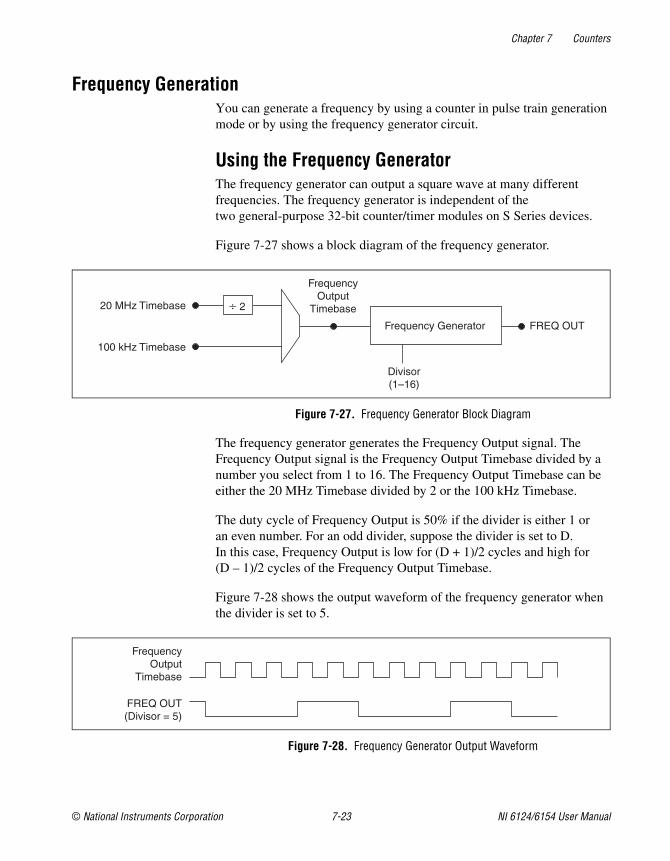
Chapter 7 Counters
© National Instruments Corporation 7-23 NI 6124/6154 User Manual
Frequency GenerationYou can generate a frequency by using a counter in pulse train generation mode or by using the frequency generator circuit.
Using the Frequency GeneratorThe frequency generator can output a square wave at many different frequencies. The frequency generator is independent of the two general-purpose 32-bit counter/timer modules on S Series devices.
Figure 7-27 shows a block diagram of the frequency generator.
Figure 7-27. Frequency Generator Block Diagram
The frequency generator generates the Frequency Output signal. The Frequency Output signal is the Frequency Output Timebase divided by a number you select from 1 to 16. The Frequency Output Timebase can be either the 20 MHz Timebase divided by 2 or the 100 kHz Timebase.
The duty cycle of Frequency Output is 50% if the divider is either 1 or an even number. For an odd divider, suppose the divider is set to D. In this case, Frequency Output is low for (D + 1)/2 cycles and high for (D – 1)/2 cycles of the Frequency Output Timebase.
Figure 7-28 shows the output waveform of the frequency generator when the divider is set to 5.
Figure 7-28. Frequency Generator Output Waveform
100 kHz Timebase
20 MHz Timebase
FrequencyOutput
Timebase
FREQ OUT
Divisor(1–16)
Frequency Generator
÷ 2
FrequencyOutput
Timebase
FREQ OUT(Divisor = 5)
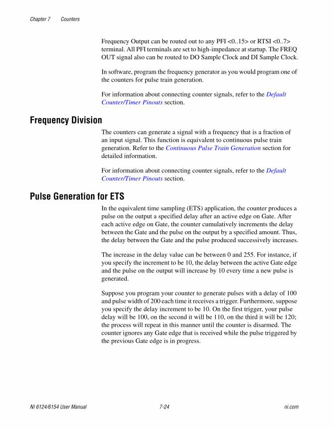
Chapter 7 Counters
NI 6124/6154 User Manual 7-24 ni.com
Frequency Output can be routed out to any PFI <0..15> or RTSI <0..7> terminal. All PFI terminals are set to high-impedance at startup. The FREQ OUT signal also can be routed to DO Sample Clock and DI Sample Clock.
In software, program the frequency generator as you would program one of the counters for pulse train generation.
For information about connecting counter signals, refer to the Default Counter/Timer Pinouts section.
Frequency DivisionThe counters can generate a signal with a frequency that is a fraction of an input signal. This function is equivalent to continuous pulse train generation. Refer to the Continuous Pulse Train Generation section for detailed information.
For information about connecting counter signals, refer to the Default Counter/Timer Pinouts section.
Pulse Generation for ETSIn the equivalent time sampling (ETS) application, the counter produces a pulse on the output a specified delay after an active edge on Gate. After each active edge on Gate, the counter cumulatively increments the delay between the Gate and the pulse on the output by a specified amount. Thus, the delay between the Gate and the pulse produced successively increases.
The increase in the delay value can be between 0 and 255. For instance, if you specify the increment to be 10, the delay between the active Gate edge and the pulse on the output will increase by 10 every time a new pulse is generated.
Suppose you program your counter to generate pulses with a delay of 100 and pulse width of 200 each time it receives a trigger. Furthermore, suppose you specify the delay increment to be 10. On the first trigger, your pulse delay will be 100, on the second it will be 110, on the third it will be 120; the process will repeat in this manner until the counter is disarmed. The counter ignores any Gate edge that is received while the pulse triggered by the previous Gate edge is in progress.
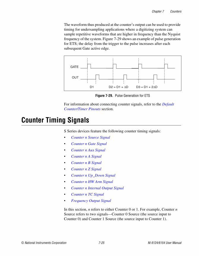
Chapter 7 Counters
© National Instruments Corporation 7-25 NI 6124/6154 User Manual
The waveform thus produced at the counter’s output can be used to provide timing for undersampling applications where a digitizing system can sample repetitive waveforms that are higher in frequency than the Nyquist frequency of the system. Figure 7-29 shows an example of pulse generation for ETS; the delay from the trigger to the pulse increases after each subsequent Gate active edge.
Figure 7-29. Pulse Generation for ETS
For information about connecting counter signals, refer to the Default Counter/Timer Pinouts section.
Counter Timing SignalsS Series devices feature the following counter timing signals:
• Counter n Source Signal
• Counter n Gate Signal
• Counter n Aux Signal
• Counter n A Signal
• Counter n B Signal
• Counter n Z Signal
• Counter n Up_Down Signal
• Counter n HW Arm Signal
• Counter n Internal Output Signal
• Counter n TC Signal
• Frequency Output Signal
In this section, n refers to either Counter 0 or 1. For example, Counter n Source refers to two signals—Counter 0 Source (the source input to Counter 0) and Counter 1 Source (the source input to Counter 1).
OUT
D1 D2 = D1 + ΔD D3 = D1 + 2ΔD
GATE
Chapter 7 Counters
NI 6124/6154 User Manual 7-26 ni.com
Counter n Source SignalThe selected edge of the Counter n Source signal increments and decrements the counter value depending on the application the counter is performing. Table 7-3 lists how this terminal is used in various applications.
Routing a Signal to Counter n SourceEach counter has independent input selectors for the Counter n Source signal. Any of the following signals can be routed to the Counter n Source input:
• 80 MHz Timebase
• 20 MHz Timebase
• 100 kHz Timebase
• RTSI <0..7>
• PFI <0..15>
• PXI_CLK10
• PXI_STAR
• Analog Comparison Event
In addition, Counter 1 TC or Counter 1 Gate can be routed to Counter 0 Source. Counter 0 TC or Counter 0 Gate can be routed to Counter 1 Source.
Some of these options may not be available in some driver software.
Table 7-3. Counter Applications and Counter n Source
Application Purpose of Source Terminal
Pulse Generation Counter Timebase
One Counter Time Measurements Counter Timebase
Two Counter Time Measurements Input Terminal
Non-Buffered Edge Counting Input Terminal
Buffered Edge Counting Input Terminal
Two-Edge Separation Counter Timebase
Chapter 7 Counters
© National Instruments Corporation 7-27 NI 6124/6154 User Manual
Routing Counter n Source to an Output TerminalYou can route Counter n Source out to any PFI <0..15> or RTSI <0..7> terminal. All PFIs are set to high-impedance at startup.
Counter n Gate SignalThe Counter n Gate signal can perform many different operations depending on the application including starting and stopping the counter, and saving the counter contents.
Routing a Signal to Counter n GateEach counter has independent input selectors for the Counter n Gate signal. Any of the following signals can be routed to the Counter n Gate input:
• RTSI <0..7>
• PFI <0..15>
• AI Reference Trigger (ai/ReferenceTrigger)
• AI Start Trigger (ai/StartTrigger)
• AI Sample Clock (ai/SampleClock)
• AI Convert Clock (ai/ConvertClock)
• AO Sample Clock (ao/SampleClock)
• DI Sample Clock (di/SampleClock)
• DO Sample Clock (do/SampleClock)
• PXI_STAR
• Change Detection Event
• Analog Comparison Event
In addition, Counter 1 Internal Output or Counter 1 Source can be routed to Counter 0 Gate. Counter 0 Internal Output or Counter 0 Source can be routed to Counter 1 Gate.
Some of these options may not be available in some driver software.
Routing Counter n Gate to an Output TerminalYou can route Counter n Gate out to any PFI <0..15> or RTSI <0..7> terminal. All PFIs are set to high-impedance at startup.
Chapter 7 Counters
NI 6124/6154 User Manual 7-28 ni.com
Counter n Aux SignalThe Counter n Aux signal indicates the first edge in a two-signal edge-separation measurement.
Routing a Signal to Counter n AuxEach counter has independent input selectors for the Counter n Aux signal. Any of the following signals can be routed to the Counter n Aux input:
• RTSI <0..7>
• PFI <0..15>
• AI Reference Trigger (ai/ReferenceTrigger)
• AI Start Trigger (ai/StartTrigger)
• PXI_STAR
• Analog Comparison Event
In addition, Counter 1 Internal Output, Counter 1 Gate, Counter 1 Source, or Counter 0 Gate can be routed to Counter 0 Aux. Counter 0 Internal Output, Counter 0 Gate, Counter 0 Source, or Counter 1 Gate can be routed to Counter 1 Aux.
Some of these options may not be available in some driver software.
Counter n A, Counter n B, and Counter n Z SignalsCounter n B can control the direction of counting in edge counting applications. Use the A, B, and Z inputs to each counter when measuring quadrature encoders or measuring two pulse encoders.
Routing Signals to A, B, and Z Counter InputsEach counter has independent input selectors for each of the A, B, and Z inputs. Any of the following signals can be routed to each input:
• RTSI <0..7>
• PFI <0..15>
• PXI_STAR
• Analog Comparison Event
Routing Counter n Z Signal to an Output TerminalYou can route Counter n Z out to RTSI <0..7>.
Chapter 7 Counters
© National Instruments Corporation 7-29 NI 6124/6154 User Manual
Counter n Up_Down SignalCounter n Up_Down is another name for the Counter n B signal.
Counter n HW Arm SignalThe Counter n HW Arm signal enables a counter to begin an input or output function.
To begin any counter input or output function, you must first enable, or arm, the counter. In some applications, such as buffered semi-period measurement, the counter begins counting when it is armed. In other applications, such as single pulse-width measurement, the counter begins waiting for the Gate signal when it is armed. Counter output operations can use the arm signal in addition to a start trigger.
Software can arm a counter or configure counters to be armed on a hardware signal. Software calls this hardware signal the Arm Start Trigger. Internally, software routes the Arm Start Trigger to the Counter n HW Arm input of the counter.
Routing Signals to Counter n HW Arm InputAny of the following signals can be routed to the Counter n HW Arm input:
• RTSI <0..7>
• PFI <0..15>
• AI Reference Trigger (ai/ReferenceTrigger)
• AI Start Trigger (ai/StartTrigger)
• PXI_STAR
• Analog Comparison Event
Counter 1 Internal Output can be routed to Counter 0 HW Arm. Counter 0 Internal Output can be routed to Counter 1 HW Arm.
Some of these options may not be available in some driver software.
Counter n Internal Output and Counter n TC SignalsThe Counter n Internal Output signal changes in response to Counter n TC.
The two software-selectable output options are pulse output on TC and toggle output on TC. The output polarity is software-selectable for both options.
Chapter 7 Counters
NI 6124/6154 User Manual 7-30 ni.com
With pulse or pulse train generation tasks, the counter drives the pulse(s) on the Counter n Internal Output signal. The Counter n Internal Output signal can be internally routed to be a counter/timer input or an “external” source for AI, AO, DI, or DO timing signals.
Routing Counter n Internal Output to an Output TerminalYou can route Counter n Internal Output to any PFI <0..15> or RTSI <0..7> terminal. All PFIs are set to high-impedance at startup.
Frequency Output SignalThe Frequency Output (FREQ OUT) signal is the output of the frequency output generator.
Routing Frequency Output to a TerminalYou can route Frequency Output to any PFI <0..15> terminal. All PFIs are set to high-impedance at startup. The FREQ OUT signal also can be routed to DO Sample Clock and DI Sample Clock.
Default Counter/Timer PinoutsBy default, NI-DAQmx routes the counter/timer inputs and outputs to the PFI pins. Refer to Appendix A, Device-Specific Information, for the default counter/timer pin table for your device.
You can use these defaults or select other sources and destinations for the counter/timer signals in NI-DAQmx. Refer to Connecting Counter Signals in the NI-DAQmx Help or the LabVIEW Help in version 8.0 or later for more information about how to connect your signals for common counter measurements and generations. DAQ-STC2-based S Series default PFI lines for counter functions are listed in Physical Channels in the NI-DAQmx Help or the LabVIEW Help in version 8.0 or later.
Chapter 7 Counters
© National Instruments Corporation 7-31 NI 6124/6154 User Manual
Counter TriggeringCounters support three different triggering actions:
• Arm Start Trigger—To begin any counter input or output function, you must first enable, or arm, the counter. Software can arm a counter or configure counters to be armed on a hardware signal. Software calls this hardware signal the Arm Start Trigger. Internally, software routes the Arm Start Trigger to the Counter n HW Arm input of the counter.
For counter output operations, you can use it in addition to the start and pause triggers. For counter input operations, you can use the arm start trigger to have start trigger-like behavior. The arm start trigger can be used for synchronizing multiple counter input and output tasks.
When using an arm start trigger, the arm start trigger source is routed to the Counter n HW Arm signal.
• Start Trigger—For counter output operations, a start trigger can be configured to begin a finite or continuous pulse generation. Once a continuous generation has triggered, the pulses continue to generate until you stop the operation in software. For finite generations, the specified number of pulses is generated and the generation stops unless you use the retriggerable attribute. When you use this attribute, subsequent start triggers cause the generation to restart.
When using a start trigger, the start trigger source is routed to the Counter n Gate signal input of the counter.
Counter input operations can use the arm start trigger to have start trigger-like behavior.
• Pause Trigger—You can use pause triggers in edge counting and continuous pulse generation applications. For edge counting acquisitions, the counter stops counting edges while the external trigger signal is low and resumes when the signal goes high or vice versa. For continuous pulse generations, the counter stops generating pulses while the external trigger signal is low and resumes when the signal goes high or vice versa.
When using a pause trigger, the pause trigger source is routed to the Counter n Gate signal input of the counter.
Chapter 7 Counters
NI 6124/6154 User Manual 7-32 ni.com
Other Counter Features
Cascading CountersYou can internally route the Counter n Internal Output and Counter n TC signals of each counter to the Gate inputs of the other counter. By cascading two counters together, you can effectively create a 64-bit counter. By cascading counters, you also can enable other applications. For example, to improve the accuracy of frequency measurements, use reciprocal frequency measurement, as described in the Method 3 bullet in the Frequency Measurement section.
Counter FiltersYou can enable a programmable debouncing filter on each PFI, RTSI, or PXI_STAR signal. When the filters are enabled, your device samples the input on each rising edge of a filter clock. S Series devices use an onboard oscillator to generate the filter clock with a 40 MHz frequency.
Note NI-DAQmx only supports filters on counter inputs.
The following is an example of low to high transitions of the input signal. High to low transitions work similarly.
Assume that an input terminal has been low for a long time. The input terminal then changes from low to high, but glitches several times. When the filter clock has sampled the signal high on N consecutive edges, the low to high transition is propagated to the rest of the circuit. The value of N depends on the filter setting; refer to Table 7-4.
Table 7-4. Filters
Filter Setting
N (Filter Clocks Needed to
Pass Signal)
Pulse Width Guaranteed to
Pass Filter
Pulse Width Guaranteed to Not Pass Filter
125 ns 5 125 ns 100 ns
6.425 μs 257 6.425 μs 6.400 μs
2.56 ms ~101,800 2.56 ms 2.54 ms
Disabled — — —
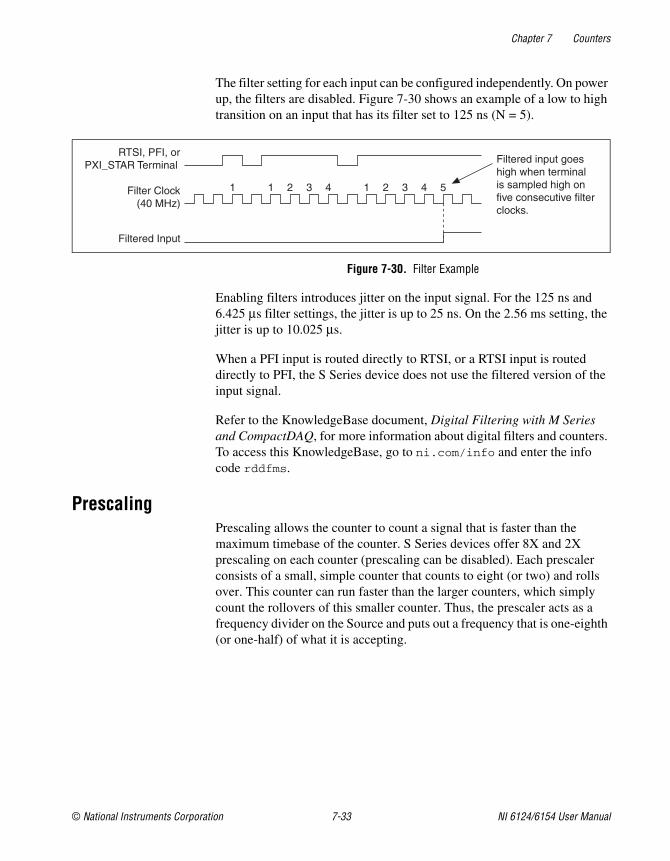
Chapter 7 Counters
© National Instruments Corporation 7-33 NI 6124/6154 User Manual
The filter setting for each input can be configured independently. On power up, the filters are disabled. Figure 7-30 shows an example of a low to high transition on an input that has its filter set to 125 ns (N = 5).
Figure 7-30. Filter Example
Enabling filters introduces jitter on the input signal. For the 125 ns and 6.425 μs filter settings, the jitter is up to 25 ns. On the 2.56 ms setting, the jitter is up to 10.025 μs.
When a PFI input is routed directly to RTSI, or a RTSI input is routed directly to PFI, the S Series device does not use the filtered version of the input signal.
Refer to the KnowledgeBase document, Digital Filtering with M Series and CompactDAQ, for more information about digital filters and counters. To access this KnowledgeBase, go to ni.com/info and enter the info code rddfms.
PrescalingPrescaling allows the counter to count a signal that is faster than the maximum timebase of the counter. S Series devices offer 8X and 2X prescaling on each counter (prescaling can be disabled). Each prescaler consists of a small, simple counter that counts to eight (or two) and rolls over. This counter can run faster than the larger counters, which simply count the rollovers of this smaller counter. Thus, the prescaler acts as a frequency divider on the Source and puts out a frequency that is one-eighth (or one-half) of what it is accepting.
1 2 3 1 4 1 2 3 4 5
RTSI, PFI, or PXI_STAR Terminal
Filter Clock (40 MHz)
Filtered Input
Filtered input goes high when terminal is sampled high on five consecutive filter clocks.
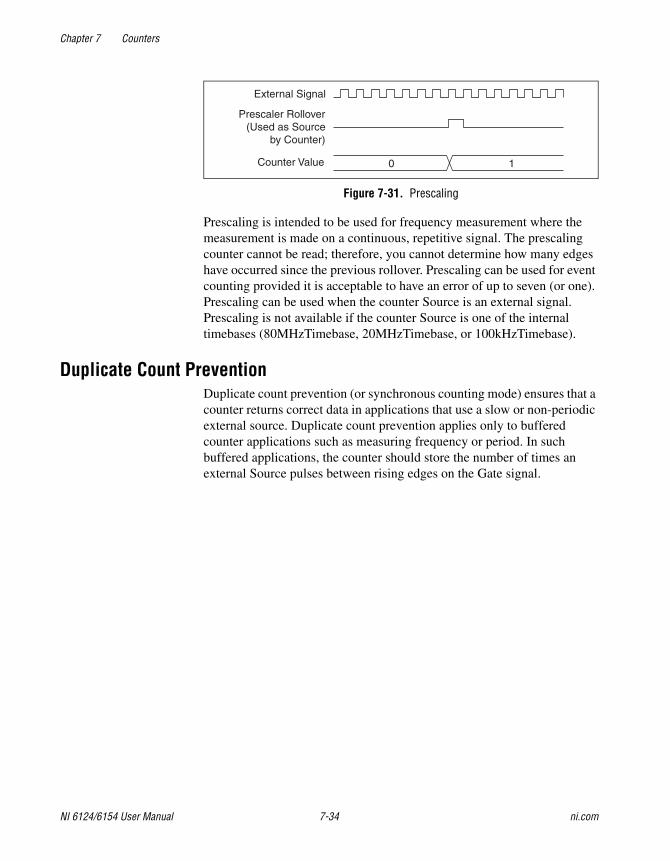
Chapter 7 Counters
NI 6124/6154 User Manual 7-34 ni.com
Figure 7-31. Prescaling
Prescaling is intended to be used for frequency measurement where the measurement is made on a continuous, repetitive signal. The prescaling counter cannot be read; therefore, you cannot determine how many edges have occurred since the previous rollover. Prescaling can be used for event counting provided it is acceptable to have an error of up to seven (or one). Prescaling can be used when the counter Source is an external signal. Prescaling is not available if the counter Source is one of the internal timebases (80MHzTimebase, 20MHzTimebase, or 100kHzTimebase).
Duplicate Count PreventionDuplicate count prevention (or synchronous counting mode) ensures that a counter returns correct data in applications that use a slow or non-periodic external source. Duplicate count prevention applies only to buffered counter applications such as measuring frequency or period. In such buffered applications, the counter should store the number of times an external Source pulses between rising edges on the Gate signal.
External Signal
Counter Value
Prescaler Rollover (Used as Source
by Counter)
0 1
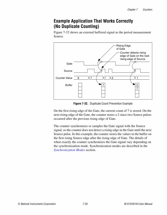
Chapter 7 Counters
© National Instruments Corporation 7-35 NI 6124/6154 User Manual
Example Application That Works Correctly (No Duplicate Counting)Figure 7-32 shows an external buffered signal as the period measurement Source.
Figure 7-32. Duplicate Count Prevention Example
On the first rising edge of the Gate, the current count of 7 is stored. On the next rising edge of the Gate, the counter stores a 2 since two Source pulses occurred after the previous rising edge of Gate.
The counter synchronizes or samples the Gate signal with the Source signal, so the counter does not detect a rising edge in the Gate until the next Source pulse. In this example, the counter stores the values in the buffer on the first rising Source edge after the rising edge of Gate. The details of when exactly the counter synchronizes the Gate signal vary depending on the synchronization mode. Synchronization modes are described in the Synchronization Modes section.
2 7
7
6 7 1 2 1
Rising Edge of Gate
Counter detects rising edge of Gate on the next rising edge of Source.
Source
Gate
Buffer
Counter Value
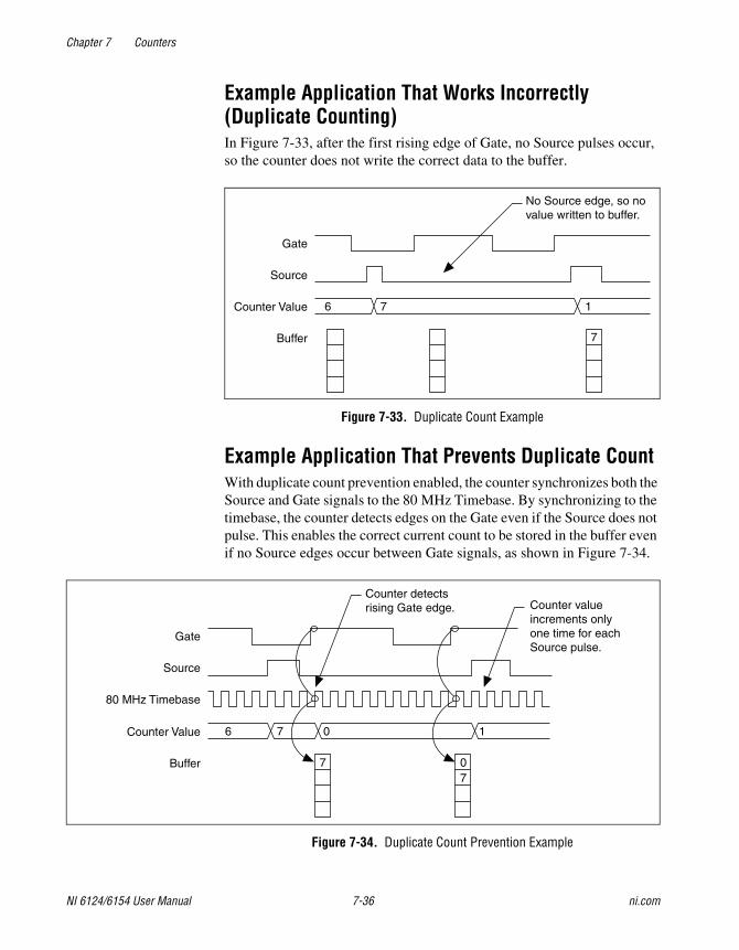
Chapter 7 Counters
NI 6124/6154 User Manual 7-36 ni.com
Example Application That Works Incorrectly (Duplicate Counting)In Figure 7-33, after the first rising edge of Gate, no Source pulses occur, so the counter does not write the correct data to the buffer.
Figure 7-33. Duplicate Count Example
Example Application That Prevents Duplicate CountWith duplicate count prevention enabled, the counter synchronizes both the Source and Gate signals to the 80 MHz Timebase. By synchronizing to the timebase, the counter detects edges on the Gate even if the Source does not pulse. This enables the correct current count to be stored in the buffer even if no Source edges occur between Gate signals, as shown in Figure 7-34.
Figure 7-34. Duplicate Count Prevention Example
7
6 7 1
No Source edge, so novalue written to buffer.
Source
Gate
Buffer
Counter Value
0 7
7
6 7 0 1
Counter detectsrising Gate edge. Counter value
increments onlyone time for eachSource pulse.
Source
80 MHz Timebase
Gate
Buffer
Counter Value
Chapter 7 Counters
© National Instruments Corporation 7-37 NI 6124/6154 User Manual
Even if the Source pulses are long, the counter increments only once for each Source pulse.
Normally, the counter value and Counter n Internal Output signals change synchronously to the Source signal. With duplicate count prevention, the counter value and Counter n Internal Output signals change synchronously to the 80 MHz Timebase.
Note that duplicate count prevention should only be used if the frequency of the Source signal is 20 MHz or less.
When To Use Duplicate Count PreventionYou should use duplicate count prevention if the following conditions are true:
• You are making a counter measurement.
• You are using an external signal (such as PFI x) as the counter Source.
• The frequency of the external source is 20 MHz or less.
• You can have the counter value and output to change synchronously with the 80 MHz Timebase.
In all other cases, you should not use duplicate count prevention.
Enabling Duplicate Count Prevention in NI-DAQmxYou can enable duplicate count prevention in NI-DAQmx by setting the Enable Duplicate Count Prevention attribute/property. For specific information about finding the Enable Duplicate Count Prevention attribute/property, refer to the help file for the API you are using.
Synchronization ModesThe 32-bit counter counts up or down synchronously with the Source signal. The Gate signal and other counter inputs are asynchronous to the Source signal. So S Series devices synchronize these signals before presenting them to the internal counter.
S Series devices use one of three synchronization methods:
• 80 MHz source mode
• Other internal source mode
• External source mode
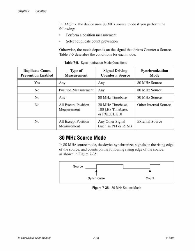
Chapter 7 Counters
NI 6124/6154 User Manual 7-38 ni.com
In DAQmx, the device uses 80 MHz source mode if you perform the following:
• Perform a position measurement
• Select duplicate count prevention
Otherwise, the mode depends on the signal that drives Counter n Source. Table 7-5 describes the conditions for each mode.
80 MHz Source ModeIn 80 MHz source mode, the device synchronizes signals on the rising edge of the source, and counts on the following rising edge of the source, as shown in Figure 7-35.
Figure 7-35. 80 MHz Source Mode
Table 7-5. Synchronization Mode Conditions
Duplicate Count Prevention Enabled
Type of Measurement
Signal Driving Counter n Source
Synchronization Mode
Yes Any Any 80 MHz Source
No Position Measurement Any 80 MHz Source
No Any 80 MHz Timebase 80 MHz Source
No All Except Position Measurement
20 MHz Timebase, 100 kHz Timebase, or PXI_CLK10
Other Internal Source
No All Except Position Measurement
Any Other Signal (such as PFI or RTSI)
External Source
Source
Synchronize Count
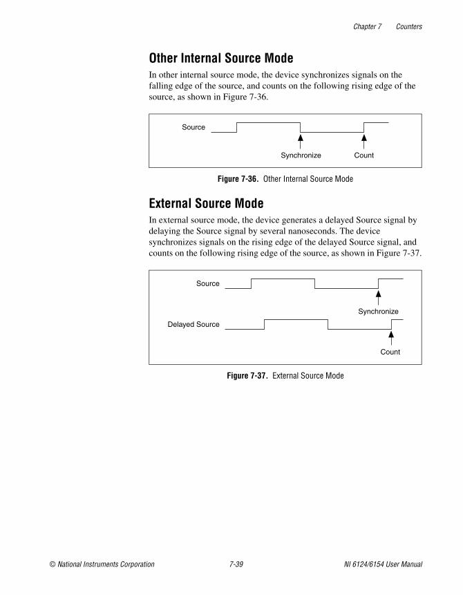
Chapter 7 Counters
© National Instruments Corporation 7-39 NI 6124/6154 User Manual
Other Internal Source ModeIn other internal source mode, the device synchronizes signals on the falling edge of the source, and counts on the following rising edge of the source, as shown in Figure 7-36.
Figure 7-36. Other Internal Source Mode
External Source ModeIn external source mode, the device generates a delayed Source signal by delaying the Source signal by several nanoseconds. The device synchronizes signals on the rising edge of the delayed Source signal, and counts on the following rising edge of the source, as shown in Figure 7-37.
Figure 7-37. External Source Mode
Source
Synchronize Count
Source
Delayed Source
Synchronize
Count
© National Instruments Corporation 8-1 NI 6124/6154 User Manual
8Programmable Function Interfaces (PFI)
Refer to one of the following sections, depending on your device:
• PFI for Non-Isolated Devices—NI 6124 devices have 16 PFI pins in addition to eight lines of bidirectional DIO signals.
• PFI for Isolated Devices—NI 6154 devices have 10 equivalent directional PFI pins that can be independently configured as an input or output.
PFI for Non-Isolated Devices(NI 6124 Only) Non-isolated S Series devices have 16 Programmable Function Interface (PFI) signals. In addition, these devices have eight lines of bidirectional DIO signals.
Each PFI can be individually configured as the following:
• A static digital input
• A static digital output
• A timing input signal for AI, AO, DI, DO, or counter/timer functions
• A timing output signal from AI, AO, DI, DO, or counter/timer functions
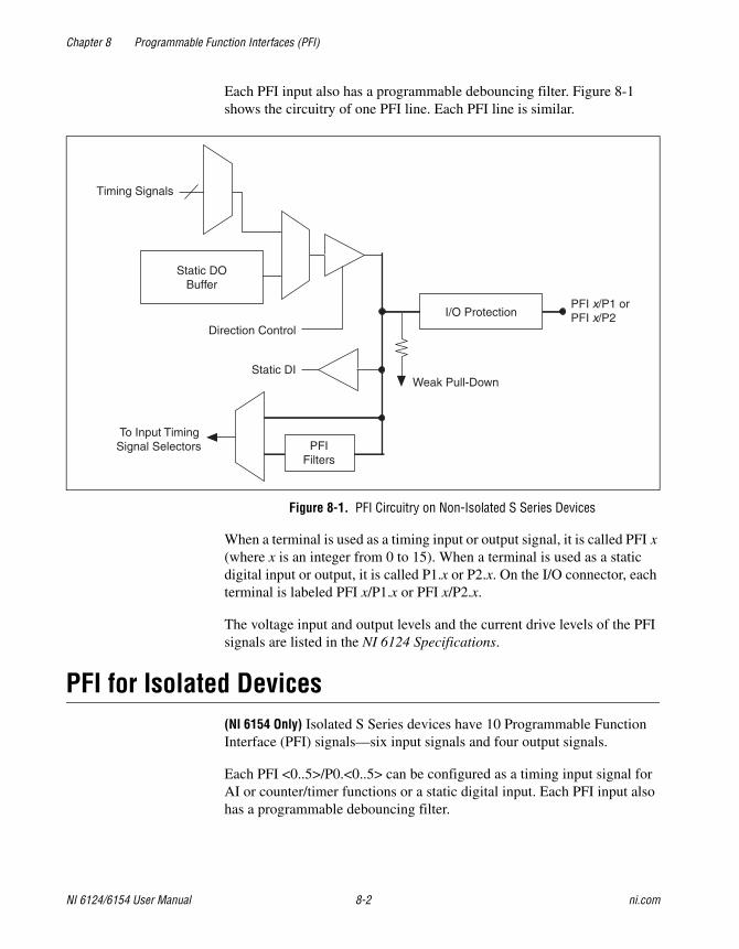
Chapter 8 Programmable Function Interfaces (PFI)
NI 6124/6154 User Manual 8-2 ni.com
Each PFI input also has a programmable debouncing filter. Figure 8-1 shows the circuitry of one PFI line. Each PFI line is similar.
Figure 8-1. PFI Circuitry on Non-Isolated S Series Devices
When a terminal is used as a timing input or output signal, it is called PFI x (where x is an integer from 0 to 15). When a terminal is used as a static digital input or output, it is called P1.x or P2.x. On the I/O connector, each terminal is labeled PFI x/P1.x or PFI x/P2.x.
The voltage input and output levels and the current drive levels of the PFI signals are listed in the NI 6124 Specifications.
PFI for Isolated Devices(NI 6154 Only) Isolated S Series devices have 10 Programmable Function Interface (PFI) signals—six input signals and four output signals.
Each PFI <0..5>/P0.<0..5> can be configured as a timing input signal for AI or counter/timer functions or a static digital input. Each PFI input also has a programmable debouncing filter.
Timing Signals
Direction Control
Static DI
I/O Protection
Weak Pull-Down
PFI x/P1 orPFI x/P2
Static DOBuffer
To Input Timing Signal Selectors PFI
Filters
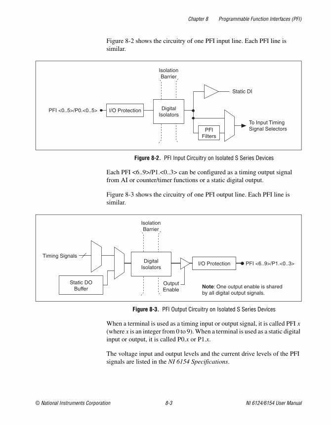
Chapter 8 Programmable Function Interfaces (PFI)
© National Instruments Corporation 8-3 NI 6124/6154 User Manual
Figure 8-2 shows the circuitry of one PFI input line. Each PFI line is similar.
Figure 8-2. PFI Input Circuitry on Isolated S Series Devices
Each PFI <6..9>/P1.<0..3> can be configured as a timing output signal from AI or counter/timer functions or a static digital output.
Figure 8-3 shows the circuitry of one PFI output line. Each PFI line is similar.
Figure 8-3. PFI Output Circuitry on Isolated S Series Devices
When a terminal is used as a timing input or output signal, it is called PFI x (where x is an integer from 0 to 9). When a terminal is used as a static digital input or output, it is called P0.x or P1.x.
The voltage input and output levels and the current drive levels of the PFI signals are listed in the NI 6154 Specifications.
To Input Timing Signal Selectors
Isolation Barrier
Digital Isolators
I/O Protection PFI <0..5>/P0.<0..5>
PFI Filters
Static DI
Timing Signals
I/O Protection PFI <6..9>/P1.<0..3>
OutputEnable
Static DOBuffer
IsolationBarrier
DigitalIsolators
Note: One output enable is shared by all digital output signals.
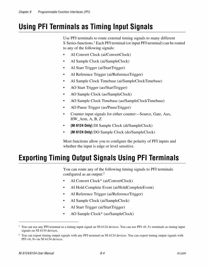
Chapter 8 Programmable Function Interfaces (PFI)
NI 6124/6154 User Manual 8-4 ni.com
Using PFI Terminals as Timing Input SignalsUse PFI terminals to route external timing signals to many different S Series functions.1 Each PFI terminal (or input PFI terminal) can be routed to any of the following signals:
• AI Convert Clock (ai/ConvertClock)
• AI Sample Clock (ai/SampleClock)
• AI Start Trigger (ai/StartTrigger)
• AI Reference Trigger (ai/ReferenceTrigger)
• AI Sample Clock Timebase (ai/SampleClockTimebase)
• AO Start Trigger (ao/StartTrigger)
• AO Sample Clock (ao/SampleClock)
• AO Sample Clock Timebase (ao/SampleClockTimebase)
• AO Pause Trigger (ao/PauseTrigger)
• Counter input signals for either counter—Source, Gate, Aux, HW_Arm, A, B, Z
• (NI 6124 Only) DI Sample Clock (di/SampleClock)
• (NI 6124 Only) DO Sample Clock (do/SampleClock)
Most functions allow you to configure the polarity of PFI inputs and whether the input is edge or level sensitive.
Exporting Timing Output Signals Using PFI TerminalsYou can route any of the following timing signals to PFI terminals configured as an output:2
• AI Convert Clock* (ai/ConvertClock)
• AI Hold Complete Event (ai/HoldCompleteEvent)
• AI Reference Trigger (ai/ReferenceTrigger)
• AI Sample Clock (ai/SampleClock)
• AI Start Trigger (ai/StartTrigger)
• AO Sample Clock* (ao/SampleClock)
1 You can use any PFI terminal as a timing input signal on NI 6124 devices. You can use PFI <0..5> terminals as timing input signals on NI 6154 devices.
2 You can export timing output signals with any PFI terminal on NI 6124 devices. You can export timing output signals with PFI <6..9> on NI 6154 devices.
Chapter 8 Programmable Function Interfaces (PFI)
© National Instruments Corporation 8-5 NI 6124/6154 User Manual
• AO Start Trigger (ao/StartTrigger)
• Counter n Source
• Counter n Gate
• Counter n Internal Output
• Frequency Output
• PXI_STAR
• RTSI <0..7>
• (NI 6124 Only) Analog Comparison Event
• (NI 6124 Only) Change Detection Event
• (NI 6124 Only) DI Sample Clock* (di/SampleClock)
• (NI 6124 Only) DO Sample Clock* (do/SampleClock)
Note Signals with a * are inverted before being driven to a terminal; that is, these signals are active low.
Using PFI Terminals as Static Digital Inputs and OutputsYou can configure PFI terminals to be static digital input or output terminals:
• NI 6124 Devices—Each PFI can be individually configured as a static digital input or a static digital output. When a terminal is used as a static digital input or output, it is called P1.x or P2.x. On the I/O connector, each terminal is labeled PFI x/P1.x or PFI x/P2.x.
In addition, NI 6124 devices have eight lines of bidirectional DIO signals.
• NI 6154 Devices— When a terminal is used as a static digital input or output, it is called P0.x or P1.x. On the I/O connector, each terminal is labeled PFI x/P0.x or PFI x/P1.x.
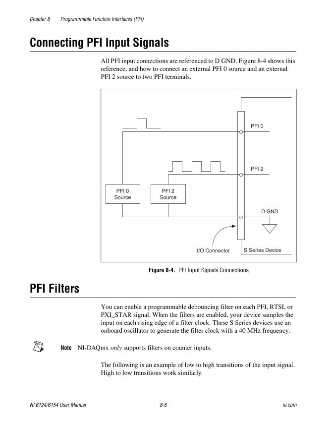
Chapter 8 Programmable Function Interfaces (PFI)
NI 6124/6154 User Manual 8-6 ni.com
Connecting PFI Input SignalsAll PFI input connections are referenced to D GND. Figure 8-4 shows this reference, and how to connect an external PFI 0 source and an external PFI 2 source to two PFI terminals.
Figure 8-4. PFI Input Signals Connections
PFI FiltersYou can enable a programmable debouncing filter on each PFI, RTSI, or PXI_STAR signal. When the filters are enabled, your device samples the input on each rising edge of a filter clock. These S Series devices use an onboard oscillator to generate the filter clock with a 40 MHz frequency.
Note NI-DAQmx only supports filters on counter inputs.
The following is an example of low to high transitions of the input signal. High to low transitions work similarly.
PFI 0Source
PFI 2Source
S Series Device
D GND
PFI 2
PFI 0
I/O Connector
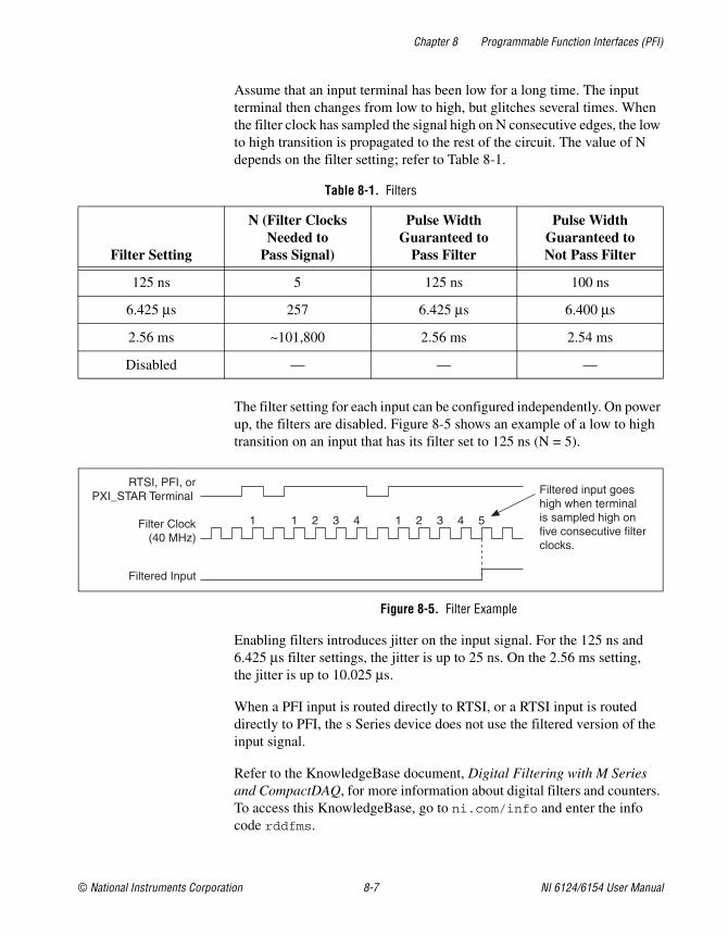
Chapter 8 Programmable Function Interfaces (PFI)
© National Instruments Corporation 8-7 NI 6124/6154 User Manual
Assume that an input terminal has been low for a long time. The input terminal then changes from low to high, but glitches several times. When the filter clock has sampled the signal high on N consecutive edges, the low to high transition is propagated to the rest of the circuit. The value of N depends on the filter setting; refer to Table 8-1.
The filter setting for each input can be configured independently. On power up, the filters are disabled. Figure 8-5 shows an example of a low to high transition on an input that has its filter set to 125 ns (N = 5).
Figure 8-5. Filter Example
Enabling filters introduces jitter on the input signal. For the 125 ns and 6.425 μs filter settings, the jitter is up to 25 ns. On the 2.56 ms setting, the jitter is up to 10.025 μs.
When a PFI input is routed directly to RTSI, or a RTSI input is routed directly to PFI, the s Series device does not use the filtered version of the input signal.
Refer to the KnowledgeBase document, Digital Filtering with M Series and CompactDAQ, for more information about digital filters and counters. To access this KnowledgeBase, go to ni.com/info and enter the info code rddfms.
Table 8-1. Filters
Filter Setting
N (Filter Clocks Needed to
Pass Signal)
Pulse Width Guaranteed to
Pass Filter
Pulse Width Guaranteed to Not Pass Filter
125 ns 5 125 ns 100 ns
6.425 μs 257 6.425 μs 6.400 μs
2.56 ms ~101,800 2.56 ms 2.54 ms
Disabled — — —
1 2 3 1 4 1 2 3 4 5
RTSI, PFI, or PXI_STAR Terminal
Filter Clock (40 MHz)
Filtered Input
Filtered input goes high when terminal is sampled high on five consecutive filter clocks.
Chapter 8 Programmable Function Interfaces (PFI)
NI 6124/6154 User Manual 8-8 ni.com
I/O ProtectionEach DIO and PFI signal is protected against overvoltage, undervoltage, and overcurrent conditions as well as ESD events. However, you should avoid these fault conditions by following these guidelines:
• If you configure a PFI or DIO line as an output, do not connect it to any external signal source, ground, or power supply.
• If you configure a PFI or DIO line as an output, understand the current requirements of the load connected to these signals. Do not exceed the specified current output limits of the DAQ device. NI has several signal conditioning solutions for digital applications requiring high current drive.
• If you configure a PFI or DIO line as an input, do not drive the line with voltages outside of its normal operating range. The PFI or DIO lines have a smaller operating range than the AI signals.
• Treat the DAQ device as you would treat any static sensitive device. Always properly ground yourself and the equipment when handling the DAQ device or connecting to it.
Programmable Power-Up StatesThe programmable power-up state for the DAQ-STC2-based S Series devices are as follows:
• NI 6124 Devices— At system startup and reset, the hardware sets all PFI and DIO lines to high-impedance inputs by default. The DAQ device does not drive the signal high or low. Each line has a weak pull-down resistor connected to it, as described in the specifications document for your device.
NI-DAQmx supports programmable power-up states for PFI and DIO lines. Software can program any value at power up to the P0, P1, or P2 lines. The PFI and DIO lines can be set as:
– A high-impedance input with a weak pull-down resistor (default)
– An output driving a 0
– An output driving a 1
Note When using your S Series device to control an SCXI chassis, DIO lines 0, 1, 2, and 4 are used as communication lines and must be left to power-up in the default high-impedance state to avoid potential damage to these signals.
Chapter 8 Programmable Function Interfaces (PFI)
© National Instruments Corporation 8-9 NI 6124/6154 User Manual
• NI 6154 Devices—By default, the digital output lines (P1.<0..3>/PFI <6..9>) are disabled (high impedance) at power up. Software can configure the board to power up with the entire port enabled or disabled; you cannot enable individual lines. If the port powers up enabled, you also can configure each line individually to power up as 1 or 0.
Refer to the NI-DAQmx Help or the LabVIEW Help in version 8.0 or later for more information about setting power-up states in NI-DAQmx or MAX.
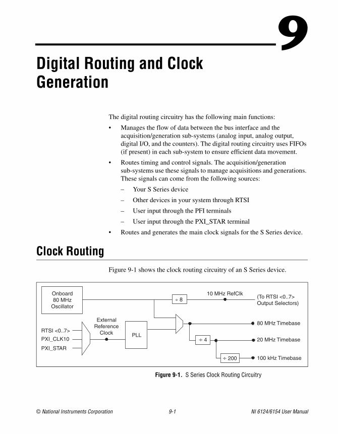
© National Instruments Corporation 9-1 NI 6124/6154 User Manual
9Digital Routing and Clock Generation
The digital routing circuitry has the following main functions:
• Manages the flow of data between the bus interface and the acquisition/generation sub-systems (analog input, analog output, digital I/O, and the counters). The digital routing circuitry uses FIFOs (if present) in each sub-system to ensure efficient data movement.
• Routes timing and control signals. The acquisition/generation sub-systems use these signals to manage acquisitions and generations. These signals can come from the following sources:
– Your S Series device
– Other devices in your system through RTSI
– User input through the PFI terminals
– User input through the PXI_STAR terminal
• Routes and generates the main clock signals for the S Series device.
Clock RoutingFigure 9-1 shows the clock routing circuitry of an S Series device.
Figure 9-1. S Series Clock Routing Circuitry
RTSI <0..7>
Onboard 80 MHz
Oscillator
External Reference
Clock
(To RTSI <0..7> Output Selectors)
10 MHz RefClk
PLL ÷ 4
÷ 200
÷ 8
PXI_CLK10
PXI_STAR
80 MHz Timebase
100 kHz Timebase
20 MHz Timebase
Chapter 9 Digital Routing and Clock Generation
NI 6124/6154 User Manual 9-2 ni.com
80 MHz TimebaseThe 80 MHz Timebase can be used as the Source input to the 32-bit general-purpose counter/timers.
The 80 MHz Timebase is generated from the following sources:
• Onboard oscillator
• External signal (by using the external reference clock)
20 MHz TimebaseThe 20 MHz Timebase normally generates many of the AI and AO timing signals. The 20 MHz Timebase also can be used as the Source input to the 32-bit general-purpose counter/timers.
The 20 MHz Timebase is generated by dividing down the 80 MHz Timebase.
100 kHz TimebaseThe 100 kHz Timebase can be used to generate many of the AI and AO timing signals. The 100 kHz Timebase also can be used as the Source input to the 32-bit general-purpose counter/timers.
The 100 kHz Timebase is generated by dividing down the 20 MHz Timebase by 200.
External Reference ClockThe external reference clock can be used as a source for the internal timebases (80 MHz Timebase, 20 MHz Timebase, and 100 kHz Timebase) on an S Series device. By using the external reference clock, you can synchronize the internal timebases to an external clock.
The following signals can be routed to drive the external reference clock:
• RTSI <0..7>
• PXI_CLK10
• PXI_STAR
The external reference clock is an input to a Phase-Lock Loop (PLL). The PLL generates the internal timebases.
Chapter 9 Digital Routing and Clock Generation
© National Instruments Corporation 9-3 NI 6124/6154 User Manual
10 MHz Reference ClockThe 10 MHz reference clock can be used to synchronize other devices to your S Series device. The 10 MHz reference clock can be routed to the RTSI <0..7> terminals. Other devices connected to the RTSI bus can use this signal as a clock input.
The 10 MHz reference clock is generated by dividing down the onboard oscillator.
Synchronizing Multiple DevicesWith the RTSI bus and the routing capabilities of S Series devices, there are several ways to synchronize multiple devices depending on your application.
To synchronize multiple devices to a common timebase, choose one device—the initiator—to generate the timebase. The initiator device routes its 10 MHz reference clock to one of the RTSI <0..7> signals.
All devices (including the initiator device) receive the 10 MHz reference clock from RTSI. This signal becomes the external reference clock. A PLL on each device generates the internal timebases synchronous to the external reference clock.
On PXI systems, you also can synchronize devices to PXI_CLK10. In this application the PXI chassis acts as the initiator. Each PXI module routes PXI_CLK10 to its external reference clock.
Another option in PXI systems is to use PXI_STAR. The Star Trigger controller device acts as the initiator and drives PXI_STAR with a clock signal. Each target device routes PXI_STAR to its external reference clock.
Once all of the devices are using or referencing a common timebase, you can synchronize operations across them by sending a common start trigger out across the RTSI bus and setting their sample clock rates to the same value.
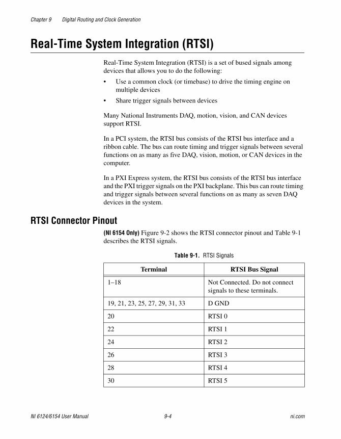
Chapter 9 Digital Routing and Clock Generation
NI 6124/6154 User Manual 9-4 ni.com
Real-Time System Integration (RTSI)Real-Time System Integration (RTSI) is a set of bused signals among devices that allows you to do the following:
• Use a common clock (or timebase) to drive the timing engine on multiple devices
• Share trigger signals between devices
Many National Instruments DAQ, motion, vision, and CAN devices support RTSI.
In a PCI system, the RTSI bus consists of the RTSI bus interface and a ribbon cable. The bus can route timing and trigger signals between several functions on as many as five DAQ, vision, motion, or CAN devices in the computer.
In a PXI Express system, the RTSI bus consists of the RTSI bus interface and the PXI trigger signals on the PXI backplane. This bus can route timing and trigger signals between several functions on as many as seven DAQ devices in the system.
RTSI Connector Pinout(NI 6154 Only) Figure 9-2 shows the RTSI connector pinout and Table 9-1 describes the RTSI signals.
Table 9-1. RTSI Signals
Terminal RTSI Bus Signal
1–18 Not Connected. Do not connect signals to these terminals.
19, 21, 23, 25, 27, 29, 31, 33 D GND
20 RTSI 0
22 RTSI 1
24 RTSI 2
26 RTSI 3
28 RTSI 4
30 RTSI 5
Chapter 9 Digital Routing and Clock Generation
© National Instruments Corporation 9-5 NI 6124/6154 User Manual
Figure 9-2. S Series PCI Device RTSI Pinout
Using RTSI as OutputsRTSI <0..7> are bidirectional terminals. As an output, you can drive any of the following signals to any RTSI terminal:
• AI Start Trigger (ai/StartTrigger)
• AI Reference Trigger (ai/ReferenceTrigger)
• AI Convert Clock* (ai/ConvertClock)
• AI Sample Clock (ai/SampleClock)
• AO Sample Clock* (ao/SampleClock)
• AO Start Trigger (ao/StartTrigger)
• AO Pause Trigger (ao/PauseTrigger)
• 10 MHz Reference Clock
32 RTSI 6
34 RTSI 7
Table 9-1. RTSI Signals (Continued)
Terminal RTSI Bus Signal
Terminal 2
Terminal 34
Terminal 33
Terminal 1
Chapter 9 Digital Routing and Clock Generation
NI 6124/6154 User Manual 9-6 ni.com
• Counter n Source, Gate, Z, Internal Output
• Change Detection Event
• Analog Comparison Event
• FREQ OUT
• PFI <0..5>
Note Signals with a * are inverted before being driven on the RTSI terminals.
Using RTSI Terminals as Timing Input SignalsYou can use RTSI terminals to route external timing signals to many different S Series functions. Each RTSI terminal can be routed to any of the following signals:
• AI Convert Clock (ai/ConvertClock)
• AI Sample Clock (ai/SampleClock)
• AI Start Trigger (ai/StartTrigger)
• AI Reference Trigger (ai/ReferenceTrigger)
• AI Sample Clock Timebase (ai/SampleClockTimebase)
• AO Start Trigger (ao/StartTrigger)
• AO Sample Clock (ao/SampleClock)
• AO Sample Clock Timebase (ao/SampleClockTimebase)
• AO Pause Trigger (ao/PauseTrigger)
• Counter input signals for either counter—Source, Gate, Aux, HW_Arm, A, B, or Z
• DI Sample Clock (di/SampleClock)
• DO Sample Clock (do/SampleClock)
Most functions allow you to configure the polarity of PFI inputs and whether the input is edge or level sensitive.
RTSI FiltersYou can enable a programmable debouncing filter on each PFI, RTSI, or PXI_STAR signal. When the filters are enabled, your device samples the input on each rising edge of a filter clock. S Series devices use an onboard oscillator to generate the filter clock with a 40 MHz frequency.
Note NI-DAQmx only supports filters on counter inputs.
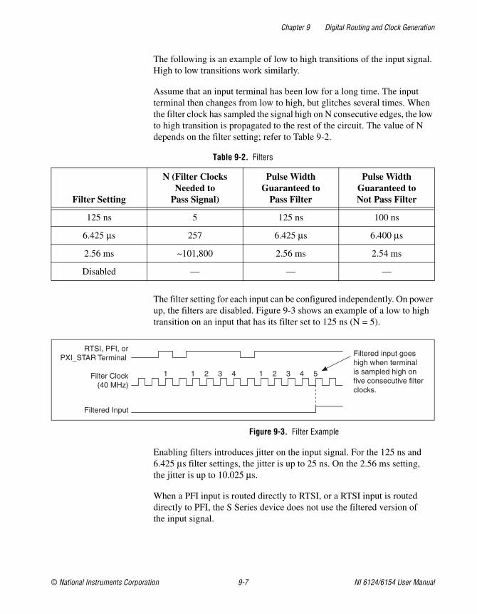
Chapter 9 Digital Routing and Clock Generation
© National Instruments Corporation 9-7 NI 6124/6154 User Manual
The following is an example of low to high transitions of the input signal. High to low transitions work similarly.
Assume that an input terminal has been low for a long time. The input terminal then changes from low to high, but glitches several times. When the filter clock has sampled the signal high on N consecutive edges, the low to high transition is propagated to the rest of the circuit. The value of N depends on the filter setting; refer to Table 9-2.
The filter setting for each input can be configured independently. On power up, the filters are disabled. Figure 9-3 shows an example of a low to high transition on an input that has its filter set to 125 ns (N = 5).
Figure 9-3. Filter Example
Enabling filters introduces jitter on the input signal. For the 125 ns and 6.425 μs filter settings, the jitter is up to 25 ns. On the 2.56 ms setting, the jitter is up to 10.025 μs.
When a PFI input is routed directly to RTSI, or a RTSI input is routed directly to PFI, the S Series device does not use the filtered version of the input signal.
Table 9-2. Filters
Filter Setting
N (Filter Clocks Needed to
Pass Signal)
Pulse Width Guaranteed to
Pass Filter
Pulse Width Guaranteed to Not Pass Filter
125 ns 5 125 ns 100 ns
6.425 μs 257 6.425 μs 6.400 μs
2.56 ms ~101,800 2.56 ms 2.54 ms
Disabled — — —
1 2 3 1 4 1 2 3 4 5
RTSI, PFI, or PXI_STAR Terminal
Filter Clock (40 MHz)
Filtered Input
Filtered input goes high when terminal is sampled high on five consecutive filter clocks.
Chapter 9 Digital Routing and Clock Generation
NI 6124/6154 User Manual 9-8 ni.com
Refer to the KnowledgeBase document, Digital Filtering with M Series and CompactDAQ, for more information about digital filters and counters. To access this KnowledgeBase, go to ni.com/info and enter the info code rddfms.
PXI Clock and Trigger Signals(NI 6124 Only) PXI clock and trigger signals are only available on PXI and PXI Express devices.
PXI_CLK10(NI 6124 Only) PXI_CLK10 is a common low-skew 10 MHz reference clock for synchronization of multiple modules in a PXI measurement or control system. The PXI backplane is responsible for generating PXI_CLK10 independently to each peripheral slot in a PXI chassis.
PXI Triggers(NI 6124 Only) A PXI chassis provides eight bused trigger lines to each module in a system. Triggers may be passed from one module to another, allowing precisely timed responses to asynchronous external events that are being monitored or controlled. Triggers can be used to synchronize the operation of several different PXI peripheral modules.
On S Series devices, the eight PXI trigger signals are synonymous with RTSI <0..7>.
Note that in a PXI chassis with more than eight slots, the PXI trigger lines may be divided into multiple independent buses. Refer to the documentation for your chassis for details.
PXI_STAR Trigger(NI 6124 Only) In a PXI system, the Star Trigger bus implements a dedicated trigger line between the first peripheral slot (adjacent to the system slot) and the other peripheral slots. The Star Trigger can be used to synchronize multiple devices or to share a common trigger signal among devices.
A Star Trigger controller can be installed in this first peripheral slot to provide trigger signals to other peripheral modules. Systems that do not require this functionality can install any standard peripheral module in this first peripheral slot.
Chapter 9 Digital Routing and Clock Generation
© National Instruments Corporation 9-9 NI 6124/6154 User Manual
An S Series device receives the Star Trigger signal (PXI_STAR) from a Star Trigger controller. PXI_STAR can be used as an external source for many AI, AO, and counter signals.
An S Series device is not a Star Trigger controller. An S Series device may be used in the first peripheral slot of a PXI system, but the system will not be able to use the Star Trigger feature.
PXI_STAR Filters(NI 6124 Only) You can enable a programmable debouncing filter on each PFI, RTSI, or PXI_STAR signal. When the filters are enabled, your device samples the input on each rising edge of a filter clock. S Series devices use an onboard oscillator to generate the filter clock with a 40 MHz frequency.
Note NI-DAQmx only supports filters on counter inputs.
The following is an example of low to high transitions of the input signal. High to low transitions work similarly.
Assume that an input terminal has been low for a long time. The input terminal then changes from low to high, but glitches several times. When the filter clock has sampled the signal high on N consecutive edges, the low to high transition is propagated to the rest of the circuit. The value of N depends on the filter setting; refer to Table 9-3.
Table 9-3. Filters
Filter Setting
N (Filter Clocks Needed to
Pass Signal)
Pulse Width Guaranteed to
Pass Filter
Pulse Width Guaranteed to Not Pass Filter
125 ns 5 125 ns 100 ns
6.425 μs 257 6.425 μs 6.400 μs
2.56 ms ~101,800 2.56 ms 2.54 ms
Disabled — — —
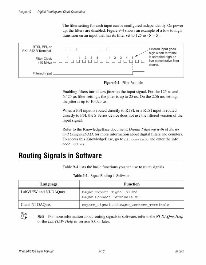
Chapter 9 Digital Routing and Clock Generation
NI 6124/6154 User Manual 9-10 ni.com
The filter setting for each input can be configured independently. On power up, the filters are disabled. Figure 9-4 shows an example of a low to high transition on an input that has its filter set to 125 ns (N = 5).
Figure 9-4. Filter Example
Enabling filters introduces jitter on the input signal. For the 125 ns and 6.425 μs filter settings, the jitter is up to 25 ns. On the 2.56 ms setting, the jitter is up to 10.025 μs.
When a PFI input is routed directly to RTSI, or a RTSI input is routed directly to PFI, the S Series device does not use the filtered version of the input signal.
Refer to the KnowledgeBase document, Digital Filtering with M Series and CompactDAQ, for more information about digital filters and counters. To access this KnowledgeBase, go to ni.com/info and enter the info code rddfms.
Routing Signals in SoftwareTable 9-4 lists the basic functions you can use to route signals.
Note For more information about routing signals in software, refer to the NI-DAQmx Help or the LabVIEW Help in version 8.0 or later.
Table 9-4. Signal Routing in Software
Language Function
LabVIEW and NI-DAQmx DAQmx Export Signal.vi and DAQmx Connect Terminals.vi
C and NI-DAQmx Export_Signal and DAQmx_Connect_Terminals
1 2 3 1 4 1 2 3 4 5
RTSI, PFI, or PXI_STAR Terminal
Filter Clock (40 MHz)
Filtered Input
Filtered input goes high when terminal is sampled high on five consecutive filter clocks.
© National Instruments Corporation 10-1 NI 6124/6154 User Manual
10Bus Interface
Each S Series device is designed on a complete hardware architecture that is deployed on the following platforms:
• PCI
• PXI Express
Using NI-DAQmx driver software, you have the flexibility to change hardware platforms and operating systems with little or no change to software code.
MITE and DAQ-PnPAll S Series devices are jumperless for complete plug-and-play operation. The operating system automatically assigns the base address, interrupt levels, and other resources.
NI S Series PCI/PXIe devices incorporate PCI-MITE technology to implement a high-performance PCI interface.
PXI Considerations(NI 6124 Only) PXI clock and trigger signals are only available on PXI and PXI Express devices.
PXI Clock and Trigger Signals(NI 6124 Only) Refer to the PXI_CLK10, PXI Triggers, PXI_STAR Trigger, and PXI_STAR Filters sections of Chapter 9, Digital Routing and Clock Generation, for more information about PXI clock and trigger signals.
PXI Express(NI 6124 Only) NI PXI Express S Series devices can be installed in any PXI Express slot or PXI hybrid slots in PXI Express chassis. PXI specifications are developed by the PXI System Alliance (www.pxisa.org).
Chapter 10 Bus Interface
NI 6124/6154 User Manual 10-2 ni.com
Data Transfer MethodsThere are three primary ways to transfer data across the PCI bus are as follows:
• Direct Memory Access (DMA)—DMA is a method to transfer data between the device and computer memory without the involvement of the CPU. This method makes DMA the fastest available data transfer method. National Instruments uses DMA hardware and software technology to achieve high throughput rates and to increase system utilization. DMA is the default method of data transfer for DAQ devices that support it.
• Interrupt Request (IRQ)—IRQ transfers rely on the CPU to service data transfer requests. The device notifies the CPU when it is ready to transfer data. The data transfer speed is tightly coupled to the rate at which the CPU can service the interrupt requests. If you are using interrupts to acquire data at a rate faster than the rate the CPU can service the interrupts, your systems may start to freeze.
• Programmed I/O—Programmed I/O is a data transfer mechanism where the user’s program is responsible for transferring data. Each read or write call in the program initiates the transfer of data. Programmed I/O is typically used in software-timed (on demand) operations.
Changing Data Transfer Methods between DMA and IRQThere are a limited number of DMA channels per device (refer to the specifications document for your device). Each operation (specifically, AI, AO, and so on) that requires a DMA channel uses that method until all of the DMA channels are used. After all of the DMA channels are used, you will get an error if you try to run another operation requesting a DMA channel. If appropriate, you can change one of the operations to use interrupts. For NI-DAQmx, use the Data Transfer Mechanism property node.
© National Instruments Corporation 11-1 NI 6124/6154 User Manual
11Triggering
A trigger is a signal that causes a device to perform an action, such as starting an acquisition. You can program your DAQ device to generate triggers on any of the following:
• A software command
• A condition on an external digital signal
• A condition on an external analog signal
You can also program your DAQ device to perform an action in response to a trigger. The action can affect the following:
• Analog input acquisitions
• Analog output generation
• Counter behavior
For more information about analog input triggering, refer to Chapter 4, Analog Input. For more information about analog output triggering, refer to Chapter 5, Analog Output. For more information about counter triggering, refer to Chapter 7, Counters.
Note (NI 6154 Only) NI 6154 devices do not support analog triggering. For information about the triggering capabilities of your device, refer to the specifications document for your device.
Triggering with a Digital SourceYour DAQ device can generate a trigger on a digital signal. You must specify a source and an edge. The digital source can be any of the input PFIs or RTSI <0..6> signals.
The edge can be either the rising edge or falling edge of the digital signal. A rising edge is a transition from a low logic level to a high logic level. A falling edge is a high to low transition.
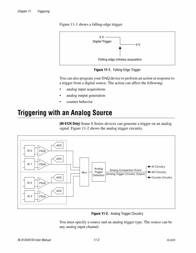
Chapter 11 Triggering
NI 6124/6154 User Manual 11-2 ni.com
Figure 11-1 shows a falling-edge trigger.
Figure 11-1. Falling-Edge Trigger
You can also program your DAQ device to perform an action in response to a trigger from a digital source. The action can affect the following:
• analog input acquisitions
• analog output generation
• counter behavior
Triggering with an Analog Source(NI 6124 Only) Some S Series devices can generate a trigger on an analog signal. Figure 11-2 shows the analog trigger circuitry.
Figure 11-2. Analog Trigger Circuitry
You must specify a source and an analog trigger type. The source can be any analog input channel.
5 V
0 V
Falling edge initiates acquisition
Digital Trigger
AnalogTrigger
DetectionMux
ADC
ADC
Analog Comparison Event(Analog Trigger Circuitry Output)
AO Circuitry
AI Circuitry
Counter CircuitryADC
ADC
PGIAAI 0+
–
PGIAAI 1+
–
PGIAAI 2+
–
PGIAAI 3+
–
Chapter 11 Triggering
© National Instruments Corporation 11-3 NI 6124/6154 User Manual
Analog Input Channel(NI 6124 Only) You can select any analog input channel to drive the instrumentation amplifier. The instrumentation amplifier amplifies the signal as determined by the input mode and the input polarity and range. The output of the instrumentation amplifier then drives the analog trigger detection circuit. By using the instrumentation amplifier, you can trigger on very small voltage changes in the input signal. For more information, refer to the Analog Trigger Accuracy section.
Analog Trigger Actions(NI 6124 Only) The output of the Analog Trigger Detection circuit is the Analog Comparison Event signal. You can program your DAQ device to perform an action in response to the Analog Comparison Event signal. The action can affect the following:
• Analog input acquisitions
• Analog output generation
• Counter behavior
Note Refer to Timing and Triggering in the NI-DAQmx Help or the LabVIEW Help in version 8.0 or later for more information.
Note (NI 6154 Only) The NI 6154 does not support hardware analog triggering.
Analog Trigger Types(NI 6124 Only) Configure the analog trigger circuitry to different triggering modes:
• Analog Edge Triggering—Configure the analog trigger circuitry to detect when the analog signal is below or above a level you specify.
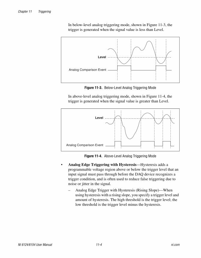
Chapter 11 Triggering
NI 6124/6154 User Manual 11-4 ni.com
In below-level analog triggering mode, shown in Figure 11-3, the trigger is generated when the signal value is less than Level.
Figure 11-3. Below-Level Analog Triggering Mode
In above-level analog triggering mode, shown in Figure 11-4, the trigger is generated when the signal value is greater than Level.
Figure 11-4. Above-Level Analog Triggering Mode
• Analog Edge Triggering with Hysteresis—Hysteresis adds a programmable voltage region above or below the trigger level that an input signal must pass through before the DAQ device recognizes a trigger condition, and is often used to reduce false triggering due to noise or jitter in the signal.
– Analog Edge Trigger with Hysteresis (Rising Slope)—When using hysteresis with a rising slope, you specify a trigger level and amount of hysteresis. The high threshold is the trigger level; the low threshold is the trigger level minus the hysteresis.
Level
Analog Comparison Event
Level
Analog Comparison Event
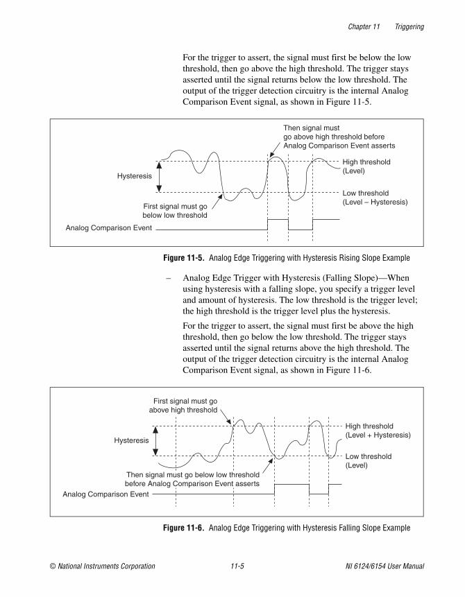
Chapter 11 Triggering
© National Instruments Corporation 11-5 NI 6124/6154 User Manual
For the trigger to assert, the signal must first be below the low threshold, then go above the high threshold. The trigger stays asserted until the signal returns below the low threshold. The output of the trigger detection circuitry is the internal Analog Comparison Event signal, as shown in Figure 11-5.
Figure 11-5. Analog Edge Triggering with Hysteresis Rising Slope Example
– Analog Edge Trigger with Hysteresis (Falling Slope)—When using hysteresis with a falling slope, you specify a trigger level and amount of hysteresis. The low threshold is the trigger level; the high threshold is the trigger level plus the hysteresis.
For the trigger to assert, the signal must first be above the high threshold, then go below the low threshold. The trigger stays asserted until the signal returns above the high threshold. The output of the trigger detection circuitry is the internal Analog Comparison Event signal, as shown in Figure 11-6.
Figure 11-6. Analog Edge Triggering with Hysteresis Falling Slope Example
Analog Comparison Event
Hysteresis
High threshold(Level)
Low threshold(Level – Hysteresis)
First signal must gobelow low threshold
Then signal must go above high threshold before Analog Comparison Event asserts
Analog Comparison Event
Hysteresis
High threshold(Level + Hysteresis)
Low threshold(Level)
First signal must goabove high threshold
Then signal must go below low thresholdbefore Analog Comparison Event asserts
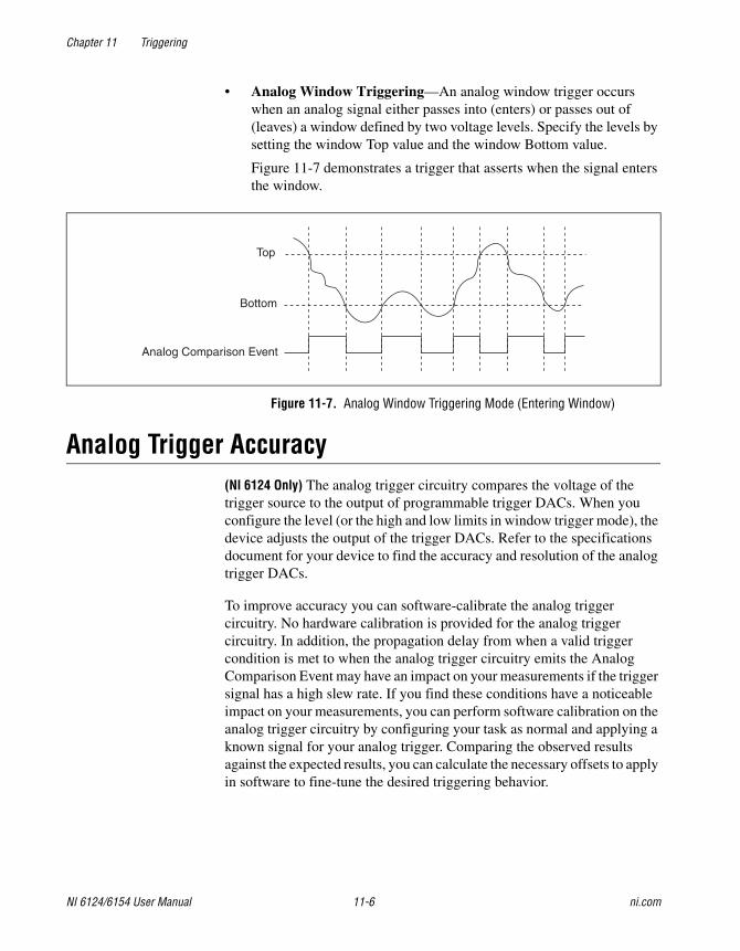
Chapter 11 Triggering
NI 6124/6154 User Manual 11-6 ni.com
• Analog Window Triggering—An analog window trigger occurs when an analog signal either passes into (enters) or passes out of (leaves) a window defined by two voltage levels. Specify the levels by setting the window Top value and the window Bottom value.
Figure 11-7 demonstrates a trigger that asserts when the signal enters the window.
Figure 11-7. Analog Window Triggering Mode (Entering Window)
Analog Trigger Accuracy(NI 6124 Only) The analog trigger circuitry compares the voltage of the trigger source to the output of programmable trigger DACs. When you configure the level (or the high and low limits in window trigger mode), the device adjusts the output of the trigger DACs. Refer to the specifications document for your device to find the accuracy and resolution of the analog trigger DACs.
To improve accuracy you can software-calibrate the analog trigger circuitry. No hardware calibration is provided for the analog trigger circuitry. In addition, the propagation delay from when a valid trigger condition is met to when the analog trigger circuitry emits the Analog Comparison Event may have an impact on your measurements if the trigger signal has a high slew rate. If you find these conditions have a noticeable impact on your measurements, you can perform software calibration on the analog trigger circuitry by configuring your task as normal and applying a known signal for your analog trigger. Comparing the observed results against the expected results, you can calculate the necessary offsets to apply in software to fine-tune the desired triggering behavior.
Top
Analog Comparison Event
Bottom
© National Instruments Corporation A-1 NI 6124/6154 User Manual
ADevice-Specific Information
This appendix includes device-specific information about the following S Series devices:
• NI 6124
• NI 6154
NI 6124The NI 6124 is a Plug-and-Play, multifunction analog, digital, and timing I/O device for PXI Express bus computers.
The NI 6124 features:
• Four simultaneously sampling analog inputs at 4 MS/s with one 16-bit A/D converter (ADC) per channel
• Two 16-bit D/A converters (DACs) with voltage outputs
• Eight lines of TTL-compatible correlated DIO
• 16 lines of TTL-compatible static DIO
• Two general-purpose 32-bit counter/timers
• Increased common-mode noise rejection through differential signal connection
Because the NI 6124 has no DIP switches, jumpers, or potentiometers, it can be easily calibrated and configured in software.
NI 6124 Analog OutputThe NI 6124 supplies two channels of AO voltage at the I/O connector. The range is fixed at bipolar ±10 V.
The AO channels on the NI 6124 contain 16-bit DACs that are capable of 4 MS/s for one channel or 2.5 MS/s for each of two channels. Refer to the NI 6124 Specifications for more detailed information about the AO capabilities of the NI 6124.
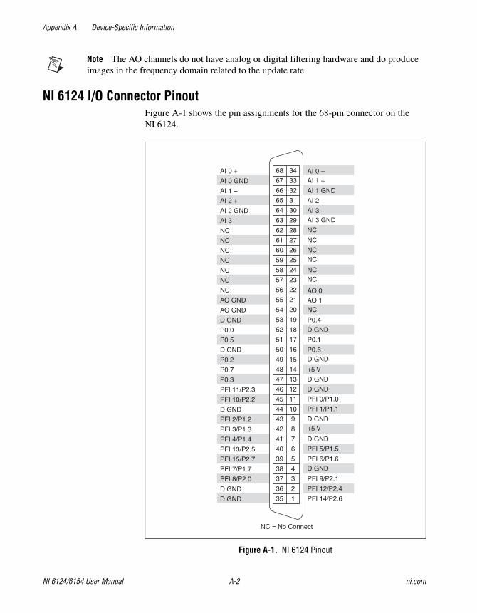
Appendix A Device-Specific Information
NI 6124/6154 User Manual A-2 ni.com
Note The AO channels do not have analog or digital filtering hardware and do produce images in the frequency domain related to the update rate.
NI 6124 I/O Connector PinoutFigure A-1 shows the pin assignments for the 68-pin connector on the NI 6124.
Figure A-1. NI 6124 Pinout
PFI 14/P2.6
PFI 12/P2.4
PFI 9/P2.1
D GND
PFI 6/P1.6
PFI 5/P1.5
D GND
+5 VD GND
PFI 1/P1.1
PFI 0/P1.0
D GND
D GND
+5 V
D GNDP0.6
P0.1
D GND
P0.4
NCAO 1
AO 0
NCNC
NCNC
NC
NC
AI 3 GNDAI 3 +
AI 2 –
AI 1 GND
AI 1 +AI 0 –
D GND
NC = No Connect
PFI 8/P2.0
PFI 7/P1.7
PFI 13/P2.5
PFI 4/P1.4
PFI 3/P1.3
PFI 2/P1.2
D GND
PFI 15/P2.7
D GND
PFI 10/P2.2
PFI 11/P2.3
P0.3
P0.7
P0.2
D GND
P0.5
P0.0
D GND
AO GND
AO GND
NC
NC
NC
NC
NC
NC
NC
AI 3 –
AI 2 GND
AI 2 +
AI 1 –
AI 0 GND
AI 0 +
135
236
337
438
539
640
741
842
943
1044
1145
1246
1347
1448
1549
1650
1751
1852
1953
2054
2155
2256
2357
2458
2559
2660
2761
2862
2963
3064
3165
3266
3367
3468
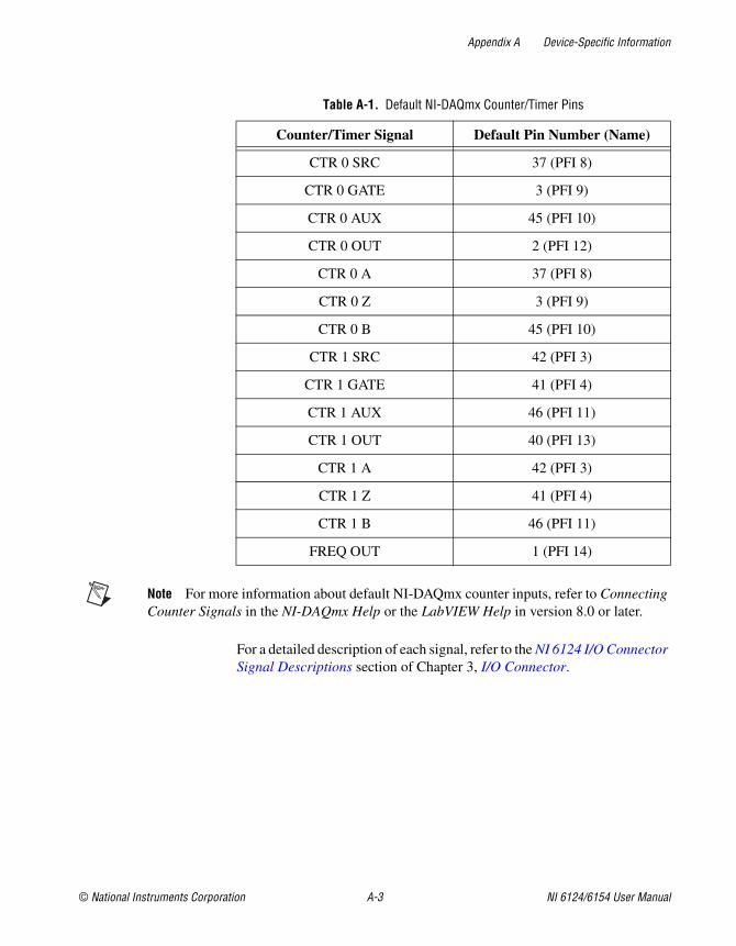
Appendix A Device-Specific Information
© National Instruments Corporation A-3 NI 6124/6154 User Manual
Note For more information about default NI-DAQmx counter inputs, refer to Connecting Counter Signals in the NI-DAQmx Help or the LabVIEW Help in version 8.0 or later.
For a detailed description of each signal, refer to the NI 6124 I/O Connector Signal Descriptions section of Chapter 3, I/O Connector.
Table A-1. Default NI-DAQmx Counter/Timer Pins
Counter/Timer Signal Default Pin Number (Name)
CTR 0 SRC 37 (PFI 8)
CTR 0 GATE 3 (PFI 9)
CTR 0 AUX 45 (PFI 10)
CTR 0 OUT 2 (PFI 12)
CTR 0 A 37 (PFI 8)
CTR 0 Z 3 (PFI 9)
CTR 0 B 45 (PFI 10)
CTR 1 SRC 42 (PFI 3)
CTR 1 GATE 41 (PFI 4)
CTR 1 AUX 46 (PFI 11)
CTR 1 OUT 40 (PFI 13)
CTR 1 A 42 (PFI 3)
CTR 1 Z 41 (PFI 4)
CTR 1 B 46 (PFI 11)
FREQ OUT 1 (PFI 14)
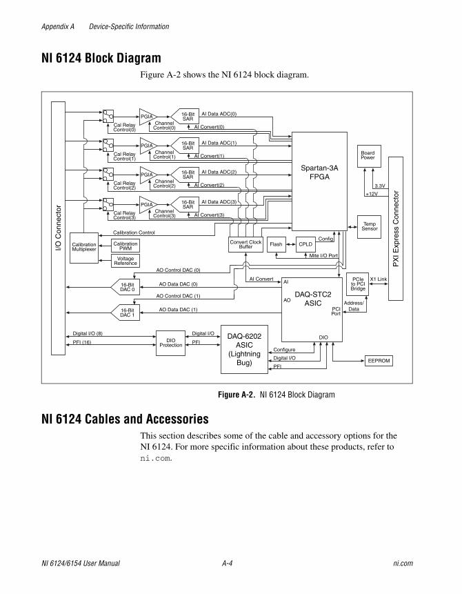
Appendix A Device-Specific Information
NI 6124/6154 User Manual A-4 ni.com
NI 6124 Block DiagramFigure A-2 shows the NI 6124 block diagram.
Figure A-2. NI 6124 Block Diagram
NI 6124 Cables and AccessoriesThis section describes some of the cable and accessory options for the NI 6124. For more specific information about these products, refer to ni.com.
Spartan-3AFPGA
BoardPower
TempSensor
PCIeto PCIBridge
PGIA AI Data ADC(0)
AI Convert(0)
16-BitSAR
ChannelControl(0)Cal Relay
Control(0)
PGIA AI Data ADC(1)
AI Convert(1)
16-BitSAR
ChannelControl(1)Cal Relay
Control(1)
PGIA AI Data ADC(2)
AI Convert(2)
16-BitSAR
ChannelControl(2)Cal Relay
Control(2)
PGIA AI Data ADC(3)
AI Convert(3)
16-BitSAR
ChannelControl(3)Cal Relay
Control(3)
Convert ClockBuffer Flash CPLD
ConfigCalibrationMultiplexer
Calibration Control
I/O C
onne
ctor
PX
I Exp
ress
Con
nect
or
CalibrationPWM
VoltageReference
16-BitDAC 0
DAQ-STC2ASIC
+12V
3.3V
Address/DataPCI
Port16-BitDAC 1
AI
AO
DIO
EEPROM
Configure
Digital I/O
PFI
DAQ-6202ASIC
(LightningBug)
AI Convert
DIOProtection
Digital I/O
PFI
Digital I/O (8)
PFI (16)
Mite I/O Port
AO Control DAC (0)
AO Data DAC (0)
AO Control DAC (1)
AO Data DAC (1)
X1 Link
Appendix A Device-Specific Information
© National Instruments Corporation A-5 NI 6124/6154 User Manual
Using BNCsYou can connect BNC cables to your DAQ device using BNC accessories such as the BNC-2110, BNC-2120, and BNC-2090A. To connect your DAQ device to a BNC accessory, use one of the following cables:
• SH68-68-EPM—shielded cable
• SH68-68R1-EP—shielded cable with one right angle connector
• SH6868—shielded 68-conductor cable
• RC68-68—unshielded cable
Using Screw TerminalsYou can connect signals to your DAQ device using a screw terminal accessory such as:
• CB-68LP, CB-68LPR—low-cost screw terminal block
• SCB-68—shielded screw terminal block with breadboard areas
• TBX-68—DIN rail mountable screw terminal block
To connect your DAQ device to a screw terminal accessory, use one of the following cables:
• SH68-68-EPM—shielded cable
• SH68-68R1-EP—shielded cable with one right angle connector
• RC68-68—unshielded cable
Using SSR or ER Digital Signal ConditioningSSR and ER series provide per channel digital signal conditioning.
Custom Cabling/Connectors OptionsThe CA-1000 is a versatile connector/enclosure system. It allows the user to define I/O connectors on a per-channel basis. Internally, the system allows for flexible custom wiring configuration.
If you want to develop your own cable, follow these guidelines for best results:
• Use shielded twisted-pair wires for each differential AI pair. Connect the shield for each signal pair to the ground reference at the source.
• Route the analog lines separately from the digital lines.
• When using a cable shield, use separate shields for the analog and digital halves of the cable. Failure to do so results in noise coupling into the analog signals from transient digital signals.
Appendix A Device-Specific Information
NI 6124/6154 User Manual A-6 ni.com
Mating connectors and a backshell kit for making custom 68-pin cables are available from NI.
NI recommends that you use one of the following connectors with the I/O connector on your device.
• Honda 68-position, solder cup, female connector
• Honda backshell
• AMP VHDCI connector
For more information about the connectors used for DAQ devices, refer to the KnowledgeBase document, Specifications and Manufacturers for Board Mating Connectors, by going to ni.com/info and entering the info code rdspmb.
NI 6124 SpecificationsRefer to the NI 6124 Specifications for more detailed information about the device.
Appendix A Device-Specific Information
© National Instruments Corporation A-7 NI 6124/6154 User Manual
NI 6154The NI 6154 is an isolated Plug-and-Play multifunction analog, digital, and timing I/O device for PCI bus computers.
The NI 6154 features:
• Four differential 16-bit analog inputs
• Four 16-bit analog output channels
• Ten lines of DIO (6 DI and 4 DO)
• Isolation for each AI and AO channel from the chassis and from one another
• Bank isolation for DIO from the chassis
Because the NI 6154 has no DIP switches, jumpers, or potentiometers, it can be easily calibrated and configured in software.
NI 6154 Analog OutputThe NI 6154 supplies four channels of AO voltage at the I/O connector. The range is fixed at bipolar ±10 V.
The AO channels on the NI 6154 contain 16-bit DACs that are capable of 250 kS/s for each channel. The AO channels are isolated from each other, from the AI channels, and from the chassis. Refer to the NI 6154 Specifications for more detailed information about the AO capabilities of the NI 6154.
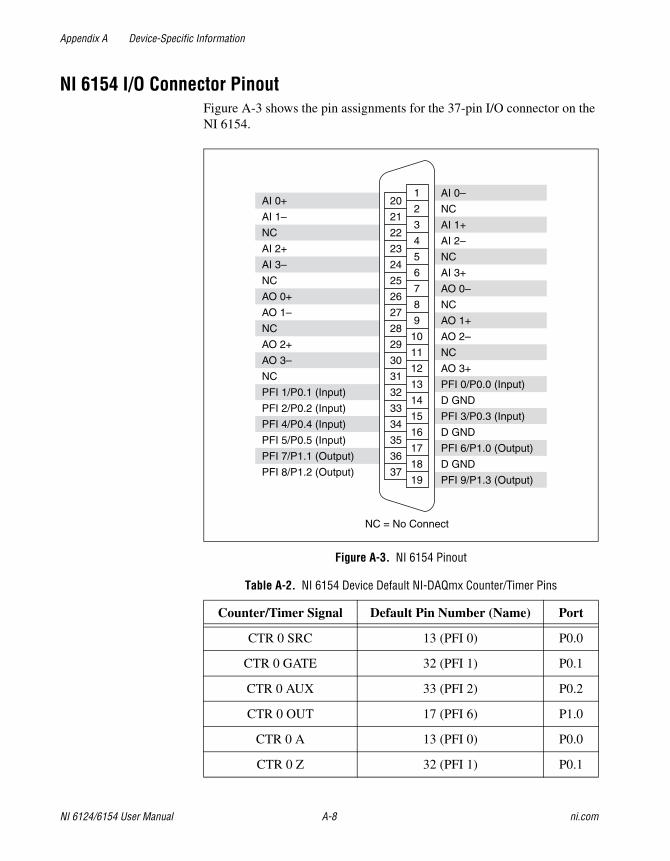
Appendix A Device-Specific Information
NI 6124/6154 User Manual A-8 ni.com
NI 6154 I/O Connector PinoutFigure A-3 shows the pin assignments for the 37-pin I/O connector on the NI 6154.
Figure A-3. NI 6154 Pinout
Table A-2. NI 6154 Device Default NI-DAQmx Counter/Timer Pins
Counter/Timer Signal Default Pin Number (Name) Port
CTR 0 SRC 13 (PFI 0) P0.0
CTR 0 GATE 32 (PFI 1) P0.1
CTR 0 AUX 33 (PFI 2) P0.2
CTR 0 OUT 17 (PFI 6) P1.0
CTR 0 A 13 (PFI 0) P0.0
CTR 0 Z 32 (PFI 1) P0.1
1
2
3
4
5
6
7
8
9
10
11
12
13
14
15
16
17
18
19
20
21
22
23
24
25
26
27
28
29
30
31
32
33
34
35
36
37
AI 0–
NC
AI 1+
AI 2–
NC
AI 3+
AO 0–
NC
AO 1+
AO 2–
NC
AO 3+
PFI 0/P0.0 (Input)
D GND
PFI 3/P0.3 (Input)
D GND
PFI 6/P1.0 (Output)
D GND
PFI 9/P1.3 (Output)
AI 0+
AI 1–
NC
AI 2+
AI 3–
NC
AO 0+
AO 1–
NC
AO 2+
AO 3–
NC
PFI 1/P0.1 (Input)
PFI 2/P0.2 (Input)
PFI 4/P0.4 (Input)
PFI 5/P0.5 (Input)
PFI 7/P1.1 (Output)
PFI 8/P1.2 (Output)
NC = No Connect
Appendix A Device-Specific Information
© National Instruments Corporation A-9 NI 6124/6154 User Manual
Note For more information about default NI-DAQmx counter inputs, refer to Connecting Counter Signals in the NI-DAQmx Help or the LabVIEW Help in version 8.0 or later.
For a detailed description of each signal, refer to the NI 6154 I/O Connector Signal Descriptions section of Chapter 3, I/O Connector.
CTR 0 B 33 (PFI 2) P0.2
CTR 1 SRC 15 (PFI 3) P0.3
CTR 1 GATE 34 (PFI 4) P0.4
CTR 1 AUX 35 (PFI 5) P0.5
CTR 1 OUT 36 (PFI 7) P1.1
CTR 1 A 15 (PFI 3) P0.3
CTR 1 Z 34 (PFI 4) P0.4
CTR 1 B 35 (PFI 5) P0.5
Table A-2. NI 6154 Device Default NI-DAQmx Counter/Timer Pins (Continued)
Counter/Timer Signal Default Pin Number (Name) Port
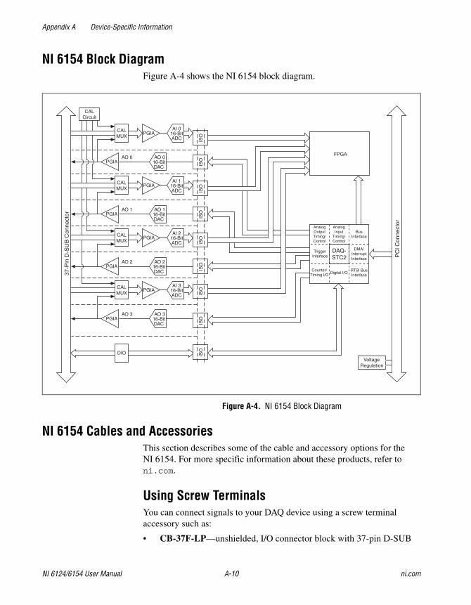
Appendix A Device-Specific Information
NI 6124/6154 User Manual A-10 ni.com
NI 6154 Block DiagramFigure A-4 shows the NI 6154 block diagram.
Figure A-4. NI 6154 Block Diagram
NI 6154 Cables and AccessoriesThis section describes some of the cable and accessory options for the NI 6154. For more specific information about these products, refer to ni.com.
Using Screw TerminalsYou can connect signals to your DAQ device using a screw terminal accessory such as:
• CB-37F-LP—unshielded, I/O connector block with 37-pin D-SUB
PGIA
PGIA
AI 016-BitADC
AO 016-BitDAC
CALMUX
CALCircuit
AO 0FPGA
VoltageRegulation
ISO
PGIA
PGIA
AI 116-BitADC
AO 116-BitDAC
CALMUX
AO 1
ISO
ISO
PGIA
PGIA
AI 216-BitADC
AO 216-BitDAC
CALMUX
AO 2
ISO
ISO
PGIA
PGIA
AI 316-BitADC
AO 316-BitDAC
CALMUX
DIO
AO 3
ISO
ISO
ISO
AnalogInput
Timing/Control
AnalogOutputTiming/Control
BusInterface
DAQ-STC2
TriggerInterface
Counter/Timing I/O Digital I/O
RTSI BusInterface
DMA/InterruptInterface
ISO
37-P
in D
-SU
B C
onne
ctor
PC
I Con
nect
or
Appendix A Device-Specific Information
© National Instruments Corporation A-11 NI 6124/6154 User Manual
• CB-37FH—37-pin screw terminal block, horizontal, DIN rail mount
• CB-37FV—37-pin screw terminal block, vertical, DIN rail mount
• TB-37F-37CP—37-pin crimp & poke terminals, shell with strain relief
• TB-37F-37SC—37-pin solder cup terminals, shell with strain relief
• CB-37F-HVD—37-pin screw terminal block, 150 V CAT II, DIN rail mount
To connect your DAQ device to a screw terminal accessory, use one of the following cables:
• SH37F-37M-2—37-pin female-to-male shielded I/O cable, 150 V, 2 m (non-EMI shielding)
• SH37F-37M-1—37-pin female-to-male shielded I/O cable, 150 V, 1 m (non-EMI shielding)
• SH37F-P-4—37-pin female-to-pigtails shielded I/O cable, 4 m
• R37F-37M-1—37-pin female-to-male ribbon I/O cable, 1 m1
• DB37M-DB37F-EP—37-pin male-to-female enhanced performance shielded I/O cable, 1 m (EMI shielding)
For more information about optional equipment available from National Instruments, refer to the National Instruments catalog or visit the National Instruments Web site at ni.com.
NI 6154 Isolation and Digital IsolatorsThe NI 6154 is an isolated data acquisition device. As shown in Figure 2-2, General NI 6124 Block Diagram, the analog input, analog output, and PFI/static DIO circuitry are referenced to separate isolated grounds for each circuit. The bus interface circuitry, RTSI, digital routing, and clock generation are all referenced to a non-isolated ground. Table A-3 shows the ground symbols referenced in Figure 2-2.
1 Not recommended for EMC-sensitive applications.
Table A-3. Ground Symbols
Ground Symbol
Isolated Ground
Non-Isolated Ground
Appendix A Device-Specific Information
NI 6124/6154 User Manual A-12 ni.com
The non-isolated ground is connected to the chassis ground of the PC or chassis where the device is installed.
The isolated ground is not connected to the chassis ground of the PC or chassis. The isolated ground can be at a higher or lower voltage relative to the non-isolated ground. All analog measurements are made relative to the isolated ground signal.
The isolated ground is an input to the NI 6154 device. The user must connect this ground to the ground of the system being measured or controlled. For more information, refer to the following:
• The Connecting Analog Input Signals section of Chapter 4, Analog Input
• Figure 4-2, Isolated S Series Analog Input Block Diagram
• The Connecting Analog Output Signals section of Chapter 5, Analog Output
• Figure 5-2, Isolated S Series Device Analog Output Block Diagram
• The Connecting Digital I/O Signals on Isolated Devices section of Chapter 6, Digital I/O
• Figure 6-5, Isolated S Series Devices Digital I/O Block Diagram
• Chapter 8, Programmable Function Interfaces (PFI)
Digital IsolationThe NI 6154 uses digital isolators. Unlike analog isolators, digital isolators do not introduce any analog error in the measurements taken by the device. The A/D converter, used for analog input, is on the isolated side of the device. The analog inputs are digitized before they are sent across the isolation barrier. Similarly, the D/A converters, used for analog output, are on the isolated side of the device.
Benefits of an Isolated DAQ DeviceWith isolation, engineers can safely measure a small voltage in the presence of a large common-mode signal. Some advantages of isolation are as follows:
• Improved rejection—Isolation increases the ability of the measurement system to reject common-mode voltages. Common-mode voltage is the signal that is present or “common” to both the positive and negative input of a measurement device, but is not part of the signal to be measured.
Appendix A Device-Specific Information
© National Instruments Corporation A-13 NI 6124/6154 User Manual
• Improved accuracy—Isolation improves measurement accuracy by physically preventing ground loops. Ground loops, a common source of error and noise, are the result of a measurement system having multiple grounds at different potentials.
• Improved safety—Isolation creates an insulation barrier so you can make floating measurements while protecting against large transient voltage spikes.
NI 6154 SpecificationsRefer to the NI 6154 Specifications for more detailed information about the device.
© National Instruments Corporation B-1 NI 6124/6154 User Manual
BTechnical Support and Professional Services
Visit the following sections of the award-winning National Instruments Web site at ni.com for technical support and professional services:
• Support—Technical support at ni.com/support includes the following resources:
– Self-Help Technical Resources—For answers and solutions, visit ni.com/support for software drivers and updates, a searchable KnowledgeBase, product manuals, step-by-step troubleshooting wizards, thousands of example programs, tutorials, application notes, instrument drivers, and so on. Registered users also receive access to the NI Discussion Forums at ni.com/forums. NI Applications Engineers make sure every question submitted online receives an answer.
– Standard Service Program Membership—This program entitles members to direct access to NI Applications Engineers via phone and email for one-to-one technical support as well as exclusive access to on demand training modules via the Services Resource Center. NI offers complementary membership for a full year after purchase, after which you may renew to continue your benefits.
For information about other technical support options in your area, visit ni.com/services, or contact your local office at ni.com/contact.
• Training and Certification—Visit ni.com/training for self-paced training, eLearning virtual classrooms, interactive CDs, and Certification program information. You also can register for instructor-led, hands-on courses at locations around the world.
• System Integration—If you have time constraints, limited in-house technical resources, or other project challenges, National Instruments Alliance Partner members can help. To learn more, call your local NI office or visit ni.com/alliance.
Appendix B Technical Support and Professional Services
NI 6124/6154 User Manual B-2 ni.com
• Declaration of Conformity (DoC)—A DoC is our claim of compliance with the Council of the European Communities using the manufacturer’s declaration of conformity. This system affords the user protection for electromagnetic compatibility (EMC) and product safety. You can obtain the DoC for your product by visiting ni.com/certification.
• Calibration Certificate—If your product supports calibration, you can obtain the calibration certificate for your product at ni.com/calibration.
If you searched ni.com and could not find the answers you need, contact your local office or NI corporate headquarters. Phone numbers for our worldwide offices are listed at the front of this manual. You also can visit the Worldwide Offices section of ni.com/niglobal to access the branch office Web sites, which provide up-to-date contact information, support phone numbers, email addresses, and current events.
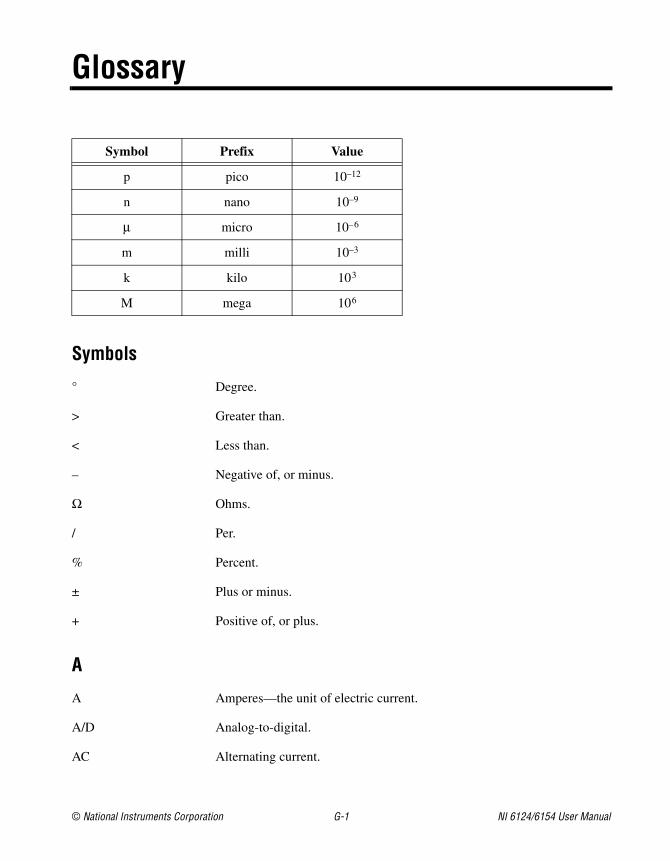
© National Instruments Corporation G-1 NI 6124/6154 User Manual
Glossary
Symbol Prefix Value
p pico 10–12
n nano 10–9
μ micro 10–6
m milli 10–3
k kilo 103
M mega 106
Symbols
° Degree.
> Greater than.
< Less than.
– Negative of, or minus.
Ω Ohms.
/ Per.
% Percent.
± Plus or minus.
+ Positive of, or plus.
A
A Amperes—the unit of electric current.
A/D Analog-to-digital.
AC Alternating current.
Glossary
NI 6124/6154 User Manual G-2 ni.com
ADC Analog-to-digital converter—an electronic device, often an integrated circuit, that converts an analog voltage to a digital number.
ADE Application Development Environment—a software environment incorporating the development, debug, and analysis tools for software development. LabVIEW, Measurement Studio, and Visual Studio are examples.
AI 1. Analog input.
2. Analog input channel signal.
aliasing The consequence of sampling that causes signals with frequencies higher than half the sampling frequency to appear as lower frequency components in a frequency spectrum.
AO Analog output.
ASIC Application-Specific Integrated Circuit—a proprietary semiconductor component designed and manufactured to perform a set of specific functions.
B
bipolar A signal range that includes both positive and negative values (for example, –5 to +5 V).
building ground See earth ground.
C
C Celsius
CalDAC Calibration DAC.
Glossary
© National Instruments Corporation G-3 NI 6124/6154 User Manual
channel 1. Physical—a terminal or pin at which you can measure or generate an analog or digital signal. A single physical channel can include more than one terminal, as in the case of a differential analog input channel or a digital port of eight lines. The name used for a counter physical channel is an exception because that physical channel name is not the name of the terminal where the counter measures or generates the digital signal.
2. Virtual—a collection of property settings that can include a name, a physical channel, input terminal connections, the type of measurement or generation, and scaling information. You can define NI-DAQmx virtual channels outside a task (global) or inside a task (local). Configuring virtual channels is integral to every measurement you take in NI-DAQmx. In NI-DAQmx, you can configure virtual channels either in MAX or in a program, and you can configure channels as part of a task or separately.
chassis ground Any connection back to the protective conductor earth ground. See also earth ground.
cm Centimeter.
CMOS Complementary metal-oxide semiconductor.
CMRR Common-mode rejection ratio—a measure of the capability of an instrument to reject a signal that is common to both input leads.
CompactPCI A Eurocard configuration of the PCI bus for industrial applications.
correlated DIO A feature that allows you to clock digital I/O on the same clock as analog I/O.
counter/timer A circuit that counts external pulses or clock pulses (timing).
coupling The manner in which a signal is connected from one circuit to another. When applied to instrument products or DAQ cards, it refers to the input signal coupling technique.
CTR Counter signal.
Glossary
NI 6124/6154 User Manual G-4 ni.com
D
D/A Digital-to-analog.
DAC Digital-to-analog converter—an electronic device, often an integrated circuit, that converts a digital number into a corresponding analog voltage or current.
DAQ See data acquisition (DAQ).
DAQ device A device that acquires or generates data and can contain multiple channels and conversion devices. DAQ devices include plug-in devices, PCMCIA cards, and DAQPad devices, which connect to a computer USB or 1394 (FireWire)® port. SCXI modules are considered DAQ devices.
DAQ-STC Data acquisition system timing controller—an application-specific integrated circuit (ASIC) for the system timing requirements of a general A/D and D/A system.
data acquisition (DAQ)
1. Acquiring and measuring analog or digital electrical signals from sensors, transducers, and test probes or fixtures.
2. Generating analog or digital electrical signals.
dB Decibel—the unit for expressing a logarithmic measure of the ratio of two signal levels: dB = 20log10 V1/V2 for signals in volts.
dBc Decibel carrier—level difference referenced to a carrier level, c.
DC Direct current—although the term speaks of current, many different types of DC measurements are made, including DC Voltage, DC current, and DC power.
device 1. An instrument or controller you can access as a single entity that controls or monitors real-world I/O points. A device often is connected to a host computer through some type of communication network.
2. See DAQ device.
DI Digital input.
DIFF Differential mode—an analog input mode consisting of two terminals, both of which are isolated from computer ground, whose difference is measured.
DIO Digital input/output.
Glossary
© National Instruments Corporation G-5 NI 6124/6154 User Manual
DIP Dual inline package.
DMA Direct memory access—a method by which data can be transferred to/from computer memory from/to a device or memory on the bus while the processor does something else. DMA is the fastest method of transferring data to/from computer memory.
DNL Differential nonlinearity—a measure in least significant bit of the worst-case deviation of code widths from their ideal value of 1 LSB.
DO Digital output.
driver Software unique to the device or type of device, and includes the set of commands the device accepts.
E
earth ground A direct electrical connection to the earth which provides a reference voltage level (called zero potential or ground potential) against which all other voltages in a system are established and measured. Also referred to as building ground.
EEPROM Electrically erasable programmable read–only memory–ROM that can be erased with an electrical signal and reprogrammed.
ESD Electrostatic Discharge—a high-voltage, low-current discharge of static electricity that can damage sensitive electronic components. Electrostatic discharge voltage can easily range from 1,000 to 10,000 V.
F
F Farad—a measurement unit of capacitance.
FIFO First-in-first-out memory buffer—a data buffering technique that functions like a shift register where the oldest values (first in) come out first. Many DAQ products use FIFOs to buffer digital data from an A/D converter, or to buffer the data before or after bus transmission.
floating signal sources
Signal sources with voltage signals that are not connected to an absolute reference of system ground. Also called nonreferenced signal sources. Some common examples of floating signal sources are batteries, transformers, and thermocouples.
Glossary
NI 6124/6154 User Manual G-6 ni.com
FPGA Field-programmable gate array.
G
gain The factor by which a signal is amplified, often expressed in dB. Gain as a function of frequency is commonly referred to as the magnitude of the frequency response function.
grounded signal sources
Signal sources with voltage sources that are referenced to a system ground such as the earth or building ground. Also called referenced signal sources.
H
h Hour.
Hz Hertz.
I
I/O Input/output—the transfer of data to/from a computer system involving communications channels, operator interface devices, and/or data acquisition and control interfaces.
in. Inches.
INL Integral nonlinearity—for an ADC, deviation of codes of the actual transfer function from a straight line.
IOH Current, output high.
IOL Current, output low.
IRQ Interrupt request.
L
LED Light-emitting diode—a semiconductor light source.
LSB Least significant bit.
Glossary
© National Instruments Corporation G-7 NI 6124/6154 User Manual
M
m Meter.
master A functional part of a MXI/VME/VXIbus device that initiates data transfers on the backplane. A transfer can be either a read or a write.
module A board assembly and its associated mechanical parts, front panel, optional shields, and so on. A module contains everything required to occupy one or more slots in a mainframe. SCXI and PXI devices are modules.
MSB Most significant bit.
mux Multiplexer—a switching device with multiple inputs that sequentially connects each of its inputs to its output, typically at high speeds, in order to measure several signals with a single analog input channel.
N
NC Normally closed, or not connected.
NI National Instruments.
NI-DAQmx The latest NI-DAQ driver with new VIs, functions, and development tools for controlling measurement devices. The advantages of NI-DAQmx over earlier versions of NI-DAQ include the DAQ Assistant for configuring channels and measurement tasks for your device for use in LabVIEW, LabWindows/CVI, and Measurement Studio; increased performance such as faster single-point analog I/O; and a simpler API for creating DAQ applications using fewer functions and VIs than earlier versions of NI-DAQ.
noise An undesirable electrical signal. Noise comes from external sources such as the AC power line, motors, generators, transformers, fluorescent lights, CRT displays, computers, electrical storms, welders, radio transmitters, and internal sources such as semiconductors, resistors, and capacitors. Noise corrupts signals you are trying to send or receive.
P
PCI Peripheral Component Interconnect—a high-performance expansion bus architecture originally developed by Intel to replace ISA and EISA. It offers a theoretical maximum transfer rate of 132 Mbytes/s.
Glossary
NI 6124/6154 User Manual G-8 ni.com
pd Pull-down.
PFI Programmable function interface.
PGIA Programmable gain instrumentation amplifier.
physical channel See channel.
port 1. A communications connection on a computer or a remote controller.
2. A digital port consisting of four or eight lines of digital input and/or output.
ppm Parts per million.
pu Pull-up.
PXI Express PCI Express eXtensions for Instrumentation—The PXI implementation of PCI Express, a scalable full-simplex serial bus standard that operates at 2.5 Gbps and offers both asynchronous and isochronous data transfers.
Q
quantization The process of converting an analog signal to a digital representation. Normally performed by an analog-to-digital converter (A/D converter or ADC).
R
range The maximum and minimum parameters between which a sensor, instrument, or device operates with a specified set of characteristics.
referenced signal sources
Signal sources with voltage signals that are referenced to a system ground such as the earth or a building ground. Also called ground signal sources.
rise time The time for a signal to transition from 10% to 90% of the maximum signal amplitude.
rms Root mean square.
RTSI bus Real-Time System Integration bus—the National Instruments timing bus that connects DAQ devices directly, by means of connectors on top of the devices, for precise synchronization of functions.
Glossary
© National Instruments Corporation G-9 NI 6124/6154 User Manual
S
s Seconds.
S Samples.
S/s Samples per second—used to express the rate at which a digitizer or D/A converter or DAQ device samples an analog signal.
scatter-gather The term used to describe very high-speed DMA burst-mode transfers that are made only by the bus master, and where noncontiguous blocks of memory are transparently mapped by the controller to appear as a seamless piece of memory.
SCXI Signal Conditioning eXtensions for Instrumentation—the National Instruments product line for conditioning low-level signals within an external chassis near sensors so that only high-level signals are sent to DAQ devices in the noisy PC environment. SCXI is an open standard available for all vendors.
sensor A device that responds to a physical stimulus (heat, light, sound, pressure, motion, flow, and so on) and produces a corresponding electrical signal.
settling time The amount of time required for a voltage to reach its final value within specified limits.
signal conditioning The manipulation of signals to prepare them for digitizing.
SOURCE Source signal.
system noise A measure of the amount of noise seen by an analog circuit or an ADC when the analog inputs are grounded.
T
task NI-DAQmx—a collection of one or more channels, timing, and triggering and other properties that apply to the task itself. Conceptually, a task represents a measurement or generation you want to perform.
terminal count The highest value of a counter.
tgh Gate hold time.
tgsu Gate setup time.
Glossary
NI 6124/6154 User Manual G-10 ni.com
tgw Gate pulse width.
THD Total harmonic distortion—the ratio of the total rms signal due to harmonic distortion to the overall rms signal, in dB or percent.
THD+N Signal-to-THD plus noise—the ratio in decibels of the overall rms signal to the rms signal of harmonic distortion, plus noise introduced.
thermocouple A temperature sensor created by joining two dissimilar metals. The junction produces a small voltage as a function of the temperature.
toff An offset (delayed) pulse; the offset is t nanoseconds from the falling edge of the AI CONV CLK* signal.
tout Output delay time.
tp Period of a pulse train.
transducer See sensor.
tsc Source clock period.
tsp Source pulse width.
TTL Transistor-transistor logic—a digital circuit composed of bipolar transistors wired in a certain manner. A typical medium-speed digital technology. Nominal TTL logic levels are 0 and 5 V.
V
V Volts.
VCC Nominal +5 V power supply provided by the PC motherboard.
Vcm Common-mode noise and ground potential.
VDC Volts direct current.
VI, virtual instrument 1. A combination of hardware and/or software elements, typically used with a PC, that has the functionality of a classic stand-alone instrument.
2. A LabVIEW software module (VI), which consists of a front panel user interface and a block diagram program.
VIH Volts, input high.
Glossary
© National Instruments Corporation G-11 NI 6124/6154 User Manual
VIL Volts, input low.
Vin Volts in.
Vm Measured voltage.
VOH Volts, output high.
VOL Volts, output low.
VOUT Volts out.
Vrms Volts, root mean square.
Vs Ground-referenced signal source.
virtual channel See channel.
© National Instruments Corporation I-1 NI 6124/6154 User Manual
Index
Numerics10 MHz reference clock, 9-3100 kHz Timebase, 9-220 MHz Timebase, 9-280 MHz source mode, 7-3880 MHz Timebase, 9-2
AA/D converter, 4-2AC coupling connections, 4-9accessories
field wiring considerations, 4-11I/O connector, 3-1NI 6124, A-4NI 6154, A-10
acquisitions, digital waveform, 6-3AI Convert Clock signal, 4-16AI Convert Clock Timebase signal, 4-17AI Reference Trigger signal, 4-19AI Sample Clock signal, 4-14AI Sample Clock Timebase signal, 4-16AI Start Trigger signal, 4-18ai/ConvertClock, 4-16ai/ConvertClockTimebase, 4-17ai/ReferenceTrigger, 4-19ai/SampleClock, 4-14ai/SampleClockTimebase, 4-16ai/StartTrigger, 4-18analog edge triggering, 11-3
with hysteresis, 11-4analog input
circuitry, 4-2data acquisition methods, 4-4fundamentals, 4-1overview, 4-1
signalsAI Convert Clock, 4-16AI Convert Clock Timebase, 4-17AI Reference Trigger, 4-19AI Sample Clock, 4-14AI Sample Clock Timebase, 4-16AI Start Trigger, 4-18connecting, 4-6
terminal configuration, 4-2timing signals, 4-13timing summary, 4-13triggering, 4-6
analog outputcircuitry, 5-2connecting signals, 5-4data generation methods, 5-2fundamentals, 5-1minimizing glitches, 5-2NI 6124, A-1NI 6154, A-7overview, 5-1triggering, 5-4
analog output signalsAO Pause Trigger, 5-10AO Sample Clock, 5-6AO Sample Clock Timebase, 5-8AO Start Trigger, 5-9
analog triggeringabout, 11-2accuracy, 11-6types, 11-3
analog window triggering, 11-6ANSI C documentation, xivAO Pause Trigger signal, 5-10AO Sample Clock signal, 5-6AO Sample Clock Timebase signal, 5-8AO Start Trigger signal, 5-9
Index
NI 6124/6154 User Manual I-2 ni.com
applicationscounter input, 7-2counter output, 7-19edge counting, 7-2
arm start trigger, 7-31
Bblock diagram
NI 6124, A-4NI 6154, A-10PFI input circuitry, 8-3PFI output circuitry, 8-3
bufferededge counting, 7-3period measurement, 7-7position measurement, 7-17pulse-width measurement, 7-5semi-period measurement, 7-8two-signal edge-separation
measurement, 7-18bus
interface, 10-1RTSI, 9-4
Ccables
NI 6124, A-4NI 6154, A-10
calibration, 1-2, 2-4calibration certificate (NI resources), B-2cascading counters, 7-32Change Detection Event signal, 6-8channel
Z behavior, 7-15choosing frequency measurement, 7-12clock
10 MHz reference, 9-3external reference, 9-2generation, 9-1
PXI, and trigger signals, 9-8routing, 9-1
common-modeinput range, 4-3noise
differential ground-referenced signals, 4-9
differential non-referenced or floating signals, 4-11
differential signals, 4-9rejection, 4-11
signal rangedifferential non-referenced or
floating signals, 4-9signal rejection considerations
differential ground-referenced signals, 4-9
connectingdigital I/O signals, 6-9PFI input signals, 8-6
connecting signalsanalog input, 4-6analog output, 5-4digital I/O
S Series isolated devices (NI 6154), 6-12
S Series non-isolated devices (NI 6124), 6-9
continuous pulse train generation, 7-21controlling counting direction, 7-2conventions used in the manual, xicounter
input and output, 7-30output applications, 7-19terminals, default, 7-30
Counter n A signal, 7-28Counter n Aux signal, 7-28Counter n B signal, 7-28Counter n Gate signal, 7-27Counter n HW Arm signal, 7-29Counter n Internal Output signal, 7-29
Index
© National Instruments Corporation I-3 NI 6124/6154 User Manual
Counter n Source signal, 7-26Counter n TC signal, 7-29Counter n Up_Down signal, 7-29Counter n Z signal, 7-28counter signals
Counter n A, 7-28Counter n Aux, 7-28Counter n B, 7-28Counter n Gate, 7-27Counter n HW Arm, 7-29Counter n Internal Output, 7-29Counter n Source, 7-26Counter n TC, 7-29Counter n Up_Down, 7-29FREQ OUT, 7-30Frequency Output, 7-30
counters, 7-1cascading, 7-32connecting terminals, 7-30duplicate count prevention, 7-34edge counting, 7-2filters, 7-32generation, 7-19input applications, 7-2other features, 7-32output applications, 7-19prescaling, 7-33pulse train generation, 7-21retriggerable single pulse
generation, 7-20simple pulse generation, 7-19single pulse generation, 7-19single pulse generation with start
trigger, 7-20synchronization modes, 7-37timing signals, 7-25triggering, 7-31
counting edges, 7-2
DDAC FIFO, 5-2DACs, 5-2DAQ
hardware for isolated devices, 2-3hardware for non-isolated devices, 2-2system overview, 2-1
DAQ-PnP, 10-1DAQ-STC2, 2-3data generation methods, 5-2data transfer methods, changing, 10-2DC coupling
connections, 4-9Declaration of Conformity (NI resources), B-2default
counter terminals, 7-30NI-DAQmx counter/timer pins, 7-30pins, 7-30
devicemultiple synchronization, 9-3pinouts, 1-3specifications, 1-3
DI change detection, 6-8DI Sample Clock signal, 6-4di/SampleClock, 6-4diagnostic tools (NI resources), B-1DIFF mode
about, 4-2connections for ground-referenced signal
sources, 4-7connections for non-referenced or
floating signal sources, 4-9minimizing drift, 4-12
differential connectionsfor ground-referenced signal sources, 4-7,
4-11for non-referenced or floating signal
sources, 4-9digital
isolation (NI 6154), A-12
Index
NI 6124/6154 User Manual I-4 ni.com
triggering, 11-1waveform acquisition, 6-3waveform generation, 6-5
digital I/O, 6-1block diagram, 6-2circuitry, 6-2connecting signals, 6-9DI change detection, 6-8digital waveform generation, 6-5getting started with applications in
software, 6-10I/O protection, 6-7programmable power-up states, 6-7static DIO, 6-2waveform acquisition, 6-3waveform triggering, 6-3
digital I/O for isolated devicesconnecting signals, 6-9, 6-12I/O protection, 6-12software, 6-13static DIO, 6-11
digital routing, 9-1digital signals
Change Detection Event, 6-8connecting, 6-9DI Sample Clock, 6-4DO Sample Clock, 6-5
digital waveformacquisition, 6-3generation, 6-5
direct memory access (DMA), 10-2DMA, 10-2DO Sample Clock signal, 6-5do/SampleClock, 6-5documentation
conventions used in manual, xiNI resources, B-1related documentation, xii
drivers (NI resources), B-1duplicate count prevention, 7-34
enabling in NI-DAQmx, 7-37
example, 7-35prevention example, 7-36
Eedge counting, 7-2
buffered, 7-3on-demand, 7-2sample clock, 7-3single point, 7-2
edge-separation measurementbuffered two-signal, 7-18single two-signal, 7-18
enabling duplicate count prevention in NI-DAQmx, 7-37
encoders, quadrature, 7-14encoding
X1, 7-14X2, 7-15X4, 7-15
equivalent time sampling, 7-24examples (NI resources), B-1exporting timing output signals using PFI
terminals, 8-4external reference clock, 9-2external source mode, 7-39
Ffeatures
counter, 7-32NI 6124, A-1NI 6154, A-7
field wiring considerations, 4-11FIFO, 4-2filter, 4-2filters
counter, 7-32PFI, 8-6PXI_STAR, 9-9RTSI, 9-6
Index
© National Instruments Corporation I-5 NI 6124/6154 User Manual
finite pulse train timing generation, 7-22FREQ OUT signal, 7-30frequency
division, 7-24generation, 7-23generator, 7-23measurement, 7-9
Frequency Output signal, 7-30
Ggenerations
clock, 9-1continuous pulse train, 7-21digital waveform, 6-5frequency, 7-23pulse for ETS, 7-24pulse train, 7-21retriggerable single pulse, 7-20simple pulse, 7-19single pulse, 7-19single pulse with start trigger, 7-20
getting started, 1-1DIO applications in software, 6-10
glitches, 5-2
Hhardware, 1-2help, technical support, B-1hysteresis, analog edge triggering with, 11-4
II/O connector
NI 6124, A-2NI 6154, A-8signal descriptions
isolated devices, 3-2non-isolated devices, 3-1
I/O protection, 6-7, 8-8input coupling, 4-2input polarity and range, 4-3input signals
using PFI terminals as, 8-4using RTSI terminals as, 9-6
installationhardware, 1-2NI-DAQmx, 1-1other software, 1-1
instrument drivers (NI resources), B-1instrumentation amplifier, 4-2interrupt request (IRQ), 10-2IRQ, 10-2isolation (NI 6154), A-11
digital isolation, A-12
KKnowledgeBase, B-1
LLabVIEW documentation, xiiLabWindows/CVI documentation, xiii
MMeasurement Studio documentation, xiiimeasurements
buffered period, 7-7buffered pulse-width, 7-5buffered semi-period, 7-8buffered two-signal edge-separation, 7-18choosing frequency, 7-12frequency, 7-9period, 7-6position, 7-14pulse-width, 7-4semi-period, 7-7single period, 7-6
Index
NI 6124/6154 User Manual I-6 ni.com
single pulse-width, 7-4single semi-period, 7-8single two-signal edge-separation, 7-18two-signal edge-separation, 7-17using quadrature encoders, 7-14using two pulse encoders, 7-16
measuringhigh frequency with two counters, 7-10large range of frequencies using two
counters, 7-11low frequency with one counter, 7-9
averaged, 7-9minimizing glitches on the output signal, 5-2MITE and DAQ-PnP, 10-1multiple device synchronization, 9-3mux, 4-2
NNational Instruments support and
services, B-1.NET languages documentation, xivNI 6124, A-4
analog output, A-1block diagram, A-4cables and accessories, A-4features, A-1I/O connector pinout, A-2specifications, A-6
NI 6154, A-10block diagram, A-10cables and accessories, A-10digital I/O, 6-11features, A-7I/O connector pinout, A-8isolation and digital isolators, A-11isolation barrier and digital isolators, 4-2,
5-2specifications, A-13working voltage range, 4-4
NI support and services, B-1
NI-DAQmxdefault counter terminals, 7-30documentation, xiienabling duplicate count prevention, 7-37
Oon-demand edge counting, 7-2other
internal source mode, 7-39software, installing, 1-1
outputs, using RTSI as, 9-5
Ppause trigger, 7-31period measurement, 7-6
buffered, 7-7single, 7-6
PFI, 8-1, 8-2connecting input signals, 8-6exporting timing output signals using PFI
terminals, 8-4filters, 8-6I/O protection, 8-8programmable power-up states, 8-8, 8-9using terminals as static digital I/Os, 8-5using terminals as timing input
signals, 8-4PFI terminals as static digital I/Os, 8-5pinouts
counter default, 7-30device, 1-3NI 6124, A-2NI 6154, A-8RTSI connector, 9-4
pins, default, 7-30polarity and reference selection, 5-2position measurement, 7-14
buffered, 7-17power source, 3-3
Index
© National Instruments Corporation I-7 NI 6124/6154 User Manual
power-up states, 6-7, 8-8, 8-9prescaling, 7-33programmable
function interface (PFI), 8-1power-up states, 6-7, 8-8
programmable function interface, 8-2programmable power-up states, 8-9programmed I/O, 10-2programming examples (NI resources), B-1pulse
encoders, 7-16generation for ETS, 7-24train generation, 7-21
continuous, 7-21pulse-width measurement, 7-4
buffered, 7-5single, 7-4
PXIand PXI Express, 10-1clock, 10-1clock and trigger signals, 9-8trigger signals, 10-1triggers, 9-8
PXI Expressand PXI, 10-1chassis compatibility, 10-1
PXI_CLK10, 9-8PXI_STAR
filters, 9-9trigger, 9-8
Qquadrature encoders, 7-14
Rreal-time system integration bus, 9-4reciprocal frequency measurement, 7-11
referenceclock
10 MHz, 9-3external, 9-2
related documentation, xiiretriggerable single pulse generation, 7-20routing
clock, 9-1digital, 9-1
RTSI, 9-4connector pinout, 9-4filters, 9-6using as outputs, 9-5using terminals as timing input
signals, 9-6
SS Series
devices, A-1specifications, xv
sample clockedge counting, 7-3
sample clock measurement, 7-17self-calibration, 1-2semi-period measurement, 7-7
buffered, 7-8single, 7-8
sensors, 2-5signal conditioning, 2-5signal connections
analog input, 4-6analog output, 5-4digital I/O for isolated devices, 6-12
signal descriptionsS Series isolated devices (NI 6154), 3-2S Series non-isolated devices
(NI 6124), 3-1signal routing, RTSI bus, 9-4signal sources, 4-7
Index
NI 6124/6154 User Manual I-8 ni.com
signalsAI Convert Clock, 4-16AI Convert Clock Timebase, 4-17AI Reference Trigger, 4-19AI Sample Clock, 4-14AI Sample Clock Timebase, 4-16AI Start Trigger, 4-18Change Detection Event, 6-8connecting digital I/O, 6-9connecting PFI input, 8-6Counter n A, 7-28Counter n Aux, 7-28Counter n B, 7-28Counter n Gate, 7-27Counter n HW Arm, 7-29Counter n Internal Output, 7-29Counter n Source, 7-26Counter n TC, 7-29Counter n Up_Down, 7-29Counter n Z, 7-28counters, 7-25DI Sample Clock, 6-4DO Sample Clock, 6-5exporting timing output using PFI
terminals, 8-4FREQ OUT, 7-30Frequency Output, 7-30
simple pulse generation, 7-19single
period measurement, 7-6point edge counting, 7-2pulse generation, 7-19
retriggerable, 7-20with start trigger, 7-20
pulse-width measurement, 7-4semi-period measurement, 7-8two-signal edge-separation
measurement, 7-18
software, 1-1AI applications, 4-21AO applications, 5-11DIO applications for isolated
devices, 6-13NI resources, B-1programming devices, 2-6routing signals in, 9-10
specificationsdevice, 1-3NI 6124, A-6NI 6154, A-13
start trigger, 7-31static DIO, 6-2
S Series isolated devices (NI 6154), 6-11using PFI terminals as, 8-5
support, technical, B-1synchronization modes, 7-37
80 MHz source, 7-38external source, 7-39other internal source, 7-39
synchronizing multiple devices, 9-3synchronous counting mode, 7-34system timing controller
DAQ-STC2 (isolated devices), 2-3
Ttechnical support, xv, B-1terminals
connecting counter, 7-30NI-DAQmx default counter, 7-30
Timebase100 kHz, 9-220 MHz, 9-280 MHz, 9-2
timing output signals, exporting using PFI terminals, 8-4
timing signalswaveform generation, 5-6
training, xv
Index
© National Instruments Corporation I-9 NI 6124/6154 User Manual
training and certification (NI resources), B-1transducers, 2-5trigger
arm start, 7-31pause, 7-31PXI, 9-8PXI_STAR, 9-8Star Trigger, 9-8start, 7-31
triggeringanalog edge, 11-3analog edge with hysteresis, 11-4analog input, 4-6analog output, 5-4analog types, 11-3analog window, 11-6counter, 7-31digital waveform, 6-3overview, 11-1with a digital source, 11-1with an analog source, 11-2
troubleshooting (NI resources), B-1two-signal edge-separation
measurement, 7-17buffered, 7-18single, 7-18
types of analog triggers, 11-3
Uusing
PFI terminalsas static digital I/Os, 8-5as timing input signals, 8-4to export timing output signals, 8-4
RTSIas outputs, 9-5terminals as timing input signals, 9-6
using PFI terminalsas static digital I/Os, 8-5
Wwaveform
generationdigital, 6-5
triggering, 6-3waveform generation timing signals
AO Pause Trigger, 5-10AO Sample Clock, 5-6AO Sample Clock Timebase, 5-8AO Start Trigger, 5-9summary, 5-6
Web resources, B-1wiring, 4-11working voltage range, 4-4
XX1 encoding, 7-14X2 encoding, 7-15X4 encoding, 7-15


![Phys 6124 zipped!predrag/courses/PHYS-6124-19/week1.pdf · Optional reading: Stone & GoldbartAppendix A; Arfken & Weber Arfken and Weber [1] Chapter 3 Feel free to add your topics](https://img.pdfslide.us/doc/110x75/5e889e793019b942d41e3f17/phys-6124-zipped-predragcoursesphys-6124-19week1pdf-optional-reading-stone.jpg)