Embed Size (px)
Citation preview
New SSD Interfaces and Their Impact on SSD Controller Architecture
Tim Canepa Director of Architecture
LSI Flash Components Division, an Avago Company
Flash Memory Summit 2014 Santa Clara, CA
1
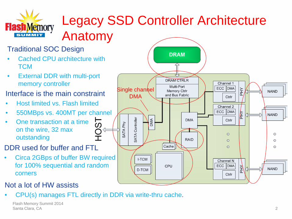
Legacy SSD Controller Architecture Anatomy
Flash Memory Summit 2014 Santa Clara, CA
2
Traditional SOC Design • Cached CPU architecture with
TCM • External DDR with multi-port
memory controller Interface is the main constraint • Host limited vs. Flash limited • 550MBps vs. 400MT per channel
• One transaction at a time on the wire, 32 max outstanding
DDR used for buffer and FTL • Circa 2GBps of buffer BW required
for 100% sequential and random corners
Not a lot of HW assists • CPU(s) manages FTL directly in DDR via write-thru cache.
Single channel DMA
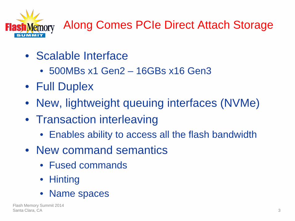
Along Comes PCIe Direct Attach Storage
• Scalable Interface • 500MBs x1 Gen2 – 16GBs x16 Gen3
• Full Duplex • New, lightweight queuing interfaces (NVMe) • Transaction interleaving
• Enables ability to access all the flash bandwidth • New command semantics
• Fused commands • Hinting • Name spaces
Flash Memory Summit 2014 Santa Clara, CA
3
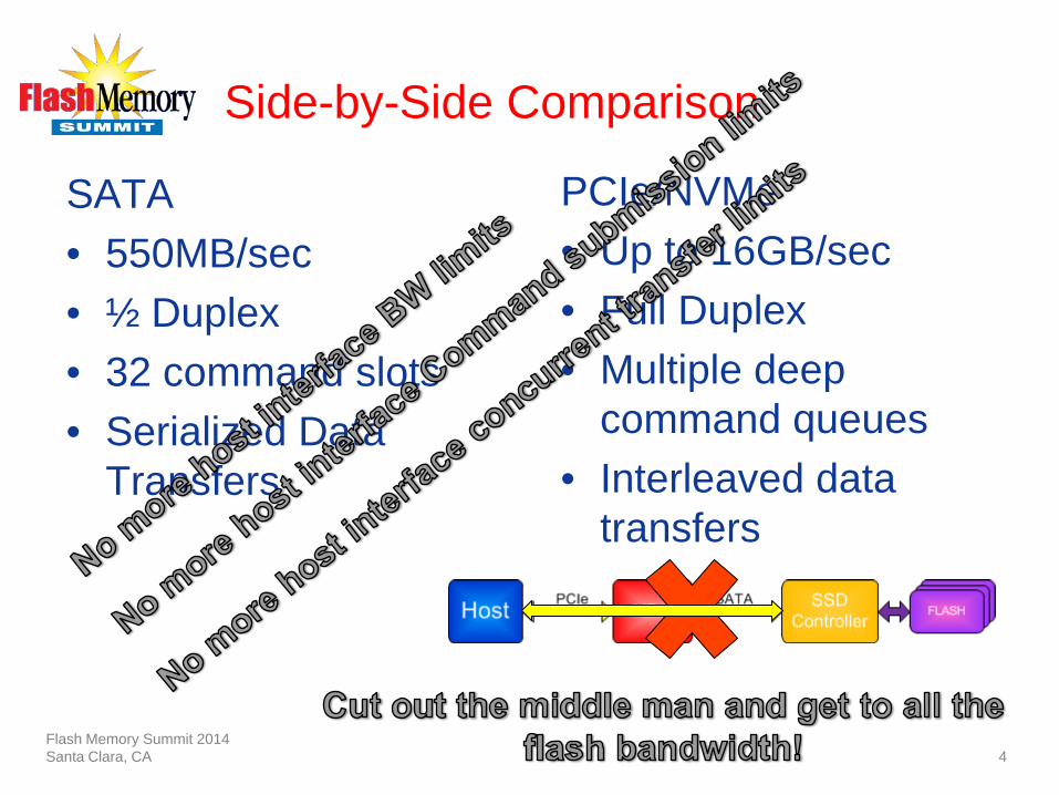
Side-by-Side Comparison
SATA • 550MB/sec • ½ Duplex • 32 command slots • Serialized Data
Transfers
Flash Memory Summit 2014 Santa Clara, CA
4
PCIe/NVMe • Up to 16GB/sec • Full Duplex • Multiple deep
command queues • Interleaved data
transfers

Legacy SSD Controller Architectures (bottle necks)
Flash Memory Summit 2014 Santa Clara, CA
5
8 channels of ONFI 3.0 can source 3.2GBps
Bottleneck 1: DDR buffer BW • Need well in excess of
6.4GBps to service flash alone.
• 32Bit DDR3 1600 won’t even cut it
1
Bottleneck 2: Flash Data path • DMA needs to be multi-channel
to keep all channels active. • Bus BW needs to increase to
>3.2GBps
2
2 • Wider or faster DDR
I/F is not attractive (power & cost)
Legacy SSD Controller Architectures (bottle necks - continued)
Flash Memory Summit 2014 Santa Clara, CA
6
8 channels of ONFI 3.0 can source 3.2GBps
Bottleneck 3: Host I/F DMA & Data Path
Bottleneck 4: Processor complex • Direct FTL management in DDR
becomes prohibitive. • More IOPs require more MIPs
and more context tracking
• Requires multi-channel DMA to interleave data for multiple requests. If not, transaction tenure will increase as will
• requires well in excess of 3.2GBps of BW
3
4
4
Flash Memory Summit 2014 Santa Clara, CA
7
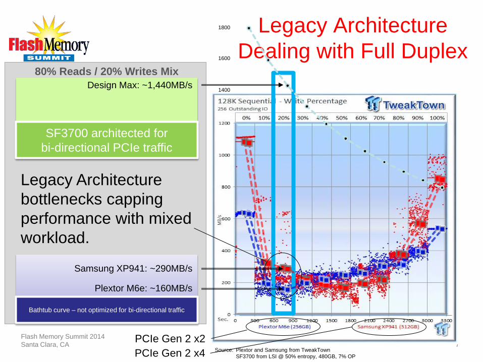
1400
1600
1800 1,800MB/s Sequential
Reads
Source: Plextor and Samsung from TweakTown SF3700 from LSI @ 50% entropy, 480GB, 7% OP
Legacy Architecture Dealing with Full Duplex
PCIe Gen 2 x4
Bathtub curve – not optimized for bi-directional traffic
Plextor M6e: ~160MB/s
Samsung XP941: ~290MB/s
80% Reads / 20% Writes Mix
SF3700 architected for bi-directional PCIe traffic
Design Max: ~1,440MB/s
PCIe Gen 2 x2
Legacy Architecture
bottlenecks capping performance with mixed workload.

How is Throughput Determined? • Throughput is influenced by many factors
• Flash die limits – a 1TB drive can produce16GBps of read BW • Flash channel limits • Internal B/W limits (e.g., buffers, compression engines, etc) • Tenures – how long are resources held before they can be reused • Host I/F limits • CPU limits
• What’s key is understand what the limiting factor(s) is(are) • And at what range of parameters, as the limiting factor(s) may
vary • And how to strike a balance to get the best performance in all
corners
Flash Memory Summit 2014 Santa Clara, CA
8
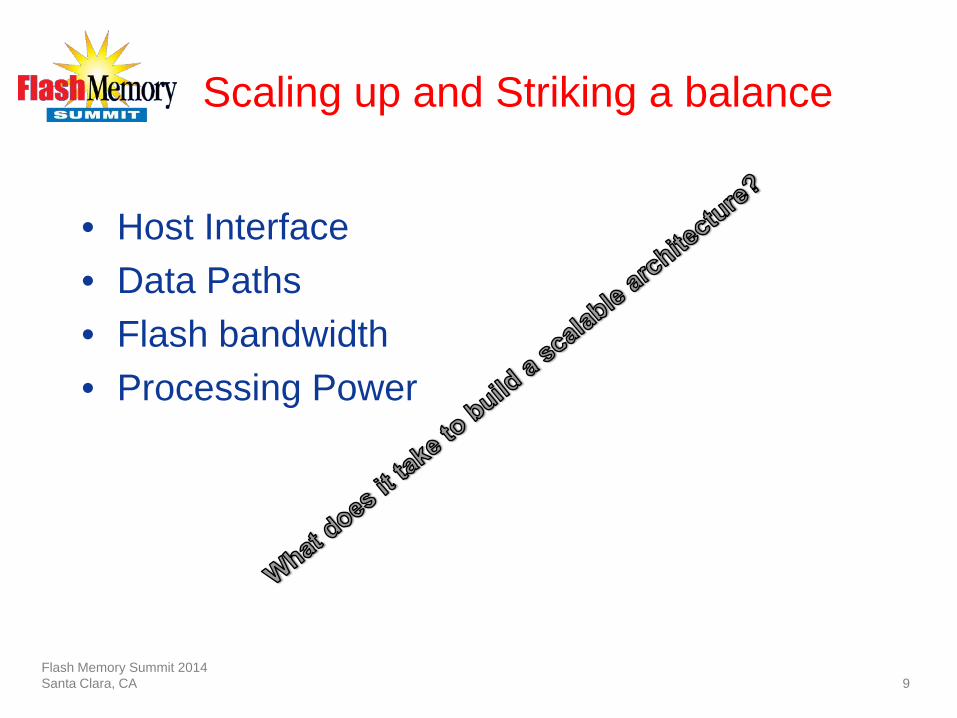
Scaling up and Striking a balance
• Host Interface • Data Paths • Flash bandwidth • Processing Power
Flash Memory Summit 2014 Santa Clara, CA
9
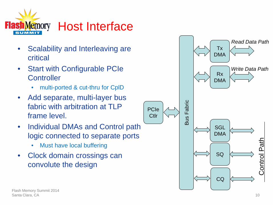
Host Interface
• Scalability and Interleaving are critical
• Start with Configurable PCIe Controller
• multi-ported & cut-thru for CplD
• Add separate, multi-layer bus fabric with arbitration at TLP frame level.
• Individual DMAs and Control path logic connected to separate ports
• Must have local buffering
• Clock domain crossings can convolute the design
Flash Memory Summit 2014 Santa Clara, CA
10
PCIe Ctlr
Bus
Fabr
ic
Tx DMA
Read Data Path
Rx DMA
SQ
CQ
SGL DMA
Write Data Path
Con
trol P
ath
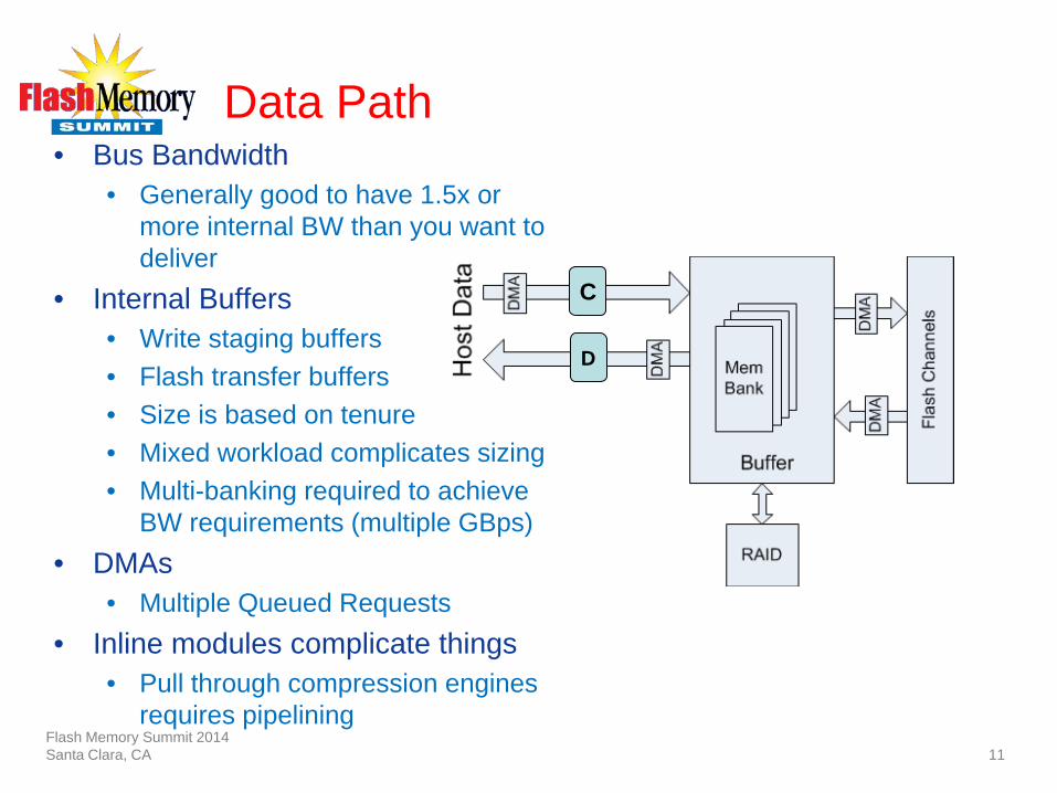
Data Path • Bus Bandwidth
• Generally good to have 1.5x or more internal BW than you want to deliver
• Internal Buffers • Write staging buffers • Flash transfer buffers • Size is based on tenure • Mixed workload complicates sizing • Multi-banking required to achieve
BW requirements (multiple GBps) • DMAs
• Multiple Queued Requests • Inline modules complicate things
• Pull through compression engines requires pipelining
Flash Memory Summit 2014 Santa Clara, CA
11
C
D
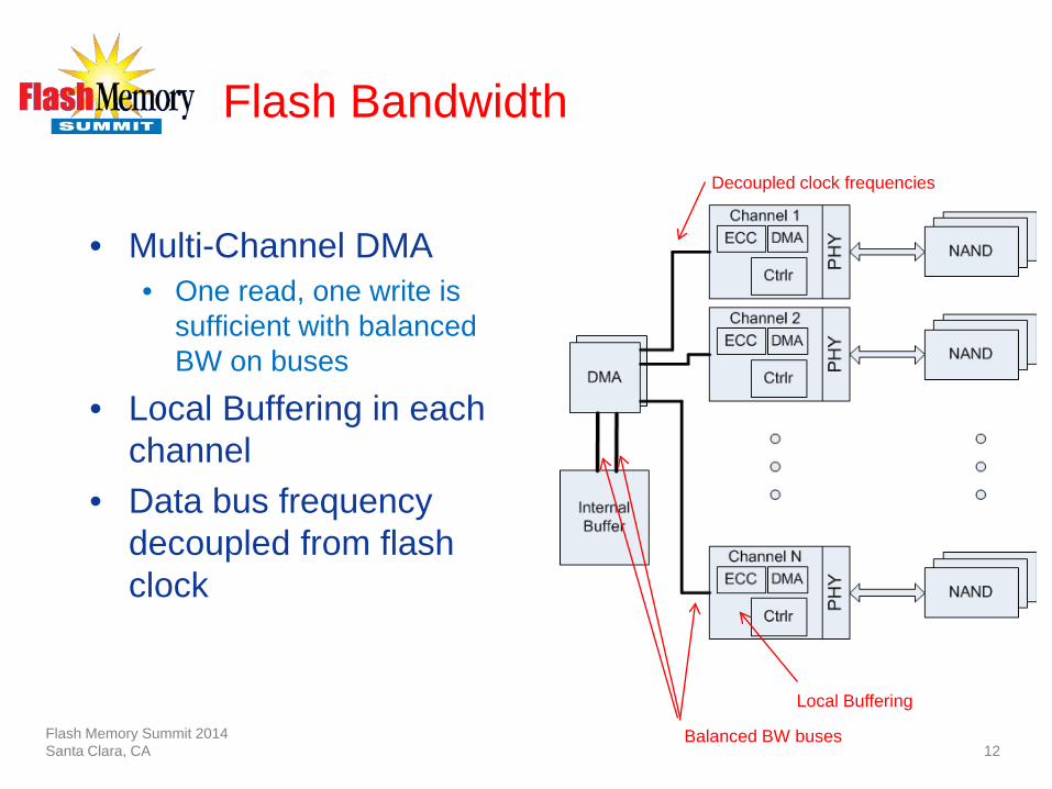
Flash Bandwidth
• Multi-Channel DMA • One read, one write is
sufficient with balanced BW on buses
• Local Buffering in each channel
• Data bus frequency decoupled from flash clock
Flash Memory Summit 2014 Santa Clara, CA
12
Local Buffering
Balanced BW buses
Decoupled clock frequencies
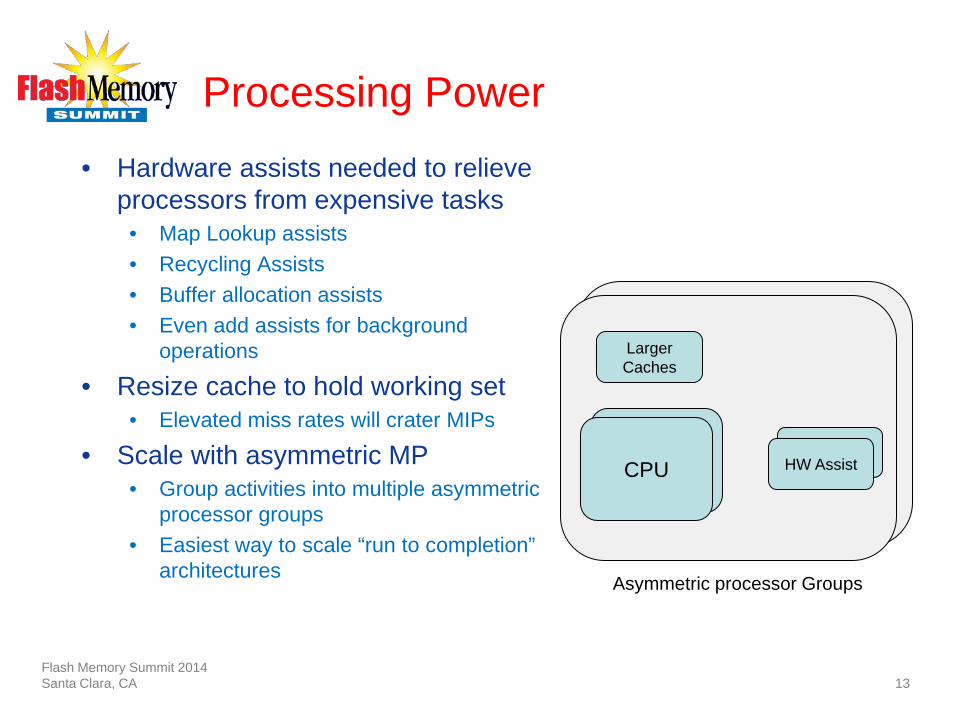
Processing Power • Hardware assists needed to relieve
processors from expensive tasks • Map Lookup assists • Recycling Assists • Buffer allocation assists • Even add assists for background
operations
• Resize cache to hold working set • Elevated miss rates will crater MIPs
• Scale with asymmetric MP • Group activities into multiple asymmetric
processor groups • Easiest way to scale “run to completion”
architectures
Flash Memory Summit 2014 Santa Clara, CA
13
CPU
Larger Caches
Map Lookup Assist HW Assist
Asymmetric processor Groups

Adding up all the Architectural Changes
Flash Memory Summit 2014 Santa Clara, CA
14
• When you sum up the required architectural changes…
• You realize that you practically have to throw your old SATA architecture out and start from scratch
FTL Impacts
• Bounding recovery Time requires new FTL techniques • Journaling FTL is essential to manage flush rates
and to bound the recovery interval. • High IOPs need FTL HW assists
• Map lookups • Recycling • Extensible structures for Storing and Managing
Hints
Flash Memory Summit 2014 Santa Clara, CA
15
Firmware Impacts
• More commands in flight • More resources required to track/manage commands • Algorithmic changes – sub-scalar algorithms don’t show up at low
IOPs (data coherency, searches, etc) • Scheduling becomes more challenging to keep the pipe full • Minimizing Tenure is critical
• Flash scheduling considerations • Same amount of flash as SATA SSD, but substantially more IOPs • On chip buffering requires more robust resource management • Requires entire scheduling layer redesign
• Background task management • Shorten background task segments. On “run to completion”
architectures
Flash Memory Summit 2014 Santa Clara, CA
16

Flash Memory Summit 2014 Santa Clara, CA
17
Questions?


![JEDEC JC-64.8 SSD Standards [Compatibility Mode].pdfSSD Definition ‣A solid state drive (SSD) is a non-volatile storage device. A controller is included in the device with one or](https://img.pdfslide.us/doc/110x75/5f04b07e7e708231d40f37a9/jedec-jc-648-ssd-standards-compatibility-modepdf-ssd-definition-aa-solid-state.jpg)