Embed Size (px)
Citation preview

http://www.njr.com/
Designated client product
This product will be discontinued its production in the near term. And it is provided for customers currently in use only, with a time limit. It can not be available for your new project. Please select other new or
existing products. For more information, please contact our sales office in your region.
New Japan Radio Co.,Ltd.
Ver.02
NJW1301
- 1 -
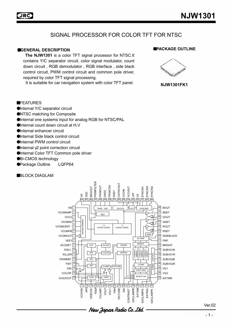
SIGNAL PROCESSOR FOR COLOR TFT FOR NTSC
PACKAGE OUTLINE
FEATURES Internal Y/C separator circuit NTSC matching for Composite Internal one systems input for analog RGB for NTSC/PAL Internal count down circuit at H,V Internal enhancer circuit Internal Side black control circuit Internal PWM control circuit Internal γ2 point correction circuit Internal Color TFT Common pole driver Bi-CMOS technology Package Outline LQFP64 BLOCK DIAGLAM
NJW1301FK1
GENERAL DESCRIPTION The NJW1301 is a color TFT signal processor for NTSC.It contains Y/C separator circuit, color signal modulator, count down circuit , RGB demodulator , RGB interface , side black control circuit, PWM control circuit and common pole driver, required by color TFT signal processing.
It is suitable for car navigation system with color TFT panel.
VCOMCENT
VC
XO
IN
AP
C
VID
EO
IN
TR
AP
YC
LAM
P
YO
UT
VC
C1
YIN
H
PIC
TU
RE
SW
CO
NT
RA
ST
GA
CLA
MP
B
EX
TIN
B
GA
CLA
MP
G
EX
TIN
G
GA
CLA
MP
R
VD
VD
D
RE
GO
UT
VC
OIN
PW
MF
ILT
ER
PW
MO
UT
GN
D2
PW
MC
ON
GN
D1
CS
YN
CO
UT
VC
OO
UT
LPF
VS
SY
NC
IN1
SY
NC
SW
SY
NC
IN2
VCXOOUT
COLOR
CIN
TINT
PWMREF
KILLER
FADJ
ACCDET
VEE1
VCOMOUT
VCOMFB
VCOMIN
VCC3
VCOMAMP
HD
EXTINR
VG2
VG1
SUBVG2R
SUBVG2B
SUBVG1R
SUBVG1B
BRIGHT
FRP
SIDEBLACK
RDET
ROUT
GDET
GOUT
BDET
BOUT 1
2
3
4
5
6
7
8
9
10
11
12
13
14
15
16
49 50 51 52 53 54 55 56 57 58 59 60 61 62 63 64
32 31 30 29 28 27 26 25 24 23 22 21 20 19 18 17
48
47
46
45
44
43
42
41
40
39
38
37
36
35
34
33
VREF
AFC SYNCSEP PWM OSC
H COUNT DOWN
CO
MM
ON
DR
IVE
R
ACC
TINT
VCXO
HPF
KILLER
APC
MATRIX COLOR
DEMOD
PICTURE
TRAP
CLAMP
REG
GA
MM
A
CO
RR
EC
T
32fHVCO
V COUNT DOWN
GA
MM
A
CO
RR
EC
T
GA
MM
A
CO
RR
EC
T
CONT RAST
BRIGHT
INT/EXT SW
CLAMP
ALTAMP
GA
MM
A
CO
NT
RO
L

Ver.02
NJW1301
- 2 -
ABSOLUTE MAXIMUM RATINGS (Ta=25°°°°C)
PARAMETERS SYMBOL RATINGS UNIT
Supply Voltage 1 VCC1-GND1 8.0 V
Supply Voltage 2 VCC3-VEE1 15.0 V
Supply Voltage 3 VDD-GND1 7.0 V
Supply Voltage 4 VEE1-GND1 -7.0 V
Power Dissipation PD 700 mW
Each Adjustment Terminal VIN VCC1 V
SYNC OUT Voltage VSD VEE1+15.0 V
Picture Input Voltage VVDIN 3.0 VP-P
External Input Voltage EXTIN VCC1 V
FRP Input Signal Voltage FRPIN VCC1 V
SYNC Input Voltage SYNCIN VCC1 V
Analog RGB Input Signal RGBIN 3.0 VPP
Operating Temperature Range Topr -30 to +85 °C
Storage Temperature Range Tstg -40 to +125 °C
Ver.02
NJW1301
- 3 -
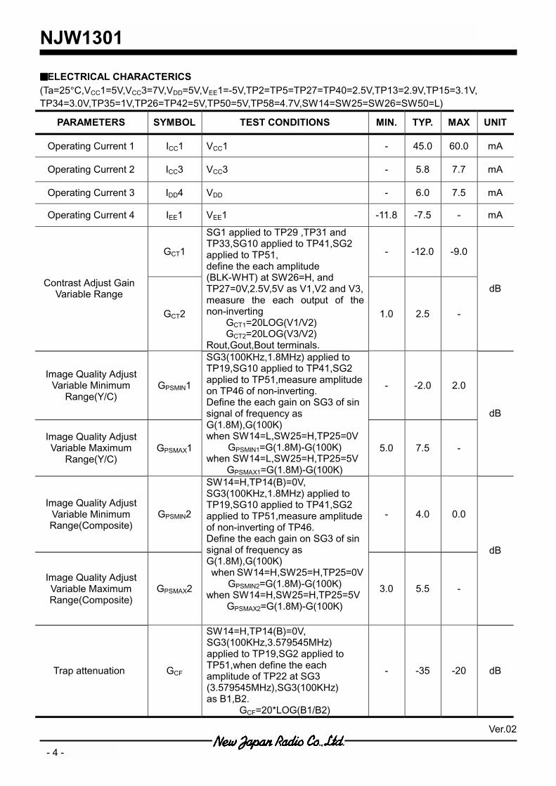
RECOMMENDED OPERATING CONDITION (Ta=25°°°°C)
PARAMETER SYMBOL TEST CONDITION MIN. TYP. MAX. UNIT
- VCC1-GND 4.75 5.00 5.25 V
- VCC3-VEE1 11.00 12.00 13.00 V
- VEE1-GND1 -5.25 -5.0 -4.75 V Supply Voltage Range
- VDD-GND1 4.75 5.00 5.25 V
Y Input Signal Voltage YIN Pedestal-White 0.30 0.35 0.40 VP-P
C Input Signal Voltage CIN Amplitude of Burst Signal 0.10 0.15 0.20 VP-P
Analog RGB Input Signal RGBIN 0.6 0.7 0.8 VP-P
SYNC Input Signal SYNCIN 0.3 1.0 1.5 VP-P
Gamma 1 Adjust Voltage VG1 1.5 - 3.5 V
Gamma 2 Adjust Voltage VG2 1.5 - 3.8 V
Bright Adjust Voltage BRIGHT 1.8 - 3.4 V
PWM Control Voltage PWMCONT 0 - 5 V
(Point 1) When suspected SYNC input to NJW1301, necessary on 5H(1H:horizontal term ,about 63.5us) of pulth width of suspected SYNC.
(Point 2) Investigation Crosstalk level when design for depend to application. (Point 3) Do not input the intermediate step signal at External terminal to use OSD signal for EXTRGB.
The EXRRGB accept only white(0.7V,white 100%) – black(0V)signal.
Ver.02
NJW1301
- 4 -
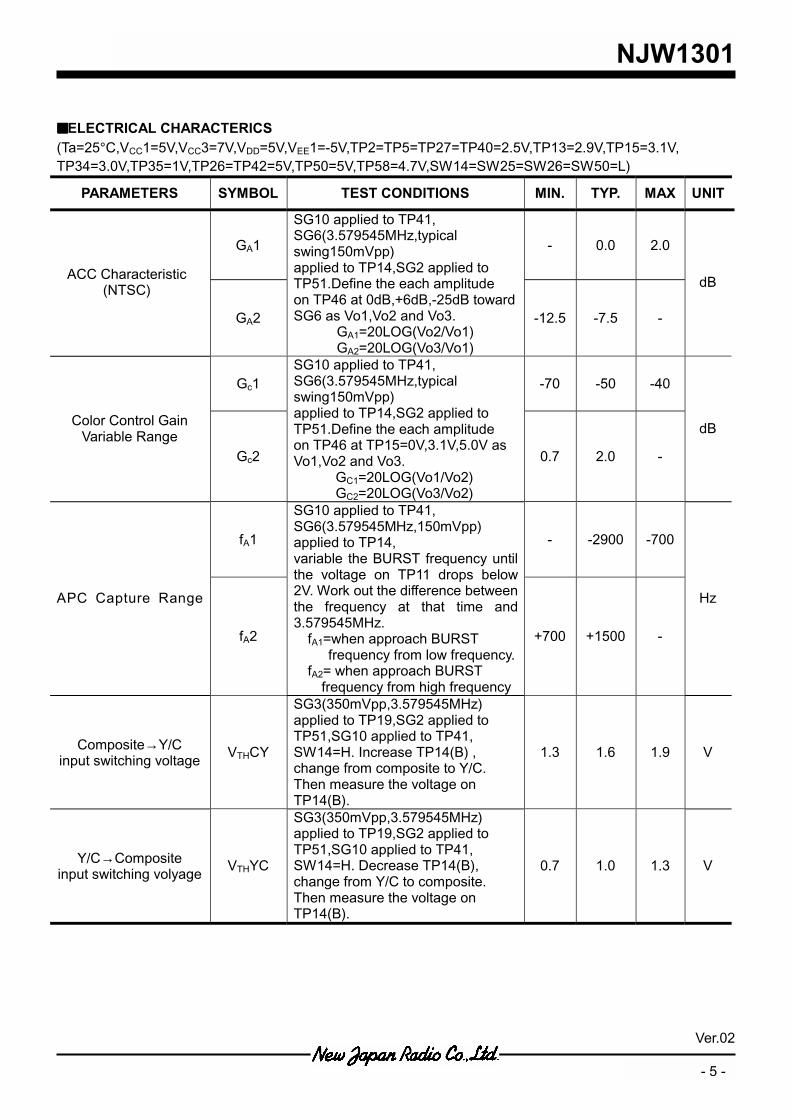
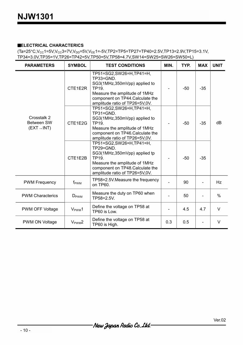
ELECTRICAL CHARACTERICS (Ta=25°C,VCC1=5V,VCC3=7V,VDD=5V,VEE1=-5V,TP2=TP5=TP27=TP40=2.5V,TP13=2.9V,TP15=3.1V, TP34=3.0V,TP35=1V,TP26=TP42=5V,TP50=5V,TP58=4.7V,SW14=SW25=SW26=SW50=L)
PARAMETERS SYMBOL TEST CONDITIONS MIN. TYP. MAX UNIT
Operating Current 1 ICC1 VCC1 - 45.0 60.0 mA
Operating Current 2 ICC3 VCC3 - 5.8 7.7 mA
Operating Current 3 IDD4 VDD - 6.0 7.5 mA
Operating Current 4 IEE1 VEE1 -11.8 -7.5 - mA
GCT1 - -12.0 -9.0
Contrast Adjust Gain Variable Range
GCT2
SG1 applied to TP29 ,TP31 and TP33,SG10 applied to TP41,SG2 applied to TP51, define the each amplitude (BLK-WHT) at SW26=H, and TP27=0V,2.5V,5V as V1,V2 and V3, measure the each output of the non-inverting
GCT1=20LOG(V1/V2) GCT2=20LOG(V3/V2)
Rout,Gout,Bout terminals.
1.0 2.5 -
dB
Image Quality Adjust Variable Minimum
Range(Y/C) GPSMIN1 - -2.0 2.0
Image Quality Adjust Variable Maximum
Range(Y/C) GPSMAX1
SG3(100KHz,1.8MHz) applied to TP19,SG10 applied to TP41,SG2 applied to TP51,measure amplitude on TP46 of non-inverting. Define the each gain on SG3 of sin signal of frequency as G(1.8M),G(100K) when SW14=L,SW25=H,TP25=0V
GPSMIN1=G(1.8M)-G(100K) when SW14=L,SW25=H,TP25=5V
GPSMAX1=G(1.8M)-G(100K)
5.0 7.5 -
dB
Image Quality Adjust Variable Minimum Range(Composite)
GPSMIN2 - 4.0 0.0
Image Quality Adjust Variable Maximum Range(Composite)
GPSMAX2
SW14=H,TP14(B)=0V, SG3(100KHz,1.8MHz) applied to TP19,SG10 applied to TP41,SG2 applied to TP51,measure amplitude of non-inverting of TP46. Define the each gain on SG3 of sin signal of frequency as G(1.8M),G(100K) when SW14=H,SW25=H,TP25=0V
GPSMIN2=G(1.8M)-G(100K) when SW14=H,SW25=H,TP25=5V
GPSMAX2=G(1.8M)-G(100K)
3.0 5.5 -
dB
Trap attenuation GCF
SW14=H,TP14(B)=0V, SG3(100KHz,3.579545MHz) applied to TP19,SG2 applied to TP51,when define the each amplitude of TP22 at SG3 (3.579545MHz),SG3(100KHz) as B1,B2.
GCF=20*LOG(B1/B2)
- -35 -20 dB
Ver.02
NJW1301
- 5 -
ELECTRICAL CHARACTERICS (Ta=25°C,VCC1=5V,VCC3=7V,VDD=5V,VEE1=-5V,TP2=TP5=TP27=TP40=2.5V,TP13=2.9V,TP15=3.1V, TP34=3.0V,TP35=1V,TP26=TP42=5V,TP50=5V,TP58=4.7V,SW14=SW25=SW26=SW50=L)
PARAMETERS SYMBOL TEST CONDITIONS MIN. TYP. MAX UNIT
GA1 - 0.0 2.0
ACC Characteristic (NTSC)
GA2
SG10 applied to TP41, SG6(3.579545MHz,typical swing150mVpp) applied to TP14,SG2 applied to TP51.Define the each amplitude on TP46 at 0dB,+6dB,-25dB toward SG6 as Vo1,Vo2 and Vo3.
GA1=20LOG(Vo2/Vo1) GA2=20LOG(Vo3/Vo1)
-12.5 -7.5 -
dB
Gc1 -70 -50 -40
Color Control Gain Variable Range
Gc2
SG10 applied to TP41, SG6(3.579545MHz,typical swing150mVpp) applied to TP14,SG2 applied to TP51.Define the each amplitude on TP46 at TP15=0V,3.1V,5.0V as Vo1,Vo2 and Vo3.
GC1=20LOG(Vo1/Vo2) GC2=20LOG(Vo3/Vo2)
0.7 2.0 -
dB
fA1 - -2900 -700
APC Capture Range
fA2
SG10 applied to TP41, SG6(3.579545MHz,150mVpp) applied to TP14, variable the BURST frequency until the voltage on TP11 drops below 2V. Work out the difference between the frequency at that time and 3.579545MHz.
fA1=when approach BURST frequency from low frequency. fA2= when approach BURST
frequency from high frequency
+700 +1500 -
Hz
Composite→Y/C input switching voltage
VTHCY
SG3(350mVpp,3.579545MHz) applied to TP19,SG2 applied to TP51,SG10 applied to TP41, SW14=H. Increase TP14(B) , change from composite to Y/C. Then measure the voltage on TP14(B).
1.3 1.6 1.9 V
Y/C→Composite input switching volyage
VTHYC
SG3(350mVpp,3.579545MHz) applied to TP19,SG2 applied to TP51,SG10 applied to TP41, SW14=H. Decrease TP14(B), change from Y/C to composite. Then measure the voltage on TP14(B).
0.7 1.0 1.3 V
Ver.02
NJW1301
- 6 -
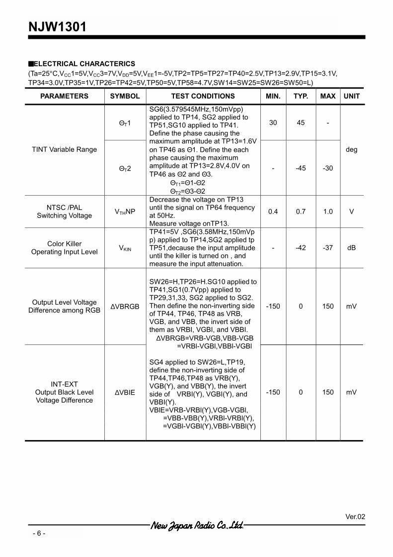
ELECTRICAL CHARACTERICS (Ta=25°C,VCC1=5V,VCC3=7V,VDD=5V,VEE1=-5V,TP2=TP5=TP27=TP40=2.5V,TP13=2.9V,TP15=3.1V, TP34=3.0V,TP35=1V,TP26=TP42=5V,TP50=5V,TP58=4.7V,SW14=SW25=SW26=SW50=L)
PARAMETERS SYMBOL TEST CONDITIONS MIN. TYP. MAX UNIT
ΘT1 30 45 -
TINT Variable Range
ΘT2
SG6(3.579545MHz,150mVpp) applied to TP14, SG2 applied to TP51,SG10 applied to TP41. Define the phase causing the maximum amplitude at TP13=1.6V on TP46 as Θ1. Define the each phase causing the maximum amplitude at TP13=2.8V,4.0V on TP46 as Θ2 and Θ3.
ΘT1=Θ1-Θ2 ΘT2=Θ3-Θ2
- -45 -30
deg
NTSC /PAL Switching Voltage VTHNP
Decrease the voltage on TP13 until the signal on TP64 frequency at 50Hz. Measure voltage onTP13.
0.4 0.7 1.0 V
Color Killer Operating Input Level VKIN
TP41=5V ,SG6(3.58MHz,150mVpp) applied to TP14,SG2 applied tp TP51,decause the input amplitude until the killer is turned on , and measure the input attenuation.
- -42 -37 dB
Output Level Voltage Difference among RGB ∆VBRGB -150 0 150 mV
INT-EXT Output Black Level Voltage Difference
∆VBIE
SW26=H,TP26=H.SG10 applied to TP41,SG1(0.7Vpp) applied to TP29,31,33, SG2 applied to SG2. Then define the non-inverting side of TP44, TP46, TP48 as VRB, VGB, and VBB, the invert side of them as VRBI, VGBI, and VBBI.
∆VBRGB=VRB-VGB,VBB-VGB =VRBl-VGBl,VBBl-VGBl
SG4 applied to SW26=L,TP19, define the non-inverting side of TP44,TP46,TP48 as VRB(Y), VGB(Y), and VBB(Y), the invert side of VRBI(Y), VGBI(Y), and VBBI(Y). VBlE=VRB-VRBl(Y),VGB-VGBl,
=VBB-VBB(Y),VRBl-VRBl(Y), =VGBl-VGBl(Y),VBBl-VBBl(Y)
-150 0 150 mV
Ver.02
NJW1301
- 7 -
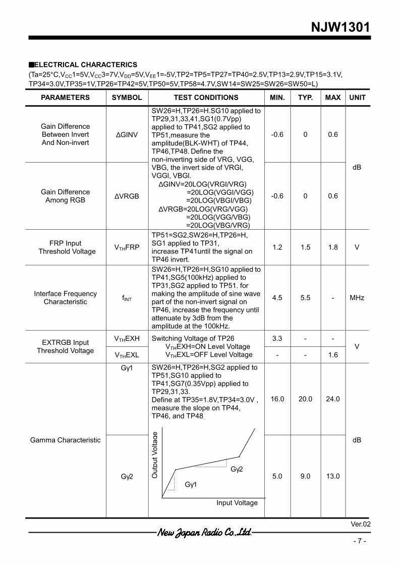
ELECTRICAL CHARACTERICS (Ta=25°C,VCC1=5V,VCC3=7V,VDD=5V,VEE1=-5V,TP2=TP5=TP27=TP40=2.5V,TP13=2.9V,TP15=3.1V, TP34=3.0V,TP35=1V,TP26=TP42=5V,TP50=5V,TP58=4.7V,SW14=SW25=SW26=SW50=L)
PARAMETERS SYMBOL TEST CONDITIONS MIN. TYP. MAX UNIT
Gain Difference Between Invert And Non-invert
∆GINV -0.6 0 0.6
Gain Difference Among RGB ∆VRGB
SW26=H,TP26=H.SG10 applied to TP29,31,33,41,SG1(0.7Vpp) applied to TP41,SG2 applied to TP51,measure the amplitude(BLK-WHT) of TP44, TP46,TP48. Define the non-inverting side of VRG, VGG, VBG, the invert side of VRGl, VGGl, VBGl.
∆GINV=20LOG(VRGI/VRG) =20LOG(VGGI/VGG)
=20LOG(VBGI/VBG) ∆VRGB=20LOG(VRG/VGG)
=20LOG(VGG/VBG) =20LOG(VBG/VRG)
-0.6 0 0.6
dB
FRP Input Threshold Voltage VTHFRP
TP51=SG2,SW26=H,TP26=H, SG1 applied to TP31, increase TP41until the signal on TP46 invert.
1.2 1.5 1.8 V
Interface Frequency Characteristic fINT
SW26=H,TP26=H,SG10 applied to TP41,SG5(100kHz) applied to TP31,SG2 applied to TP51. for making the amplitude of sine wave part of the non-invert signal on TP46, increase the frequency until attenuate by 3dB from the amplitude at the 100kHz.
4.5 5.5 - MHz
VTHEXH 3.3 - - EXTRGB Input Threshold Voltage
VTHEXL
Switching Voltage of TP26 VTHEXH=ON Level Voltage VTHEXL=OFF Level Voltage - - 1.6
V
Gγ1
16.0 20.0 24.0
Gamma Characteristic
Gγ2
SW26=H,TP26=H,SG2 applied to TP51,SG10 applied to TP41,SG7(0.35Vpp) applied to TP29,31,33. Define at TP35=1.8V,TP34=3.0V , measure the slope on TP44, TP46, and TP48.
5.0 9.0 13.0
dB
Gγ2
Gγ1
Input Voltage
Out
put V
olta
ge
Ver.02
NJW1301
- 8 -
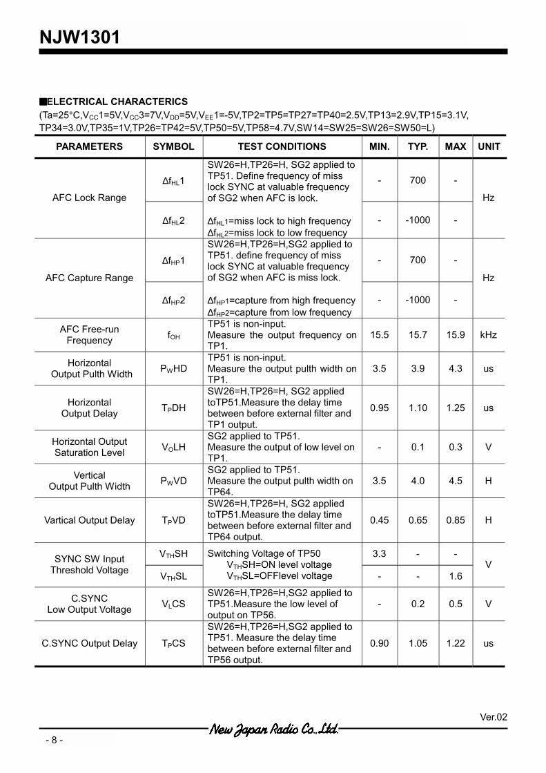
ELECTRICAL CHARACTERICS (Ta=25°C,VCC1=5V,VCC3=7V,VDD=5V,VEE1=-5V,TP2=TP5=TP27=TP40=2.5V,TP13=2.9V,TP15=3.1V, TP34=3.0V,TP35=1V,TP26=TP42=5V,TP50=5V,TP58=4.7V,SW14=SW25=SW26=SW50=L)
PARAMETERS SYMBOL TEST CONDITIONS MIN. TYP. MAX UNIT
∆fHL1 - 700 -
AFC Lock Range
∆fHL2
SW26=H,TP26=H, SG2 applied to TP51. Define frequency of miss lock SYNC at valuable frequency of SG2 when AFC is lock. ∆fHL1=miss lock to high frequency ∆fHL2=miss lock to low frequency
- -1000 -
Hz
∆fHP1 - 700 -
AFC Capture Range
∆fHP2
SW26=H,TP26=H,SG2 applied to TP51. define frequency of miss lock SYNC at valuable frequency of SG2 when AFC is miss lock. ∆fHP1=capture from high frequency ∆fHP2=capture from low frequency
- -1000 -
Hz
AFC Free-run Frequency fOH
TP51 is non-input. Measure the output frequency on TP1.
15.5 15.7 15.9 kHz
Horizontal Output Pulth Width PWHD
TP51 is non-input. Measure the output pulth width on TP1.
3.5 3.9 4.3 us
Horizontal Output Delay TPDH
SW26=H,TP26=H, SG2 applied toTP51.Measure the delay time between before external filter and TP1 output.
0.95 1.10 1.25 us
Horizontal Output Saturation Level VOLH
SG2 applied to TP51. Measure the output of low level on TP1.
- 0.1 0.3 V
Vertical Output Pulth Width PWVD
SG2 applied to TP51. Measure the output pulth width on TP64.
3.5 4.0 4.5 H
Vartical Output Delay TPVD
SW26=H,TP26=H, SG2 applied toTP51.Measure the delay time between before external filter and TP64 output.
0.45 0.65 0.85 H
VTHSH 3.3 - - SYNC SW Input Threshold Voltage
VTHSL
Switching Voltage of TP50 VTHSH=ON level voltage VTHSL=OFFlevel voltage - - 1.6
V
C.SYNC Low Output Voltage VLCS
SW26=H,TP26=H,SG2 applied to TP51.Measure the low level of output on TP56.
- 0.2 0.5 V
C.SYNC Output Delay TPCS
SW26=H,TP26=H,SG2 applied to TP51. Measure the delay time between before external filter and TP56 output.
0.90 1.05 1.22 us
Ver.02
NJW1301
- 9 -
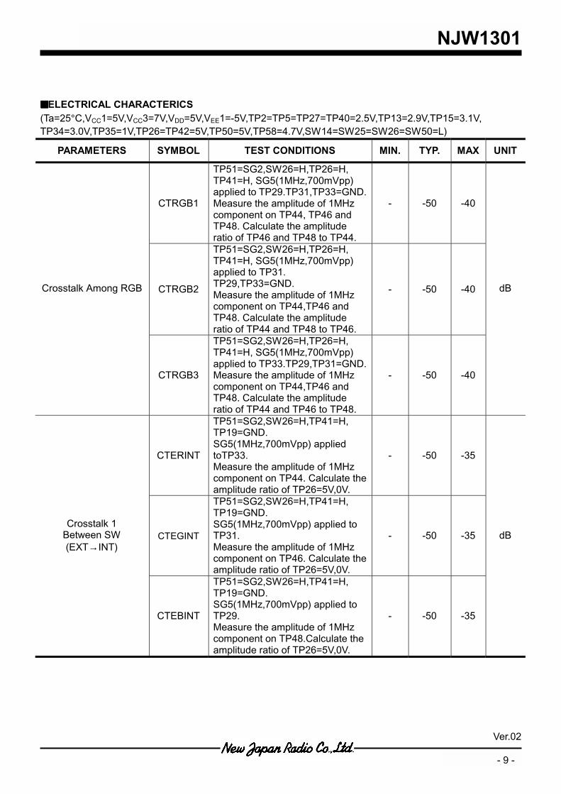
ELECTRICAL CHARACTERICS (Ta=25°C,VCC1=5V,VCC3=7V,VDD=5V,VEE1=-5V,TP2=TP5=TP27=TP40=2.5V,TP13=2.9V,TP15=3.1V, TP34=3.0V,TP35=1V,TP26=TP42=5V,TP50=5V,TP58=4.7V,SW14=SW25=SW26=SW50=L)
PARAMETERS SYMBOL TEST CONDITIONS MIN. TYP. MAX UNIT
CTRGB1
TP51=SG2,SW26=H,TP26=H, TP41=H, SG5(1MHz,700mVpp) applied to TP29.TP31,TP33=GND. Measure the amplitude of 1MHz component on TP44, TP46 and TP48. Calculate the amplitude ratio of TP46 and TP48 to TP44.
- -50 -40
CTRGB2
TP51=SG2,SW26=H,TP26=H, TP41=H, SG5(1MHz,700mVpp) applied to TP31. TP29,TP33=GND. Measure the amplitude of 1MHz component on TP44,TP46 and TP48. Calculate the amplitude ratio of TP44 and TP48 to TP46.
- -50 -40 Crosstalk Among RGB
CTRGB3
TP51=SG2,SW26=H,TP26=H, TP41=H, SG5(1MHz,700mVpp) applied to TP33.TP29,TP31=GND. Measure the amplitude of 1MHz component on TP44,TP46 and TP48. Calculate the amplitude ratio of TP44 and TP46 to TP48.
- -50 -40
dB
CTERINT
TP51=SG2,SW26=H,TP41=H, TP19=GND. SG5(1MHz,700mVpp) applied toTP33. Measure the amplitude of 1MHz component on TP44. Calculate the amplitude ratio of TP26=5V,0V.
- -50 -35
CTEGINT
TP51=SG2,SW26=H,TP41=H, TP19=GND. SG5(1MHz,700mVpp) applied to TP31. Measure the amplitude of 1MHz component on TP46. Calculate the amplitude ratio of TP26=5V,0V.
- -50 -35 Crosstalk 1
Between SW (EXT→INT)
CTEBINT
TP51=SG2,SW26=H,TP41=H, TP19=GND. SG5(1MHz,700mVpp) applied to TP29. Measure the amplitude of 1MHz component on TP48.Calculate the amplitude ratio of TP26=5V,0V.
- -50 -35
dB
Ver.02
NJW1301
- 10 -
ELECTRICAL CHARACTERICS (Ta=25°C,VCC1=5V,VCC3=7V,VDD=5V,VEE1=-5V,TP2=TP5=TP27=TP40=2.5V,TP13=2.9V,TP15=3.1V, TP34=3.0V,TP35=1V,TP26=TP42=5V,TP50=5V,TP58=4.7V,SW14=SW25=SW26=SW50=L)
PARAMETERS SYMBOL TEST CONDITIONS MIN. TYP. MAX UNIT
CTE1E2R
TP51=SG2,SW26=H,TP41=H, TP33=GND. SG3(1MHz,350mVpp) applied to TP19. Measure the amplitude of 1MHz component on TP44.Calculate the amplitude ratio of TP26=5V,0V.
- -50 -35
CTE1E2G
TP51=SG2,SW26=H,TP41=H, TP31=GND. SG3(1MHz,350mVpp) applied to TP19. Measure the amplitude of 1MHz component on TP46.Calculate the amplitude ratio of TP26=5V,0V.
- -50 -35 Crosstalk 2
Between SW (EXT→INT)
CTE1E2B
TP51=SG2,SW26=H,TP41=H, TP29=GND. SG3(1MHz,350mVpp) applied tp TP19. Measure the amplitude of 1MHz component on TP48.Calculate the amplitude ratio of TP26=5V,0V.
- -50 -35
dB
PWM Frequency fPWM TP58=2.5V.Measure the frequency on TP60. - 90 - Hz
PWM Characterics DPWM Measure the duty on TP60 when TP58=2.5V. - 50 - %
PWM OFF Voltage VPWM1 Define the voltage on TP58 at TP60 is Low. - 4.5 4.7 V
PWM ON Voltage VPWM2 Define the voltage on TP58 at TP60 is High. 0.3 0.5 - V

Ver.02
NJW1301
- 11 -
ELECTRICAL CHARACTERICS (Ta=25°C,VCC1=5V,VCC3=7V,VDD=5V,VEE1=-5V,TP2=TP5=TP27=TP40=2.5V,TP13=2.9V,TP15=3.1V, TP34=3.0V,TP35=1V,TP26=TP42=5V,TP50=5V,TP58=4.7V,SW14=SW25=SW26=SW50=L)
PARAMETERS SYMBOL TEST CONDITIONS MIN. TYP. MAX UNIT
Side-black Level VSB
TP41=SG10,TP51=SG2. When TP42=5V ,define the non-invertiing black level of TP44, TP46,TP48 as VRB,VGB,VBB. When TP42=5V ,define the invertiing black level of TP44,TP46,TP48 as VRBI,VGBI,VBBI. When TP42=0V ,define the non-invertiing black level of TP44, TP46,TP48 asVRB(B),VGB(B), VBB(B). When TP42=0V ,define the invertiing black level of TP44,TP46,TP48 as VRBI(B),VGBI(B),VBBI(B). VdBLACK=VRB-VRB(B),
VGB-VGB(B), VBB-VBB(B)
=VRBI(B)-VRBI, VGBI(B)-VGBI, VBBI(B)-VBBI
- 500 - mV
VCOM Output Slew Rate SRVCOM
SG9 applied toTP4. Measure the tern on and tern off time at 20% to 80% on TP6 output wave. Then convert to slew rate.
4.0 9.0 - V/us
VCOM Center Voltage VCVCOM SG9 applied to TP4. Measure the center voltage of TP6 output voltage.
0.9 1.2 1.5 V
VCOM Amplitude VAVCOM SG9 applied to TP4. Measure the output ampukitude on TP6.
6.0 6.5 7.0 VP-P
Delay Between Y-C ∆TdYC - 0 - ns
RGB Slew Rate SRRGB
TP29,TP31,TP33=SG8,TP41=SG10,TP51=SG2. Measure the tern on and tern off time at 20% to 80% of output wave on TP44,TP46,TP48. Then convert to slew rate.
9 22 40 V/us
Ver.02
NJW1301
- 12 -
ELECTRICAL CHARACTERICS (Ta=25°C,VCC1=5V,VCC3=7V,VDD=5V,VEE1=-5V,TP2=TP5=TP27=TP40=2.5V,TP13=2.9V,TP15=3.1V, TP34=3.0V,TP35=1V,TP26=TP42=5V,TP50=5V,TP58=4.7V,SW14=SW25=SW26=SW50=L)
PARAMETERS SYMBOL TEST CONDITIONS MIN. TYP. MAX UNIT
Demodulation Relativity Ampulitude
(R-Y/B-Y)
R-Y B-Y - 0.65 -
Demodulation Relativity Ampulitude
(G-Y/B-Y)
G-Y B-Y
SG10 applied to TP41, SG6(3.58MHz,150mVpp) applied to TP41,SG2 applied to TP51,TP14 applied to TP51. TP34=3.0V,TP35=1.5V,vary the chroma phase on SG6, define non-inverting maximum output amplitude of TP44,TP46,TP48 as VR,VG,VB.
(R-Y)/(B-Y)=VR/VB (G-Y)/(B-Y)=VG/VB
- 0.45 -
-
Demodulation Relativity Phase
(R-Y/B-Y) ΘRB - 105 -
Demodulation Relativity Phase
(G-Y/B-Y) ΘGB
SG10 applied to TP41, SG6(3.58MHz,150mVpp) applied to TP14,SG2 applied to TP51, TP34=3.0V,TP35=1.5V,vary the chroma phase on SG6,define tne phase at maximum output amplitude of TP44,TP46,TP48 as ΘR,ΘG,ΘB.
ΘRB=ΘR-ΘB ΘGB=ΘG-ΘB
- 240 -
deg
Demodulation Output residual Carrier VCR
TP41=5V, SG6(3.58MHz,150mVpp) applied to TP14,SG2 applied to TP51,adjust the chroma phase on SG6 for maximum the amplitude of TP48.Measure the ratio of 7.159059MHz component to the 15.734kHz component.
- 40 - dB
Horizontal AFC Keep Limit Input VINPM
SW26=H,TP26=H,TP51=SG2. define the amplitude of miss lock SYNC at decrease amplituide of SG2 when AFC is miss lock.
- 15 28 mV
NJW1301
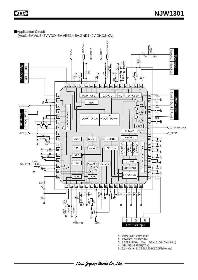
Application Circuit
(Vcc1=5V,Vcc3=7V,VDD=5V,VEE1=-5V,GND1=0V,GND2=0V)
1 : 2SC2120Y, 2SC1959Y 2 : 2SA950Y, 2SA562TM 3 : 3.579545MHz X’tal DSX151GA(Daishinku) 4 : NTL4532-S3R6B(TDK) 5 : 32fH Ceramic CSBLA503KECZF2(Murata)
1 2 3
4
5 6
7
8
9 10
11
12
13
14
15
16
49 5051 5253 54 55 56 5758 5960 61 62 63 64
32 3130 2928 27 26 25 2423 2221 20 19 18 17
48
47
46
45
44
43
42
41
40
39
38
37
36
35
34
33
1M
0.1u
0.01u
0.1u
Ext RGB InputB R G
VCC3
0.47u *2 *1
*3
3p
1000p
360
VCC1
GN
D1
Sync Output
VD
HD
O
utput Input
Com
mom
0.047
VEE1
300
4700p
*5
2K
12K
*40.1u
22P
1.2K
68u
0.01u
0.1u
0.1u
0.1u
0.1u
0.1u
1u
1u
1u
100
100
100
RG
B output Bout
Rout
Gout
1u+
2.2u4.7k
0.01u
+5KC
SYNC
OU
T
GN
D2
0.1u
Syncin2 SyncInput
Syncin1 910K
1u+
1.8K
5.6K +0.1u
8.2K
1u+
VIDEOIN
SIDEBLACK
FRP
VDD
PWM
OU
T
CONTRAST
GAM
MA
CO
NTR
OL
GAM
MA
CO
RR
ECT
GAM
MA
C
OR
REC
T
GAM
MA
C
OR
REC
T
BRIGHT
VREF
ALTAMP
AFC 32fHVCO SYNCSEP
V COUNT DOWN
H COUNT DOWN
CO
MM
ON
DR
IVER
ACC
TINT
VCXO
HPF
KILLER
INT/EXT SW
APC
MATRIX COLO
DEMOD
PICTURE
TRAP
CLAMP CLAMP
0.1uFCIN
REG
0.1u
PWM OSC
1u+
0.1u 5K
NJW1301
-14-
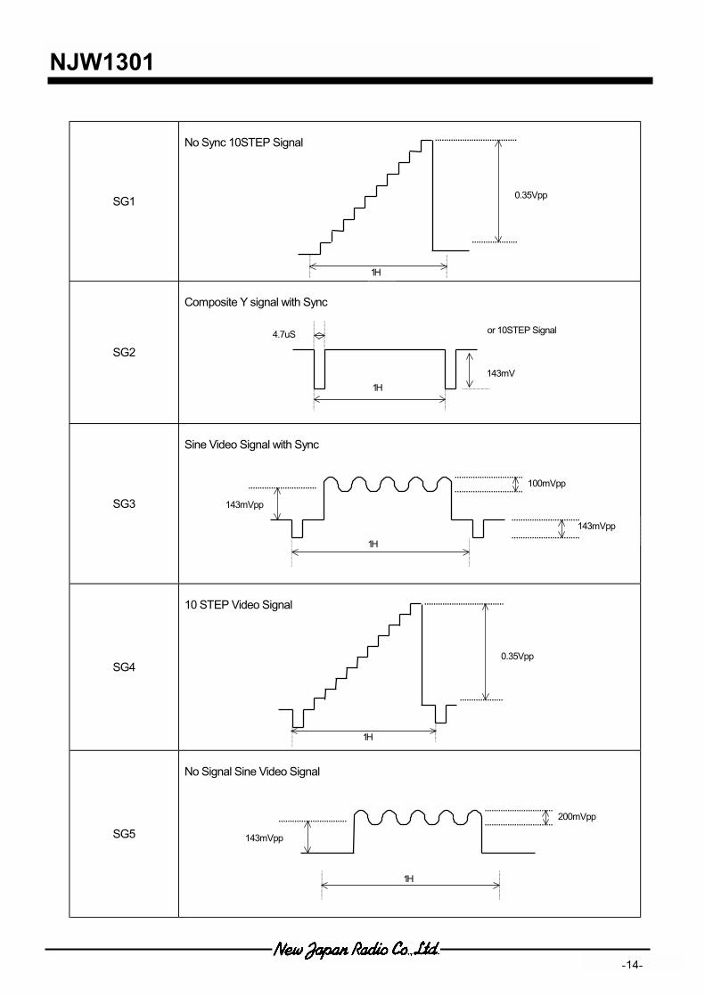
SG1
No Sync 10STEP Signal
SG2
Composite Y signal with Sync
SG3
Sine Video Signal with Sync
SG4
10 STEP Video Signal
SG5
No Signal Sine Video Signal
4.7uS
1H 143mV
0.35Vpp
143mVpp
100mVpp
143mVpp
1H
200mVpp
143mVpp
1H
or 10STEP Signal
1H
0.35Vpp
1H
NJW1301
-15-
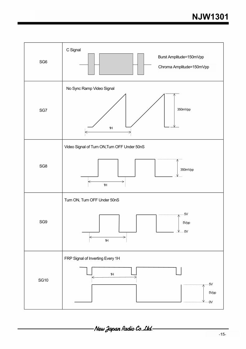
SG6
C Signal
SG7
No Sync Ramp Video Signal
SG8
Video Signal of Turn ON,Turn OFF Under 50nS
SG9
Turn ON, Turn OFF Under 50nS
SG10
FRP Signal of Inverting Every 1H
1H
350mVpp
350mVpp
1H
1H
5Vpp
0V
5V
1H
5Vpp
0V
5V
Chroma Amplitude=150mVpp
Burst Amplitude=150mVpp
NJW1301
-14-
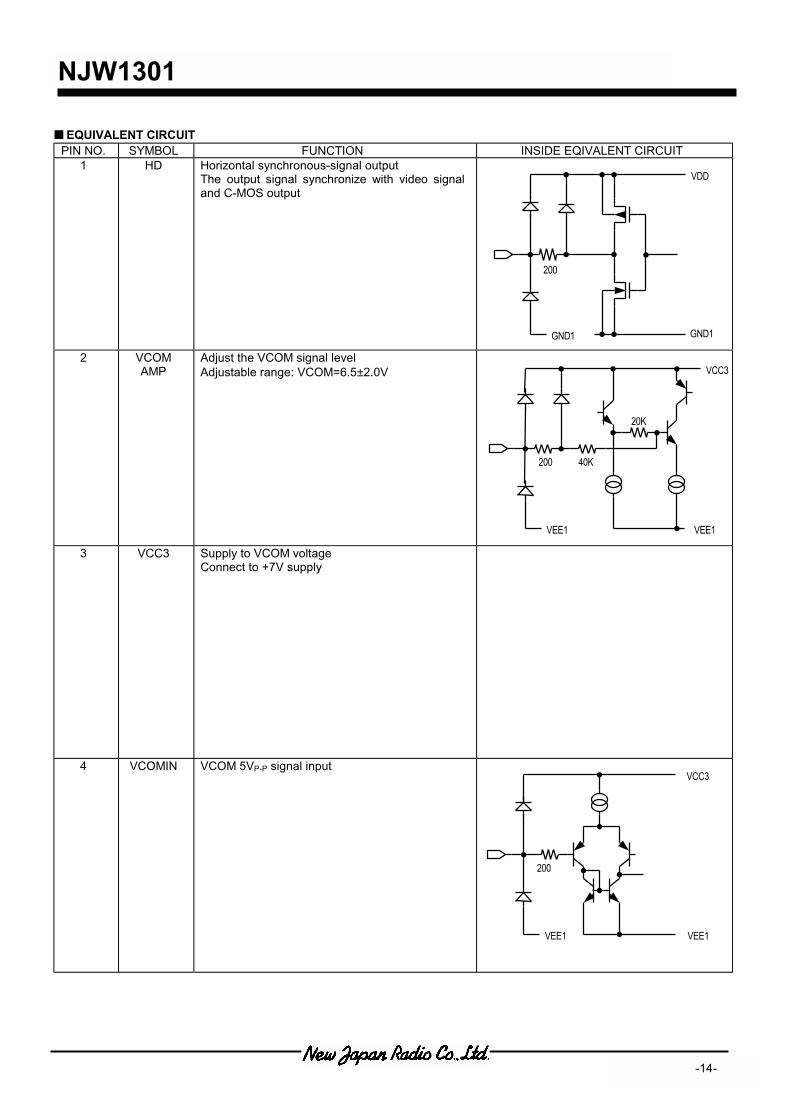
EQUIVALENT CIRCUIT PIN NO. SYMBOL FUNCTION INSIDE EQIVALENT CIRCUIT
1 HD Horizontal synchronous-signal output The output signal synchronize with video signal and C-MOS output
2 VCOM AMP
Adjust the VCOM signal level Adjustable range: VCOM=6.5±2.0V
3 VCC3 Supply to VCOM voltage Connect to +7V supply
4 VCOMIN VCOM 5VP-P signal input
200 40K
20K
VCC3
VEE1 VEE1
200
VCC3
VEE1 VEE1
VDD
GND1 GND1
200

NJW1301
-15-
EQUIVALENT CIRCUIT PIN NO. SYMBOL FUNCTION INSIDE EQIVALENT CIRCUIT
5 VCOM CENT
Adjust the center of VCOM voltage Adjustable range: VCOMCENT=1.2±1.5V
6 VCOMFB VCOM feedback signal Input the feedback signal (VCOMOUT) through the discrete transistor buffer
7 VCOM OUT
VCOM signal output Drive the common by connect discrete transistor
8 VEE1 Connect –5V supply at lowest voltage
36K
VCC3
VEE1 VEE1
100
VCC3
VEE1 VEE1
50K
200 75K
VCC3
VEE1 VEE1
NJW1301
-16-
EQUIVALENT CIRCUIT PIN NO. SYMBOL FUNCTION INSIDE EQIVALENT CIRCUIT
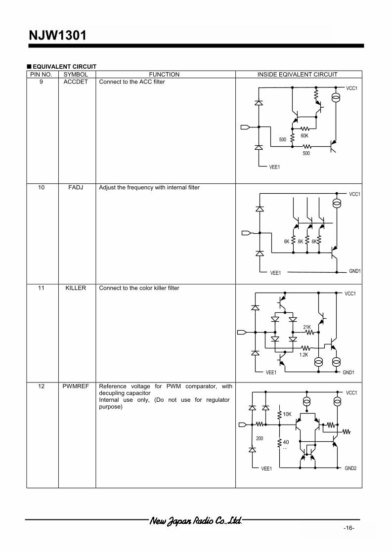
9 ACCDET Connect to the ACC filter
10 FADJ Adjust the frequency with internal filter
11 KILLER Connect to the color killer filter
12 PWMREF Reference voltage for PWM comparator, with decupling capacitor Internal use only, (Do not use for regulator purpose)
21K
1.2K
VCC1
VEE1 GND1
6K
VCC1
VEE1
6K 6K
GND1
500
60K 500
VCC1
VEE1
10K
200 40
K
VCC1
VEE1 GND2
NJW1301
-17-
EQUIVALENT CIRCUIT PIN NO. SYMBOL FUNCTION INSIDE EQIVALENT CIRCUIT
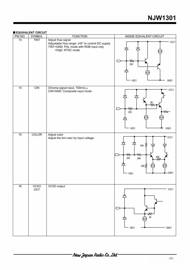
13 TINT Adjust Hue signal Adjustable Hue range: ±45° to control DC supply TINT=GND: PAL mode with RGB input only =High: NTSC mode
14 CIN Chroma signal input, 150mVP-P CIN=GND: Composite input mode
15 COLOR Adjust color Adjust the tint color by input voltage
16 VCXO OUT
VCXO output VCC1
VEE1 GND1
4K
200
5K
VCC1
VEE1 GND1
200
VCC1
VEE1 GND1
38K 200 40K
VCC1
VEE1 GND1
50K
50K
NJW1301
-18-
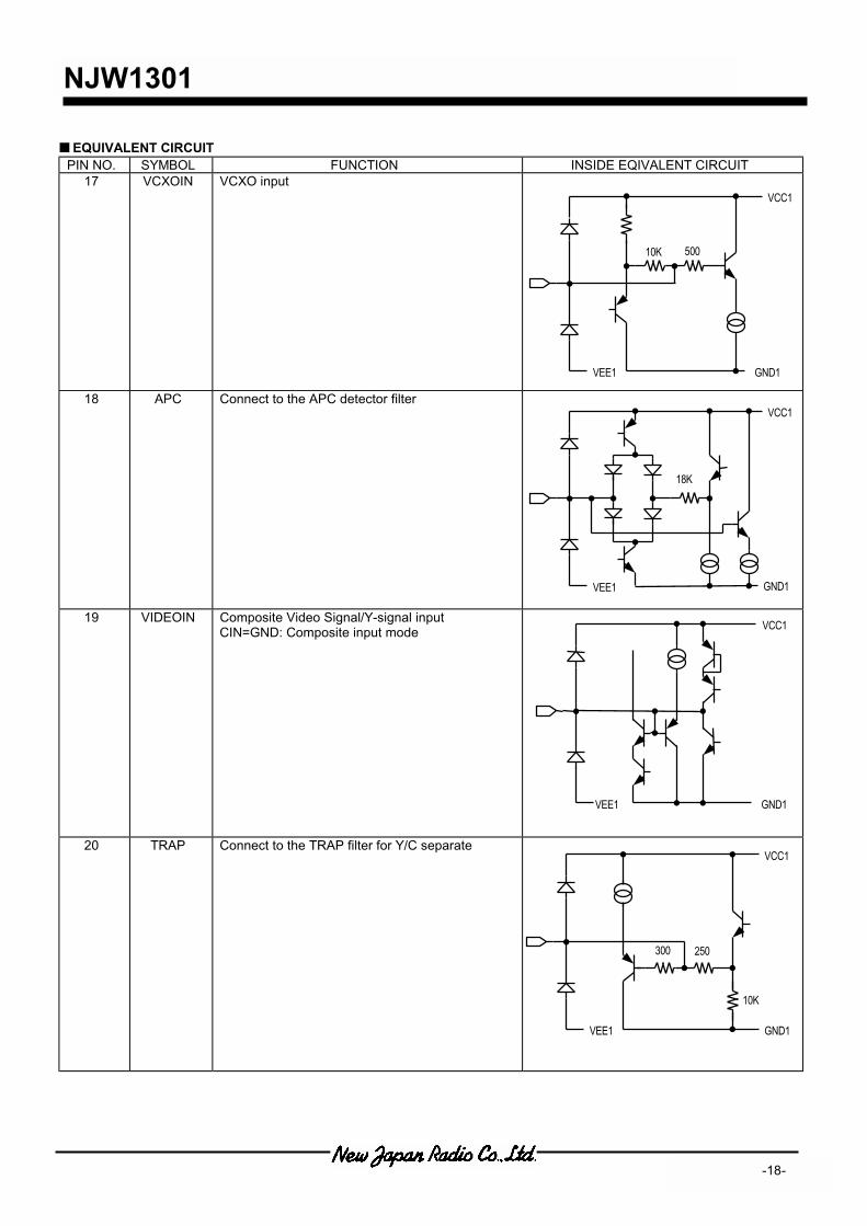
EQUIVALENT CIRCUIT PIN NO. SYMBOL FUNCTION INSIDE EQIVALENT CIRCUIT
17 VCXOIN VCXO input
18 APC Connect to the APC detector filter
19 VIDEOIN Composite Video Signal/Y-signal input CIN=GND: Composite input mode
20 TRAP Connect to the TRAP filter for Y/C separate
500
VCC1
VEE1 GND1
10K
18K
VCC1
VEE1 GND1
VCC1
VEE1 GND1
250
VCC1
VEE1 GND1
300
10K
NJW1301
-19-
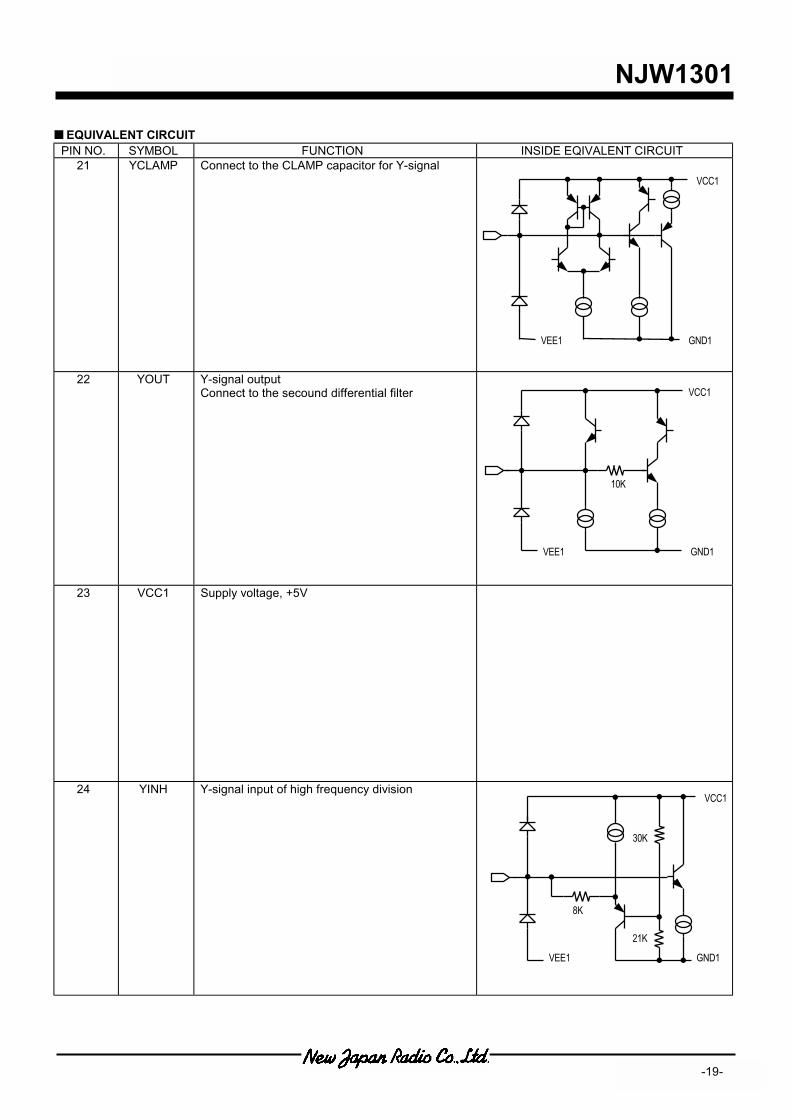
EQUIVALENT CIRCUIT PIN NO. SYMBOL FUNCTION INSIDE EQIVALENT CIRCUIT
21 YCLAMP Connect to the CLAMP capacitor for Y-signal
22 YOUT Y-signal output Connect to the secound differential filter
23 VCC1 Supply voltage, +5V
24 YINH Y-signal input of high frequency division
8K
21K
30K
VCC1
VEE1 GND1
VCC1
VEE1 GND1
VCC1
VEE1 GND1
10K
NJW1301
-20-
EQUIVALENT CIRCUIT PIN NO. SYMBOL FUNCTION INSIDE EQIVALENT CIRCUIT
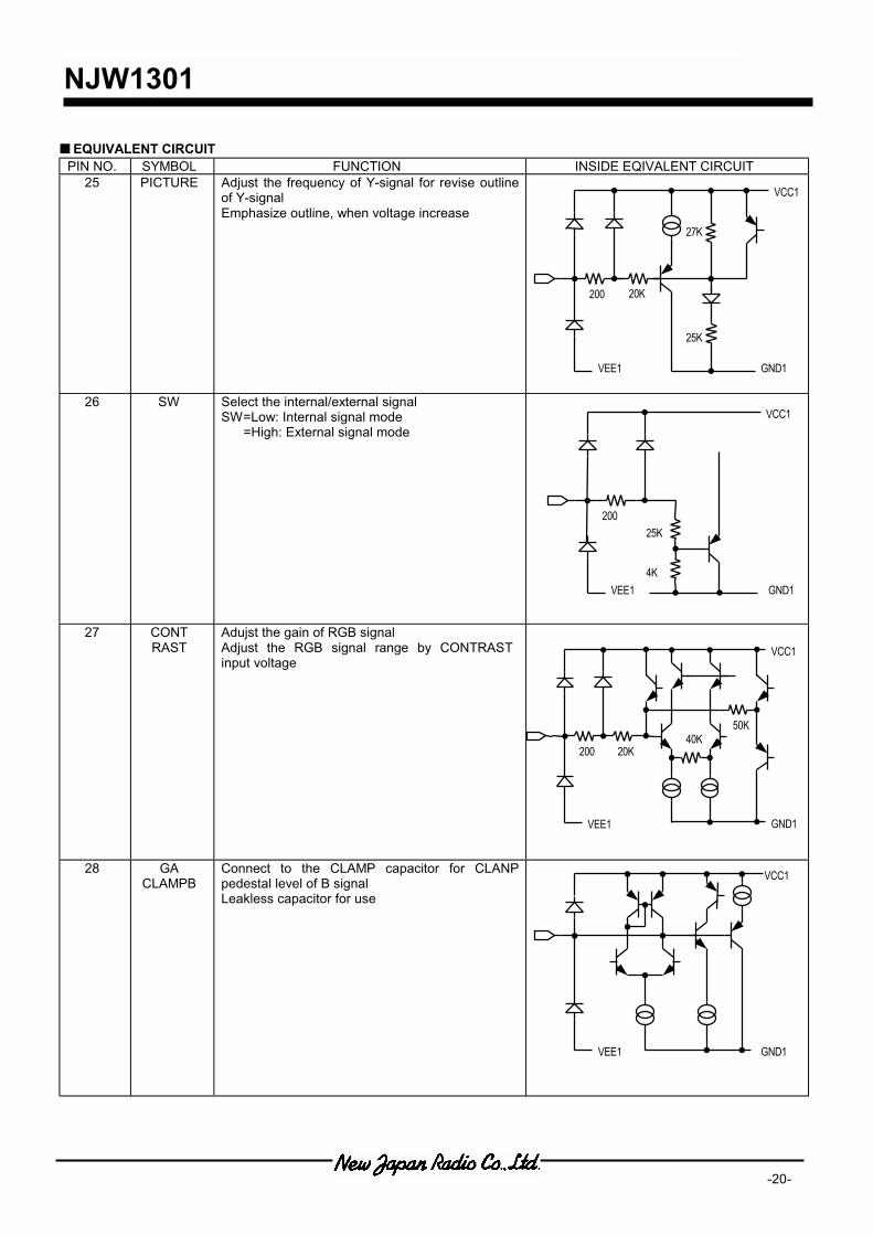
25 PICTURE Adjust the frequency of Y-signal for revise outline of Y-signal Emphasize outline, when voltage increase
26 SW Select the internal/external signal SW=Low: Internal signal mode =High: External signal mode
27 CONT RAST
Adujst the gain of RGB signal Adjust the RGB signal range by CONTRAST input voltage
28 GA CLAMPB
Connect to the CLAMP capacitor for CLANP pedestal level of B signal Leakless capacitor for use
200
4K
25K
VCC1
VEE1 GND1
200 20K
25K
27K
VCC1
VEE1 GND1
50K
20K 200 40K
VCC1
VEE1 GND1
VCC1
VEE1 GND1
NJW1301
-21-
EQUIVALENT CIRCUIT PIN NO. SYMBOL FUNCTION INSIDE EQIVALENT CIRCUIT
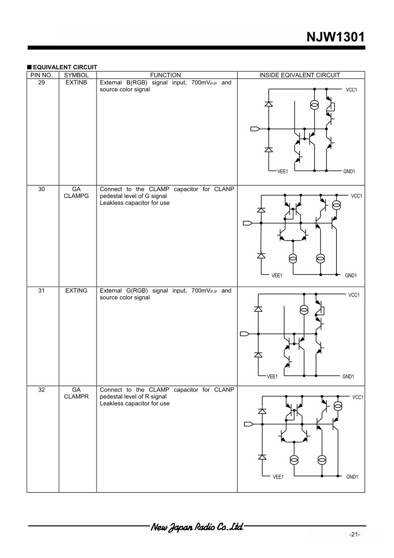
29 EXTINB External B(RGB) signal input, 700mVP-P and source color signal
30 GA CLAMPG
Connect to the CLAMP capacitor for CLANP pedestal level of G signal Leakless capacitor for use
31 EXTING External G(RGB) signal input, 700mVP-P and source color signal
32 GA CLAMPR
Connect to the CLAMP capacitor for CLANP pedestal level of R signal Leakless capacitor for use
VCC1
VEE1 GND1
VCC1
VEE1 GND1
VCC1
VEE1 GND1
VCC1
VEE1 GND1
NJW1301
-22-
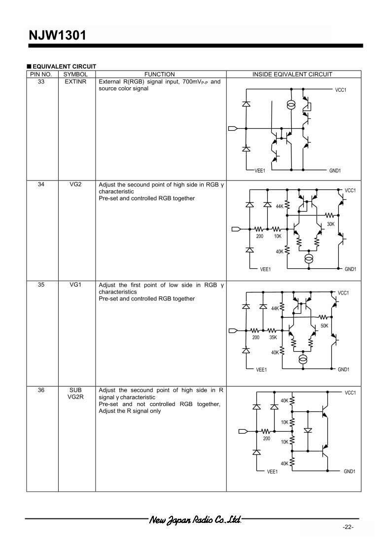
EQUIVALENT CIRCUIT PIN NO. SYMBOL FUNCTION INSIDE EQIVALENT CIRCUIT
33 EXTINR External R(RGB) signal input, 700mVP-P and source color signal
34 VG2 Adjust the secound point of high side in RGB γ characteristic Pre-set and controlled RGB together
35 VG1 Adjust the first point of low side in RGB γ characteristics Pre-set and controlled RGB together
36 SUB VG2R
Adjust the secound point of high side in R signal γ characteristic Pre-set and not controlled RGB together, Adjust the R signal only
VCC1
VEE1 GND1
30K
10K 200
44K
40K
VCC1
VEE1 GND1
50K
35K 200
44K
40K
VCC1
VEE1 GND1
10K
40K
10K 200
40K VCC1
VEE1 GND1
NJW1301
-23-
EQUIVALENT CIRCUIT PIN NO. SYMBOL FUNCTION INSIDE EQIVALENT CIRCUIT
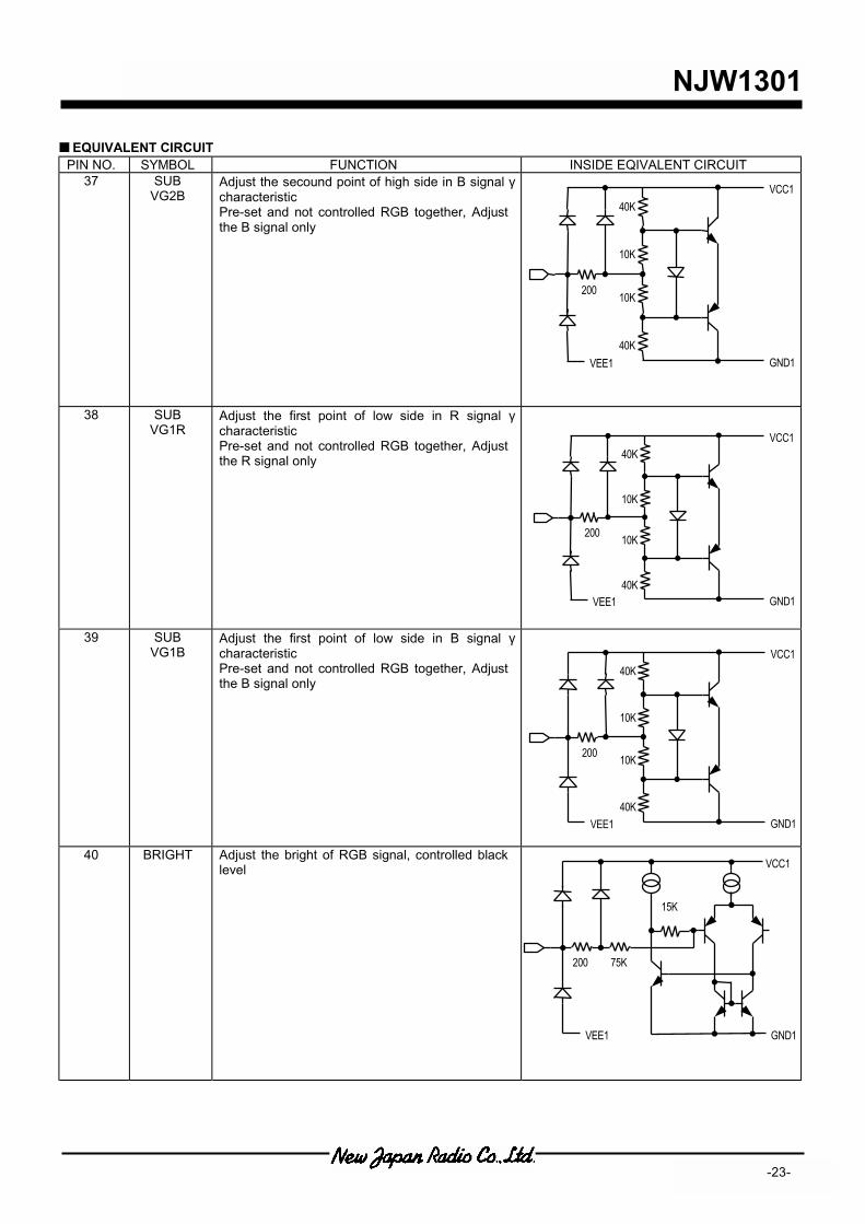
37 SUB VG2B
Adjust the secound point of high side in B signal γ characteristic Pre-set and not controlled RGB together, Adjust the B signal only
38 SUB VG1R
Adjust the first point of low side in R signal γ characteristic Pre-set and not controlled RGB together, Adjust the R signal only
39 SUB VG1B
Adjust the first point of low side in B signal γ characteristic Pre-set and not controlled RGB together, Adjust the B signal only
40 BRIGHT Adjust the bright of RGB signal, controlled black level
10K
40K
10K 200
40K VCC1
VEE1 GND1
15K
200 75K
VCC1
VEE1 GND1
10K
40K
10K 200
40K VCC1
VEE1 GND1
10K
40K
10K 200
40K VCC1
VEE1 GND1
NJW1301
-24-
EQUIVALENT CIRCUIT PIN NO. SYMBOL FUNCTION INSIDE EQIVALENT CIRCUIT
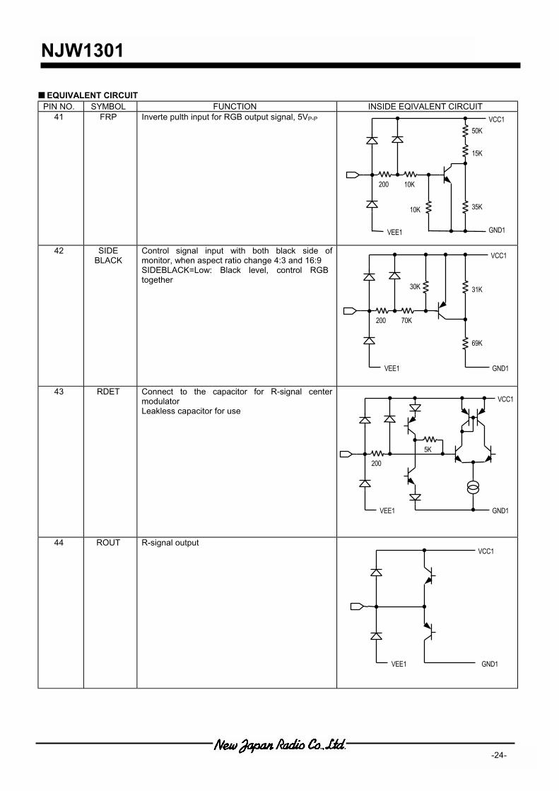
41 FRP Inverte pulth input for RGB output signal, 5VP-P
42 SIDE BLACK
Control signal input with both black side of monitor, when aspect ratio change 4:3 and 16:9 SIDEBLACK=Low: Black level, control RGB together
43 RDET Connect to the capacitor for R-signal center modulator Leakless capacitor for use
44 ROUT R-signal output
200
35K
15K
50K
10K
10K
VCC1
VEE1 GND1
GND1
200
5K
VEE1
VCC1
VCC1
VEE1 GND1
200
69K
31K 30K
70K
VCC1
VEE1 GND1
NJW1301
-25-
EQUIVALENT CIRCUIT PIN NO. SYMBOL FUNCTION INSIDE EQIVALENT CIRCUIT
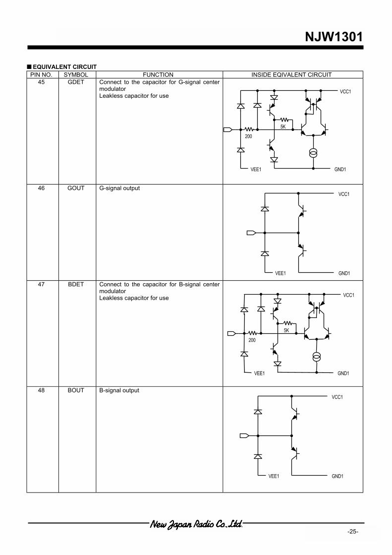
45 GDET Connect to the capacitor for G-signal center modulator Leakless capacitor for use
46 GOUT G-signal output
47 BDET Connect to the capacitor for B-signal center modulator Leakless capacitor for use
48 BOUT B-signal output VCC1
VEE1 GND1
200
5K
VEE1
VCC1
GND1
VCC1
VEE1 GND1
200
5K
VEE1
VCC1
GND1
NJW1301
-26-
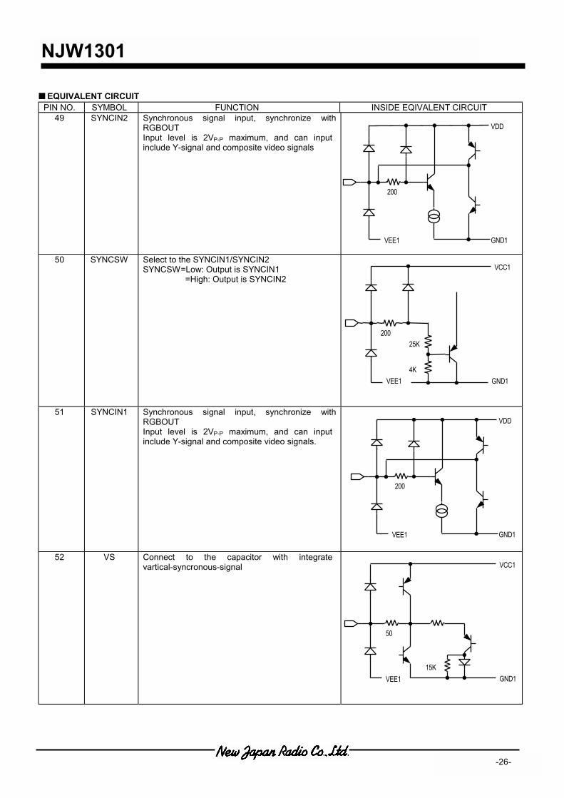
EQUIVALENT CIRCUIT PIN NO. SYMBOL FUNCTION INSIDE EQIVALENT CIRCUIT
49 SYNCIN2 Synchronous signal input, synchronize with RGBOUT Input level is 2VP-P maximum, and can input include Y-signal and composite video signals
50 SYNCSW Select to the SYNCIN1/SYNCIN2 SYNCSW=Low: Output is SYNCIN1 =High: Output is SYNCIN2
51 SYNCIN1 Synchronous signal input, synchronize with RGBOUT Input level is 2VP-P maximum, and can input include Y-signal and composite video signals.
52 VS Connect to the capacitor with integrate vartical-syncronous-signal
200
4K
25K
VCC1
VEE1 GND1
VCC1
VEE1 GND1
50
15K
VDD
VEE1 GND1
200
VDD
VEE1 GND1
200

NJW1301
-27-
EQUIVALENT CIRCUIT PIN NO. SYMBOL FUNCTION INSIDE EQIVALENT CIRCUIT
53 LPF Connect to the AFC filter
54 VCOOUT 32fHVCO output
55 VCOIN 32fHVCO input
56 CSYNC OUT
Composite syncronous signal output, non-inverting and open collector
VDD
GND1
8.2K
8.2K
VEE1
VDD
VEE1 GND1
6K
100
100
4K
4K
VEE1
VDD
GND1
VCC1
GND1
20K 3K
VEE1
3K
NJW1301
-28-
EQUIVALENT CIRCUIT PIN NO. SYMBOL FUNCTION INSIDE EQIVALENT CIRCUIT
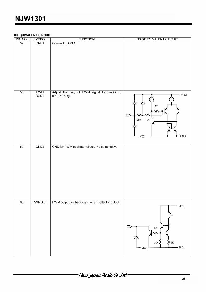
57 GND1 Connect to GND.
58 PWM CONT
Adjust the duty of PWM signal for backlight, 0-100% duty
59 GND2 GND for PWM oscillator circuit, Noise sensitive
60 PWMOUT PWM output for backloght, open collector output
15K
200 75K
VCC1
VEE1 GND2
VCC1
GND2
20K 3K
VEE1
3K
NJW1301
-29-
EQUIVALENT CIRCUIT PIN NO. SYMBOL FUNCTION INSIDE EQIVALENT CIRCUIT
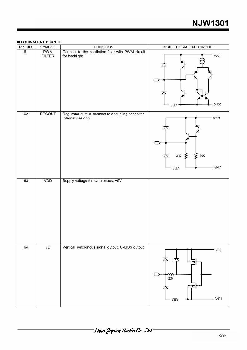
61 PWM FILTER
Connect to the oscillation filter with PWM circuit for backlight
62 REGOUT Regurator output, connect to decupling capacitor Internal use only
63 VDD Supply voltage for syncronous, +5V
64 VD Vertical syncronous signal output, C-MOS output
VDD
GND1 GND1
200
VCC1
24K 30K
VEE1 GND1
VCC1
VEE1 GND2

NJW1301
-30-
PIN FUNCTION at NO USE
No SYMBOL FUNCTION No SYMBOL FUNCTION
1 HD OPEN 33 EXTINR OPEN
2 VCOMAMP OPEN 34 VG2 Input fixed DC voltage
3 VCC3 OPEN: when do not use VCOM 35 VG1 Input fixed DC voltage
4 VCOMIN OPEN 36 SUBVG2R OPEN
5 VCOMCENT OPEN 37 SUBVG2B OPEN
6 VCOMFB OPEN 38 SUBVG1R OPEN
7 VCOMOUT OPEN 39 SUBVG1B OPEN
8 VEE1 GND: when do not use VCOM 40 BRIGHT Input fixed DC voltage
9 ACCDET OPEN 41 FRP Input inverting pulse of RGB output
10 FADJ Connect with 12KΩ 42 SIDEBLACK OPEN
11 KILLER OPEN 43 RDET Connect to capacitor for demodulate R signal
12 PWMREF OPEN 44 ROUT OPEN
13 TINT NTSC MODE: 1V or higher voltage PAL MODE: GND 45 GDET
Connect to capacitor for demodulate G signal
14 CIN GND: when composite signal input OPEN: other 46 GOUT OPEN
15 COLOR OPEN 47 BDET Connect to capacitor for demodulate G signal
16 VCXOOUT OPEN 48 BOUT OPEN
17 VCXOIN OPEN 49 SYNCIN2 Synchronous signal input: 49 or 51pin.
18 APC OPEN 50 SYNCSW OPEN: input SYNC1 only
19 VIDEOIN Connect with 0.01uF to GND 51 SYNCIN1 Synchronous signal input: 49 or 51pin.
20 TRAP OPEN 52 VS Connect to capacitor
21 YCLAMP OPEN 53 LPF Connect to filter
22 YOUT OPEN 54 VCOOUT Connect to Ceramic Oscillation Parts
23 VCC1 Supply voltage (+5V) 55 VCOIN Connect to Ceramic Oscillation Parts
24 YINH Connect with 0.01uF to GND 56 CSYNCOUT OPEN
25 PICTURE OPEN 57 GND1 GND
26 SW OPEN: composite mode only 58 PWMCONT OPEN
27 CONTRAST Input fixed DC voltage 59 GND2 GND
28 GACLAMPB Connect to clamp capacitor 60 PWMOUT OPEN
29 EXTINB OPEN 61 PWMFILTER OPEN
30 GACLAMPG Connect to clamp capacitor 62 REGOUT Connect to capacitor
31 EXTING OPEN 63 VDD OPEN
32 GACLAMPR Connect to clamp capacitor 64 VD OPEN
NJW1301
-31-
None-use PIN Connection 1) Do not use VCOM Driver
The 2pin and 3-7pin are OPEN. The 8pin connect to GND. 2) Do not use composite mode demodulator The 9pin, 11pin, 15-18pin are OPEN. The 13pin is as follows:
13pin Mode 1V or higher NTSC
GND PAL The 19pin, 24pin connect to 0.01uF with GND. The 20-22pin and 25pin are OPEN. 3) Do not use external analog RGB input
The 26pin, 29pin, 31pin and 33pin are OPEN. 4) Do not use the other SYNC IN terminal
The SYNC signal input 49pin or 51pin, either. 5) Do not use HD output and VD output.
The 1pin and ,64pin are OPEN. 6) Do not use C-SYNC output
The 56pin is OPEN. 7) Do not use the adjust terminal of interface and γ circuit
The 36-39pin are OPEN. 8) Do not use SIDE BLACK circuit.
The 42pin is OPEN. 9) Do not use PWM circuit
The 12pin, 58pin, 60pin and 61pin are OPEN.
NJW1301
- 32 -
FUNCTION DESCRIPTION 1. Synchronous Mode
1) Horizontal synchronous There are two synchronous input terminals, first is pin-51 (SYNCIN1) and other is
pin-49 (SYNCIN2). There are no difference, and selected by pin-50 (SYNCSW). The composite-synchronous/synchronous and Y signal input to pin-51/49 either. The
input (pin-51/49) signal is separate by horizontal and vertical synchronous signal. The AFC loop consists of horizontal synchronous signal and 1/32 signal divided 32fH VCO output signal without any adjustment. The pin-56 (CSYNCOUT) is composite-synchronous signal output selected by pin-50, and open collector type.
2) Vertical synchronous
The countdown circuit reset the data to use vertical synchronous signal and 32fH VCO output. This VD pulse is stable even if the weak-signal.
2. Color Signal Play Mode
1) ACC Circuit The chroma signal input to pin-14 (CIN), and detect the burst-signal through the HPF
circuit, and controlled stable burst-signal feedback from demodulate output. When the pin-14 is GND level, the mode is composite input, and pin-19 (VIDEOIN) composite-video signal input to ACC circuit.
2) APC Circuit, and VCXO
The burst signal level of chroma is constant by ACC circuit. The PLL circuit consists of VCXO and locked burst signal. The pin-13 (TINT) input DC voltage adjust the VCXO phase, and adjust the demodulate axis. When the pin-13 is GND, the mode is PAL, and only accepts analog RGB input.
3) Color Killer
The chroma signal is output to demodulator when PLL locked, and the color killer is –42dB.
4) Color Circuit
This circuit adjusts the color TINT. The pin-15 (COLOR) adjusts the chroma signal range from ACC circuit. This signal demodulator without burst signal by burst gate pulse (BGP).
5) DEMOD
This DEMOD circuits demodulate color differential signal after the ACC circuit. The RGB signal consists of color differential and Y signal by matrix circuit, and input to Int./Ext. signal switches.
NJW1301
- 33 -
3. Y-signal Mode
1) TRAP The composite video signal input to pin-19 (VIDEOIN) without the chroma by TRAP
circuit. The TPAP frequency is 3.58MHz, and not through when Y/C input mode.
2) Picture Circuit The Y/composite-signal input to pin-19 (VIDEOIN) without the synchronous signal. The
pin-25 (PICTURE) adjusts the frequency characteristic around 2MHz and emphasizes the outline. The pin-25 level emphasizes outline depend on the DC voltage. The Y-signal output pin-22 (YOUT), and input to pin-24 (YINH) through the external second differential circuit.
4. INT./EXT. Signal Switch Mode
The analog RGB signal (0.7VP-P typ.) input to pin-29, pin-31, and pin-33, and these signal clamps pedestal. The ext-signal select Y/C-signal or Int-signal by pin-26 (SW).
5. RGB SIGNAL MODE
1) Contrast The pin-27 (CONTRAST) adjusts the all of RGB signal, which is black-to-white range.
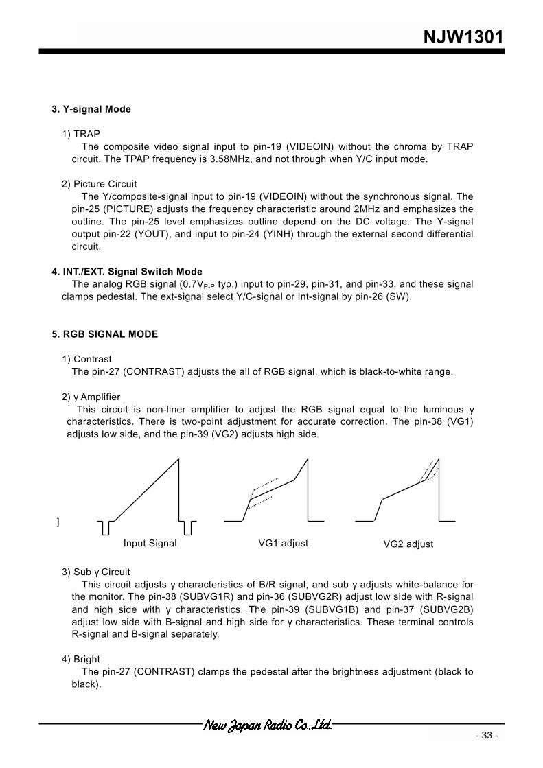
2) γ Amplifier
This circuit is non-liner amplifier to adjust the RGB signal equal to the luminous γ characteristics. There is two-point adjustment for accurate correction. The pin-38 (VG1) adjusts low side, and the pin-39 (VG2) adjusts high side.
]
3) Sub γ Circuit This circuit adjusts γ characteristics of B/R signal, and sub γ adjusts white-balance for
the monitor. The pin-38 (SUBVG1R) and pin-36 (SUBVG2R) adjust low side with R-signal and high side with γ characteristics. The pin-39 (SUBVG1B) and pin-37 (SUBVG2B) adjust low side with B-signal and high side for γ characteristics. These terminal controls R-signal and B-signal separately.
4) Bright
The pin-27 (CONTRAST) clamps the pedestal after the brightness adjustment (black to black).
VG1 adjust Input Signal VG2 adjust
NJW1301
- 34 -
5) Side Black The side-black circuit output black level, when the mode is black mask for wide picture. The RGB signal is black level when pin-42 (SIDEBLACK) input signal is low period only.
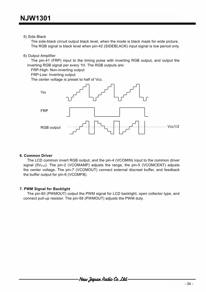
6) Output Amplifier
The pin-41 (FRP) input to the timing pulse with inverting RGB output, and output the inverting RGB signal per every 1H. The RGB outputs are:
FRP-High: Non-inverting output FRP-Low: Inverting output The center voltage is preset to half of Vcc.
6. Common Driver
The LCD common invert RGB output, and the pin-4 (VCOMIN) input to the common driver signal (5VP-P). The pin-2 (VCOMAMP) adjusts the range, the pin-5 (VCOMCENT) adjusts the center voltage. The pin-7 (VCOMOUT) connect external discreet buffer, and feedback the buffer output for pin-6 (VCOMFB).
7. PWM Signal for Backlight
The pin-60 (PWMOUT) output the PWM signal for LCD backlight, open collector type, and connect pull-up resistor. The pin-58 (PWMOUT) adjusts the PWM duty.
Yin
FRP
RGB output Vcc1/2
NJW1301
MEMO
[CAUTION] The specifications on this databook are only
given for information , without any guarantee as regards either mistakes or omissions. The application circuits in this databook are described only to show representative usages of the product and not intended for the guarantee or permission of any right including the industrial rights.


![Liste des icônes – Z41 - Zennio · 2020. 5. 11. · Liste d'icônes ZN1VI -TP41 N Version du programme d'application [2.0] Édition: [2.0]_a](https://img.pdfslide.us/doc/110x75/60affe09d1019e47b1476129/liste-des-icnes-a-z41-zennio-2020-5-11-liste-dicnes-zn1vi-tp41-n.jpg)