Embed Size (px)
Citation preview
International Journal of VLSI design & Communication Systems (VLSICS) Vol.2, No.2, June 2011
DOI : 10.5121/vlsic.2011.2207 78
NEW DESIGN METHODOLOGIES FOR
HIGH-SPEED MIXED-MODE CMOS
FULL ADDER CIRCUITS
Subodh Wairya1, Rajendra Kumar Nagaria
2, Sudarshan Tiwari
3
Department of Electronics & Communication Engineering,
M.N.N.I.T, Allahabad, India [email protected],[email protected],[email protected]
ABSTRACT
This paper presents the design of high-speed full adder circuits using a new CMOS mixed mode logic
family. The objective of this work is to present a new full adder design circuits combined with current mode
circuit in one unit to implement a full adder cell. This paper also discusses a high- speed hybrid majority
function based 1-bit full adder that uses MOS capacitors (MOSCAP) in its structure with conventional
static and dynamic CMOS logic circuit. The static Majority function (bridge) design style enjoys a high
degree of regularity and symmetric higher density than the conventional CMOS design style as well as
lower power consumption by using bridge transistors. This technique helps in reducing power
consumption, propagation delay, and area of digital circuits while maintaining low complexity of mixed-
mode logic designs. Dynamic CMOS circuits enjoy area, delay and testability advantages over static
CMOS circuits. Simulation results illustrate the superiority of the new designed adder circuits against the
reported conventional CMOS, dynamic and majority function adder circuits, in terms of power, delay,
power delay product (PDP) and energy delay product (EDP). The design is implemented on UMC 0.18µm
process models in Cadence Virtuoso Schematic Composer at 1.8 V single ended supply voltage and
simulations are carried out on Spectre S.
.
KEYWORDS
Full adder, Majority-Not gate, Dynamic circuits, MOSCAP, Power-delay product (PDP), Very Large Scale
Integrated (VLSI) Circuits, Current mode logic, Hybrid XOR-XNOR circuit, Bridge full adder.
1. INTRODUCTION
Low-power design of VLSI circuits has been identified as a critical technological need in recent
years due to high demand for portable consumer electronics products. With the explosive growth
in laptops, portable personal communication systems and the evolution of the shrinking
technology, the research effort in low-power microelectronics has been intensified and low-power
VLSI systems have emerged high in demand. Adder is one of the most important components of a
CPU (central processing unit), Arithmetic logic unit (ALU), floating-point unit and address
generation unit like cache or memory access unit.
Digital circuit designers have always been encountered in a tradeoff between speed and power
consumption to improve their design’s performance. There are standard implementations with
various logic styles that have been used in the past to design full-adder cells [16-38] and these are
used for the comparison in this paper. Although they all have similar function, the way of
producing the intermediate nodes and the transistor count are varied. Different logic styles tend to
favour one performance aspect at the expense of the others. The logic style used in logic gates
basically influences the speed, size, power dissipation, and the wiring complexity of a circuit. The
circuit delay is determined by the number of inversion levels, the number of transistors in series,
the transistor sizes (i.e. channel widths) and the intra-cell wiring capacitances. The circuit

International Journal of VLSI design & Communication Systems (VLSICS) Vol.2, No.2, June 2011
79
size depends on the number of transistors, their size and the wiring complexity. Some of them use
one logic style for the whole full adder and others use more than one logic style for their
implementation.
In addition, full-adders are important components in other applications such as digital signal
processing (DSP) architectures and microprocessor. Arithmetic functions such as addition,
subtraction, multiplication and division are some examples which use adder as a main building
block [1-7]. In nano-scaling, the biggest power consumption is static power dissipation.
Depending on the application, the kind of circuit implemented, and the design techniques used,
different performance aspects become important, disallowing the formulation of universal rules
for optimal logic styles.
There are two types of full adders in case of logic structure. One is static style and the other is
dynamic style. Static full adders are commonly more reliable, simpler and of lower power than
dynamic ones. Dynamic is an alternative logic style to design a logic function. It has some
advantages in comparison with static mode such as faster switching speeds, no static power
consumption, non-ratioed logic, full swing voltage levels and less number of transistors. For an N
input logic function, it requires N+2 transistors versus 2N transistors in the standard CMOS logic.
The area advantage comes from the fact that the pMOS network of a dynamic CMOS gate
consists of only one transistor. This also results in a reduction in the capacitive load at the output
node, which is the basis for the high-speed advantage. Dynamic CMOS logic style provides high
performance because this logic style is constructed with only high mobility nMOS transistors.
Also, due to the absence of the pMOS transistors, the input capacitance is lower. Dynamic full
adders suffer from charge sharing, high power due to high switching activity, clock load and
complexity. However, dynamic full adders are faster and some times more compact than static
full adders. Many researchers have combined these two structures and have proposed hybrid
dynamic-static full adders.
Domino CMOS circuits fall under the category of Dynamic CMOS logic, which gives advantage
in terms of testability over static CMOS circuits [31]. The inherent problem with Domino CMOS
circuit is that it suffers from noise margin problem due to charge redistribution between parasitic
capacitances at the internal nodes of the circuit, which may result in false output. Domino is
nonratioed logic with faster switching speed and less silicon area required as compared to the full
static CMOS logic [3-5]. Domino logic consists of a single clock, which is used to precharge the
dynamic node of the circuit in precharge phase and to evaluate the function made by nMOS
network in evaluation phase. As technology scaling continues, allowing for more logic gates per
chip, complex parallel prefix schemes, and fast adder design become viable. In modern CMOS
technologies, transistor sizing has been used to find the optimal trade off between speed and
energy consumption of an adder [32].
To summarize, some of the performance criteria are considered in the design and evaluation of
adder cells and some are utilized for the ease of design, robustness, silicon area, delay, and power
consumption. The rest of this paper is organized as follows: Power consideration in digital CMOS
circuits is explained in Section 2. Section 3 explores a review of the full adder design in different
logic styles. A review of logic styles with majority functions have been discussed in Section 4. In
Section 5, implementations of Majority Function based hybrid full adder methodologies (HyFA1-
HyFA5) and mixed mode full adder designs (MixFA1-MixFA3) are discussed. In Section 6 the
reported and new majority function based full adder design topologies are simulated and the
simulation results analyzed and compared. Finally, Section 7 concludes the paper.

International Journal of VLSI design & Communication Systems (VLSICS) Vol.2, No.2, June 2011
80
2. POWER CONSIDERATION IN DIGITAL CMOS
Power is one of the vital resources. Hence, the designers try to save it when designing a system.
Power dissipation is dependent on the switching activity, node capacitances (made up of gate,
diffusion, and wire capacitances), and control circuit size. There are four source of power
dissipation: dynamic switching power due to the charging and discharging of circuit capacitance,
leakage current power from reverse biased diodes and sub-threshold conduction, short-circuit
current power due to finite signal rise/fall times, and static biasing power found in some logic
styles (i.e. pseudo-nMOS).
Dynamic switching power is the major component of overall power dissipation, the low-power
design methodology concentrates on minimizing total capacitance, supply voltage, and frequency
of transistor. For most CMOS circuit design, the short circuit power dissipation is approximately
5-10% of the total dynamic power. The sub-threshold current is proportional to the transistor
device size (W/L) and an exponential function of the supply voltage. Thus, the current may be
minimized by reducing the transistor sizes, and by reducing the supply voltage.
Scaling in the supply voltage appears to be the most well-known means to reduce power
consumption. However, the lower-supply voltage increases circuit delay and degrades the
drivability of cells designed with certain logic style. One of the important obstacles in decreasing
the supply voltage is the large transistor count and Vth loss problem. By selecting proper (W/L)
ratio we can minimize the power dissipation without decreasing the supply voltage.
3. REVIEW OF FULL ADDER TOPOLOGIES
In recent years several variants of different logic styles have been proposed to implement 1-bit
adder cells [33-50]. These have investigated different approaches realizing adders using CMOS
technology, each having its own pros and cons. There are various issues related to the full adders.
Some of them are, power consumption, performance, area, noise immunity, regularity and good
driving ability. Voltage mode in a general shape contains two networks. Each of these networks
contains transistors which behave like a switch. The pull up network is responsible to produce
logical “1” and the pull down network is responsible to produce logical “0”. In these circuits, a
group of switches is connected and the other group is disconnected in every instant. So we need
two groups of switches in constructing these gates, which usually have a contrary operation with
each other and is dependent to the output function. The CMOS family gates are good example for
comprehension of the structure of these circuits. The logical Boolean expressions between the
inputs and outputs are expressed as:
C.B.AC.B.AC.B.AC.B.ASum +++= 1
C.B.AC.B.AC.B.AC.B.AMajorityCarry +++== C.AC.BB.A)BA(CB.A ++=++= 2
Concerns about energy consumption have force digital designers to develop techniques for
improving energy efficiency. Many approaches have been proposed for the optimal construction
of high-performance VLSI adders in a given technology such as: Proper selection of logic family
and prefix, reducing the number of logic stages without increasing gate count, reducing the
number of logic gates, reducing switching activity and reducing the wiring complexity [8-15].
The logic circuits are characterized based on the following logic conditions as defined below:
Logic Depth (LD): The maximum number of logic stages from output to inputs. Each logic gate
is counted as a stage for fully static implementation. However, in compound designs, the
International Journal of VLSI design & Communication Systems (VLSICS) Vol.2, No.2, June 2011
81
dynamic gate and the following static gate are counted as one stage. The number of stages
depends on the prefix of design. Minimum depth adders are used when high performance is
required.
Logic Family Selection: In VLSI design, the selection of logic family is dictated by the system
performance target. In structures where the performance target is relaxed or where energy is the
primary constraint, static circuits are preferred due to their lower switching activity. In addition to
that, static circuits are robust and have become more preferable as technology scales down.
However, in high-performance microprocessors, dynamic circuits are often required in order to
achieve desired target frequency. There are two types of dynamic circuit families used in modern
digital systems: (a) dynamic CMOS domino and (b) CMOS compound domino. The main
difference between these families is that CMOS domino utilizes a static inverter at the output,
while CMOS compound domino uses a static inverting logic stage. This helps in reducing the
power by eliminating power hungry dynamic stages and bundling their functionality in the static
CMOS inverting stage. As a summary, static circuits are good for power and domino circuits are
good for speed. Compound domino designs can combine the speed advantage of dynamic designs
and the power advantage of static designs.
Prefix (p): The number of bits combined at each logic stage as defined above. For example, the
two-input dynamic gate and the following two-input static gate is defined as prefix-2 stages for
domino designs. The two-input dynamic gate and the following two-input static gate is defined as
a prefix-4 stage for compound domino designs. Prefix adders are consisting of two blocks,
namely, Sum and Carry blocks. A basic cell in digital computing systems is 1-bit full adder which
has 1-bit inputs (A, B, C) and two 1-bit outputs (Sum and Carry).
Prefix Selection: In static CMOS logic, the prefix is mostly limited to 2 because of transistor
stack height limitation while dynamic designs enable to use of higher prefixes. As prefix of the
design increases the logic depth decreases and it is expected to lead to delay improvement.
However, higher prefix requires more complex gates with increased stack height resulting in
higher gate delay. Therefore, there is an optimal prefix that depends on the design constraints and
implementation.
Load Buffering: Addition of inverters is used to drive the output load because inverters are the
most energy-efficient drivers. Extra delays come from the parasitic and effort delay of the added
inverters. However, the delay of the original circuit will be reduced since it drives added inverters
that are smaller than the output load. In addition, extra energy is consumed by added inverters but
the original circuit’s size is reduced. There is a tradeoff between the saved delay/energy and extra
delay/energy coming from the added inverters. Load buffering provides energy savings for
heavily loaded designs under the same delay constraints. As the load is reduced, the energy
saving of the adder circuit cannot compensate for the extra energy consumed by the extra
inverters. The energy saving of load buffering depends on the driving strength of the original
circuit and the path gain.
3.1 Static Full Adder Topologies
Static CMOS logic styles have been used to implement the low-power 1-bit adder cells. In
general, they can be broadly divided into two major categories: the Complementary CMOS and
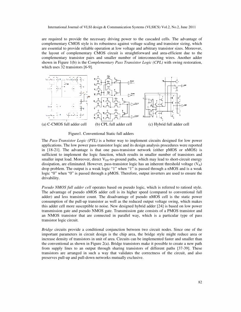
the Pass-Transistor logic circuits. The complementary CMOS (C-CMOS) full adder of Figure
1(a) is based on the regular CMOS structure with P type Metal Oxide Semiconductor (pMOS)
pull-up and N type Metal Oxide Semiconductor (nMOS) pull-down transistors [3-8]. The series
transistors in the output stage form a weak driver. Therefore, additional buffers at the last stage
International Journal of VLSI design & Communication Systems (VLSICS) Vol.2, No.2, June 2011
82
are required to provide the necessary driving power to the cascaded cells. The advantage of
complementary CMOS style is its robustness against voltage scaling and transistor sizing, which
are essential to provide reliable operation at low voltage and arbitrary transistor sizes. Moreover,
the layout of complementary CMOS circuit is straightforward and area-efficient due to the
complementary transistor pairs and smaller number of interconnecting wires. Another adder
shown in Figure 1(b) is the Complementary Pass Transistor Logic (CPL) with swing restoration,
which uses 32 transistors [6-9].
(a) C-CMOS full adder cell (b) CPL full adder cell (c) Hybrid full adder cell
Figure1. Conventional Static full adders
The Pass-Transistor Logic (PTL) is a better way to implement circuits designed for low power
applications. The low power pass-transistor logic and its design analysis procedures were reported
in [18-21]. The advantage is that one pass-transistor network (either pMOS or nMOS) is
sufficient to implement the logic function, which results in smaller number of transistors and
smaller input load. Moreover, direct VDD-to-ground paths, which may lead to short-circuit energy
dissipation, are eliminated. However, pass-transistor logic has an inherent threshold voltage (Vth)
drop problem. The output is a weak logic “1” when “1” is passed through a nMOS and is a weak
logic “0” when “0” is passed through a pMOS. Therefore, output inverters are used to ensure the
drivability.
Pseudo NMOS full adder cell operates based on pseudo logic, which is referred to ratioed style.
The advantage of pseudo nMOS adder cell is its higher speed (compared to conventional full
adder) and less transistor count. The disadvantage of pseudo nMOS cell is the static power
consumption of the pull-up transistor as well as the reduced output voltage swing, which makes
this adder cell more susceptible to noise. New designed hybrid adder [24] is based on low power
transmission gate and pseudo NMOS gate. Transmission gate consists of a PMOS transistor and
an NMOS transistor that are connected in parallel way, which is a particular type of pass
transistor logic circuit.
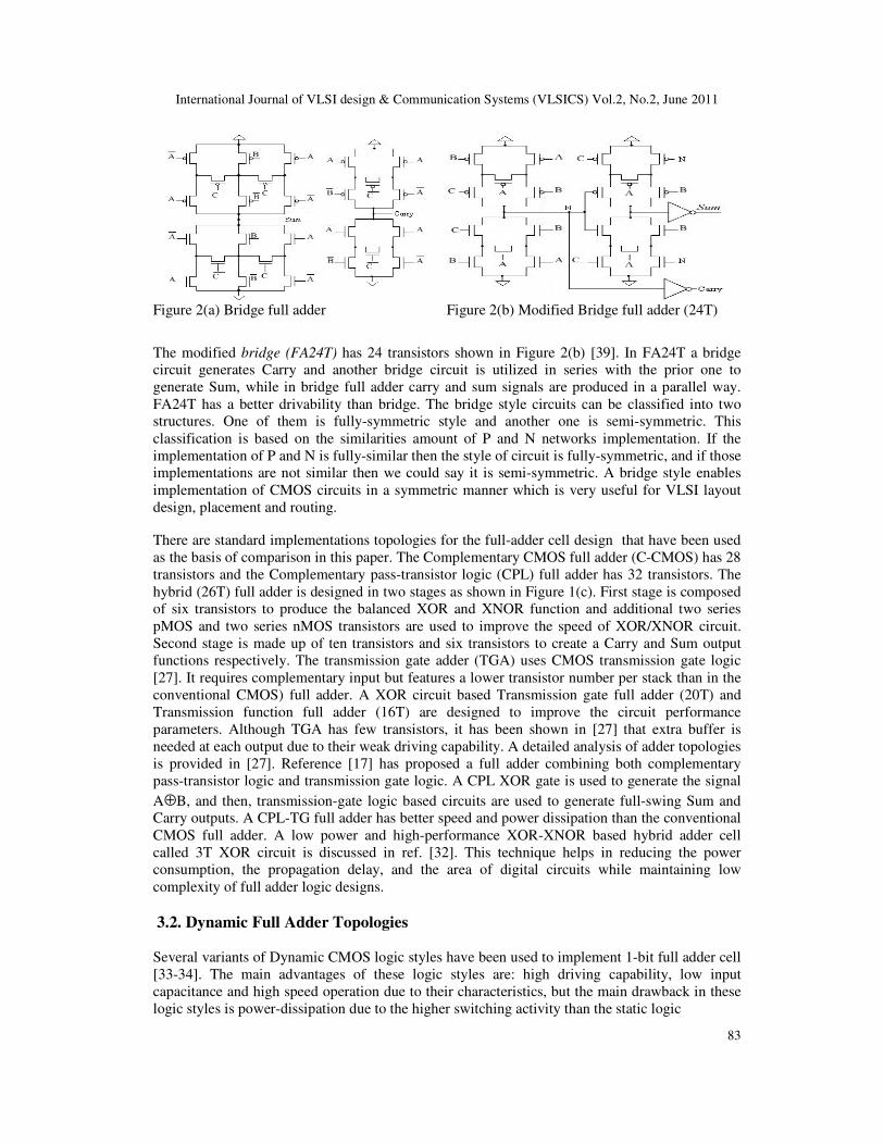
Bridge circuits provide a conditional conjunction between two circuit nodes. Since one of the
important parameters in circuit design is the chip area, the bridge style might reduce area or
increase density of transistors in unit of area. Circuits can be implemented faster and smaller than
the conventional as shown in Figure 2(a). Bridge transistors make it possible to create a new path
from supply lines to an output through sharing transistors of different paths [37-39]. These
transistors are arranged in such a way that validates the correctness of the circuit, and also
preserves pull-up and pull-down networks mutually exclusive.
International Journal of VLSI design & Communication Systems (VLSICS) Vol.2, No.2, June 2011
83
Figure 2(a) Bridge full adder Figure 2(b) Modified Bridge full adder (24T)
The modified bridge (FA24T) has 24 transistors shown in Figure 2(b) [39]. In FA24T a bridge
circuit generates Carry and another bridge circuit is utilized in series with the prior one to
generate Sum, while in bridge full adder carry and sum signals are produced in a parallel way.
FA24T has a better drivability than bridge. The bridge style circuits can be classified into two
structures. One of them is fully-symmetric style and another one is semi-symmetric. This
classification is based on the similarities amount of P and N networks implementation. If the
implementation of P and N is fully-similar then the style of circuit is fully-symmetric, and if those
implementations are not similar then we could say it is semi-symmetric. A bridge style enables
implementation of CMOS circuits in a symmetric manner which is very useful for VLSI layout
design, placement and routing.
There are standard implementations topologies for the full-adder cell design that have been used
as the basis of comparison in this paper. The Complementary CMOS full adder (C-CMOS) has 28
transistors and the Complementary pass-transistor logic (CPL) full adder has 32 transistors. The
hybrid (26T) full adder is designed in two stages as shown in Figure 1(c). First stage is composed
of six transistors to produce the balanced XOR and XNOR function and additional two series
pMOS and two series nMOS transistors are used to improve the speed of XOR/XNOR circuit.
Second stage is made up of ten transistors and six transistors to create a Carry and Sum output
functions respectively. The transmission gate adder (TGA) uses CMOS transmission gate logic
[27]. It requires complementary input but features a lower transistor number per stack than in the
conventional CMOS) full adder. A XOR circuit based Transmission gate full adder (20T) and
Transmission function full adder (16T) are designed to improve the circuit performance
parameters. Although TGA has few transistors, it has been shown in [27] that extra buffer is
needed at each output due to their weak driving capability. A detailed analysis of adder topologies
is provided in [27]. Reference [17] has proposed a full adder combining both complementary
pass-transistor logic and transmission gate logic. A CPL XOR gate is used to generate the signal
A⊕B, and then, transmission-gate logic based circuits are used to generate full-swing Sum and
Carry outputs. A CPL-TG full adder has better speed and power dissipation than the conventional
CMOS full adder. A low power and high-performance XOR-XNOR based hybrid adder cell
called 3T XOR circuit is discussed in ref. [32]. This technique helps in reducing the power
consumption, the propagation delay, and the area of digital circuits while maintaining low
complexity of full adder logic designs.
3.2. Dynamic Full Adder Topologies
Several variants of Dynamic CMOS logic styles have been used to implement 1-bit full adder cell
[33-34]. The main advantages of these logic styles are: high driving capability, low input
capacitance and high speed operation due to their characteristics, but the main drawback in these
logic styles is power-dissipation due to the higher switching activity than the static logic

International Journal of VLSI design & Communication Systems (VLSICS) Vol.2, No.2, June 2011
84
designs. There are two phases in dynamic logic. For a structure where output node is connected to
VDD by a precharge pMOS transistor, there has to be a pull-down network implemented in nMOS.
When Clock=0, circuit enters the precharge phase and when Clock=1, the evaluation phase starts.
All the input values should be changed at precharge phase to avoid the charge sharing problem
and incorrect functionality. It is because once the output discharges at evaluation phase, there will
be no path between output and VDD to charge it again until the next precharge phase.The Sum
output function can be described by the following equation:
Sum = Carry . (A + B + C) + A.B.C 3
3(a) NP CMOS logic 3(b) Dynamic NP-CMOS (Dyn1) 3(c) PN logic
The NP complementary dynamic CMOS full adder [7] is shown in Figure 3(a). It is based on
regular dynamic CMOS designing in two levels with Zipper (NP) technique. The advantage of
NP complementary dynamic CMOS style is its performance, but power consumption is high. The
reported circuit is to use NP-CMOS (Zipper) logic style to implement the 1-bit full adder cell as
shown in Figure 4(a) [34]. In the first stage the Carry function is obtained by using the bridge
style [9]. In the second stage the Sum function is gained according to the equation (3). This
design has 16 transistors. It has full swing voltage levels. Clock and Clock signals cause both
stages of the circuit to enter the evaluation phase simultaneously. The PN complementary
dynamic CMOS full adder is shown in Figure 3(c). It is implemented in two level dynamic
CMOS logic style with PN technique.
4(a) Multi-output Dynamic logic 4(b) Multi-output Dynamic (Dyn2) adder
Figure 3-4 Conventional Dynamic full adders
International Journal of VLSI design & Communication Systems (VLSICS) Vol.2, No.2, June 2011
85
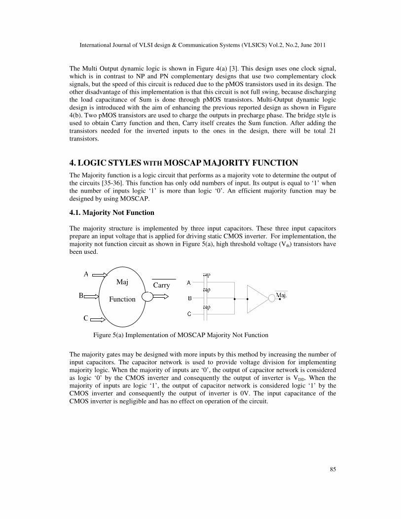
The Multi Output dynamic logic is shown in Figure 4(a) [3]. This design uses one clock signal,
which is in contrast to NP and PN complementary designs that use two complementary clock
signals, but the speed of this circuit is reduced due to the pMOS transistors used in its design. The
other disadvantage of this implementation is that this circuit is not full swing, because discharging
the load capacitance of Sum is done through pMOS transistors. Multi-Output dynamic logic
design is introduced with the aim of enhancing the previous reported design as shown in Figure
4(b). Two pMOS transistors are used to charge the outputs in precharge phase. The bridge style is
used to obtain Carry function and then, Carry itself creates the Sum function. After adding the
transistors needed for the inverted inputs to the ones in the design, there will be total 21
transistors.
4. LOGIC STYLES WITH MOSCAP MAJORITY FUNCTION
The Majority function is a logic circuit that performs as a majority vote to determine the output of
the circuits [35-36]. This function has only odd numbers of input. Its output is equal to ‘1’ when
the number of inputs logic ‘1’ is more than logic ‘0’. An efficient majority function may be
designed by using MOSCAP.
4.1. Majority Not Function
The majority structure is implemented by three input capacitors. These three input capacitors
prepare an input voltage that is applied for driving static CMOS inverter. For implementation, the
majority not function circuit as shown in Figure 5(a), high threshold voltage (Vth) transistors have
been used.
Figure 5(a) Implementation of MOSCAP Majority Not Function
The majority gates may be designed with more inputs by this method by increasing the number of
input capacitors. The capacitor network is used to provide voltage division for implementing
majority logic. When the majority of inputs are ‘0’, the output of capacitor network is considered
as logic ‘0’ by the CMOS inverter and consequently the output of inverter is VDD. When the
majority of inputs are logic ‘1’, the output of capacitor network is considered logic ‘1’ by the
CMOS inverter and consequently the output of inverter is 0V. The input capacitance of the
CMOS inverter is negligible and has no effect on operation of the circuit.
Maj
Function
A
B
C
Carry

International Journal of VLSI design & Communication Systems (VLSICS) Vol.2, No.2, June 2011
86
4.2. Majority Not Function based Static Logic Gates
Figure 5(b) MOSCAP 10.4f F (NAND, NOR and Majority-NOT) gate
Majority Not function is a logic gate with odd numbers of inputs, and its output is high when the
numbers of logic ‘1’s is less then the number of ‘logic 0’s in the input of the logic gate. The
Majority not function is implemented efficiently by using only capacitors and a static CMOS
inverter. Figure 5(b) shows a circuit used to implement majority-not function with inverter
utilizing high-Vth for both nMOS and pMOS. This circuit can be used to implement NAND gate
using high-Vth nMOS and low-Vth pMOS, and NOR gate using low-Vth nMOS and high-Vth
pMOS.
4.3. Majority Function based Dynamic Logic Gates
The design of three input Majority Not Function, NAND and NOR dynamic CMOS circuits are
shown in Figure 6 [52]. It uses three input capacitances in order to implement different functions
with unique circuit implementation. As shown, the number of transistors is reduced leading to
lower power dissipation. The three inputs Majority Not Function which is implemented with pre-
charge and pre-discharge dynamic CMOS circuit are shown in Figure 6(a) &6(b). In order to
make the pre-discharge circuit working as a Majority Not Function, the threshold voltages of
pMOS transistor is reduced to-0.9 V and the values of input capacitances is selected accurately as
shown in Figure 6 [52]. This reduction in Vth influenced the performance of the circuit, but on the
other side the lower power dissipation is gained.
In order to make the circuit shown in Figure 6(c) working as a Majority Not Function, transistor
MN1must be turned on (Vgs>Vth) when at least two out of the three inputs are high, but if the
transistor turns on when one of its input goes high, the NOR function is implemented and for
implementing NAND function, transistors MN1 must be turned on whenever all the inputs are
high. All these function could be designed by selecting the correct values for input capacitances.
The values of input capacitances for building majority not Function, NAND and NOR is shown in
Figure 6. Simulation results in Table 1 illustrate the comparison of logic gates with MOSCAP
based majority function, static and dynamic logic style at 1V [49].
(a) Majority Function (pre-charge) (b) Majority Function (pre-discharge)

International Journal of VLSI design & Communication Systems (VLSICS) Vol.2, No.2, June 2011
87
(c) Majority Not Function (d) NAND (e) NOR
Figure 6. Dynamic CMOS MOSCAP (NAND, NOR and Majority-NOT) logic gate
Table 1. Simulation results of NAND, NOR, Majority Not gates in 0.18µm at room temp.
Design Static logic Majority Function (Dynamic logic)
Delay
(ps)
Power
(µw)
PDP
(10-18
j)
Delay
(ps)
Power(
µw)
PDP
(10-18
j)
Delay
(ps)
Power
(µw)
PDP
(10-
18j)
NAND 36 0.041 1.47 23 0.038 0.87 27 0.051 1.38
NOR 40 0.042 1.68 27 0.039 1.05 26 0.051 1.33
Maj.NOT 43 0.048 2.06 18 0.038 0.68 36 0.049 1.76
4.4. Majority Function based Current Mode Logic
Current Mode Logic (CML) has some advantages over voltage mode MVL. Implementing
voltage-mode multiple-valued logic (MVL) requires partitioning the total voltage range, zero to
supply voltage in to many discrete levels. Thus, the dynamic range and the noise margin are
highly dependent on the supply voltage. In current-mode circuits, currents are usually defined to
have logical levels that are integer multiple of a reference current unit. Current can be copied,
scaled and algebraically sign-changed with a simple current mirror circuit. The main advantage of
current mode comparing to the voltage mode is that the summation in current mode requires no
extra elements. Another feature in current mode is that the direction of current can be used to
show the sign and as a result the additional bit for representing the sign in numeric system, can be
eliminated.
The main feature in current mode circuits is that we can design various logic circuits using
threshold detector by changing threshold value and sometimes by increasing or decreasing the
number of inputs. The designing of threshold value is possible by changing only the threshold
detector transistors dimensions. As can be observed, the uniform structure of current mode
circuits, easily allows the designer to increase the number of inputs, while in the voltage mode,
this is only possible with increasing the number of transistors. The implementation of majority
function in current mode [53-58] with given equation I1I2+I1I3+I2I3, is shown in Figure 7. If the
sum of the inputs is greater than logic 1.5 (threshold value) then the output current will be equal
to reference current else, there is no current at the output.

International Journal of VLSI design & Communication Systems (VLSICS) Vol.2, No.2, June 2011
88
(a) Current mode with a source output (b) Current mode with a sink output
Figure7. Logic Circuit in Current Mode Majority Function
The threshold function is simply implemented by CMOS inverter. In the circuit illustrated in Figure
7(a), both inputs and outputs are of current in gender. M1 transistor converts quantities of the input
currents into voltage and provide it to an inverter. The threshold voltage of the inverter is pointed out
with TD and provided to the designer. M2 transistor is switched on and off under the control of the
inverter, thus connects and disconnects the output current. Despite of the constant shape of this circuit,
it can implement the functions of AND, OR, Majority Function, Majority Not Function and many
other functions. If different quantities of TD are specified, the produced functions in the output of this
circuit are also changed. As an instance, with a threshold detector from 0.5 OR gate, with the threshold
detector from 2.5 AND gate and also with TD from 2 majority function shall be obtained. The circuit
in Figure 7(b) is same as the circuit of Figure 7(a) with a difference that in the output which is sinking
instead of source.
5. MAJORITY FUNCTION ADDER TOPOLOGIES.
The basic design full adder includes two 3-input NAND and NOR gates with majority not function
inputs as shown in Figure 8. As the Table 2 exhibit, Sum is different in merely two places with
Majority not function when inputs are 000 or 111. The value of these two functions are not equal at
A=B=C= ‘0’ and A=B=C= ‘1’. Therefore, we correct these two states by using a pMOS and an nMOS
transistor. These transistors must be arranged in such a way that ensures the correctness of the circuit
as shown in Figure 8. Three capacitors are used to generate the Carry (majority not function) output.
In six mid-states of the Table 2 the Sum output is equal to Carry (majority not function) and the MP1
and MN1 transistors are off. But in all one input state and all zero input state the Sum is obtained by
the NAND and NOR gates, respectively. In order to design circuit operations in the given state one
nMOS and one pMOS pass transistor are added to the circuit as shown in Figure 5.
Table 2. Truth table for Majority function full adder outputs
Inputs Full adder output functions A B C Carry Carry
Sum ),,,,( CarryCarryCBAMajSum=
),,,,( SumSumCBAMajCarry=
0 0 0 0 1 0 0 0 0 0 1 0 1 1 1 0 0 1 0 0 1 1 1 0 0 1 1 1 0 0 0 1
1 0 0 0 1 1 1 0 1 0 1 1 0 0 0 1
1 1 0 1 0 0 0 1 1 1 1 1 0 1 1 1
International Journal of VLSI design & Communication Systems (VLSICS) Vol.2, No.2, June 2011
89
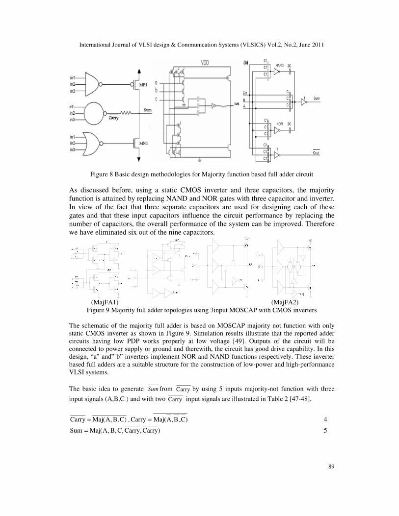
Figure 8 Basic design methodologies for Majority function based full adder circuit
As discussed before, using a static CMOS inverter and three capacitors, the majority
function is attained by replacing NAND and NOR gates with three capacitor and inverter.
In view of the fact that three separate capacitors are used for designing each of these
gates and that these input capacitors influence the circuit performance by replacing the
number of capacitors, the overall performance of the system can be improved. Therefore
we have eliminated six out of the nine capacitors.
(MajFA1) (MajFA2)
Figure 9 Majority full adder topologies using 3input MOSCAP with CMOS inverters
The schematic of the majority full adder is based on MOSCAP majority not function with only
static CMOS inverter as shown in Figure 9. Simulation results illustrate that the reported adder
circuits having low PDP works properly at low voltage [49]. Outputs of the circuit will be
connected to power supply or ground and therewith, the circuit has good drive capability. In this
design, “a” and” b” inverters implement NOR and NAND functions respectively. These inverter
based full adders are a suitable structure for the construction of low-power and high-performance
VLSI systems.
The basic idea to generate Sum from Carry by using 5 inputs majority-not function with three
input signals (A,B,C ) and with two Carry input signals are illustrated in Table 2 [47-48].
)C,B,A(MajCarry = , )C.,B,A(MajCarry = 4
)Carry,Carry,C,B,A(MajSum = 5

International Journal of VLSI design & Communication Systems (VLSICS) Vol.2, No.2, June 2011
90
The majority full adder design is implemented by means of majority function, based on CMOS
technology. This design is based on the idea that the carry output function is the same as 3- input
majority function shown in Figure 10.
Figure 10 Basic design approach for Majority Not function based full adder cell
5.1 Reported Majority Function Hybrid and Mixed mode Full Adder Topologies
As reported in HyFA1, hybrid full adder circuit of Figure 11(a) uses 16 transistors. Its output Sum
function is based on 5 input majority-not gates. In this design, the first majority-not gate is
implemented with a high-performance CMOS bridge circuit [48]. This design uses more
transistors, called bridge transistors, sharing transistors of different paths to generate new paths
from supply lines to circuit outputs. The bridge design style offers more regularity and higher
performance than the other CMOS design styles and is completely symmetric in structure. Using
the bridge circuit leads to reduction of delay and power consumption of the full adder cell and it
also increases the robustness of the circuit
Figure 11(a) HyFA1 (Majority Bridge) Figure 11(b) MixFA1 (Current mode Dynamic)
In MixFA1 mixed mode full adder circuit of Figure 11(b) uses 16 transistors. Its output Sum
function is based on Current mode majority function. In this design, the first majority-not gate is
implemented with a high-performance dynamic CMOS bridge circuit [48]. The advantage of this
adder cell is higher speed, lower transistor count and it compromises noise margin.
Maj.
Function
A
B
Carry
C
Maj.
Function
B
C
Sum
A

International Journal of VLSI design & Communication Systems (VLSICS) Vol.2, No.2, June 2011
91
5.2 Newly Design Hybrid Full Adder Topologies
Figure 12(a) Design 1(HyFA2) Figure 12(b) Design 2 (HyFA3)
The design1 HyFA2 uses 14 transistors and 3 input capacitors. Full adder output Carry function is
designed with 3 input Majority Not function logic and output Sum function generated in bridge
logic style as shown in Figure 12(a). In this design, the majority-not gate is implemented with a
capacitors and high-performance CMOS bridge circuit. The advantage of this adder cell is higher
speed, lower transistor count and it compromises noise margin. This type of circuit is preferred in
smaller area requirement with lesser delay at low voltage.
The design2 (HyFA3) uses 15 transistors and is based on dynamic CMOS structure. Full adder
output Carry function is designed with 3 input Majority Not function logic and output Sum
function generated in dynamic C-CMOS logic style as shown in Figure 12(b). The advantages of
the dynamic CMOS logic style are its robustness against voltage scaling and transistor sizing
(high noise margins) and thus reliable operation at low voltages and arbitrary (even minimal)
transistor sizes (ratio less logic) are possible. Input signals are connected to transistors gates only,
which facilitates the usage and characterization of logic cells.
Figure 13(a) Design 3 (HyFA4) Figure 13(b) Design 4 (HyFA5)
The design3 HyFA4 uses 16 transistors and is based on regular CMOS structure with pull-up and
pull-down transistors. Full adder output Carry function is designed in C-CMOS logic style and
output Sum function generated from 5 input Majority Not function logic as shown in Figure
13(a). The Pseudo nMOS based Majority-Function full adder design4 (HyFA5) operates on
pseudo logic, which is referred to ratioed style. Full adder output Carry function is designed in
Pseudo logic style and output Sum function generated from 5 input Majority Not function logic as
shown in Figure 13(b). This adder circuit uses 12 transistors to realize the negative addition
International Journal of VLSI design & Communication Systems (VLSICS) Vol.2, No.2, June 2011
92
function. In this circuit all the pMOS are replaced with a single pMOS and its gate is connected to
ground terminal. The advantage of this adder cell is higher speed, lower transistor count and it
compromises noise margin.
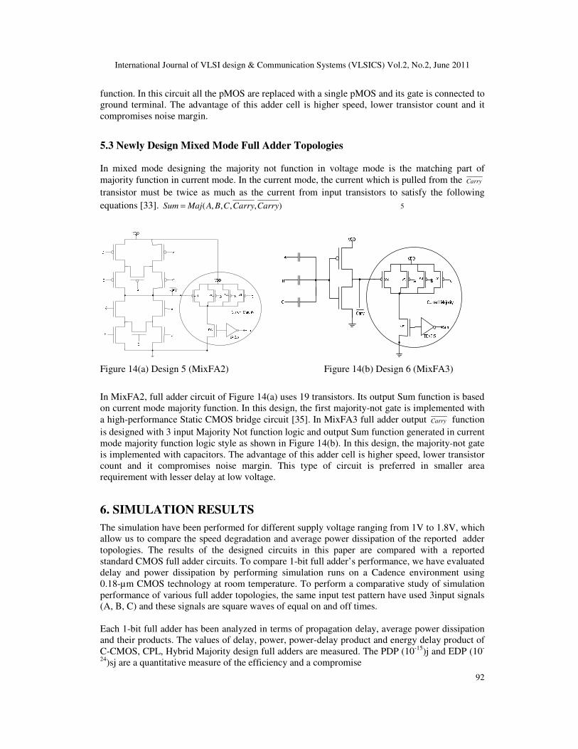
5.3 Newly Design Mixed Mode Full Adder Topologies
In mixed mode designing the majority not function in voltage mode is the matching part of
majority function in current mode. In the current mode, the current which is pulled from the Carry
transistor must be twice as much as the current from input transistors to satisfy the following
equations [33]. ),,,,( CarryCarryCBAMajSum = 5
Figure 14(a) Design 5 (MixFA2) Figure 14(b) Design 6 (MixFA3)
In MixFA2, full adder circuit of Figure 14(a) uses 19 transistors. Its output Sum function is based
on current mode majority function. In this design, the first majority-not gate is implemented with
a high-performance Static CMOS bridge circuit [35]. In MixFA3 full adder output Carry function
is designed with 3 input Majority Not function logic and output Sum function generated in current
mode majority function logic style as shown in Figure 14(b). In this design, the majority-not gate
is implemented with capacitors. The advantage of this adder cell is higher speed, lower transistor
count and it compromises noise margin. This type of circuit is preferred in smaller area
requirement with lesser delay at low voltage.
6. SIMULATION RESULTS
The simulation have been performed for different supply voltage ranging from 1V to 1.8V, which
allow us to compare the speed degradation and average power dissipation of the reported adder
topologies. The results of the designed circuits in this paper are compared with a reported
standard CMOS full adder circuits. To compare 1-bit full adder’s performance, we have evaluated
delay and power dissipation by performing simulation runs on a Cadence environment using
0.18-µm CMOS technology at room temperature. To perform a comparative study of simulation
performance of various full adder topologies, the same input test pattern have used 3input signals
(A, B, C) and these signals are square waves of equal on and off times.
Each 1-bit full adder has been analyzed in terms of propagation delay, average power dissipation
and their products. The values of delay, power, power-delay product and energy delay product of
C-CMOS, CPL, Hybrid Majority design full adders are measured. The PDP (10-15)j and EDP (10-
24)sj are a quantitative measure of the efficiency and a compromise
International Journal of VLSI design & Communication Systems (VLSICS) Vol.2, No.2, June 2011
93
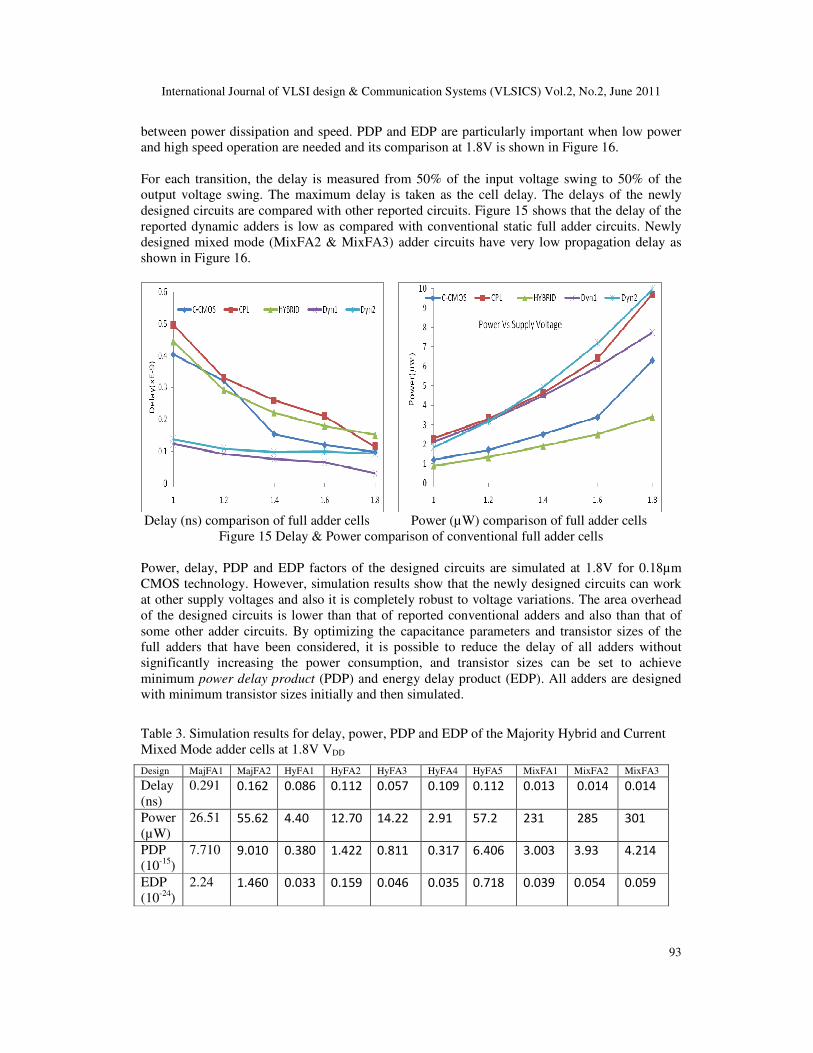
between power dissipation and speed. PDP and EDP are particularly important when low power
and high speed operation are needed and its comparison at 1.8V is shown in Figure 16.
For each transition, the delay is measured from 50% of the input voltage swing to 50% of the
output voltage swing. The maximum delay is taken as the cell delay. The delays of the newly
designed circuits are compared with other reported circuits. Figure 15 shows that the delay of the
reported dynamic adders is low as compared with conventional static full adder circuits. Newly
designed mixed mode (MixFA2 & MixFA3) adder circuits have very low propagation delay as
shown in Figure 16.
Delay (ns) comparison of full adder cells Power (µW) comparison of full adder cells
Figure 15 Delay & Power comparison of conventional full adder cells
Power, delay, PDP and EDP factors of the designed circuits are simulated at 1.8V for 0.18µm
CMOS technology. However, simulation results show that the newly designed circuits can work
at other supply voltages and also it is completely robust to voltage variations. The area overhead
of the designed circuits is lower than that of reported conventional adders and also than that of
some other adder circuits. By optimizing the capacitance parameters and transistor sizes of the
full adders that have been considered, it is possible to reduce the delay of all adders without
significantly increasing the power consumption, and transistor sizes can be set to achieve
minimum power delay product (PDP) and energy delay product (EDP). All adders are designed
with minimum transistor sizes initially and then simulated.
Table 3. Simulation results for delay, power, PDP and EDP of the Majority Hybrid and Current
Mixed Mode adder cells at 1.8V VDD
Design MajFA1 MajFA2 HyFA1 HyFA2 HyFA3 HyFA4 HyFA5 MixFA1 MixFA2 MixFA3
Delay
(ns)
0.291 0.162 0.086 0.112 0.057 0.109 0.112 0.013 0.014 0.014
Power
(µW)
26.51 55.62 4.40 12.70 14.22 2.91 57.2 231 285 301
PDP
(10-15
)
7.710 9.010 0.380 1.422 0.811 0.317 6.406 3.003 3.93 4.214
EDP
(10-24)
2.24 1.460 0.033 0.159 0.046 0.035 0.718 0.039 0.054 0.059

International Journal of VLSI design & Communication Systems (VLSICS) Vol.2, No.2, June 2011
94
Figure16 Delay and EDP of Hybrid and Mixed mode adder cells at 1.8V VDD
6.1. Results and Discussion
6.1.1. Average Power Comparison
In this section, we discuss the effect of supply voltage variation v/s. average power. In our
analysis the current mode full adders (MixFA1-MixFA3) are the most power consuming circuit at
1.8V due to constant current source. The power consumption worsens with the increase in the
voltage supply. Hybrid full adder HyFA4 has the lowest power consumption in comparison to the
other simulated adder circuits. It worked successfully at low voltage supply. The MixFA3 full
adder consumes higher power due to use of high power consuming current mode majority
function in a single unit.
6.1.2. Delay Comparison
Similar to previous simulation setup, the average propagation delay has been studied with the
supply voltage variation in all circuits. Simulation results in Figure 14 show that MajFA1 is the
best circuit in terms of speed at 1.8V VDD. It has high delay and high sensitivity against voltage
scaling. Design2 HyFA3 is the fastest full adder circuit. MixFA2 keeps a high distance from
design MixFA1 and shows better performance than MixFA3. Mixed mode adders have almost the
same delay at 1.8V.
6.1.3. Energy delay product (EDP) Comparison
Figure 16 shows the energy delay product of the Hybrid and mixed mode adder circuits. The
conditions are same as power and delay simulation setups. In low voltages, designed MixFA1 is
better than MixFA2 and new hybrid adders. Table 3 shows HyFA1 and HyFA4 have almost same
EDP. All the HyFA4 has better EDP than all new design circuits.
7. CONCLUSION
In this paper, we designed a new class of mixed mode logic family for CMOS technology. An
extensive performance analysis of 1-bit MOSCAP based hybrid majority function and current
mixed mode function full adders have been presented. Different adder logic styles have been
implemented, simulated, analyzed and compared. Using the adder categorization and hybrid-
CMOS design style, many full adders can be conceived. As an example, new full adders designed
using hybrid-majority function design style with C-CMOS, Bridge and Pseudo logic circuit are
presented in this paper that targets minimum delay and EDP. The characteristics of the newly

International Journal of VLSI design & Communication Systems (VLSICS) Vol.2, No.2, June 2011
95
designed adder circuits are compared against reported designed adders based on the worst case
delay, average power dissipation, power-delay product (PDP) and energy delay product (EDP).
The comparison of simulation results shows that the performance of the newly mixed mode
designs are superior in terms of high-speed as against other reference designs of full adder
circuits.
REFERENCES
[1] N. Weste and K. Eshraghian, (1993) Principles of CMOS VLSI Design: A System Perspective
Reading, MA: Addison –Wesley.
[2] John P. Uyemura, (2002) Introduction to VLSI circuits and systems, Wiley John & Sons, Inc.
[3] Sung-Mo Kang, Yusuf Leblebici, (2003) CMOS Digital Integrated Circuits: Analysis and Design,
TATA Mc GRAW-HILL.
[4] N. Weste and D. Harris, (2005) CMOS VLSI Design, Pearson Wesley.
[5] J. Uyemura, (1999) CMOS Logic Circuit Design, Kluwer.
[6] N. Jha and S. Gupta, (2003) Testing of Digital Systems. Cambridge, U.K.: Cambridge Univ. Press.
[7] J. M. Rabaey, A. Chandrakasan, B. Nikolic, (2002) “Digital Integrated Circuits, A design
Perspective,” 2nd Prentice Hall, Englewood Cliffs, NJ.
[8] R. Pedram and M. Pedram, (1996), Low Power Design Methodologies, Kluwer, Norwell, MA.
[9] N. Zhuang and H. Wu, (1992) A New Design of the CMOS full adder, IEEE J. Solid-State
Circuits, Vol. 27, No. 5, pp. 840–844.
[10] A. P. Chandrakasan and R.W. Brodersen, (1995) Low Power Digital CMOS Design, Kluwer
Academic Publishers.
[11] M.M Vai, (2001) VLSI Design, CRC Press, Boca Raton, FL.
[12] R.P. Brent and H. T. Kung, (1982) “A regular layout for parallel adders”, IEEE Trans. Computer,
Vol. 31, no. 3, pp. 260-264.
[13] T. Han and D.A.Carlson, (1987) “Fast area-efficient VLSI adders”, in Proc. 8th
IEEE Symp.
Computer Arithmetic, Italy, pp. 49-56.
[14] V.G. Oklobdzija, B.R. Zeydel, H.Q. Dao S. Mathew and R. Krishnamurthy, (2005) “Comparison
of high-performance VLSI adders in energy-delay space,” IEEE Trans. VLSI Syst., Vol. 13, No.
6, pp. 754-758.
[15] H.Q. Dao ,B.R. Zeydel and V.G. Oklobdzija, (2006) “Energy optimization of pipelined digital
system using circuit sizing and supply scaling,” IEEE Trans. VLSI Syst., Vol. 14, No. 2, pp. 122-
134.
[16] Uming Ko, PorasT.Balsara and Wai Lee, (1995) “Low-Power Design Techniques for High-
Performance CMOS Adders”, IEEE Trans. on very Large Scale Integration (VLSI) Systems, Vol.
3, No.2, pp. 327-333.
[17] S. Issam, A Khater, A. Bellaouar and M.I. Elmasry, (1996) “Circuit techniques for CMOS low
power high performance multipliers,” IEEE Journal Solid- State Circuits, Vol. 31, pp. 1535-1544.
[18] Reto Zimmermann and Wolfgang Fichtner, (1997) “Low-power Logic Styles: CMOS versus pass
transistor logic”, IEEE Journal of Solid-State Circuits, Vol. 32, No. 7, pp. 1079-1090.
[19] Mark Vesterbacka, (1999) “A 14-Transistor CMOS Full Adder With Full Voltage-Swing Nodes”,
Proc. IEEE Workshop Signal Processing Systems, pp. 713-722.
[20] R. Shalem, E. John and L. K. John (1999) “A NOVEL LOW POWER ENERGY RECOVERY
FULL ADDER CELL”, Proc. Great Lake Symp. VLSI, pp. 380–383.
International Journal of VLSI design & Communication Systems (VLSICS) Vol.2, No.2, June 2011
96
[21] D. Radhakrishnan, (2001) “Low-voltage low-power CMOS full adder”, Proc. Inst. Elect. Engg.
Circuits Devices Systems, Vol. 148, No. 1, pp. 19-24.
[22] Ahmed M. Shams, Tarek K. Darwish, and Magdy A. Bayoumi, (2002) “Performance Analysis of
Low-Power 1-Bit CMOS Full Adder Cells”, IEEE Trans. on Very Large Scale Integration (VLSI)
Systems, Vol. 10, No. 1, pp. 20–29.
[23] Hung Tien Bui, Yuke Wang and Yingtao Jiang, (2002) “Design and Analysis of Low-Power 10-
Transistor Full Adders Using Novel XOR-XNOR Gates,” IEEE Trans. on Circuits & Systems II:
Analog and Digital Signal Processing, Vol. 49, No. 1, pp. 25-30.
[24] S. Wairya, R. K. Nagaria and S. Tiwari, (2010) “A Novel CMOS Full Adder Topology for Low
Voltage VLSI Applications” International Conference on Emerging Trends in Signal Processing
& VLSI Design ‘SPVL2010’, Hyderabad, India, pp. 1142-1146.
[25] Y. Jiang, A. Alsheridah, Y. Wang, E. shah, and J. Chung, (2004) “A Novel Multiplexer-Based
Low Power Full Adder”, IEEE Trans. on Circuits and Systems, Vol. 51, No. 7.
[26] Fartash Vasefi and Z. Abid, (2005) “Low Power N-bit Adders and Multiplier Using Lowest
Number of Transistors 1- bit Adders”, IEEE conference proceeding of CCECE/CCGEI,
Saskatoon, pp.1731-1734.
[27] Chip-Hong Chang, Jiangmin Gu, Mingyan Zhang, (2005) “A Review of 0.18µm Full Adder
Performances for Tree Structured Arithmetic Circuits”, IEEE Trans. on Very Large Scale
Integration (VLSI) Systems, Vol. 13, No. 6, pp. 686-695.
[28] Jin-Fa-Lin, Yin-Tsung Hwang, Ming-Hwa Sheu, and Cheng- Che Ho, (2007) “A Novel High-
Speed and Energy Efficient 10-Transistor Full Adder Design", IEEE Trans. on Circuits and
Systems I, Vol. 54, No. 5, pp.1050-1059.
[29] Shiv Shankar Mishra, S.Wairya, R.K. Nagaria and S. Tiwari, (2009) “New Design Methodologies
for High Speed Low Power XOR-XNOR Circuits”, Journal of World Academy Science,
Engineering and Technology (WASET , Vol. 55, No. 35, pp. 200-206.
[30] Adarsh Kumar Agrawal, S.Wairya, R.K. Nagaria, S. Tiwari, (2009) “A New Mixed Gate
Diffusion Input Full Adder Topology for High Speed Low Power Digital Circuits”, World Appl.
Sci. J. (WASJ) 7 (Special Issue of Computer & IT): pp. 138-144.
[31] Sourabh Kamthey, T.N.Sharma, R.K.Nagaria, S. Wairya (2009) “A Novel Design for Testability
of Multiple Precharged Domino CMOS Circuits”, World Appl. Sci. J. (WASJ) 7 (Special Issue of
Computer & IT), pp. 175-181.
[32] Subodh Wairya, Rajendra Kumar Nagaria and Sudarshan Tiwari, (2011) “New Design
Methodologies for High-Speed Low-Voltage 1-Bit CMOS Full Adder Circuits”, Journal of
Computer Technology and Application (JCTA), Vol. 2, No. 3, pp. 190-198.
[33] Keivan Navi, Roshanak Zabihi, Majid Haghparast, Touraj Nikobin, (2008) “A Novel Mixed Mode
Current and Dynamic Voltage Full adder,” World Applied Sciences Journal, Vol.4, pp. 289 -294.
[34] Reza Faghih Mirzaee, Mohammad Hossein Moaiyeri, Keivan Navi, (2010) “High Speed NP-
CMOS and Multi-Output Dynamic Full Adder Cells,” International Journal of Electrical and
Electronics Engineering, Vol. 4, pp. 304-310.
[35] Rumi Zhang, Konrad Walus, Wei Wang and Graham A. Jullien, (2004) “A Method of Majority
Logic Reduction for Quantum Cellular Automata”, IEEE Trans. On Nanotechnology, Vol. 3, No.
4, pp. 443-450.
[36] Walid Ibrahim, Valeriu Beiu, and Mawahib Hussein Sulieman, (2008) “On the Reliability of
Majority Gates Full Adders”, IEEE Trans. On Nanotechnology, Vol. 7, No. 1, pp. 57-67.
[37] Keivan Navi, Omid Kavehei, Mahnoush Rouholamini, Amir Sahafi, Shima Mehrabi, (2007) “A
Novel CMOS Full Adder", 20th
International Conference on VLSI Design (VLSID'07), India, pp.
303-307.

International Journal of VLSI design & Communication Systems (VLSICS) Vol.2, No.2, June 2011
97
[38] Keivan Navi, Omid Kavehei, Mahnoush Rouholamini, Amir Sahafi, Shima Mehrabi and Nooshin.
Dadkhahi, (2008) “Low-Power and High-Performance 1-Bit CMOS Full-Adder Cell”, Journal of
Computers, Vol. 3, No. 2, pp. 48-54.
[39] Omid Kavehei, Mostafa Rahimi Azghadi, Keivan Navi and Amir-Pasha Mirbaha, (2008) “Design
of Robust and High –Performance 1-Bit CMOS Full Adder for Nanometer Design”, IEEE
Computer Society Annual Symposium VLSI (ISVLSI), Montpellier Fr., pp. 10-15.
[40] Keivan Navi and Neda Khandel, (2008) “The Design of a High-Performance Full Adder Cell by
Combining Common Digital Gates and Majority Function”, European Journal of Scientific
Research, Vol. 23, No.4, pp. 626-638.
[41] K. Navi, R. Faghih, M.H. Moaiyeri, B. Mazloom Nezhad, O. Hashemipour and K. Shams, (2008)
“Ultra high speed Full Adders”, IEICE Electronics Express, Vol. 5, No. 18, pp. 744-749.
[42] Keivan Navi, Mohammad Reza Saatchi and Omid Daei, (2009) “A High-Speed Hybrid Full
Adder”, European Journal of Scientific Research, Vol. 26, No.1, pp. 29-33.
[43] Keivan Navi, Mehrdad Maeen and O. Hashemipour, (2009) “An energy efficient full adder cell for
low voltage”, IEICE Electronics Express, Vol. 6, No. 9, pp. 553-559.
[44] Mehrdad Maeen, Vahid Foroutan and Keivan Navi, (2009) “On the design of low power 1-bit full
adder cell”, IEICE Electronics Express, Vol. 6, No. 16, pp. 1148-1154.
[45] Mohammad Hossein Moaiyeri, Reza Faghih Mirzaee, Keivan Navi and Tooraj Nikoubin, (2009)
“New high-performance majority function based Full Adders”, Proc. of 14th
International CSI
Computer Conference (CSICC 09), pp. 100-104.
[46] Mohammad Hossein Moaiyeri and Reza Faghih Mirzaee, (2009) “Two New Low-Power and
High-Performance Full Adders”, Journal of Computers, Vol. 4, No. 2, pp. 119-126.
[47] Keivan Navi, Mehrdad Maeen, Vahid Foroutan, Somayeh Timarchi and Omid Kavehei, (2009)
“A novel low power full-adder cell for low voltage”, INTEGRATION, the VLSI Journal, Vol. 42,
pp. 457-467.
[48] Keivan Navi, Mohammad Hossein Moaiyeri, Reza Faghih Mirzaee, Omid Hashemipour, Babak
Mazloom Nezhad, (2009) “Two new low-power Full Adders based on majority-not gates”,
Microelectronics Journal, Vol. 40, pp. 126-130.
[49] K. Navi, V. Foroutan, M. Rahimi, M. Maeen, M. Ebrahimpour, M. Kaveh, O. Kavehei, (2009) “A
novel low-power full-adder cell with new technique in designing logical gates based on static
CMOS inverter”, Microelectronics Journal, Vol. 40, pp. 1441-1448.
[50] Mojtabavi Naeini Mahshid and Navi Keivan, (2010) “A New Full-Adder Based on Majority
Function and Standard Gates”, Journal of Communication and Computer, Vol. 7, No. 5 pp. 1-7.
[51] M. Haghparast and K. Navi, (2007) “A Novel Reversible Full Adder Circuit for Nanotechnology
based system,” Journal of Applied Science, Vol. 7, pp. 3996-4000.
[52] Vahid Foroutan, Keivan Navi and Majid Haghparast, (2008) “A New Low Power Dynamic Full
Adder Cell Based on Majority Function,” World Applied Sciences Journal, Vol. 4, No. 1, pp. 133-
141.
[53] D. A. Freitas and K. W, (1987) “A CMOS Current Comparator Circuit,” Electronics Letters,
19(7), pp. 695-697, 1983.
[54] K. Navi, A. Kazeminejad and D. Etiemble, (1994) “Performance of CMOS Current Mode Full
Adders,” IEEE Proc. International Symp. , Multiple Valued Logic, pp. 27-34.
[55] A. Ghorbannia Delavar, K. Navi and O. Hashemipour, (2005) “Very Fast Current Mode Logic
Gates,” CSIT Conference, Yerevan, Armenia, pp. 19-23.
[56] K. Navi, M. Kazemi Parsa and A. Ghorbannia Delavar, (2005) “Very High Speed Current Mode
Logical Circuits,” CSI Journal of Computer Science and Engineering, spring, pp. 45-50.

International Journal of VLSI design & Communication Systems (VLSICS) Vol.2, No.2, June 2011
98
[57] A. Pishvaie, K. Navi and M. Haghparast, (2007) “Design Hybrid Logical Gates with Current and
Voltage output,” 12th
International CSI Computer Conference (CSICC), Persian, pp. 911-915.
[58] K. Navi, V. Foroutan, B. Mazloomnejad, Sh. Bahrololoumi, O. Hashemipour, M. Haghparast,
(2008) “A Six Transistors Full Adder,” World Applied Sciences Journal, Vol. 4, pp. 142-149.
Authors
Subodh Wairya is an Assistant Professor of Electronics Engineering department at the
Institute of Engineering & Technology, (IET) Lucknow, Uttar Pradesh, India. He did M.E.
(Telecommunication) from Jadavpur University, Kolkata and B.TECH (Electronics
Engineering.) from H.B.T.I., Kanpur, India. He has more than fifteen years experience in
academics. He has contributed research papers in National & International reputes. He has
also served as Scientist ‘B’ in Defence Research & Development Organization (DRDO)
and Graduate Engineer (Design Project) in Hindustan Aeronautical Limited (HAL),
Lucknow. He has been on several academic examination assignments for different
Universities. He is a life member for professional & Technical societies like ISTE
(LM33784), IETE (M189081L), Institute of Engineers (MIE M133861-1). Pursuing Ph.D
on “Performance Evaluation of High-Speed CMOS Circuit Designs” from Motilal Nehru
National Institute of Technology (M.N.N.I.T) Allahabad, India. Email:
Rajendra Kumar Nagaria is an Associate Professor of Electronics & Communication
Engineering at Motilal Nehru National Institute of Technology (MNNIT), Allahabad,
India. He received B.Tech. and M.Tech. in Electronics Engineering from Kamla Nehru
Institute of Technology (KNIT) Sultanpur, India and Ph.D. (Engg.) from Jadavpur
University, Kolkata, India. He has been over 22 years of teaching & research experience.
He has published more than forty research papers of National & International reputes. His
name is enlisted in an exclusive directory Marquis Who’s Who in the world. He is also
nominated for the award as International Educator of the year 2005, by International
Biographical Centre, Cambridge England. He is fellow of professional bodies like Institute
of Engineers (India) and Indian Society for Technical Education. He has guided the thesis
of many PG students and presently Six research scholars are working under his
supervision. His area of interest is Mixed-mode signal processing, High-Speed
networks/VLSI Design. Email: [email protected]
Sudarshan Tiwari received the B.Tech. degree in Electronics Engineering from I.T.BHU,
Varanasi, India in 1976, the M.Tech. degree in Communication Engineering from the same
institution in 1978 and PhD degree in Electronics and Computer Engineering from IIT
Roorkee, India in 1993. Presently, he is Professor and Head of Department of Electronics
and Communication Engineering. Motilal Nehru National Institute of Technology
(M.N.N.I.T), Allahabad, India. He has also worked as Dean Research and Consultancy of
the institute from June 2006 till June 2008. He has more than 28 years of teaching and
research experience in the area of communication engineering and networking. He has
supervised a number of M.Tech and PhD thesis. He has served on the program committee
of several seminars, workshops and conferences. He has worked as a reviewer for several
conferences and Journals both nationally and internationally. He has published over 100
research papers in different Journals and Conferences. He has served as a visiting
professor at Liverpool John Moore’s University, Liverpool, UK. He has completed several
research projects sponsored by government of India. He is a life member of Institution of
Engineers (India) and Indian society of Technical Education (India), he is a member of
Institution of Electrical and Electronics Engineers (USA). His current research interest
include, in the area of WDM optical networks, wireless ad hoc & sensor networks and next
generation networks. Email: [email protected].
![CHAPTER 5 THE ALLARD REGULARITY THEOREMmaths-proceedings.anu.edu.au/.../CMAProcVol3-Chapter5.pdfCHAPTER 5 THE ALLARD REGULARITY THEOREM Here we discuss Allard's ([AWl]) regularity](https://img.pdfslide.us/doc/110x75/5fb2cc5e95482068621741eb/chapter-5-the-allard-regularity-theoremmaths-chapter-5-the-allard-regularity-theorem.jpg)


![REGULARITY OF OPTIMAL TRANSPORT MAPS [after Ma{Trudinger ...afigalli/lecture-notes-pdf/Regularity-of... · REGULARITY OF OPTIMAL TRANSPORT MAPS [after Ma{Trudinger{Wang and Loeper]](https://img.pdfslide.us/doc/110x75/5f08d5757e708231d423f207/regularity-of-optimal-transport-maps-after-matrudinger-afigallilecture-notes-pdfregularity-of.jpg)


![T2 · 2019. 8. 1. · 310 M.N. MUKHERJEE AND S.P. SINHA regularity were also defined in [6]. Wecharacterize fuzzy regularity and these weaker forms of fuzzy regularity in terms of](https://img.pdfslide.us/doc/110x75/60b0546db5896d7af80bbfee/t2-2019-8-1-310-mn-mukherjee-and-sp-sinha-regularity-were-also-defined.jpg)