Embed Size (px)
Citation preview

New Approach to Distinguish CopperMolten Marks Based on QuantitativeMicrostructure Analysis Using ElectronBackscatter Diffraction
Jinyoung Park , Safety Research Department, Korea Electrical SafetyCorporation Research Institute, 111, Anjeon-ro, Iseo-myeon, Wanju-gun,Jeollabuk-do 55365, Republic of Korea
Joo-Hee Kang *, Materials Analysis & Evaluation Department, KoreaInstitute of Materials Science, 797, Changwon-daero, Seongsan-gu,Changwon-si, Gyeongsangnam-do 51508, Republic of Korea
Eui Pyeong Lee , Department of Fire Safety Engineering, Jeonju University,303, Cheonjam-ro, Wansan-gu, Jeonju-si, Jeollabuk-do 55069, Republic ofKorea
Young Ho Ko , Department of Electrical Engineering, Jeonbuk NationalUniversity, 567, Baekje-daero, Deokjin-gu, Jeonju-si, Jeollabuk-do 54896,Republic of Korea
Sun Bae Bang , Safety Research Department, Korea Electrical SafetyCorporation Research Institute, 111, Anjeon-ro, Iseo-myeon, Wanju-gun,Jeollabuk-do 55365, Republic of Korea
Received: 23 May 2020/Accepted: 27 November 2020/Published online: 11 January 2021
Abstract. Molten marks identified at a fire site can aid in determining the cause of a
fire. Quantitative analysis of such molten marks has not yet been reported, despiteseveral identification methods for molten marks being proposed based on opticalmicrographs. Herein, we propose a new methodology to establish the quantitativemicrostructure parameters of the molten marks using electron backscatter diffraction
(EBSD). The globules were generated by heating the copper conductor to 1100�C ina non-energized state. Then, the arc beads were prepared by shorting the copper wireat 25�C and 900�C in an energized state. The globules did not show evident demarca-
tion lines and indicated that the microstructure consisted of globular or dendriticgrains; this demonstrated that their characteristics were distinctly different from thoseof arc beads. However, the primary arc beads (PABs) shorted at 25�C exhibited a
strong (001) texture perpendicular to the demarcation line and comprised large frac-tions of columnar grains with a small grain aspect ratio (GAR). The microstructureof secondary arc beads (SABs) shorted at 900�C presented a mixture of elongatedand equiaxed grains with a large GAR and no specific development of texture. The
GAR and (001) fraction perpendicular to the demarcation line could be discriminant
*Correspondence should be addressed to: ; Joo-Hee Kang, E-mail: [email protected]
Fire Technology, 57, 1667–1682, 2021
� 2021 The Author(s)
Manufactured in The United States
https://doi.org/10.1007/s10694-020-01076-9
1

parameters of PABs and SABs. Consequently, EBSD methods can be newly applied
for the classification of globules, PABs, and SABs based on the quantitativemicrostructure information and orientation distribution.
Keywords: Copper, Molten mark, Globule, Arc bead, Electron backscatter diffraction (EBSD), Mi-
crostructure
1. Introduction
Molten marks refer to rounded masses of melted copper. Molten marks are classi-fied into two categories [1, 2]: globules melted by fire and the arc beads melted byelectrical energy. Arc beads can be further divided into primary arc beads (PABs)and secondary arc beads (SABs). Globules are molten marks formed at high tem-peratures above the melting point (1083�C) of copper in a non-energized state.Arc beads are molten marks formed when a significant short-circuit current surgesthrough an electrical wire. PABs are molten marks resulting from the initial shortcircuit that acts as a source of ignition. SABs are molten marks formed due to ashort circuit that occurred in an energized state after the wire insulation had beenburned off by the flames. Therefore, the molten marks identified at a fire site canaid in determining the cause of the fire.
Molten marks can be predicted to exhibit different solidification behavioraccording to the ambient temperature, heat transfer, and Joule heat. This isbecause ambient temperature causes changes in the solidification parameters suchas temperature gradient and cooling rate. These changes eventually affect themicrostructure, such as the grain size and shape, in the molten marks. Severalclassification methods for molten marks have been proposed, and metallographicstudies have been actively conducted to analyze microstructure distinctions usingthe optical microscope [3–7]. Though the analysis of optical micrographs is amore scientific method than the observation of the appearance, it is difficult toderive quantitative discriminant parameters because optical microscopes have alimitation of resolution and cannot analyze crystallographic orientations ofmicrostructures. To observe fine grains with sizes under several tens of microns,proficient researchers and proper etching conditions are integral. An automaticorientation mapping system based on the scanning electron microscope (SEM)was developed in the late 1990s, called electron backscatter diffraction (EBSD) [8].EBSD measurement is widely used for micro-scale microstructure and crystallo-graphic features, and quantitative microstructure analysis is possible from pixe-lated orientation information. In this study, using these advantages of EBSD, wepropose a new method for quantitatively classifying molten marks. To this end,EBSD analysis of molten marks was performed and microstructure parameterswere deduced to distinguish among globules, PABs, and SABs. It should be notedthat this study is applicable to the limited conditions of bare wires contacting withdirect flame. Other cases such as the insulated wiring exposed to thermal radiationin a compartment fire are beyond the scope of the study.
For the deduction of quantitative discriminant parameters, non-energized cop-per wires were melted at 1100�C to generate globules, and energized wires were
1668 Fire Technology 2021

short-circuited at room temperature (25�C) and high temperature (900�C) to cre-ate PABs and SABs; the terms ‘‘PAB’’ and ‘‘SAB’’ used herein are limited to arcbeads generated at 25 and 900�C, respectively. This study employed an EBSDtechnique to distinguish the molten marks based on the microstructure such asgrain size, shape, and local orientation distribution; quantitative parameters weresuggested to distinguish among globules, PABs, and SABs.
2. Materials and Methods
In order to generate globules, the wire was fixed to the holder in a non-energizedstate, and the ambient temperature was raised to 1100�C. The globules wereformed after approximately 20 s from flame initiation. PABs were prepared byforming a short-circuit at room temperature (25�C) without using a gas burner.SABs were fabricated by forming a short-circuit after increasing the temperatureto 900�C and holding for 2 min. After the short-circuit, the temperature wasmaintained for an additional 2 min. This method was referred to in the report byWeinschenk et al. [9], wherein an overcurrent fault or grounding fault occurred atapproximately 900�C within 2 min on average after the flashover. Figure 1 showsa detailed experimental setup for preparing PABs and SABs. The test wires werefixed to both holders, and the left wire was slowly moved using the movementcontrol device for the two wires to make contact with each other. The reason foradopting this method is to maintain the exposure time to the external flame andallow data to be obtained under fixed conditions. A gas burner (propane gas) wasalso installed at the bottom of the short-circuit point. The controller was used toadjust the size of the flame up to 2 cm in diameter and up to 10 cm in height, andits maximum temperature up to 1300�C (tolerance temperature: ± 50�C).
Depending on the magnitude of the short-circuit current, the amount of heatgenerated at the short-circuit point may affect the size and shape of the moltenmark. Accordingly, a short-circuit limit device was manufactured by referring tothe point contact arc test current according to the rated voltage of UL1699 [10].This was done to obtain molten marks of similar size and shape. The short-circuitcurrent was limited to a maximum of 500 A at a rated voltage of 220 V. A 220 VAC power source was used in the experiment with a frequency of 60 Hz. A mol-ded case circuit breaker (MCCB) was used to protect the power system from
Figure 1. Schematic illustration of the short-circuit generator.
New Approach to Distinguish Copper Molten Marks Based on… 1669

forming a short-circuit. The MCCB, with a current rating of 30 A and an inter-rupting rating of 2.5 kA, was of the thermal and magnetic (TM) type. It wasoperated within 2 cycles with an overcurrent of 450 A or more.
The heat transfer condition was confirmed using K-type thermocouples by mea-suring the ambient temperature and the temperature of the copper conductor. Theconductors were bare copper wires with a diameter of 1.6 mm, and K-type ther-mocouples (temperature range: - 230 to 1250�C, limits of error: ± 2.2�C) werewelded to a copper conductor to measure the temperature, as shown in Fig. 2.Three thermocouples were attached at the short-circuit point (point A) and copperconductor (points B and C). Positions A, B, and C were at 30-mm intervals. Tem-perature profiles were monitored for 3 min from flame initiation when the ambienttemperature (point T in Fig. 2) was set to 900�C, which was the same conditionused for SAB generation. The ambient temperature was measured simultaneouslyat a position 2-mm away from the short-circuit point (point A) in the horizontaldirection.
Specimen preparation for EBSD is critical because diffracted electrons appearabove 10–50 nm on the surface. The presence of contaminants, oxidation, andmechanical damage on the surface hinders the incidence of electrons onto thespecimen. The flatness of the sample is necessary to ensure that the diffracted pat-terns are not obscured in a highly tilted sample. For this purpose, the moltenmark shown in Fig. 3a was hot-mounted using conductive resin and then wet-ground with SiC papers and polished with diamond suspensions and colloidal sil-ica suspensions (Fig. 3b). The sample preparation of copper and its alloys forEBSD analysis was introduced elsewhere [11, 12].
Field-emission scanning electron microscopes (FE-SEMs: Hitachi SU-70, Hita-chi SU-6600, JEOL JSM-7900F) equipped with EBSD systems (EDAX Hikari,Oxford Instruments Symmetry) were used to measure the orientation of the speci-mens. The accelerating voltage of the FE-SEM was set to 15 or 20 kV, and theprobe current was set to 15 nA. Mapping with a step size of 4 lm was performed.
Figure 2. Ambient and copper conductor temperature measurementconfiguration.
1670 Fire Technology 2021

The orientation varied significantly according to the direction of the specimenon the holder, especially when using EBSD to measure the orientation. The speci-men refers to a molten mark secured to a flat cross-section through mounting andpolishing. Accordingly, completely different orientation results can be obtaineddepending on how the specimen coordinate system is set, indicating that the refer-ence coordinate of the molten mark should be clearly selected. The demarcationline between the unmelted and the melted zones in the molten mark was formedby the short circuit [2, 13]. Accordingly, the demarcation line can be set as the ref-erence point of the specimen coordinate system. The specimen coordinate axiswere set to the longitudinal direction (LD), perpendicular to the demarcation line.
Post-processing of EBSD results was performed using EDAX TSL OIM 7.3software. The grain was set such that the minimum grain size was 2 pixels, andthe tolerance angle was 5�. Grain confidence index (CI) standardization andneighbor orientation correlation were adopted, including a tolerance angle of 5�for the clean-up. The mounting resin sand pores inside the molten marks wereremoved during post-processing.
3. Experimental Results and Discussion
Figure 4 shows the temperature change of the ambient temperature (point T) andthe copper conductor temperature (points A, B, and C) with respect to the pas-sage of time from flame initiation. The ambient temperature was measured 2 mmaway from the short-circuit point. The ambient temperature reached 900�C after42.2 s from flame initiation and the temperature at A followed that of point Twith a small difference. The average temperatures at T and A after 42.2 s were910 and 888�C, respectively, and the difference between them was 22�C. Thisresult was due to the heat conduction from A to C, and the temperature differ-ence between A and C was approximately 687�C, which resulted in the release ofa significant amount of heat. The graph in Fig. 4 shows that the temperature atthe high temperature region of T and A fluctuates significantly, while it is rela-
Figure 3. a Appearance of molten mark and b cross-section of themolten mark after mounting and polishing.
New Approach to Distinguish Copper Molten Marks Based on… 1671

tively stable at points B and C. However, the minimum arc temperature isapproximately 6000 K when a short circuit occurs [14]; the temperature differencebetween T and A can therefore be considered to be negligible. Therefore, it isdetermined that the measured ambient temperature at T can be replaced with thetemperature of the copper conductor at the short-circuit point A.
Figure 4. Temperature profiles of ambient temperature andtemperature of copper conductor at points A, B, and C.
Figure 5. The appearance of globules and beads: a globules, b PABs,and c SABs.
1672 Fire Technology 2021

Figure 5 shows the appearances of the globules and arc beads generated by theexperiment. The globules exhibited an unclear demarcation line between theunmelted and the melted zone, and gradual necking (Fig. 5a). In contrast, the arcbeads demonstrated a clear demarcation line and re-solidification waves and draw-ing lines appeared on the conductor surfaces as indicated in Fig. 5b, c. The glob-ules and beads produced during the experiment show no significant difference inappearance from the molten marks generated in an actual fire [13, 15].
LD orientation maps measured by EBSD are shown in Fig. 6. The color in theorientation maps indicates the orientation parallel to the LD, which is a perpen-dicular demarcation line according to the color key (Fig. 6a). The microstructureof the globules comprised globular or dendritic grains and a clear demarcationline was not observed in the gradual neck. Contrastingly, the arc beads in Fig. 6b,c exhibit outstanding demarcation lines depicted using white dotted lines. Simi-larly, the demarcation lines are shown from an external appearance in Fig. 5b, c.Therefore, globules could be distinguished clearly from the appearance andmicrostructure observed by the optical microscopes and EBSD analysis [2, 16, 17].Globules were prepared by exposure to higher temperatures than arc beads andconsequently, grain growth was instigated in a neck. Figure 6 shows that the aver-age grain size in the globule’s neck was larger than that of arc beads. Since drawnand annealed copper wires have strong (111) fiber textures along the LD [18, 19],weak (111) fiber texture near globules’ neck remained even after high temperatureexposure.
Figure 6. The orientation map of globules and beads: a globules andcolor key (upper side), b PABs, and c SABs. Demarcation lines areindicated by white dotted lines.
New Approach to Distinguish Copper Molten Marks Based on… 1673

Roby et al. [20] reported that the demarcation line became unclear when meltedand solidified again by an external flame after forming an arc bead. In addition,the arc beads can form without any direct flame impingement or convective heattransfer when insulated wire is exposed to thermal radiation. Novak et al. [21]presented that the arc beads formed in the radiant heat of 26–55 kW/m2. Mean-while the heat flux increased up to 140 kW/m2 in a short-circuit by the directflame [9]. The different heat flux can change the microstructure of molten marks.The arc beads formed by remelting or thermal radiation were not consideredbecause the deduction of distinguishable factors of molten marks, categorized asglobules, PABs, and SABs, is the main purpose of this study.
Figures 7 and 8 show the LD orientation maps, the crystal direction maps, andpole figures (PFs) for respective representative three specimens in PABs and SABs.In order to exclude the influence of wire texture in the necks, the pixels outside ofthe molten marks were removed for EBSD analysis in PABs and SABs. Fromhere, EBSD data of only molten marks was considered. The crystal directionmaps indicated the (001) component parallel to the LD with a tolerance angle of15�, with red parts belonging to (001)//LD. The (001), (011), and (111) PFs wereconsidered for precise texture analysis. The LD in PFs is normal to figures.
As shown in Fig. 7, the thermal gradient in the PABs was the steepest in thedirection perpendicular to the demarcation line because of the large temperaturedifference between the unmelted wire and the melted bead [22]. Therefore, the LDbecame the preferred growth direction of the columnar grains. In cubic material,including copper, the preferred solidification growth direction is known as the[001] direction [8]. The columnar grains with (001)//LD developed at the arc bead,as shown in the LD orientation map of Fig. 7. Although the small grains thatnucleated near the demarcation line have a relatively diverse orientation distribu-tion, a large number of columnar grains with a high growth rate occupied most ofthe PABs. The average area fraction occupied by the (001)//LD component for 10specimens was 65.4%.
In this study, the reference axis of PF was established by assuming that the LDis the central axis of a cylindrical coordinate, and the arc bead was formed in anaxisymmetric shape. PF is a method of displaying a crystal plane in the form ofdots or contours on a stereo projection to know the crystallographic orientationsbased on the set specimen coordinate axis. The crystal orientation distribution ofthe entire arc bead can be expressed as a density contour [8]. The intensity of thedensity contour was calculated using a series expansion of generalized sphericalharmonics. As mentioned above, it could be deduced that the (001)//LD texturedeveloped in the PFs as well as in the LD orientation map and crystal orientationmap.
It is noteworthy that the (001) fiber texture (PFs in Fig. 7a), or (rotated) cubetexture (PFs in Fig. 7b, c) formed in PABs. Here, it was assumed that the arcbeads are symmetrical to the shape and that the heat pass has axial symmetry inthe reference axis of the LD. However, the actual PABs were not perfectly spheri-cal and were not exactly symmetric to the LD. The reason is that the boundaryconditions of external parameters such as the melt flow, temperature gradient, andheat dissipation (radiation), change the microstructure during the solidification.
1674 Fire Technology 2021

Figure 7. The LD orientation maps, the crystal direction maps of(001)//LD (tolerance angle = 15�) and PFs of PABs: a–c show strongtexture of (001)//LD.
New Approach to Distinguish Copper Molten Marks Based on… 1675

Figure 8. The LD orientation maps, the crystal direction maps of(001)//LD (tolerance angle = 15�), and PFs of SABs: a–c show theweakening of (001)//LD component.
1676 Fire Technology 2021
Therefore, the development of a specific texture or the growth of columnar grainsthat deviate from (001)//LD needs to be clarified with respect to microstructureand texture evolution through further research using mesoscale modeling. TheEBSD results confirmed that (001)//LD columnar grains were strongly developedin PABs.
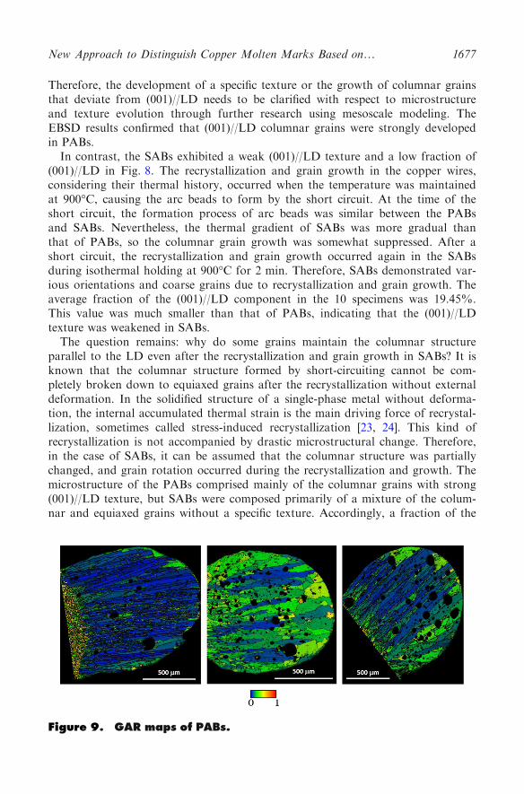
In contrast, the SABs exhibited a weak (001)//LD texture and a low fraction of(001)//LD in Fig. 8. The recrystallization and grain growth in the copper wires,considering their thermal history, occurred when the temperature was maintainedat 900�C, causing the arc beads to form by the short circuit. At the time of theshort circuit, the formation process of arc beads was similar between the PABsand SABs. Nevertheless, the thermal gradient of SABs was more gradual thanthat of PABs, so the columnar grain growth was somewhat suppressed. After ashort circuit, the recrystallization and grain growth occurred again in the SABsduring isothermal holding at 900�C for 2 min. Therefore, SABs demonstrated var-ious orientations and coarse grains due to recrystallization and grain growth. Theaverage fraction of the (001)//LD component in the 10 specimens was 19.45%.This value was much smaller than that of PABs, indicating that the (001)//LDtexture was weakened in SABs.
The question remains: why do some grains maintain the columnar structureparallel to the LD even after the recrystallization and grain growth in SABs? It isknown that the columnar structure formed by short-circuiting cannot be com-pletely broken down to equiaxed grains after the recrystallization without externaldeformation. In the solidified structure of a single-phase metal without deforma-tion, the internal accumulated thermal strain is the main driving force of recrystal-lization, sometimes called stress-induced recrystallization [23, 24]. This kind ofrecrystallization is not accompanied by drastic microstructural change. Therefore,in the case of SABs, it can be assumed that the columnar structure was partiallychanged, and grain rotation occurred during the recrystallization and growth. Themicrostructure of the PABs comprised mainly of the columnar grains with strong(001)//LD texture, but SABs were composed primarily of a mixture of the colum-nar and equiaxed grains without a specific texture. Accordingly, a fraction of the
Figure 9. GAR maps of PABs.
New Approach to Distinguish Copper Molten Marks Based on… 1677

(001)//LD component can be selected as a factor to discriminate between PABsand SABs.
Figures 9 and 10 show the grain aspect ratio (GAR) maps of PABs and SABs,respectively. The GAR is given by the length of the minor axis divided by thelength of the major axis of an ellipse fit to grain [25]. The GAR varies fromapproaching zero for a very elongated particle, such as a grain in a cold-workedmetal and columnar structure, to near unity for an equiaxed grain. In the PABs,small grains were nucleated at the demarcation line, while the columnar grainsgrew parallel to the LD inside the molten marks. Therefore, the PABs consisted ofmostly columnar grains with small GARs, with 10 specimens having an averageGAR of 0.1327. In SABs, the grains that formed at the demarcation line weresmall, but the grains became larger when at a distance from the demarcation line.The columnar and equiaxed grains were mixed in SABs, and their GAR was lar-ger than that of PABs. The average GAR of 10 specimens was 0.2832 in SABs.The small grains were visible on the surface of the molten marks in PABs andSABs, which were observed as nucleated grains in the 1-lm-thick oxide layer(Cu2O) formed at high temperatures on the surface [26]. As described earlier, thecolumnar grains grown in the (001) direction preferentially occupied most of thePABs due to a steep thermal gradient. However, in SABs, the columnar andequiaxed grains were mixed because the (001)//LD texture was weakened byrecrystallization and grain growth. For this reason, the grain shape of PABs andSABs were different. Therefore, since the differences between the microstructuresof PABs and SABs were proved metallographically, it is possible to select GAR asa quantitative factor to discriminate between the PABs and SABs.
Based on the experimental results, the GAR and fraction of (001)//LD wereselected as factors to quantitatively discriminate between PABs and SABs, asshown in Fig. 11. The discriminant line (dotted line) was shown on the graphusing linear discriminant analysis (LDA) [27, 28] and the classification for thePABs (bottom right) and SABs (top left) can be applicable based on the GARand fraction of (001)//LD. Nevertheless, one should note that this discriminant
Figure 10. GAR maps of SABs.
1678 Fire Technology 2021

methodology is limited to molten marks produced at 25 and 900�C using a barewire diameter of 1.6 mm. Further studies should be conducted to analyze moltenmarks formed at different temperatures, wire diameters, and insulators. It isexpected that more data under various conditions can provide precise discriminantguidelines. Notably, this study shows the possibility of quantitative discriminationof molten marks based on the microstructure characteristics and orientation distri-bution using EBSD analysis.
4. Conclusion
In this study, we used EBSD analysis to quantitatively identify copper moltenmarks. The crystal orientation information of the globules and arc beads (PABs,SABs) was obtained and the characteristics of the microstructure were analyzed todeduce the discriminant parameters. The results can be summarized as follows:
� The globules exhibited gradual necking in appearance and indistinct demarca-tion lines in the EBSD results. However, the arc beads demonstrated apparentdemarcation lines which were caused by rapid microstructural change.
� The microstructure of PABs had most of their columnar grains parallel to theLD (perpendicular to the demarcation line). In the orientation distribution, the(001)//LD texture was highly developed while the GAR was small becausecolumnar grains primarily appeared.
� The microstructures of SABs consisted of a mixture of columnar and equiaxedgrains due to recrystallization and grain growth after the short-circuit. The(001)//LD texture was weak, and the GAR was larger than the values forPABs.
� Based on the experimental results, the discriminant function was presentedusing the fraction of (001)//LD and the GAR. The discriminant factors were
Figure 11. PAB and SAB distribution according to the fraction of(001)//LD and GAR.
New Approach to Distinguish Copper Molten Marks Based on… 1679

derived from the distribution of the GAR and the fraction of (001)//LD inPABs and SABs.
In conclusion, the possibility of quantitative discrimination of molten markswas confirmed by analyzing the microstructure and orientation distribution usingEBSD. Since this study was limited to bare copper wire (diameter 1.6 mm), it can-not be applied to all molten mark analysis. However, we hope that this study pro-vided an opportunity to lay the foundation for further quantitative analysis ofmolten marks. In the future, we plan to expand the range of molten marks thatcan be analyzed by conducting experiments under various environmental condi-tions.
5. Availability of Data and Material
The data related to this work can be obtained from the corresponding authorupon reasonable request.
Acknowledgments
This work was supported by the Fundamental Research Program grant funded bythe Korea Electrical Safety Corporation (KESCO) (No. 2019-0101). J.-H. Kangwas supported by the Fundamental Research Program of the Korea Institute ofMaterials Science (KIMS) (Grant No. PNK7070).
Author Contributions
All authors contributed to the study conception and design. Material preparation,data collection, and analysis were performed by JP, J-HK, EPL, YHK, and SBB.The manuscript was written and revised by JP and J-HK, and all authors com-mented and advised on the manuscript. All authors read and approved the finalmanuscript.
Funding
Korea Electrical Safety Corporation (KESCO) (No. 2019-0101), Korea Instituteof Materials Science (KIMS) (Grant No. PNK7070).
Code Availability
Not applicable.
Compliance with Ethical Standards
1680 Fire Technology 2021

Conflict of interest The authors declare neither a conflict of interest norcompeting interests.
Open Access
This article is licensed under a Creative Commons Attribution 4.0 InternationalLicense, which permits use, sharing, adaptation, distribution and reproduction inany medium or format, as long as you give appropriate credit to the originalauthor(s) and the source, provide a link to the Creative Commons licence, andindicate if changes were made. The images or other third party material in thisarticle are included in the article’s Creative Commons licence, unless indicatedotherwise in a credit line to the material. If material is not included in the article’sCreative Commons licence and your intended use is not permitted by statutoryregulation or exceeds the permitted use, you will need to obtain permissiondirectly from the copyright holder. To view a copy of this licence, visit http://creativecommons.org/licenses/by/4.0/.
References
1. Liu K-H, Shih Y-H, Chen G-J, Chou J-M (2015) Microstructural study on moltenmarks of fire-causing copper wires. Materials 8(6):3776–3790. https://doi.org/10.3390/ma8063776
2. Wright SA, Loud JD, Blanchard RA (2015) Globules and beads: what do they indicateabout small-diameter copper conductors that have been through a fire. Fire Technol51:1051–1070. https://doi.org/10.1007/s10694-014-0455-9
3. Levinson DW (1977) Copper metallurgy as a diagnostic tool for analysis of the originof building fires. Fire Technol 13:211–222. https://doi.org/10.1007/BF02303416
4. Wang L, Yao H-W, Wu Z-X, Liang D (2014) The application of image processing inthe electrical fire physical evidence identification. Procedia Eng 71:57–67. https://
doi.org/10.1016/j.proeng.2014.04.0085. Gao A, Zhao C-Z, Di M, Gao W, Zhang M, Xia D-W (2011) Microscopic investiga-
tion of a copper molten mark by optical microscopy (OM) and atomic force micro-
scopy (AFM). Procedia Eng 11:100–106. https://doi.org/10.1016/j.proeng.2011.04.6336. Zhang J-Z, Deng L (2013) Metallographic microcosmic analysis on primary short cir-
cuited melted bead of copper wire heated in different temperature. Procedia Eng
52:583–587. https://doi.org/10.1016/j.proeng.2013.02.1897. Lee EP, Ohtani H, Seki T, Hasegawa H, Imada S, Yashiro I (2000) Study on discrimi-
nation between primary and secondary molten marks by DAS. Bull Jpn Assoc Fire SciEng 50(1):1–12. https://doi.org/10.11196/kasai.50.1_1
8. Randle V, Engler O (2000) Introduction to texture analysis: Macrotexture, microtextureand orientation mapping. CRC Press, Florida
9. Weinschenk C, Madrzykowski D, Courtney P (2019) Impact of flashover fire conditions
on exposed energized electrical cords/cables. Fire Technol 56:959–991. https://doi.org/10.1007/s10694-019-00915-8
10. UL 1699 (2019) Standard for arc-fault circuit-interrupters. https://standardscatalog.ul.c
om/standards/en/standard_1699_3. Accessed 28 Apr 202011. Samuels LE (2003) Metallographic polishing by mechanical methods, 4th edn. ASM
International, Ohio
New Approach to Distinguish Copper Molten Marks Based on… 1681

12. Kang J-H, Kim SH (2010) Sample preparation for EBSD analysis: tip for metal withdelicate surfaces. Korean J Met Mater 48(8):730–740. https://doi.org/10.3365/KJMM.2010.48.08.730
13. National Fire Protection Association (2017) NFPA 921: guide for fire and explosioninvestigations 2017 edition. National Fire Protection Association. https://catalog.nfpa.org/NFPA-921-Guide-for-Fire-and-Explosion-Investigations-P1386.aspx?icid=D737.Accessed 16 July 2019
14. Babrauskas V (2003) Ignition handbook: principle and applications to fire safety engi-neering, fire investigation, risk management and forensic science. Fire Science Publish-ers, Issaquah
15. Cameron N (2020) A methodology for the identification and interpretation of damageon electrical wiring. Fire Arson Investig 71(1):22–30
16. Ettling BV (1987) Electrical wiring in building fires. Fire Technol 14:317–325. https://
doi.org/10.1007/BF0199839117. Wei M-M, Zhao Z, Liang D (2011) Experiment of electrical fire burned copper wire
and parameters analysis on metallographic test of melted mark. Procedia Eng 11:496–503. https://doi.org/10.1016/j.proeng.2011.04.688
18. Baudin T, Etter AL, Penelle R (2007) Annealing twin formation and recrystallizationstudy of cold-drawn copper wires from EBSD measurements. Mater Charact58(10):947–952. https://doi.org/10.1016/j.matchar.2006.09.009
19. Jakani S, Baudin T, de Novion C-H, Mathon M-H (2007) Effect of impurities on therecrystallization texture in commercially pure copper-ETP wire. Mater Sci Eng A456(1–2):261–269. https://doi.org/10.1016/j.msea.2006.11.137
20. Roby RJ, McAllister J (2012) Forensic investigation techniques for inspecting electricalconductors involved in fire. Award No. 2010-DN-BX-K246 report for the US Depart-ment of Justice. https://www.ncjrs.gov/pdffiles1/nij/grants/239052.pdf. Accessed 24 Nov2020
21. Novak CJ, Stoliarov SI, Keller MR, Quintiere JG (2013) An analysis of heat fluxinduced arc formation in residential electrical cable. Fire Saf J 55:61–68. https://doi.org/10.1016/j.firesaf.2012.10.007
22. Dantzig JA, Rappaz M (2016) Solidification, 2nd edn. EPFL Press23. Zhang T, Liu F, Wang HF, Yang GC (2010) Grain refinement in highly undercooled
solidification of Ni85Cu15 alloy melt: Direct evidence for recrystallization mechanism.
Scr Mater 63(1):43–46. https://doi.org/10.1016/j.scriptamat.2010.03.00624. Feng L, Gencang Y (2001) Stress-induced recrystallization mechanism for grain refine-
ment in highly undercooled superalloy. J Cryst Growth 231(1–2):295–305. https://doi.org/10.1016/S0022-0248(01)01438-5
25. EDAX (2017) TSL OIM analysis 7.3 manual. AMETEK EDAX26. Liu KH, Shih YH, Chen GJ, Chou JM (2015) Microstructural study on oxygen perme-
ated arc beads. J Nanomater . https://doi.org/10.1155/2015/373861
27. Kuhn M, Johnson K (2013) Applied predictive modeling. Springer, New York28. OriginLab (2020) Interpreting results of discriminant analysis. OriginLab Corporation.
https://www.originlab.com/doc/Origin-Help/DiscAnalysis-Result. Accessed 25 Mar 2020
Publisher’s Note Springer Nature remains neutral with regard to jurisdictional claims in published
maps and institutional affiliations.
1682 Fire Technology 2021