Embed Size (px)
Citation preview
IPSJ Transactions on System LSI Design Methodology Vol.12 53–64 (Aug. 2019)
[DOI: 10.2197/ipsjtsldm.12.53]
Invited Paper
Neuromorphic Computing Systems: From CMOS ToEmerging Nonvolatile Memory
Chaofei Yang1,a) Ximing Qiao1,b) Yiran Chen1,c)
Received: April 21, 2019
Abstract: The end of Moore’s Law and von Neumann bottleneck motivate researchers to seek alternative architec-tures that can fulfill the increasing demand for computation resources which cannot be easily achieved by traditionalcomputing paradigm. As one important practice, neuromorphic computing systems (NCS) are proposed to mimic bi-ological behaviors of neurons and synapses, and accelerate computation of neural networks. Traditional CMOS-basedimplementation of NCS, however, are subject to large hardware cost required to precisely replicate the biological prop-erties. In very recent decade, emerging nonvolatile memory (eNVM) was introduced to NCS design due to its highcomputing efficiency and integration density. Similar to the circuits built on other nanoscale devices, eNVM-basedNCS also suffers from many reliability issues. In this paper, we give a short survey about CMOS- and eNVM-basedNCS, including their basic implementations and training and inference schemes in various applications. We also dis-cuss the design challenges of these NCS and introduce some techniques that can improve the reliability, precision,scalability, and security of the NCS. At the end, we provide our insights on the design trend and future challenges ofthe NCS.
Keywords: Neuromorphic computing, emerging nonvolatile memory, eNVM, brain-inspired computing, reliability,robustness, security.
1. Introduction
The modern computer architecture defined by von Neumann in1945 (a.k.a. von Neumann architecture) separates memory andprocessing unit, leading to extra data movement cost betweenthese two components during execution. This issue, which isoften referred to as “von Neumann bottleneck [1]” or “memorywall”, is becoming very severe when Moore’s Law is approach-ing its end: the increasing of memory bandwidth is far behindthe up-scaling of on-chip computing capacity. von Neumann ar-chitecture has been also proven inefficient to perform cognitiveapplications, such as neural network and graph-computing, thecomputation of which heavily replies on topological data move-ment. Researchers are actively looking for alternative (i.e., non-von Neumann) architectures to fulfill the increasing demand forcomputation resources that cannot be easily achieved by tradi-tional computing paradigms. Inspired by human brains, manycircuits and systems were invented to mimic the biological prop-erties of neurons and synapses, and build a hardware-coded neu-ral network. Such a design was firstly named by Carver Meadin 1990s as neuromorphic computing [2], which is anticipated tobe computing efficiently due to its high parallelism and simplerealization of basic units.
Although the actual mechanism of a human brain is very com-plex [3], it can still be simplified as a connecting model of neu-
1 Duke University, Durham, NC, USAa) [email protected]) [email protected]) [email protected]
rons and synapses [2]. Once a neuron receives sufficient excita-tion, i.e., the neuron is activated, it will transmit its output signalto the following neuron via a synapse. The signal can be am-plified by the weight of the synapse during the transmission. Al-though the function of the neuron or the synapse is simple, a largenumber of neurons that are connected through many synapsesis able to construct a neural network which can perform verycomplex functions such as image classification, pattern recogni-tion, natural language processing, etc. Traditional CMOS-basedimplementations of neuromorphic computing system (NCS) useSRAM to store the weights of the synapses and need very com-plex CMOS circuitry to realize neuron designs (e.g., the integrate-and-fire circuit) [4], [5], [6], [7], [8]. Substantial power and com-puting improvements have been accomplished by CMOS-basedNCS compared with traditional von Neumann architecture whenrunning neuromorphic computing algorithms. However, CMOS-based NCS generally suffer from two major design challenges:First, the complex implementations of neurons and synapses inCMOS-based NCS prevent the power efficiency of the system(∼25 pJ/Op) from scaling down to the level close to a humanbrain (∼10 fJ/Op); Second, CMOS-based NCS generally cannotrealize very dense connectivity between the neurons, leading tosevere constraint on the scale of the network that can be imple-mented, i.e., 1 million neurons of a CMOS-based NCS vs. 100billion neurons of a human brain [9]. In summary, the capacity ofCMOS-based NCS is still far away from the level that a humanbrain can achieve. In the recent decade, hence, researchers startto seek other alternative approaches to implement NCS.
The design based on emerging nonvolatile memory (eNVM)
c© 2019 Information Processing Society of Japan 53
IPSJ Transactions on System LSI Design Methodology Vol.12 53–64 (Aug. 2019)
is a popular practice of recent NCS designs. Different fromDRAM and SRAM, eNVM is a special type of memory thatcan retain data even when the power is turned off. Examples ofeNVM include phase change memory (PCM) [10], spin-transfertorque random-access memory (STT-RAM) [11], and resistiveRAM (RRAM) [12], etc. These technologies have been provenable to scale the size of the memory devices down to severalnanometers. A crossbar structure was also proposed to integratethe devices in a very dense way so that every input is connected toall the outputs [13], offering very high operational parallelism andpower efficiency. Similar to the circuits built on other nanoscaledevices, eNVM-based NCS also suffers from many reliabilityissues. Therefore, many architecture- and circuit-level solu-tions were proposed to accelerate execution of the eNVM-basedNCS [14], [15], [16], and enhance its robustness [17], [18], [19]and security [20], [21], [22].
In this paper, we give a short survey about CMOS- and eNVM-based NCS, including their basic implementations and trainingand inference schemes in various applications. We also discussthe design challenges of these NCS and introduce some tech-niques that can improve the reliability, precision, scalability, andsecurity of the NCS. In the end, we provide our insights on thedesign trend and future challenges of the NCS. Our paper isorganized as follows. Section 2 briefly introduces eNVMs andtwo variations of neural networks; Section 3 presents differentCMOS-based NCS and their limitations. Section 4 introduceseNVM-based neuromorphic designs and compares them with theCMOS-based counterparts. Section 5 summarizes some solutionsto address the design challenges of eNVM-based NCS. Sections 6and 7 share our insights on the future of NCS design and con-cludes our paper, respectively.
2. Preliminary
eNVM usually denotes the memory technologies that use re-sistance to store information. In this section, we briefly introducethree types of eNVMs: PCM, STT-RAM, and RRAM, includingtheir working mechanisms and basic implementations. We thenintroduce the basics of deep neural network (DNN) and spikingneural network (SNN), including their pros and cons for neuro-morphic computing.
2.1 Emerging Nonvolatile Memories (eNVM)2.1.1 Phase Change Memory (PCM)
The feasibility of PCM was first demonstrated by Charles Sie
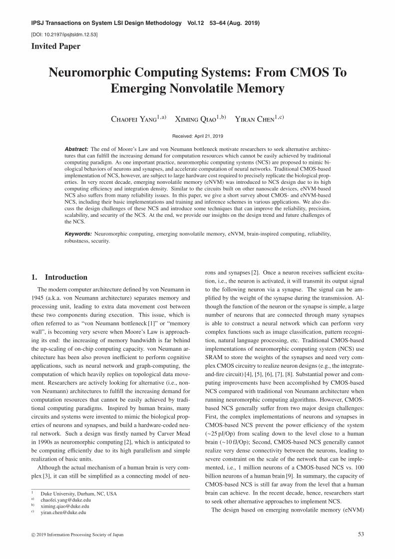
in his dissertation [23] using chalcogenide glass. By heating thedevice differently, PCM can switch between amorphous phase(high resistance state, or HRS) and crystalline phase (low re-sistance state, or LRS). There are two major research direc-tions of PCM device engineering: The traditional way focuses onsearching for viable material alternatives of Ge2S b2Te5 (GST);A later approach, which is called Interfacial Phase Change Mem-ory (IPCM) [24], leverages GeTe−S b2Te3 superlattice to achievenon-thermal phase changes by simply using laser pulse to changethe coordination state of the Germanium atoms. We can carefullycontrol the heating process of a PCM cell to obtain multiple inter-mediate phases and hence and realize multi-level cell (MLC) de-
Fig. 1 Cross section view of a PCM cell [27].
Fig. 2 MTJ structure [28]: (a) Antiparallel (HRS). (b) Parallel (LRS).(c) 1T1J STT-RAM cell structure.
sign that can store more than one bit on the cell. Figure 1 showsthe cross section view of a PCM cell. The PCM cell structuretypically consists of a thin layer of the chalcogenide sandwichedbetween two inert metal electrodes. Some researchers argue thatall two-terminal eNVM devices, including PCM, should be con-sidered as special types of memristors [25], [26].2.1.2 Spin-Transfer Torque Random-Access Memory (STT-
RAM)STT-RAM is a promising eNVM technology that features non-
volatility, fast read/write speed (< 10 ns), high programming en-durance (> 1015 cycles), zero standby power and good scalabil-ity [11]. STT-RAM utilizes the spin-transfer torque (STT) effectto switch the resistance of the magnetic tunnel junction (MTJ),which is the storage device of the STT-RAM cell. Figure 2 showsthe basic structure of MTJ and the popular one-transistor-one-MTJ (1T1J) STT-RAM cell structure. In the MTJ, a metal oxidebarrier layer (e.g., MgO) is sandwiched between two magneticlayers, namely, reference layer and free layer, respectively. Themagnetization of the reference layer is fixed while that of the freelayer can be switched by passing a spin-polarized current fromdifferent directions. When the magnetization directions of thereference layer and the free layer are in antiparallel (parallel), theMTJ shows as an HRS (LRS). Very recently, binary stochasticsynaptic behavior has been demonstrated based on the stochasticswitching nature of the MTJ devices at low voltages and program-ming time-scales [29].2.1.3 Resistive Random Access Memory (RRAM)
RRAM is one type of eNVMs that is built on dielectric solid-state materials and is often referred to as “memristors”. Based onthe formation and annihilation of a conducting region between
c© 2019 Information Processing Society of Japan 54
IPSJ Transactions on System LSI Design Methodology Vol.12 53–64 (Aug. 2019)
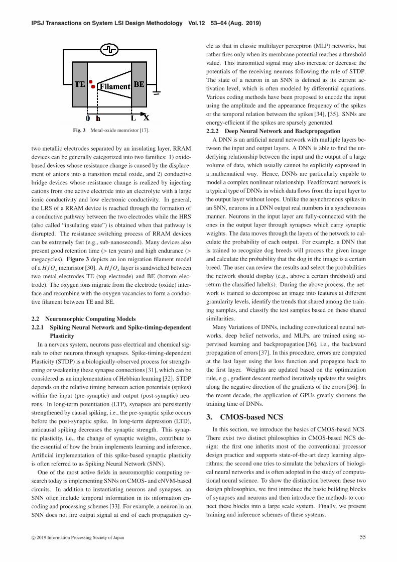
Fig. 3 Metal-oxide memristor [17].
two metallic electrodes separated by an insulating layer, RRAMdevices can be generally categorized into two families: 1) oxide-based devices whose resistance change is caused by the displace-ment of anions into a transition metal oxide, and 2) conductivebridge devices whose resistance change is realized by injectingcations from one active electrode into an electrolyte with a largeionic conductivity and low electronic conductivity. In general,the LRS of a RRAM device is reached through the formation ofa conductive pathway between the two electrodes while the HRS(also called “insulating state”) is obtained when that pathway isdisrupted. The resistance switching process of RRAM devicescan be extremely fast (e.g., sub-nanosecond). Many devices alsopresent good retention time (> ten years) and high endurance (>megacycles). Figure 3 depicts an ion migration filament modelof a H f Ox memristor [30]. A H f Ox layer is sandwiched betweentwo metal electrodes TE (top electrode) and BE (bottom elec-trode). The oxygen ions migrate from the electrode (oxide) inter-face and recombine with the oxygen vacancies to form a conduc-tive filament between TE and BE.
2.2 Neuromorphic Computing Models2.2.1 Spiking Neural Network and Spike-timing-dependent
PlasticityIn a nervous system, neurons pass electrical and chemical sig-
nals to other neurons through synapses. Spike-timing-dependentPlasticity (STDP) is a biologically-observed process for strength-ening or weakening these synapse connections [31], which can beconsidered as an implementation of Hebbian learning [32]. STDPdepends on the relative timing between action potentials (spikes)within the input (pre-synaptic) and output (post-synaptic) neu-rons. In long-term potentiation (LTP), synapses are persistentlystrengthened by causal spiking, i.e., the pre-synaptic spike occursbefore the post-synaptic spike. In long-term depression (LTD),anticausal spiking decreases the synaptic strength. This synap-tic plasticity, i.e., the change of synaptic weights, contribute tothe essential of how the brain implements learning and inference.Artificial implementation of this spike-based synaptic plasticityis often referred to as Spiking Neural Network (SNN).
One of the most active fields in neuromorphic computing re-search today is implementing SNNs on CMOS- and eNVM-basedcircuits. In addition to instantiating neurons and synapses, anSNN often include temporal information in its information en-coding and processing schemes [33]. For example, a neuron in anSNN does not fire output signal at end of each propagation cy-
cle as that in classic multilayer perceptron (MLP) networks, butrather fires only when its membrane potential reaches a thresholdvalue. This transmitted signal may also increase or decrease thepotentials of the receiving neurons following the rule of STDP.The state of a neuron in an SNN is defined as its current ac-tivation level, which is often modeled by differential equations.Various coding methods have been proposed to encode the inputusing the amplitude and the appearance frequency of the spikesor the temporal relation between the spikes [34], [35]. SNNs areenergy-efficient if the spikes are sparsely generated.2.2.2 Deep Neural Network and Backpropagation
A DNN is an artificial neural network with multiple layers be-tween the input and output layers. A DNN is able to find the un-derlying relationship between the input and the output of a largevolume of data, which usually cannot be explicitly expressed ina mathematical way. Hence, DNNs are particularly capable tomodel a complex nonlinear relationship. Feedforward network isa typical type of DNNs in which data flows from the input layer tothe output layer without loops. Unlike the asynchronous spikes inan SNN, neurons in a DNN output real numbers in a synchronousmanner. Neurons in the input layer are fully-connected with theones in the output layer through synapses which carry synapticweights. The data moves through the layers of the network to cal-culate the probability of each output. For example, a DNN thatis trained to recognize dog breeds will process the given imageand calculate the probability that the dog in the image is a certainbreed. The user can review the results and select the probabilitiesthe network should display (e.g., above a certain threshold) andreturn the classified label(s). During the above process, the net-work is trained to decompose an image into features at differentgranularity levels, identify the trends that shared among the train-ing samples, and classify the test samples based on these sharedsimilarities.
Many Variations of DNNs, including convolutional neural net-works, deep belief networks, and MLPs, are trained using su-pervised learning and backpropagation [36], i.e., the backwardpropagation of errors [37]. In this procedure, errors are computedat the last layer using the loss function and propagate back tothe first layer. Weights are updated based on the optimizationrule, e.g., gradient descent method iteratively updates the weightsalong the negative direction of the gradients of the errors [36]. Inthe recent decade, the application of GPUs greatly shortens thetraining time of DNNs.
3. CMOS-based NCS
In this section, we introduce the basics of CMOS-based NCS.There exist two distinct philosophies in CMOS-based NCS de-sign: the first one inherits most of the conventional processordesign practice and supports state-of-the-art deep learning algo-rithms; the second one tries to simulate the behaviors of biologi-cal neural networks and is often adopted in the study of computa-tional neural science. To show the distinction between these twodesign philosophies, we first introduce the basic building blocksof synapses and neurons and then introduce the methods to con-nect these blocks into a large scale system. Finally, we presenttraining and inference schemes of these systems.
c© 2019 Information Processing Society of Japan 55
IPSJ Transactions on System LSI Design Methodology Vol.12 53–64 (Aug. 2019)
3.1 Fundamental Components3.1.1 Synapse Structure
Von Neumann architecture and near-memory computing.Some DNN accelerators simulate neurons and synapses usingvon Neumann processors such as conventional CPU/GPUs. Themajor reason is that the large size of modern DNN models, i.e.,more than 108 weights of state-of-the-art image recognition mod-els [38], is far beyond the capacity of existing on-chip SRAM.Synaptic weights are stored in an off-chip DRAM and loaded tothe processor on demand. Although such a design suffers fromlow computing efficiency and long memory access latency, it isstill the most popular approach to simulate large scale DNNs dueto its good scalability and ease usage.
Recent research focus in this area is designing a better memoryhierarchy that can minimize the access overhead of the synapticweights. For example, Chen et al. [39] utilizes a hybrid on-chipmemory design composed of embedded DRAM and SRAM tostore the synaptic weights and a multiplier array to accelerate thecomputations, achieving an energy efficiency 150× higher thanGPUs. Low-level caches are directly controlled by the compilerto maximize their utilization [40]. These designs are often re-ferred to as “near-memory computing”. In some recent designs,the data processing logic is customized according to the compu-tation pattern of the targeted DNN workloads [41].
Processing-in-memory (PIM). Diffrent from von Neumannprocessors, the “processing-in-memory (PIM)” implementationallows synaptic weights to be stored, computed, and updated in-side the memory cells, without any significant data movement.The memory-centric design makes PIM a natural candidate forSNN acceleration. One benefit is that for SNN learning algo-rithms, the continuous accesses to all synaptic weights can beimplemented efficiently in PIM. The hardware architecture ofPIM is also close to the structure of a biological neural network.Using 6-transistor SRAM cells to store digital synapses, state-of-the-art implementation achieves a density of 2.1 million single-bitsynapses per mm2 at 14 nm technology node [8]. An alternativeapproach is to use floating-gate transistors for analog synapses.As a type of a nonvolatile memory, the weights stored in thefloating-gate transistors are updated by charging and discharg-ing the gates through current pulses. This process can be utilizedto directly simulate the learning rule of SNNs, which makes itespecially suitable for SNN acceleration [42], [43].
In CMOS-based DNN accelerator research, the recent focusshift to PIM is mainly triggered by energy efficiency. A SRAM-based DNN accelerator from Biswas et al. [44] achieves up to100× energy reduction comparing to the discrete memory andcomputing implementation. However, the scalability of this de-sign is greatly hindered by the low integration density of 6-transistor SRAM cells [45]. The typical on-chip memory size isa few MB, which only allows the execution of MNIST [46]-levelapplications even binary neural network is applied.3.1.2 Neurons
In computational neural science study, a variety of neuroncircuits were designed to simulate biological neuronal models.Those neuronal models can be as simple as integrate-and-firewhich contains only accumulation and threshold detection; or
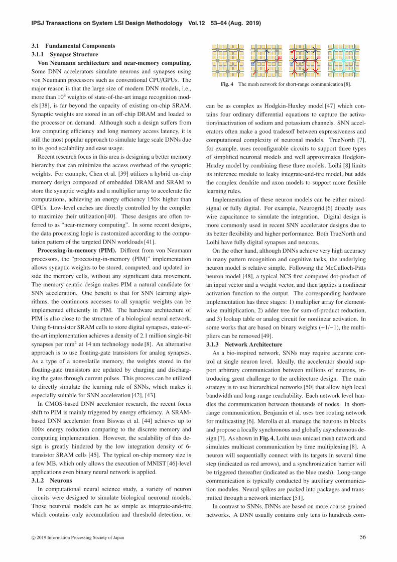
Fig. 4 The mesh network for short-range communication [8].
can be as complex as Hodgkin-Huxley model [47] which con-tains four ordinary differential equations to capture the activa-tion/inactivation of sodium and potassium channels. SNN accel-erators often make a good tradesoff between expressiveness andcomputational complexity of neuronal models. TrueNorth [7],for example, uses reconfigurable circuits to support three typesof simplified neuronal models and well approximates Hodgkin-Huxley model by combining these three models. Loihi [8] limitsits inference module to leaky integrate-and-fire model, but addsthe complex dendrite and axon models to support more flexiblelearning rules.
Implementation of these neuron models can be either mixed-signal or fully digital. For example, Neurogrid [6] directly useswire capacitance to simulate the integration. Digital design ismore commonly used in recent SNN accelerator designs due toits better flexibility and higher performance. Both TrueNorth andLoihi have fully digital synapses and neurons.
On the other hand, although DNNs achieve very high accuracyin many pattern recognition and cognitive tasks, the underlyingneuron model is relative simple. Following the McCulloch-Pittsneuron model [48], a typical NCS first computes dot-product ofan input vector and a weight vector, and then applies a nonlinearactivation function to the output. The corresponding hardwareimplementation has three stages: 1) multiplier array for element-wise multiplication, 2) adder tree for sum-of-product reduction,and 3) lookup table or analog circuit for nonlinear activation. Insome works that are based on binary weights (+1/−1), the multi-pliers can be removed [49].3.1.3 Network Architecture
As a bio-inspired network, SNNs may require accurate con-trol at single neuron level. Ideally, the accelerator should sup-port arbitrary communication between millions of neurons, in-troducing great challenge to the architecture design. The mainstrategy is to use hierarchical networks [50] that allow high localbandwidth and long-range reachability. Each network level han-dles the communication between thousands of nodes. In short-range communication, Benjamin et al. uses tree routing networkfor multicasting [6]. Merolla et al. manage the neurons in blocksand propose a locally synchronous and globally asynchronous de-sign [7]. As shown in Fig. 4, Loihi uses unicast mesh network andsimulates multicast communication by time multiplexing [8]. Aneuron will sequentially connect with its targets in several timestep (indicated as red arrows), and a synchronization barrier willbe triggered thereafter (indicated as the blue mesh). Long-rangecommunication is typically conducted by auxiliary communica-tion modules. Neural spikes are packed into packages and trans-mitted through a network interface [51].
In contrast to SNNs, DNNs are based on more coarse-grainednetworks. A DNN usually contains only tens to hundreds com-
c© 2019 Information Processing Society of Japan 56
IPSJ Transactions on System LSI Design Methodology Vol.12 53–64 (Aug. 2019)
putation nodes (or layers), each of which contains thousands tomillions of operations. DNN accelerators usually process onlyone or a few nodes at each time, regardless of the overall networktopology. Each node usually has a very regular computation pat-tern like matrix multiplication and convolution. As such, DNNaccelerators use a synchronous on-chip network to perform singlelayer execution. For example, Google TPU uses systolic array toaccelerate matrix multiplications [40] and Eyeriss uses a special-ized row-stationary architecture to accelerate convolutions [41].Multi-chip parallelization is based on data parallelism, i.e., allaccelerators execute the same model on different data. The majorcomponent of the communication between accelerators is modelsynchronization and is independent to DNN’s network topology.Zou et al. [52] proposed a tree network for accelerator intercon-nection.
3.2 Training and Inference Schemes3.2.1 SNNs
In SNNs, rate coding is often used to convert discrete spikesinto continuous values. The average rate of neuronal spikes rep-resents the output value, and the convergence of spiking rate takesmultiple cycles of computation. Although the inference operationof SNNs is not as straightforward as that of DNNs, the trainingof SNNs can be implemented more efficiently using more locallearning rules. Spike-timing-dependent Plasticity (STDP) is aclassical learning rule for SNNs, i.e.,
Δwi j =∑
k,k′F(tik − t jk′
), (1)
F(Δt) =
⎧⎪⎪⎨⎪⎪⎩A+ exp (−Δt/τ+) Δt > 0−A− exp (Δt/τ−) Δt < 0
(2)
As shown in Eq. (1), for neuron i and j, the synaptic weight wi j isupdated according to the timing difference between pre-synapticspikes tik and post-synaptic spikes t jk′ . Equation (2) gives an ex-ample update rule using exponential functions. Notice that eachweight update only relies on the information of its adjacent neu-rons. Such bio-inspired local learning rule introduces much lowerhardware overhead of the training circuits than that of the BP al-gorithm used in DNN training [53].
Although it is hardware friendly, the SNN trained by STDPnormally cannot achieve the same level of accuracy of the DNNtrained by BP [54]. There have been extensive works searchingfor better biologically feasible alternatives of BP. The segre-gated dendrites (SD) model [55] simulates neocortical pyramidalneuron that has two segregated compartments. Park et al. showthat a SD-based neuromorphic chip can achieve near-DNN ac-curacy while keeping a low training overhead, i.e., 7.5% energyconsumption overhead comparing to more than 50% overhead inprevious works [56].3.2.2 DNNs
Gradient descent is a popular way to train DNNs. ThroughBP, all synaptic weights are directly updated to minimized thefinal loss. For example, we assume a 3-layer DNN F(x) =fw1 ( fw2 ( fw3 (x))) where x as input and wi as the layers’ weights.Given a loss function L(F(x)), the gradients of wi are computedthrough the chain rule:
∂L∂w1=∂L∂ fw1
∂ fw1
∂w1, (3)
∂L∂w2=∂L∂ fw1
∂ fw1
∂ fw2
∂ fw2
∂w2, (4)
∂L∂w3=∂L∂ fw1
∂ fw1
∂ fw2
∂ fw2
∂ fw3
∂ fw3
∂w3. (5)
Although being effective as an optimization algorithm, BP is notbiological feasible and may introduces large hardware cost to sup-port the training process. The main problem of BP is that itscomputation is not local: calculating the gradient of one networklayer requires the activation and weight information of other lay-ers. Therefore, to support training, the hardware must providesome form of information passage that connects distant layers. Inthe accelerators based on von Neumann architecture, this passageis implemented using large off-chip memory. Intermediate results(i.e., ∂L/∂ fw1 and ∂ fw1/∂ fw2 ) are stored off-chip and accessed ondemand. The direct result of such a design is that GPUs can re-quire over 10 GB of memory to achieve enough training paral-lelism [57]. Preforming BP on PIM architecture is almost im-possible due to the controversy between the limited capacity ofSRAM array and the high precision required by the BP process.
4. eNVM-based NCS
In this section, we will discuss the design of eNVM-basedNCS, including the fundamental components such as neurons andsynapses, the training and inference schemes, and a detailed com-parison with CMOS-based NCS. We will show that eNVM-basedNCS demonstrate some great potentials in various aspects. Wealso discuss the challenges of eNVM-based NCS.
4.1 Fundamental Components4.1.1 Synapses
In an eNVM-based NCS, adjusting a synaptic weight is usuallyrealized by programming the eNVM device between LRS (SET)and HRS (RESET).
PCM as a synapse. Synaptic weight can be represented by theresistance of a PCM cell, which is programmed by heating thedevice in different ways. The SET process can be implementedincrementally by applying repetitive pulses to slowly crystallizethe PCM device. The RESET process, however, involves meltand quench and tends to be an abrupt process.
A two-PCM approach was proposed to implement STDP, i.e.,using separate devices for LTP and LTD, respectively [58]. Whena pre-synaptic neuron spikes, it sends out a read pulse and enters“LTP mode”. If the post-synaptic neuron spikes during this pe-riod, the LTP synapse receives a partial SET pulse. Otherwise, theLTD synapse is programmed. Symmetric and asymmetric STDPwere also implemented with a single PCM cell as a synapse [59],where staircase down pulses of varying amplitudes were used forpartial SET.
STT-RAM as a synapse. STT-RAM uses the current to RE-
SET (or SET) the polarization of the free ferromagnetic layer.During the RESET (SET) process, a positive (negative) voltagedifference is applied between the source line (SL) and the bit line(BL) in Fig. 2. The current amplitude required to reverse the di-
c© 2019 Information Processing Society of Japan 57
IPSJ Transactions on System LSI Design Methodology Vol.12 53–64 (Aug. 2019)
rection of the free ferromagnetic layer is determined by the sizeand aspect ratio of MTJ and the write pulse duration.
Vincent et al. used STT-RAM to implement a stochastic mem-ristive synapse by carefully choosing the current and durationtime of programming pulses to implement controlled switchingprobabilities [29]. At device level, binary MTJ is the most com-mon choice due to the mature fabrication process to control themagnetic anisotropy [60]. Multi-bit storage cells can also be re-alized by either producing more stable states [61] or the stack ofMTJs [62].
RRAM as a synapse. During the RESET process of a RRAMcell, a partially ruptured conductive filament region with a highresistance per unit length is formed aside the conductive filamentregion with a low resistance per unit length. The memristor thenswitches from LRS to HRS. During the SET process, the rupturedconductive filament region shrinks, thus switching the memristorfrom HRS to LRS. Note that the memristor resistance can beprogrammed to any arbitrary value by applying a programmingcurrent with different pulse widths or magnitudes. The memris-tor resistance changes only when the applied voltage is above athreshold.
Choi et al. reported a gradual RESET switching with increas-ing voltages in a GdOx-based RRAM with abrupt SET switch-ing [63]. Another approach is to combine the abrupt SET opera-tion and binary synaptic devices to implement a stochastic learn-ing rule [64]. Piccolboni et al. reported a H f O2-based verticalRRAM (VRRAM) technology [65], where each synapse is com-posed of a stack of RRAMs with one common transistor.4.1.2 Neurons
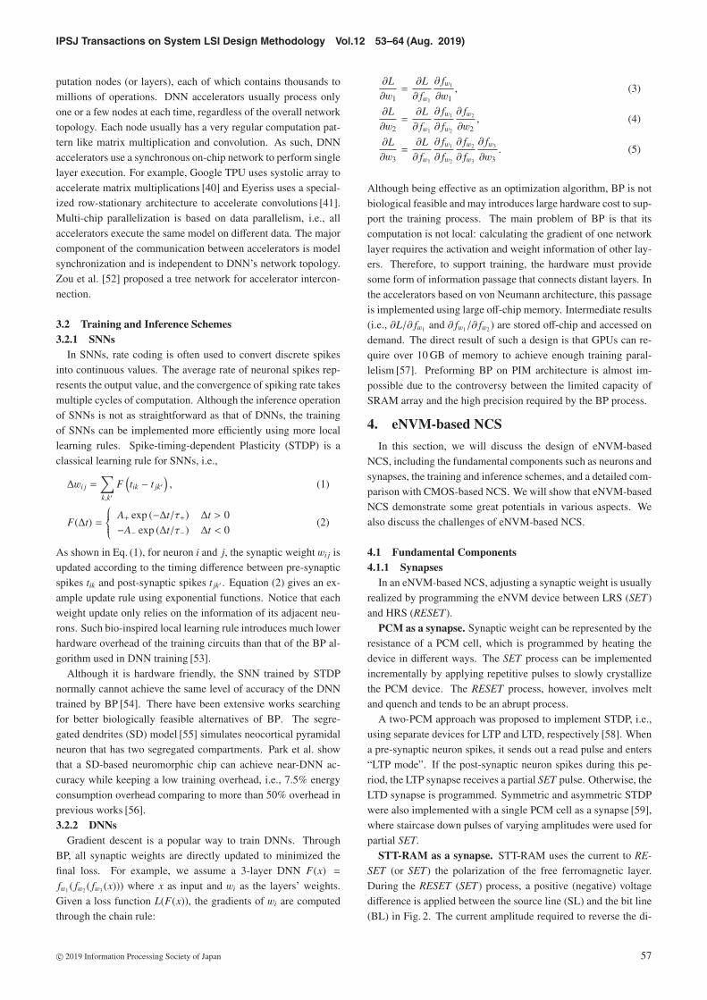
Emulation of neuronal dynamics, including the equilibrium po-tential, the transient dynamics, and the process of neurotrans-mission, is the key to realizing biologically plausible NCS [66].However, the complex neuronal dynamics must often be simpli-fied for efficient hardware realizations [67]. The integration ofthe post-synaptic potentials and the subsequent firing event arethe two most important dynamical components. Figure 5 (a) de-picts the schematic of an integrate-and-fire (IF) design featuringhigh speed and low power consumption [68]. During the opera-tion, the BL voltage Vy continues increasing until it reaches Vth.Then the differential pair (M1 − M4) together with the followingtwo cascaded inverters (M5 − M7 and M10 − M12) generates ahigh voltage at Vs, which in turn enables the discharging transis-tor M13. Consequently, Vy decreases quickly and eventually turnsoff M13. As such, the firing of one output spike at Vout is com-pleted and a new iteration of IF starts. Liu et al. implemented andsimulated the IF design with IBM 130 nm technology [68]. Thewaveforms of Vy, Vs, and Vout under the fastest firing frequencyare shown in Fig. 5 (b).4.1.3 Crossbar Structure
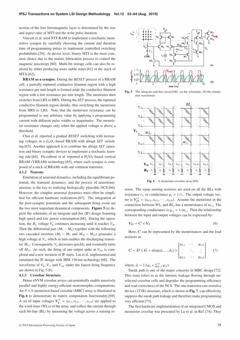
Dense eNVM crossbar arrays can potentially enable massivelyparallel and highly energy-efficient neuromorphic computations.An N ×N memristor-based crossbar (MBC) array is illustrated inFig. 6 to demonstrate its matrix computation functionality [69].A set of input voltages V T
I = {vI,1, vI,2, · · · , vI,N} are applied tothe word-lines (WLs) of the array, and collect the current througheach bit-line (BL) by measuring the voltage across a sensing re-
Fig. 5 The integrate-and-fire circuit [68]: (a) the schematic, (b) the simula-tion waveforms.
Fig. 6 A memristor crossbar array [69].
sistor. The same sensing resistors are used on all the BLs withresistance rs, or conductance gs = 1/rs. The output voltage vec-tor is V T
O = {vO,1, vO,2, · · · , vO,N}. Assume the memristor in theconnection between WLi and BLj has a memristance of mi, j. Thecorresponding conductance is gi, j = 1/mi, j. Then the relationshipbetween the input and output voltages can be expressed by:
VO = C × VI (6)
Here, C can be represented by the memristances and the loadresistors as:
C =D ×G = diag(d1, ..., dN) ×
⎡⎢⎢⎢⎢⎢⎢⎢⎢⎢⎢⎢⎢⎣
g1,1 · · · g1,N
.... . .
...
gN,1 · · · gN,N
⎤⎥⎥⎥⎥⎥⎥⎥⎥⎥⎥⎥⎥⎦(7)
where, di = 1/(gs +∑N
k=1 gi,k).Sneak path is one of the major concerns in MBC design [72].
This issue refers to as the intrinsic leakage flowing through un-selected crossbar cells and degrades the programming efficiencyand read correctness of the NCS. The one-transistor-one-resistivedevice (1T1R) structure, which is shown in Fig. 7, can effectivelysuppress the sneak path leakage and therefore make programmingvery efficient [73].
The first hardware implementation of an integrated CMOS andmemristor crossbar was presented by Lu et al. in Ref. [74]. They
c© 2019 Information Processing Society of Japan 58
IPSJ Transactions on System LSI Design Methodology Vol.12 53–64 (Aug. 2019)
Table 1 A detailed comparison of human brain, GPU, CMOS- and eNVM-based NCS.
System Type Neuron Synapse # neurons # synapses Power Energy/Connection Technology Trainability
Human Brain [9] Biology Diverse Diverse 100 B 1015 20 W 10 fJ 10 μm BiologyGPU [70] Digital - - - - 180 W 7 nJ 16 nm Any
Neurogrid [6] AnalogAdaptive
Quadratic IFShared
Dendrite65 k 100 M 150 mW 100 pJ 180 nm No
True North [7] DigitalAdaptive
Exponential IF4-bit Digital 1 M 256 M 72 mW 25 pJ 28 nm No
Loihi [8] Digital Leaky IF Non-fixed 131 k 126 M 73 mW 23.6 pJ 14 nm STDP
PCM [71] Analog Leaky IFAnalogWeight
256 64 k - 0.9 pJ 90 nm STDP
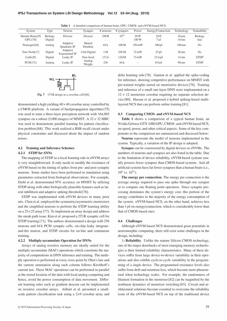
Fig. 7 1T1R design in a crossbar cell [68].
demonstrated a high yielding 40×40 crossbar array controlled bya CMOS platform. A variant of backpropagation algorithm [75]was used to train a three-layer perceptron network with 164,885synapses on a subset (5,000 images) of MNIST. A 32 × 32 MBCwas used to demonstrate parallel learning for pattern classifica-tion problem [68]. This work realized a BSB recall circuit underphysical constraints and discussed about the impact of randomnoises.
4.2 Training and Inference Schemes4.2.1 STDP for SNNs
The mapping of STDP as a local learning rule in eNVM arraysis very straightforward. It only needs to modify the resistance ofeNVM based on the timing of spikes from pre- and post-synapticneurons. Some studies have been performed in simulation usingparameters extracted from biological observations. For example,Diehl et al. demonstrated 95% accuracy on MNIST by utilizingSTDP along with other biologically plausible features such as lat-eral inhibition and adaptive spiking threshold [76].
STDP was implemented with eNVM devices in many priorarts. Chen et al. employed the symmetric/asymmetric memristorsand the simplified neurons to perform the STDP learning abilityon a 25×25 array [77]. To implement an array design and addressthe sneak-path issue, Kim et al. proposed a 2T1R synaptic cell forSTDP learning [71]. The authors demonstrated a design with 256neurons and 64 k PCM synaptic cells, on-chip leaky integrate-and-fire neuron, and STDP circuits for on-line and continuoustraining.4.2.2 Multiply-accumulate Operation for DNNs
Arrays of analog resistive memory are ideally suited for themultiply-accumulate (MAC) operations which constitute the ma-jority of computations in DNN inference and training. The multi-ply operation is performed at every cross-point by Ohm’s law andthe current summation along each column follows Kirchhoff’scurrent law. These MAC operations can be performed in parallelat the stored location of the data with local analog computing andhence, avoid the power consumption of data movement. Differ-ent learning rules such as gradient descent can be implementedon resistive crossbar arrays. Alibart et al. presented a small-scale pattern classification task using a 2×9 crossbar array and
delta learning rule [78]. Gamrat et al. applied the spike-codingfor inference, showing competitive performance on MNIST withpre-trained weights stored on memristive devices [79]. Trainingand inference of a small one-layer DNN were implemented on a12 × 12 memristor crossbar requiring no separate selection de-vice [80]. Hassan et al. proposed a hybrid spiking-based multi-layered NCS that can perform online training [81].
4.3 Comparing CMOS- and eNVM-based NCSTable 1 shows a comparison of a typical human brain, an
Nvidia Geforce GTX 1080 GPU, CMOS- and eNVM-based NCS,on speed, power, and other critical aspects. Some of the key com-ponents in the comparison are summarized and discussed below:
Neuron represents the model of neurons implemented in thesystem. Typically, a variation of the IF design is adopted.
Synapse can be constructed by digital devices or eNVMs. Thenumbers of neurons and synapses are also listed in the table. Dueto the limitation of device reliability, eNVM-based systems usu-ally possess fewer synapses than CMOS-based systems. And allartificial systems have far fewer synapses than a human brain (i.e.,106 vs. 1015).
The energy per connection. The energy per connection is theaverage energy required to pass one spike through one synapseor to compute one floating point operation. Since synaptic pro-cessing dominates the system’s energy cost, this portion of theenergy contributes to the majority of the energy consumption ofthe system. eNVM-based NCS, on the other hand, achieves lessthan 1 pJ on energy/connection, which is considerably lower thanthat of CMOS-based ones.
4.4 ChallengesAlthough eNVM-based NCS demonstrated great potentials in
neuromorphic computing, there still exist some challenges in thedesign, including:
1) Reliability. Unlike the mature Silicon CMOS technology,one of the major drawbacks of most emerging memory technolo-gies is their limited reliability characteristics. Many of these de-vices suffer from large device-to-device variability in their oper-ations and also exhibit cycle-to-cycle variability in the program-ming of a single device. The programmed resistance levels alsosuffer from drift and retention loss, which become more phenom-enal when technology scales. For example, the randomness offilament formation in the memrisor [82] can be magnified by thenonlinear dynamics of memrisor switching [83]. Circuit and ar-chitectural solutions become essential to overcome the reliabilityissue of the eNVM-based NCS on top of the traditional device
c© 2019 Information Processing Society of Japan 59
IPSJ Transactions on System LSI Design Methodology Vol.12 53–64 (Aug. 2019)
engineering solutions.2) Integration. The integration of MBC and CMOS-based
neuron circuits also generate many unique design challenges. Forexample, the interconnect IR-drop in memristor arrays severelylimits the scale of MBCs and hence hinders the design scalability.Liu et al. showed that both reading (recall) and writing (training)of the MBC will encounter severe reliability issues when the arraysize is beyond 64 × 64 [18]. In addition, the fabrication processof memristor devices is still under development, thus still achiev-ing unsatisfying yield at the array level. Stuck-on and stuck-offdefects are often observed [84]. Also, due to the intrinsic mecha-nism of the memristor, analog memristance values are vulnerableto read disturbance, that is, the memristance could drift from itsoriginally programmed value after a number of accesses. There-fore, an real-time feedback controller might be needed to traceand control such drift.
3) Security. Neuromorphic computing are widely used inmany applications for advanced data processing, and often im-plements proprietary algorithms. While DNNs have achieved re-markable success in advanced intelligent applications, security-related issues gradually become severe. For example, the learn-ing model running on an embedded device is exposed to the riskof being attacked by malicious users who have physical access tothe device [20]. Attackers can also send hand-crafted data intothe system and achieve anticipated purposes, e.g., to fool themodel’s predictions in testing phase using adversarial attack [85]or to compromise the model in training phase using poisoningattack [86].
5. EDA-based Solutions
In this section, we will discuss some EDA-based solutions toaddress the design challenges of eNVM-based NCS, includingreliability, precision, scalability, and security.
5.1 Reliability and IntegrationProgramming a memristor to a specific state can be very chal-
lenging because real-time monitoring the memristor state is notpractical [87]. Liu et al. proposed a noise-eliminating trainingmethod over a new crossbar structure to minimize the noise accu-mulation during the MBC training and improve the trained systemperformance, i.e., the pattern recall rate [17]. The sensitivity ofthe MBC programming to the process variations and input signalnoise was quantitatively analyzed. A digital-assisted initializationstep for MBC training was also introduced to reduce the trainingfailure rate as well as the training time. Experiment results wereevaluated on multiple 512 × 512 MBC computing engines. Xiaet al. proposed a fault-tolerant online training method that alter-nates between two phases [88]. The fault-detection phase used aquiescent-voltage comparison method to obtain faulty cells dur-ing training. The fault-tolerant phase used a threshold-trainingmethod and a re-mapping scheme to tolerate the faults.
Another issue of MBCs is that the voltage applied to the twoterminals of a memristor is affected by the device location in thecrossbar and the resistance states of all other memristors. Liu etal. proposed a novel system reduction scheme that significantlylowers the required dimension of the memristor crossbars in NCS
while maintaining high computing accuracy [18]. An IR-dropcompensation technique was also proposed to overcome the ad-verse impacts of the wire resistance and the sneak-path problemin large memristor crossbar designs [18]. Another approach is topartition a large network into many small ones in lower dimen-sion [89].
The training of NCS can be further improved if the realistichardware limits are taken into consideration. Liu et al. presenteda quantitative analysis on the impact of device imperfections andcircuit design constraints and proposed a novel variation-awaretraining scheme to enhance the training robustness of MBC-basedNCS by actively compensating the impact of device variationsand optimizing the mapping scheme from computations to cross-bars [19]. Most eNVM devices show nonlinear and asymmetricswitching behaviors. These characteristics may prevent backpro-pogation algorithm from locating optimal weights during train-ing [90]. Such nonlinear behaviors also degrade the system toler-ance to noises. Gong et al. established a practical methodologybased on Gaussian process regression to address this issue [91].The proposed methodology is independent on switching mecha-nisms and applicable to various eNVM devices.
5.2 PrecisionThe performance of eNVM-based NCS usually depends on
how accurately the state of the devices can be programmed.Alibart et al. designed a simple write algorithm to tune deviceconductance at a specific bias point within its dynamic range evenin the presence of large variations in switching behavior [92]. Ex-cept for device engineering optimization, algorithm-level tech-nique is also helpful to relax the requirement of the resistancestate resolution. By modifying the regularization in training, theweight distribution can be tuned to fit the resistance values [93].In this way, algorithm-level weights are tailored to enhance theaccuracy of eNVM-based NCS.
To better alleviate the impact of device variations, binarizedneural networks (BNNs) can be implemented in eNVM-basedNCS. BNNs only allow binary synapses of +1 and −1. Compareto floating point DNNs, BNNs avoids the complex matrix mul-tiplications by leveraging simple binary operations [94]. Phamet al. proposed a Memristor-CMOS hybrid circuits of BNNs,where single-column and double-column memristor BNNs werepresented and activation function are realized using CMOS cir-cuits [95]. Experiment results showed that the memristor BNNscould recognize as many as 90% MNIST digits when the mem-ristance variation is as large as 25%. Additionally, Nandakumaret al. proposed a mixed-precision architecture that combines acomputational memory unit storing the synaptic weights with adigital processing unit and an additional memory unit that storedthe accumulated weight updates in high precision [96].
5.3 ScalabilityTo further increase the design density of NCS, various works
are proposed to implement 3D structured eNVMs. Researchersfrom Intel demonstrated the ability to stack multiple layers ofPCM arrays within a single die [97]. To alleviate the write over-head of STT-RAM in a 3D multi-core environment, Mishra et
c© 2019 Information Processing Society of Japan 60
IPSJ Transactions on System LSI Design Methodology Vol.12 53–64 (Aug. 2019)
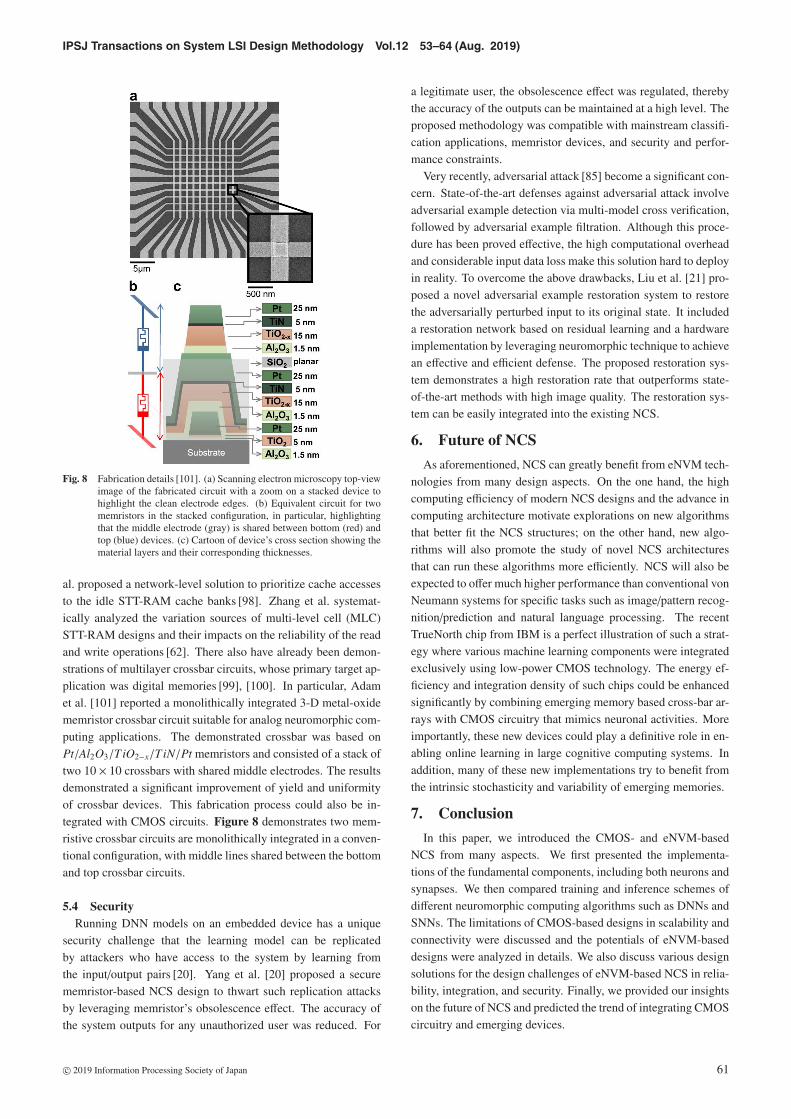
Fig. 8 Fabrication details [101]. (a) Scanning electron microscopy top-viewimage of the fabricated circuit with a zoom on a stacked device tohighlight the clean electrode edges. (b) Equivalent circuit for twomemristors in the stacked configuration, in particular, highlightingthat the middle electrode (gray) is shared between bottom (red) andtop (blue) devices. (c) Cartoon of device’s cross section showing thematerial layers and their corresponding thicknesses.
al. proposed a network-level solution to prioritize cache accessesto the idle STT-RAM cache banks [98]. Zhang et al. systemat-ically analyzed the variation sources of multi-level cell (MLC)STT-RAM designs and their impacts on the reliability of the readand write operations [62]. There also have already been demon-strations of multilayer crossbar circuits, whose primary target ap-plication was digital memories [99], [100]. In particular, Adamet al. [101] reported a monolithically integrated 3-D metal-oxidememristor crossbar circuit suitable for analog neuromorphic com-puting applications. The demonstrated crossbar was based onPt/Al2O3/TiO2−x/TiN/Pt memristors and consisted of a stack oftwo 10 × 10 crossbars with shared middle electrodes. The resultsdemonstrated a significant improvement of yield and uniformityof crossbar devices. This fabrication process could also be in-tegrated with CMOS circuits. Figure 8 demonstrates two mem-ristive crossbar circuits are monolithically integrated in a conven-tional configuration, with middle lines shared between the bottomand top crossbar circuits.
5.4 SecurityRunning DNN models on an embedded device has a unique
security challenge that the learning model can be replicatedby attackers who have access to the system by learning fromthe input/output pairs [20]. Yang et al. [20] proposed a securememristor-based NCS design to thwart such replication attacksby leveraging memristor’s obsolescence effect. The accuracy ofthe system outputs for any unauthorized user was reduced. For
a legitimate user, the obsolescence effect was regulated, therebythe accuracy of the outputs can be maintained at a high level. Theproposed methodology was compatible with mainstream classifi-cation applications, memristor devices, and security and perfor-mance constraints.
Very recently, adversarial attack [85] become a significant con-cern. State-of-the-art defenses against adversarial attack involveadversarial example detection via multi-model cross verification,followed by adversarial example filtration. Although this proce-dure has been proved effective, the high computational overheadand considerable input data loss make this solution hard to deployin reality. To overcome the above drawbacks, Liu et al. [21] pro-posed a novel adversarial example restoration system to restorethe adversarially perturbed input to its original state. It includeda restoration network based on residual learning and a hardwareimplementation by leveraging neuromorphic technique to achievean effective and efficient defense. The proposed restoration sys-tem demonstrates a high restoration rate that outperforms state-of-the-art methods with high image quality. The restoration sys-tem can be easily integrated into the existing NCS.
6. Future of NCS
As aforementioned, NCS can greatly benefit from eNVM tech-nologies from many design aspects. On the one hand, the highcomputing efficiency of modern NCS designs and the advance incomputing architecture motivate explorations on new algorithmsthat better fit the NCS structures; on the other hand, new algo-rithms will also promote the study of novel NCS architecturesthat can run these algorithms more efficiently. NCS will also beexpected to offer much higher performance than conventional vonNeumann systems for specific tasks such as image/pattern recog-nition/prediction and natural language processing. The recentTrueNorth chip from IBM is a perfect illustration of such a strat-egy where various machine learning components were integratedexclusively using low-power CMOS technology. The energy ef-ficiency and integration density of such chips could be enhancedsignificantly by combining emerging memory based cross-bar ar-rays with CMOS circuitry that mimics neuronal activities. Moreimportantly, these new devices could play a definitive role in en-abling online learning in large cognitive computing systems. Inaddition, many of these new implementations try to benefit fromthe intrinsic stochasticity and variability of emerging memories.
7. Conclusion
In this paper, we introduced the CMOS- and eNVM-basedNCS from many aspects. We first presented the implementa-tions of the fundamental components, including both neurons andsynapses. We then compared training and inference schemes ofdifferent neuromorphic computing algorithms such as DNNs andSNNs. The limitations of CMOS-based designs in scalability andconnectivity were discussed and the potentials of eNVM-baseddesigns were analyzed in details. We also discuss various designsolutions for the design challenges of eNVM-based NCS in relia-bility, integration, and security. Finally, we provided our insightson the future of NCS and predicted the trend of integrating CMOScircuitry and emerging devices.
c© 2019 Information Processing Society of Japan 61
IPSJ Transactions on System LSI Design Methodology Vol.12 53–64 (Aug. 2019)
Acknowledgments This work was supported by NSF-1725456, NSF-1822085, and the memberships of NSF IUCRCfor ASIC from Horizon Robotics, Unisound, etc.
References
[1] Backus, J.: Can programming be liberated from the von Neumannstyle? A functional style and its algebra of programs, ACM (2007).
[2] Mead, C.: Neuromorphic electronic systems, Proc. IEEE, Vol.78,No.10, pp.1629–1636 (1990).
[3] Sterling, P. and Laughlin, S.: Principles of neural design, MIT Press(2015).
[4] Farquhar, E., Gordon, C. and Hasler, P.: A field programmable neu-ral array, IEEE International Symposium on Circuits and Systems(ISCAS), pp.4114–4117 (2006).
[5] Poon, C.-S. and Zhou, K.: Neuromorphic silicon neurons and large-scale neural networks: Challenges and opportunities, Frontiers inNeuroscience, Vol.5, p.108 (2011).
[6] Benjamin, B.V., Gao, P., McQuinn, E., Choudhary, S.,Chandrasekaran, A.R., Bussat, J.-M., Alvarez-Icaza, R., Arthur, J.V.,Merolla, P.A. and Boahen, K.: Neurogrid: A mixed-analog-digitalmultichip system for large-scale neural simulations, Proc. IEEE,Vol.102, No.5, pp.699–716 (2014).
[7] Merolla, P.A., Arthur, J.V., Alvarez-Icaza, R., Cassidy, A.S., Sawada,J., Akopyan, F., Jackson, B.L., Imam, N., Guo, C., Nakamura, Y.,et al.: A million spiking-neuron integrated circuit with a scalablecommunication network and interface, Science, Vol.345, No.6197,pp.668–673 (2014).
[8] Davies, M., Srinivasa, N., Lin, T.-H., Chinya, G., Cao, Y., Choday,S.H., Dimou, G., Joshi, P., Imam, N., Jain, S., et al.: Loihi: A neu-romorphic manycore processor with on-chip learning, IEEE Micro,Vol.38, No.1, pp.82–99 (2018).
[9] Furber, S.: Large-scale neuromorphic computing systems, Journal ofNeural Engineering, Vol.13, No.5, p.051001 (2016).
[10] Wong, H.-S.P., Raoux, S., Kim, S., Liang, J., Reifenberg, J.P.,Rajendran, B., Asheghi, M. and Goodson, K.E.: Phase change mem-ory, Proc. IEEE, Vol.98, No.12, pp.2201–2227 (2010).
[11] Hosomi, M., Yamagishi, H., Yamamoto, T., Bessho, K., Higo, Y.,Yamane, K., Yamada, H., Shoji, M., Hachino, H., Fukumoto, C., etal.: A novel nonvolatile memory with spin torque transfer magneti-zation switching: Spin-RAM, IEEE International Electron DevicesMeeting (IEDM), pp.459–462 (2005).
[12] Wong, H.-S.P., Lee, H.-Y., Yu, S., Chen, Y.-S., Wu, Y., Chen, P.-S.,Lee, B., Chen, F.T. and Tsai, M.-J.: Metal–oxide RRAM, Proc.IEEE, Vol.100, No.6, pp.1951–1970 (2012).
[13] Burr, G.W., Shelby, R.M., Sebastian, A., Kim, S., Kim, S., Sidler,S., Virwani, K., Ishii, M., Narayanan, P., Fumarola, A., et al.:Neuromorphic computing using non-volatile memory, Advances inPhysics: X, Vol.2, No.1, pp.89–124 (2017).
[14] Liu, X., Mao, M., Liu, B., Li, H., Chen, Y., Li, B., Wang,Y., Jiang, H., Barnell, M., Wu, Q., et al.: RENO: A high-efficient reconfigurable neuromorphic computing accelerator design,ACM/EDAC/IEEE Design Automation Conference (DAC), pp.1–6(2015).
[15] Song, L., Qian, X., Li, H. and Chen, Y.: Pipelayer: A pipelinedreram-based accelerator for deep learning, IEEE International Sym-posium on High Performance Computer Architecture (HPCA),pp.541–552 (2017).
[16] Chen, F., Song, L. and Chen, Y.: ReGAN: A pipelined ReRAM-based accelerator for generative adversarial networks, Asia andSouth Pacific Design Automation Conference (ASP-DAC), pp.178–183 (2018).
[17] Liu, B., Hu, M., Li, H., Mao, Z.-H., Chen, Y., Huang, T.and Zhang, W.: Digital-assisted noise-eliminating training formemristor crossbar-based analog neuromorphic computing engine,ACM/EDAC/IEEE Design Automation Conference (DAC), pp.1–6(2013).
[18] Liu, B., Li, H., Chen, Y., Li, X., Huang, T., Wu, Q. and Barnell, M.:Reduction and IR-drop compensations techniques for reliable neu-romorphic computing systems, IEEE/ACM International Conferenceon Computer-Aided Design (ICCAD), pp.63–70 (2014).
[19] Liu, B., Li, H., Chen, Y., Li, X., Wu, Q. and Huang, T.: Vortex:Variation-aware training for memristor x-bar, ACM/EDAC/IEEE De-sign Automation Conference (DAC), pp.1–6 (2015).
[20] Yang, C., Liu, B., Li, H., Chen, Y., Barnell, M., Wu, Q.,Wen, W. and Rajendran, J.: Security of neuromorphic comput-ing: Thwarting learning attacks using memristor’s obsolescence ef-fect, IEEE/ACM International Conference on Computer-Aided De-sign (ICCAD), pp.1–6 (2016).
[21] Liu, Y., Xie, Y. and Srivastava, A.: Neural trojans, IEEE Interna-
tional Conference on Computer Design (ICCD), pp.45–48 (2017).[22] Liu, B., Yang, C., Li, H., Chen, Y., Wu, Q. and Barnell, M.: Security
of neuromorphic systems: Challenges and solutions, IEEE Interna-tional Symposium on Circuits and Systems (ISCAS), pp.1326–1329(2016).
[23] Sie, C.: Memory devices using bistable resistivity in amorphous As-Te-Ge films, PhD Thesis, Ph.D. dissertation, Iowa State University,Ames, IA (1969).
[24] Simpson, R., Fons, P., Kolobov, A., Fukaya, T., Krbal, M., Yagi,T. and Tominaga, J.: Interfacial phase-change memory, Nature Nan-otechnology, Vol.6, No.8, p.501 (2011).
[25] Chua, L.: Resistance switching memories are memristors, AppliedPhysics A, Vol.102, No.4, pp.765–783 (2011).
[26] Mellor, C.: HP and Hynix to produce the memristor goods by 2013,The Register (2012).
[27] Rajendran, B., Karidis, J., Lee, M., Breitwisch, M., Burr, G., Shih,Y., Cheek, R., Schrott, A., Lung, H. and Lam, C.: Analytical modelfor reset operation of phase change memory, IEEE InternationalElectron Devices Meeting (IEDM), pp.1–4 (2008).
[28] Zhang, Y., Wang, X., Li, H. and Chen, Y.: STT-RAM cell optimiza-tion considering MTJ and CMOS variations, IEEE Trans. Magnetics,Vol.47, No.10, pp.2962–2965 (2011).
[29] Vincent, A.F., Larroque, J., Locatelli, N., Romdhane, N.B., Bichler,O., Gamrat, C., Zhao, W.S., Klein, J.-O., Galdin-Retailleau, S. andQuerlioz, D.: Spin-transfer torque magnetic memory as a stochas-tic memristive synapse for neuromorphic systems, IEEE Trans.Biomedical Circuits and Systems (TBioCAS), Vol.9, No.2, pp.166–174 (2015).
[30] Yu, S., Wu, Y. and Wong, H.-S.P.: Investigating the switching dy-namics and multilevel capability of bipolar metal oxide resistiveswitching memory, Applied Physics Letters, Vol.98, No.10, p.103514(2011).
[31] Taylor, M.: The problem of stimulus structure in the behavioural the-ory of perception, S. Afr. J. Psychol, Vol.3, pp.23–45 (1973).
[32] Hebb, D.O.: The organization of behavior; a neuropsycholocigaltheory, John Wiley & Sons Inc. (1949).
[33] Maass, W.: Networks of spiking neurons: The third generation ofneural network models, Neural Networks, Vol.10, No.9, pp.1659–1671 (1997).
[34] Zambrano, D., Nusselder, R., Scholte, H.S. and Bohte, S.: Efficientcomputation in adaptive artificial spiking neural networks, arXivpreprint arXiv:1710.04838 (2017).
[35] Rueckauer, B. and Liu, S.-C.: Conversion of analog to spiking neuralnetworks using sparse temporal coding, IEEE International Sympo-sium on Circuits and Systems (ISCAS), pp.1–5 (2018).
[36] Goodfellow, I., Bengio, Y. and Courville, A.: Deep learning, MITpress (2016).
[37] Rumelhart, D.E., Hinton, G.E. and Williams, R.J.: Learning repre-sentations by back-propagating errors, Nature, Vol.323, No.9 (1986).
[38] Cheng, Y., Wang, D., Zhou, P. and Zhang, T.: A survey ofmodel compression and acceleration for deep neural networks, arXivpreprint arXiv:1710.09282 (2017).
[39] Chen, Y., Luo, T., Liu, S., Zhang, S., He, L., Wang, J., Li, L.,Chen, T., Xu, Z., Sun, N., et al.: Dadiannao: A machine-learningsupercomputer, IEEE/ACM International Symposium on Microarchi-tecture (MICRO), pp.609–622 (2014).
[40] Jouppi, N.P., Young, C., Patil, N., Patterson, D., Agrawal, G., Bajwa,R., Bates, S., Bhatia, S., Boden, N., Borchers, A., et al.: In-datacenterperformance analysis of a tensor processing unit, IEEE/ACM Interna-tional Symposium on Computer Architecture (ISCA), pp.1–12 (2017).
[41] Chen, Y.-H., Krishna, T., Emer, J.S. and Sze, V.: Eyeriss: An energy-efficient reconfigurable accelerator for deep convolutional neural net-works, IEEE Journal of Solid-State Circuits (JSSC), Vol.52, No.1,pp.127–138 (2017).
[42] Yang, H., Sheu, B.J. and Lee, J.-C.: A nonvolatile analog neuralmemory using floating-gate MOS transistors, Analog Integrated Cir-cuits and Signal Processing, Vol.2, No.1, pp.19–25 (1992).
[43] Hindo, T.: Weight updating floating-gate synapse, Electronics Let-ters, Vol.50, No.17, pp.1190–1191 (2014).
[44] Biswas, A. and Chandrakasan, A.P.: Conv-RAM: An energy-efficient SRAM with embedded convolution computation for low-power CNN-based machine learning applications, IEEE Interna-tional Solid-State Circuits Conference (ISSCC), pp.488–490 (2018).
[45] Zhang, J., Wang, Z. and Verma, N.: A machine-learning classifier im-plemented in a standard 6T SRAM array, IEEE Symposium on VLSICircuits (VLSI-Circuits), pp.1–2 (2016).
[46] LeCun, Y., Bottou, L., Bengio, Y., Haffner, P., et al.: Gradient-based learning applied to document recognition, Proc. IEEE, Vol.86,No.11, pp.2278–2324 (1998).
[47] Hodgkin, A.L. and Huxley, A.F.: A quantitative description of mem-brane current and its application to conduction and excitation in
c© 2019 Information Processing Society of Japan 62
IPSJ Transactions on System LSI Design Methodology Vol.12 53–64 (Aug. 2019)
nerve, The Journal of Physiology, Vol.117, No.4, pp.500–544 (1952).[48] McCulloch, W.S. and Pitts, W.: A logical calculus of the ideas im-
manent in nervous activity, Bulletin of Mathematical Biology, Vol.52,No.1-2, pp.99–115 (1990).
[49] Andri, R., Cavigelli, L., Rossi, D. and Benini, L.: YodaNN: An ar-chitecture for ultralow power binary-weight CNN acceleration, IEEETransactions on Computer-Aided Design of Integrated Circuits andSystems (TCAD), Vol.37, No.1, pp.48–60 (2018).
[50] Furber, S.B., Lester, D.R., Plana, L.A., Garside, J.D., Painkras, E.,Temple, S. and Brown, A.D.: Overview of the spinnaker system ar-chitecture, IEEE Trans. Computers, Vol.62, No.12, pp.2454–2467(2013).
[51] Wu, J., Furber, S. and Garside, J.: A programmable adaptive routerfor a GALS parallel system, 2009 15th IEEE Symposium on Asyn-chronous Circuits and Systems, pp.23–31 (2009).
[52] Zou, Y., Jin, X., Li, Y., Guo, Z., Wang, E. and Xiao, B.: Mariana:Tencent deep learning platform and its applications, Proc. VLDB En-dowment, Vol.7, No.13, pp.1772–1777 (2014).
[53] Schemmel, J., Briiderle, D., Griibl, A., Hock, M., Meier, K. andMillner, S.: A wafer-scale neuromorphic hardware system for large-scale neural modeling, IEEE International Symposium on Circuitsand Systems (ISCAS), pp.1947–1950 (2010).
[54] Kheradpisheh, S.R., Ganjtabesh, M., Thorpe, S.J. and Masquelier,T.: STDP-based spiking deep convolutional neural networks for ob-ject recognition, Neural Networks, Vol.99, pp.56–67 (2018).
[55] Guerguiev, J., Lillicrap, T.P. and Richards, B.A.: Towards deep learn-ing with segregated dendrites, eLife, Vol.6, p.e22901 (2017).
[56] Park, J., Lee, J. and Jeon, D.: 7.6 A 65nm 236.5 nJ/ClassificationNeuromorphic Processor with 7.5% Energy Overhead On-ChipLearning Using Direct Spike-Only Feedback, IEEE InternationalSolid-State Circuits Conference (ISSCC), pp.140–142 (2019).
[57] Meng, C., Sun, M., Yang, J., Qiu, M. and Gu, Y.: Training deepermodels by GPU memory optimization on TensorFlow, ML SystemsWorkshop in NIPS (2017).
[58] Suri, M., Bichler, O., Querlioz, D., Cueto, O., Perniola, L., Sousa,V., Vuillaume, D., Gamrat, C. and DeSalvo, B.: Phase change mem-ory as synapse for ultra-dense neuromorphic systems: Applicationto complex visual pattern extraction, International Electron DevicesMeeting (IEDM), pp.4.4.1–4.4.4 (2011).
[59] Kuzum, D., Jeyasingh, R.G. and Wong, H.-S.P.: Energy efficient pro-gramming of nanoelectronic synaptic devices for large-scale imple-mentation of associative and temporal sequence learning, Interna-tional Electron Devices Meeting (IEDM), pp.30.3.1–30.3.4 (2011).
[60] Yan, B., Chen, F., Zhang, Y., Song, C., Li, H. and Chen, Y.: Explor-ing the opportunity of implementing neuromorphic computing sys-tems with spintronic devices, Design, Automation & Test in EuropeConference & Exhibition (DATE), pp.109–112 (2018).
[61] Stainer, Q., Lombard, L., Mackay, K., Lee, D., Bandiera, S.,Portemont, C., Creuzet, C., Sousa, R. and Dieny, B.: Self-referencedmulti-bit thermally assisted magnetic random access memories, Ap-plied Physics Letters, Vol.105, No.3, p.032405 (2014).
[62] Zhang, Y., Zhang, L., Wen, W., Sun, G. and Chen, Y.: Multi-levelcell STT-RAM: Is it realistic or just a dream?, IEEE/ACM Interna-tional Conference on Computer-Aided Design (ICCAD), pp.526–532(2012).
[63] Choi, H., Jung, H., Lee, J., Yoon, J., Park, J., Seong, D.-J., Lee,W., Hasan, M., Jung, G.-Y. and Hwang, H.: An electrically modifi-able synapse array of resistive switching memory, Nanotechnology,Vol.20, No.34, p.345201 (2009).
[64] Yu, S., Gao, B., Fang, Z., Yu, H., Kang, J. and Wong, H.-S.P.:Stochastic learning in oxide binary synaptic device for neuromorphiccomputing, Frontiers in Neuroscience, Vol.7, p.186 (2013).
[65] Piccolboni, G., Molas, G., Portal, J., Coquand, R., Bocquet, M.,Garbin, D., Vianello, E., Carabasse, C., Delaye, V., Pellissier, C.,et al.: Investigation of the potentialities of Vertical Resistive RAM(VRRAM) for neuromorphic applications, IEEE International Elec-tron Devices Meeting (IEDM), pp.17.2.1–17.2.4 (2015).
[66] Gerstner, W., Kistler, W.M., Naud, R. and Paninski, L.: Neuronal dy-namics: From single neurons to networks and models of cognition,Cambridge University Press (2014).
[67] Indiveri, G., Linares-Barranco, B., Hamilton, T.J., Van Schaik, A.,Etienne-Cummings, R., Delbruck, T., Liu, S.-C., Dudek, P., Hafliger,P., Renaud, S., et al.: Neuromorphic silicon neuron circuits, Frontiersin Neuroscience, Vol.5, p.73 (2011).
[68] Liu, C., Yan, B., Yang, C., Song, L., Li, Z., Liu, B., Chen, Y., Li, H.,Wu, Q. and Jiang, H.: A spiking neuromorphic design with resistivecrossbar, ACM/EDAC/IEEE Design Automation Conference (DAC),pp.1–6 (2015).
[69] Hu, M., Li, H., Wu, Q., Rose, G.S. and Chen, Y.: Memristor cross-bar based hardware realization of BSB recall function, InternationalJoint Conference on Neural Networks (IJCNN), pp.1–7 (2012).
[70] Nvidia Geforce GTX 1080. available from 〈https://www.nvidia.com/en-us/geforce/products/10series/geforce-gtx-1080/〉, (accessed2019-03-14).
[71] Kim, S., Ishii, M., Lewis, S., Perri, T., BrightSky, M., Kim, W.,Jordan, R., Burr, G., Sosa, N., Ray, A., et al.: NVM neuromorphiccore with 64k-cell (256-by-256) phase change memory synaptic ar-ray with on-chip neuron circuits for continuous in-situ learning, IEEEInternational Electron Devices Meeting (IEDM), pp.17.1.1–17.1.4(2015).
[72] Flocke, A. and Noll, T.G.: Fundamental analysis of resistive nano-crossbars for the use in hybrid Nano/CMOS-memory, EuropeanSolid-State Circuits Conference (ESSCIRC), pp.328–331 (2007).
[73] Huang, J.-J., Tseng, Y.-M., Luo, W.-C., Hsu, C.-W. and Hou, T.-H.:One selector-one resistor (1S1R) crossbar array for high-density flex-ible memory applications, International Electron Devices Meeting(IEDM), pp.31.7.1–31.7.4 (2011).
[74] Kim, K.-H., Gaba, S., Wheeler, D., Cruz-Albrecht, J.M., Hussain, T.,Srinivasa, N. and Lu, W.: A functional hybrid memristor crossbar-array/CMOS system for data storage and neuromorphic applications,Nano Letters, Vol.12, No.1, pp.389–395 (2011).
[75] Burr, G.W., Shelby, R.M., Sidler, S., di Nolfo, C., Jang, J., Boybat, I.,Shenoy, R.S., Narayanan, P., Virwani, K., Giacometti, E.U., Kurdi,B.N. and Hwang, H.: Experimental Demonstration and Tolerancingof a Large-Scale Neural Network (165 000 Synapses) Using Phase-Change Memory as the Synaptic Weight Element, IEEE Trans. Elec-tron Devices (T-ED), Vol.62, No.11, pp.3498–3507 (2015).
[76] Diehl, P.U. and Cook, M.: Unsupervised learning of digit recognitionusing spike-timing-dependent plasticity, Frontiers in ComputationalNeuroscience, Vol.9, p.99 (2015).
[77] Chen, L., Li, C., Huang, T., He, X., Li, H. and Chen, Y.: STDP learn-ing rule based on memristor with STDP property, International JointConference on Neural Networks (IJCNN), pp.1–6 (2014).
[78] Alibart, F., Zamanidoost, E. and Strukov, D.B.: Pattern classifica-tion by memristive crossbar circuits using ex situ and in situ training,Nature Communications, Vol.4, p.2072 (2013).
[79] Gamrat, C., Bichler, O. and Roclin, D.: Memristive based devicearrays combined with spike based coding can enable efficient imple-mentations of embedded neuromorphic circuits, IEEE InternationalElectron Devices Meeting (IEDM), pp.4.5.1–4.5.7 (2015).
[80] Burr, G., Narayanan, P., Shelby, R., Sidler, S., Boybat, I., di Nolfo,C. and Leblebici, Y.: Large-scale neural networks implemented withnon-volatile memory as the synaptic weight element: Comparativeperformance analysis (accuracy, speed, and power), IEEE Interna-tional Electron Devices Meeting (IEDM), pp.4.4.1–4.4.4 (2015).
[81] Hassan, A.M., Yang, C., Liu, C., Li, H.H. and Chen, Y.: Hy-brid spiking-based multi-layered self-learning neuromorphic systembased on memristor crossbar arrays, Design, Automation & Test inEurope Conference & Exhibition (DATE), pp.776–781 (2017).
[82] Liu, Q., Long, S., Lv, H., Wang, W., Niu, J., Huo, Z., Chen,J. and Liu, M.: Controllable growth of nanoscale conductive fila-ments in solid-electrolyte-based ReRAM by using a metal nanocrys-tal covered bottom electrode, ACS Nano, Vol.4, No.10, pp.6162–6168 (2010).
[83] Chua, L.O.: Local activity is the origin of complexity, InternationalJournal of Bifurcation and Chaos (IJBC), Vol.15, No.11, pp.3435–3456 (2005).
[84] Liu, C., Hu, M., Strachan, J.P. and Li, H.: Rescuing memristor-basedneuromorphic design with high defects, ACM/EDAC/IEEE DesignAutomation Conference (DAC), pp.1–6 (2017).
[85] Goodfellow, I.J., Shlens, J. and Szegedy, C.: Explaining and har-nessing adversarial examples, International Conference on LearningRepresentations (ICLR) (2015).
[86] Yang, C., Wu, Q., Li, H. and Chen, Y.: Generative poisoning attackmethod against neural networks, arXiv preprint arXiv:1703.01340(2017).
[87] Jo, S.H., Chang, T., Ebong, I., Bhadviya, B.B., Mazumder, P. andLu, W.: Nanoscale memristor device as synapse in neuromorphicsystems, Nano Letters, Vol.10, No.4, pp.1297–1301 (2010).
[88] Xia, L., Liu, M., Ning, X., Chakrabarty, K. and Wang, Y.: Fault-tolerant training with on-line fault detection for rram-based neuralcomputing systems, ACM/EDAC/IEEE Design Automation Confer-ence (DAC), pp.1–6 (2017).
[89] Wang, Y., Wen, W., Liu, B., Chiarulli, D. and Li, H.: Group scissor:Scaling neuromorphic computing design to large neural networks,ACM/EDAC/IEEE Design Automation Conference (DAC), pp.1–6(2017).
[90] Shelby, R.M., Burr, G.W., Boybat, I. and Di Nolfo, C.: Non-volatilememory as hardware synapse in neuromorphic computing: A firstlook at reliability issues, IEEE International Reliability Physics Sym-posium (IRPS), pp.6A.1.1–6A.1.6, IEEE (2015).
[91] Gong, N., Ide, T., Kim, S., Boybat, I., Sebastian, A., Narayanan, V.
c© 2019 Information Processing Society of Japan 63
IPSJ Transactions on System LSI Design Methodology Vol.12 53–64 (Aug. 2019)
and Ando, T.: Signal and noise extraction from analog memory ele-ments for neuromorphic computing, Nature Communications, Vol.9,No.1, p.2102 (2018).
[92] Alibart, F., Gao, L., Hoskins, B.D. and Strukov, D.B.: High precisiontuning of state for memristive devices by adaptable variation-tolerantalgorithm, Nanotechnology, Vol.23, No.7, p.075201 (2012).
[93] Song, C., Liu, B., Wen, W., Li, H. and Chen, Y.: A quantization-aware regularized learning method in multilevel memristor-basedneuromorphic computing system, IEEE Non-Volatile Memory Sys-tems and Applications Symposium (NVMSA), pp.1–6 (2017).
[94] Courbariaux, M., Hubara, I., Soudry, D., El-Yaniv, R. and Bengio,Y.: Binarized neural networks: Training deep neural networks withweights and activations constrained to +1 or −1, arXiv preprintarXiv:1602.02830 (2016).
[95] Van Pham, K., Van Nguyen, T., Tran, S.B., Nam, H., Lee, M.J., Choi,B.J., Truong, S.N. and Min, K.-S.: Memristor Binarized Neural Net-works, Journal of Semiconductor Technology and Science (JSTS),Vol.18, No.5, pp.568–577 (2018).
[96] Nandakumar, S., Le Gallo, M., Boybat, I., Rajendran, B., Sebastian,A. and Eleftheriou, E.: Mixed-precision architecture based on com-putational memory for training deep neural networks, IEEE Interna-tional Symposium on Circuits and Systems (ISCAS), pp.1–5 (2018).
[97] McGrath, D.: Intel, Numonyx claim phase-change memory mile-stone, EE Times (2009).
[98] Mishra, A.K., Dong, X., Sun, G., Xie, Y., Vijaykrishnan, N. and Das,C.R.: Architecting on-chip interconnects for stacked 3D STT-RAMcaches in CMPs, ACM SIGARCH Computer Architecture News,Vol.39, No.3, pp.69–80 (2011).
[99] Kawahara, A., Azuma, R., Ikeda, Y., Kawai, K., Katoh, Y.,Hayakawa, Y., Tsuji, K., Yoneda, S., Himeno, A., Shimakawa, K.,et al.: An 8 Mb multi-layered cross-point ReRAM macro with 443MB/s write throughput, IEEE Journal of Solid-State Circuits (JSSC),Vol.48, No.1, pp.178–185 (2013).
[100] Liu, T., Yan, T.H., Scheuerlein, R., Chen, Y., Lee, J.K., Balakrishnan,G., Yee, G., Zhang, H., Yap, A., Ouyang, J., Sasaki, T., Addepalli,S., Al-Shamma, A., Chen, C., Gupta, M., Hilton, G., Joshi, S.,Kathuria, A., Lai, V., Masiwal, D., Matsumoto, M., Nigam, A.,Pai, A., Pakhale, J., Siau, C.H., Wu, X., Yin, R., Peng, L., Kang,J.Y., Huynh, S., Wang, H., Nagel, N., Tanaka, Y., Higashitani, M.,Minvielle, T., Gorla, C., Tsukamoto, T., Yamaguchi, T., Okajima, M.,Okamura, T., Takase, S., Hara, T., Inoue, H., Fasoli, L., Mofidi, M.,Shrivastava, R. and Quader, K.: A 130.7mm2 2-layer 32Gb ReRAMmemory device in 24nm technology, IEEE International Solid-StateCircuits Conference Digest of Technical Papers (ISSCC), pp.210–211 (2013).
[101] Adam, G.C., Hoskins, B.D., Prezioso, M., Merrikh-Bayat, F.,Chakrabarti, B. and Strukov, D.B.: 3-D memristor crossbars for ana-log and neuromorphic computing applications, IEEE Trans. ElectronDevices (T-ED), Vol.64, No.1, pp.312–318 (2017).
Chaofei Yang received B.S. fromTsinghua University and M.S. from Uni-versity of Pittsburgh in 2017. He is aPh.D. student in the Electrical and Com-puter Engineering department at DukeUniversity. His research interests includeDeep Learning Security and Neuromor-phic Computing.
Ximing Qiao obtained his B.S. in com-puter science at Peking University,Beijing, China, and is currently a Ph.D.student in computer engineering at DukeUniversity. His research interest lies atthe junction of machine learning andcomputer architecture, focusing on fastand efficient machine learning algorithm
and hardware.
Yiran Chen received B.S. and M.S. fromTsinghua University and Ph.D. fromPurdue University in 2005. After fiveyears in industry, he joined University ofPittsburgh in 2010 as Assistant Professorand then promoted to Associate Profes-sor with tenure in 2014, held Bicenten-nial Alumni Faculty Fellow. He now is
the Professor of the Department of Electrical and Computer En-gineering at Duke University and serving as the director of NSFIndustry-University Cooperative Research Center (IUCRC) forAlternative Sustainable and Intelligent Computing (ASIC) andco-director of Duke Center for Evolutionary Intelligence (CEI),focusing on the research of new memory and storage systems,machine learning and neuromorphic computing, and mobile com-puting systems. Dr. Chen has published one book and more than350 technical publications and has been granted 93 US patents.He serves or served the associate editor of several IEEE and ACMtransactions/journals and served on the technical and organiza-tion committees of more than 50 international conferences. Hereceived 6 best paper awards and 13 best paper nominations frominternational conferences. He is the recipient of NSF CAREERaward and ACM SIGDA outstanding new faculty award. He isthe Fellow of IEEE and Distinguished Member of ACM, a distin-guished lecturer of IEEE CEDA, and the recipient of the Hum-boldt Research Fellowship for Experienced Researchers.
(Invited by Editor-in-Chief: Nozomu Togawa)
c© 2019 Information Processing Society of Japan 64