Embed Size (px)
Citation preview

Neural networks : analog VLSI implementation andlearning algorithmsWithagen, H.C.A.M.
DOI:10.6100/IR494433
Published: 01/01/1997
Document VersionPublisher’s PDF, also known as Version of Record (includes final page, issue and volume numbers)
Please check the document version of this publication:
• A submitted manuscript is the author's version of the article upon submission and before peer-review. There can be important differencesbetween the submitted version and the official published version of record. People interested in the research are advised to contact theauthor for the final version of the publication, or visit the DOI to the publisher's website.• The final author version and the galley proof are versions of the publication after peer review.• The final published version features the final layout of the paper including the volume, issue and page numbers.
Link to publication
Citation for published version (APA):Withagen, H. C. A. M. (1997). Neural networks : analog VLSI implementation and learning algorithmsEindhoven: Technische Universiteit Eindhoven DOI: 10.6100/IR494433
General rightsCopyright and moral rights for the publications made accessible in the public portal are retained by the authors and/or other copyright ownersand it is a condition of accessing publications that users recognise and abide by the legal requirements associated with these rights.
• Users may download and print one copy of any publication from the public portal for the purpose of private study or research. • You may not further distribute the material or use it for any profit-making activity or commercial gain • You may freely distribute the URL identifying the publication in the public portal ?
Take down policyIf you believe that this document breaches copyright please contact us providing details, and we will remove access to the work immediatelyand investigate your claim.
Download date: 26. Jun. 2018


Neural Networks:
Analog VLSI Implementation
and Lear11ing Algorithms

Cover design by Jan van Boesschoten
Printed by: Haveka b.v., Alblasserdam, The Netherlands

Neural Networks:
Analog VLSI Implementation
and Learning Algorithms
PROEFSCHRIFT
ter verkrijging van de graad van doctor aan de Technische U niversiteit Eindhoven, op gezag van
de Rector Magnificus, prof. dr. M. Rem, voor een commissie aangewezen door het College
van Dekanen in het openbaar te verdedigen op dinsdag 17 juni 1997 om 16.00 uur
door
Hendrik Carolus Arthur Maria Withagen
geboren te Bergen op Zoom

Dit proefschrift is goedgekeurd door de promotoren:
prof. dr. ir. W.M.G. van Bokhoven en prof. dr . ir . R.H.J.M. Otten
Copromotor: dr. ir. J.A. Hegt
@Copyright 1997 H.C.A.M. Withagen All rights reserved . No part of this publication may be reproduced, stored in a retrieval system , or transmitted, in any form or by any means, electronic, mechanical, photocopying, recording, or otherwise, without the prior written permission from the copyright owner.
CIP-DATA LIBRARY TECHNISCHE UNIVERSITEIT EINDHOVEN
Withagen, Hendrik C.A.M.
Neural networks: analog VLSI implementation and learning algorithms I by Hendrik C.A.M. Withagen. -Eindhoven: Technische Universiteit Eindhoven, 1997. Proefschrift. - ISBN 90-386-0350-9 NUGI 852 Trefw.: analoge geintegreerde schakelingen I neurale netwerken I lerende machines I kunstmatige intelligentie ; algoritmen. Subject headings: analogue processing circuits I neural chips I learning (artificial intelligence).

Summary
Neural networks are capable of solving complex tasks (e.g. speech and handwriting recognition) based on the presentation of a large number of examples. During learning, parameters in the network are adjusted according to a learning rule.
In this thesis, a number of aspects related to the electronic realization of neural networks will be discussed. In analogy with the human brain , an analog implementation of neural networks will be pursued using simple, small, possibly non-ideal building blocks; neurons and synapses.
In order to be able to build large networks, neurons and synapses are implemented on separate chips. Several chips can be combined to realize arbitrary feed-forward network topologies. Flexibility in network topology introduces the need for scaling of quantities in a network. An optimal scaling will be determined through a statistical analysis of the influence of errors in a network. In most cases, these errors are caused by quantization of synapse weight values.
Two implementation approaches will be considered. A time-sampled, pulse stream implementation where analog values are encoded using binary signals and an analog time-continuous implementation. In the latter case, a complete test system consisting of 2 synapse and 2 neuron chips organized in a 2-layer feed-forward network has been realized . The propagation delay per layer is in the order of lJ.Ls independent of the number of synapses and neurons per layer. A general comparison between the two approaches shows that both computation schemes have comparable performance for low power consumption values. Furthermore, general high-level models for both synapses and neurons will be introduced.
Several learning algorithms to be used in conjunction with the realized
1

2
chips will be considered. From a point of view of flexibility, a global, digital implementation of a learning algorithm has preference. This approach can best be combined with digital storage of synapse weight values and a periodic refresh to the analog feed-forward neural network implementation.

Samenvatting
Neurale netwerken zijn in staat oplossingen te bieden voor complexe problemen (bijv. spraak- en handschrift-herkenning) op basis van grate aantallen aangeboden correcte voorbeelden. Tijdens het leerproces worden parameters in het netwerk bijgesteld volgens een leerregel.
In dit proefschrift worden verschillende aspecten beschreven die betrekking hebben op de elektronische implementatie van neurale netwerken. Analoog aan de menselijke hersenen is gekozen voor een analoge elektronische implementatie waarbij gebruik wordt gemaakt van eenvoudige, kleine en mogelijk niet-ideale elementen; neuronen en synapsen.
Grote netwerken worden gerealiseerd door chips te combineren waarop neuronen en synapsen apart zijn ge"implementeerd. Iedere gewenste feedforward netwerk architectuur kan op deze manier worden gerealiseerd. Deze ftexibiliteit in architectuur introduceert de noodzaak van schaling van grootheden in een netwerk. Een optimale vorm van schaling wordt bepaald aan de hand van een statistische analyse van de invloed van fouten in een netwerk. Deze fouten worden meestal veroorzaakt door kwantisatie van gewichtswaarden in synapsen.
Twee implementatie methoden zullen worden bekeken. Een tijd-discrete, puis methode waarbij analoge waarden worden gerepresenteerd door middel van repeterende binaire signalen en een analoge, tijd-continue methode. Een vergelijking tussen de twee methoden toont aan dat beide vergelijkbare prestaties leveren. In het geval van de analoge, tijd-continue implementatie is een compleet systeem gerealiseerd. Dit systeem bestaat uit 2 synapse en 2 neuron chips die gezamenlijk een 2-laags feed-forward netwerk realiseren. Onafhankelijk van het aantal synapsen of neuronen in een laag, is de vertraging per laag in het gerealiseerde netwerk ongeveer lfLS. Van de gerealiseerde synapsen en neuronen zijn algemene modellen opgesteld die gebruikt kunnen
3

4
worden tijdens simulaties van te realiseren netwerken.
Een aantal leer-algoritmen die in combinatie met de gerealiseerde chips kunnen worden gebruikt, zijn bestudeerd. Uit het oogpunt van flexibiliteit kan het best gekozen worden voor een globale, digitale implementatie van een leerregel. Gecombineerd met de digitale opslag van gewichtswaarden en periodieke verversing naar het analoge feed-forward netwerk, Ievert dit het beste resultaat.

Contents
1 Introduction 1.1 Definitions .
1.1.1 Neuron .. 1.1.2 Networks
1.2 Learning . . ... 1.2.1 Gradient Descent 1.2.2 Learning Rate . . 1.2.3 Global or Local Minima 1.2.4 Back-Propagation .. 1.2.5 Weight Perturbation 1.2.6 Stochastic Learning . 1.2.7 Update Strategies . .
2 Systems 2.1 Flexibility ...... . 2.2 Scaling ... ... .. .
2.2 .1 Network Model 2.2.2 Solution . ...
2.2.3 Hardware Implementation Considerations 2.2.4 Conclusion
2.3 Signals . . . . . . . . 2.4 Chip Floor-plan ...
2.4.1 Synapse Chip 2.4.2 Neuron Chip
2.5 Weight Storage ... 2.5.1 Digital Storage 2.5.2 Non-volatile Storage 2.5.3 Capacitive Storage
5
9 10 10 12
13 15 15 16 17 18 19 22
25
25 27 28 31 33 34
34 35 36 38 39 39 40 41

6 CONTENTS
3 Implementation 43
4
5
3.1 Pulse Stream Approach . . . . . . . . . . . . . . . . 43 3.1.1 Overview of Pulse Stream Modulations . . . 44 3.1.2 Coherent Pulse Width Modulation (CPWM) 46 3.1.3 Pulse Stream Arithmetic . . . . . . . . . . . 48 3.1.4 Performance Analysis of CPWM Systems. . 50 3.1.5 Performance Comparison of CPWM and Analog Mul-
ti pliers . . . . . . 55 3.1.6 Building Blocks . . . 59
3.2 Analog Implementation . . . 70 3.2.1 Existing realizations 71 3.2.2 Synapse . . . . . 72 3.2.3 Neuron . . . . . . 80 3.2.4 Complete System 85
3.3 Modeling . . . . . . . . 87 3.3.1 Synapse Model 88 3.3.2 Neuron Model . 90
Learning 93 93 94 95 95 97 98 99
4.1 Back-Propagation . 4.1.1 Implementation . . 4.1.2 Offset in forward path 4.1.3 Offset in backward path 4.1.4 Offset cancellation 4.1.5 Conclusion
4.2 Semi-parallel perturbation 4.3 Fully parallel perturbation 4.4 Alopex . .. 4.5 Probabilistic Optimization 4.6 Learning Experiments
4.6.1 Epochs. 4.6.2 Parity-4 4.6.3 Parity-5 .. 4.6.4 Function Approximation 4.6.5 Conclusion
4.7 Weight Leakage . 4.8 Conclusion . . .
Concluding Remarks
101 102 104 105 106 107 108 108 110 111 112
115

CONTENTS 7
Bibliography 119
A System Details 131
B ANANAS 135
c Learning Experiments Details 139
D Circuit Details 143
Acknowledgements 145
Curriculum Vitae 147

8 CONTENTS

Chapter 1
Introduction
Although the current generation of computers provides large computational power in the field of problems which can be described algorithmically, cog
nitive tasks are still hard to solve. Examples of such tasks are face, speech, and handwriting recognition. Besides the fact that describing such problems and the way to solve them are very difficult, if not impossible, solving the task for a number of known situations is not sufficient. A certain level of generalization should be achieved to be able to provide adequate responses to inputs which have never been seen by a system.
The human brain is an unsurpassed system capable of learning a task based on the presentation of examples. It consists of a large number of small and simple computational units (neurons) which have a high degree of interconnectivity (synapses). The whole system has a relatively low degree of activity. Neurons communicate using pulse-shaped signals with frequencies in the order of 100 Hz. The learning mechanism used by the human brain is currently unknown as is the way information is stored. Cognitive tasks seem to be natural to the human brain while algorithmical problems are much harder.
In an effort to mimic the capabilities of the human brain, a lot of research has been put into distributed parallel systems and the way such systems can be trained to perform certain tasks. In recent years, completely parallel hardware implementations have been emerging. Two main approaches can be distinguished: 1) a digital approach in which units and communication between units are realized with an (almost) unlimited accuracy at a medium fast rate using digital signals and elements and, 2) an analog approach where a less accurate implementation is used (in analogy with the human brain) at a high speed.
9

10 CHAPTER 1. INTRODUCTION
Here, analog implementations of neural networks will be pursued using simple, small, possibly non-ideal (with respect to the mathematical way neural networks are described) building blocks. In contrast with most implementations reported in the literature, where a lot of effort is put into realizing 'perfect' building blocks1 , here a learning algorithm should be able to deal with non-idealities. As such, the whole of network and learning algorithm forms the complete system. The learning algorithm itself could also be implemented in hardware (analog or digital), thereby realizing a complete stand alone system capable of learning complex, non-algorithmic, cognitivelike tasks based on presentation of examples.
In the remainder of the current chapter, neural networks in general are described, introducing the used notation and several well-known learning algorithms. For a more detailed description of neural networks the reader is referred to the literature, e.g. [HKP91].
In chapter 2, issues which become apparent when neural networks are implemented in hardware will be discussed, as well as the general outlines for a flexible analog multi-chip implementation.
Two analog implementation approaches will be presented in chapter 3: a time-sampled, pulse stream approach where analog values are encoded using binary signals and an analog, time-continuous implementation. In the latter case, a complete test system has been rea lized. In the case of chapter 3, it is assumed that the reader has a basic knowledge of analog VLSI [IF94, AH87].
Chapter 4 reports on the use and implementation of learning algorithms in conjunction with a complete analog neural network implementation. In a complete setup consisting of several analog chips and a host computer, several learning experiments are performed .
1.1 Definitions
In this section, basic concepts and definitions for all terms used in describing neural networks and learning algorithms are provided.
1.1.1 Neuron
A neuron has one or more inputs x 1 ,x2 ,x3 , •. • .. ,XN and one output y. An input to a neuron is either an input of the network the neuron is part of, the output of another neuron , or its own output. The inputs are usually
1 For example, a linear multiplicative relationship in a synapse (in an overall non-linear system).

1.1. DEFINITIONS 11
weighted, i.e. an input Xi is multiplied by a weight Wi· The weighted inputs 81 , 8 2, 83 , ..... , 8N are added to form a sum 8. In most cases, a threshold () is also added to the weighted sum. This sum forms the argument of a non-linear function f. The output of the non-linear function is the output of the neuron. Figure 1.1 shows a block diagram of a neuron. Equation 1.1
y
Figure 1.1: A neuron
describes the operation of the neuron.
Y = j(8) = f (~ WiXi + ()( -1)) {1.1)
In most cases, the threshold contribution is treated as an extra input x 0 to the neuron. By choosing xo = -1 and wo = (), equation 1.1 simplifies to:
{1.2)
The extra input is also called the bias input of the neuron. The non-linear function f usually is a sigmoid-shaped, bounded, mono
tonic rising function which saturates for both large negative and positive values. Several functions fall in this category. Two frequently used choices are:
1 !(8) = 1 + e-f3s
j(8) = tanh(/38)
{1.3)
{1.4)
where f3 controls the steepness. For the extreme case of f3 -+ oo both 1.3 and 1.4 result in a binary threshold unit first proposed by [MP43).
12 CHAPTER 1. INTRODUCTION
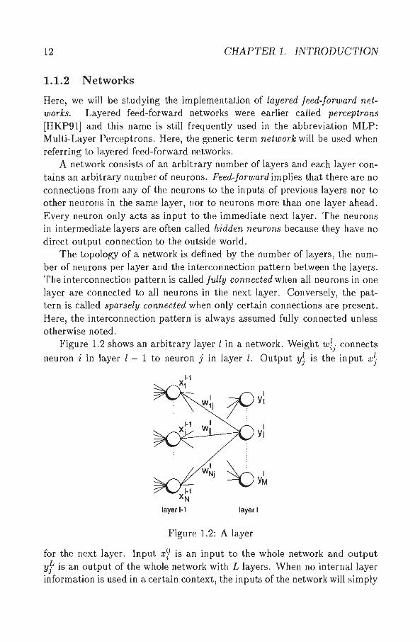
1.1.2 Networks
Here, we will be studying the implementation of layered feed-forward networks. Layered feed-forward networks were earlier called perceptrons [HKP91] and this name is still frequently used in the abbreviation MLP: Multi-Layer Perceptrons. Here, the generic term network will be used when referring to layered feed-forward networks.
A network consists of an arbitrary number of layers and each layer contains an arbitrary number of neurons. Feed-forward implies that there are no connections from any of the neurons to the inputs of previous layers nor to other neurons in the same layer, nor to neurons more than one layer ahead. Every neuron only acts as input to the immediate next layer. The neurons in intermediate layers are often called hidden neurons because they have no direct output connection to the outside world.
The topology of a network is defined by the number of layers, the number of neurons per layer and the interconnection pattern between the layers. The interconnection pattern is called fully connected when all neurons in one layer are connected to all neurons in the next layer. Conversely, the pattern is called sparsely connected when only certain connections are present. Here, the interconnection pattern is always assumed fully connected unless otherwise noted.
Figure 1.2 shows an arbitrary layer l in a network. Weight wL connects
neuron i in layer l- 1 to neuron j in layer l . Output y~ is the input x~
layer 1-1 layer I
Figure 1.2: A layer
for the next layer. Input x? is an input to the whole network and output yf is an output of the whole network with L layers. When no internal layer information is used in a certain context, the inputs of the network will simply

1.2. LEARNING 13
be denoted by Xi and similarly the outputs of the network are denoted by Yj. The inputs and outputs are usually grouped into vectors~ and ;y_ respectively. The inputs to a network are not counted as a layer. Consequently a network with one hidden layer is called a two-layer network. Note that an L-layer network has L layers of connections and L - 1 hidden layers. Figure 1.3 shows a two-layer network with 3 inputs, 4 neurons in the hidden layer, and 1 output. Bias inputs of the neurons are usually not drawn. The standard notation for a network with this topology is: a 3-4-1 network.
Figure 1.3: A 3-4-1 network
1.2 Learning
The functionality of a neural network is determined by the combination of the topology and the values of the weights in the network . The topology is usually chosen fixed 2 and the weights are determined by a learning algorithm.
The objective of a learning algorithm is to find an optimum set of weights which results in the solution of the problem. A large variety of learning algorithms has been invented which can be divided into two main groups:
Unsupervised Learning
With unsupervised learning there is no feedback from the environment to indicate if the outputs of the network are correct. The network must discover features, regularities, correlations, or categories in the input data autonomously.
2 Recently several constructive learning algorithms have been proposed which modify the topology of the network as well [FL90, GW93).

14 CHAPTER 1. INTRODUCTION
Supervised Learning
• Learning with a teacher. For each input pattern , the network's outputs are compared with the desired outputs (also called target values) . The difference between the real outputs and the desired outputs is used by the algorithm to adapt the weights in the network [HKP91].
• Reinforcement learning. In this case, there is less detailed information available about the target values for each input pattern. There is some feedback from the environment but it is only evaluative, not instructive. Reinforcement learning is sometimes called learning with a critic as opposed to learning with a teacher [HKP91].
In the case of supervised learning with a teacher, the algorithm compares the actual output Yk,p of a network with the desired output tk,p for a certain input pattern p. Optimal values of the weights are found when:
V p,k Yk ,p = tk,p 1 ::; k ::; J(, 1 ::; p ::; P (1.5)
where P is the number of training patterns and K the number of output neurons. If condition 1.5 is fulfilled, it is said that the network has learned the problem perfectly.
With reinforcement learning, less information is available to the learning algorithm about how well the network is performing for each training pattern separately. Usually, an indication of how well the network is doing on the whole training set, is available. Here, algorithms based on supervised learning will be studied further. In the next sections several algorithms will be introduced while in chapter 4, both learning-with-a-teacher as well as reinforcement based algorithms will be discussed in relation to analog hardware implementations.
Various supervised learning algorithms have been developed. The most important group of algorithms are the gradient descent algorithms [HKP91]. These algorithms try to minimize an error criterion E, indicating how well condition 1.5 is met, by adapting the weights in a direction opposite to the gradient of the error criterion. A common error criterion is the Total Mean Square Error (T M S E) over all input patterns
1 1 p K 2
TMSE = 2 J( p 2:2: (tk,p- Yk,p) p=lk=l
( 1.6)

1.2. LEARNING 15
In some cases, the error for a certain pattern p is desirable. The Pattern Mean Square Error (PM S E) is defined as:
1 1 /{ 2 PMSEp = 2 J( L (tk,p- Yk,p)
k=l
(1.7)
In most real-world applications, it is not possible to meet condition 1.5 (equivalent to TMSE = 0). The available data to train the network is usually split up in 2 or 3 parts; a training set which is used to actually update the weights in a network, a test set to verify if the network is not focusing on peculiarities in the training set (also called over-fitting) and thus degrading its generalization performance, and possibly a cross validation set to examine the final performance of the network. Learning is stopped when the error on the test set starts to increase (after initially decreasing) while the error on the training set still decreases.
1.2.1 Gradient Descent
A gradient descent algorithm updates a weight w~j opposite to the direction of the gradient of the error function E along that weight dimension. This is done for each weight in the network. After a sufficient number of updates, this results in a minimum of the error function at a point in weight space where all error derivatives are equal to zero.
Before the algorithm starts, a set of initial weights has to be chosen. A common choice is to set the weights to small random values3 . The gradient descent algorithm uses these initial weights as a starting point. The weights are updated with steps 6wL(t)
( 1.8)
where each step is made proportional to the gradient:
1 oE(t) 6wij(t) = - ry owl .
t)
( 1.9)
The magnitude of the update is scaled by a learning rate ry (ry > 0).
1.2.2 Learning Rate
The updates 6w~j depend on the learning rate ry which determines the speed of the algorithm. A small value of ry results in a small weight update and
3 Different and/or more complex initialization schemes are also used [NW90].

16 CHAPTER 1. INTRODUCTION
consequently in a slow convergence speed. A larger learning rate will speed up the algorithm. However, there is an upper-limit 'T/max which depends on the shape of the error function E and is thus different for each problem. If the learning rate "' is chosen too large, the algorithm becomes unstable [tK93] and will not converge to a minimum error.
1.2.3 Global or Local Minima
If a suitable choice for "' has been made, the error criterion E will gradually decrease until a minimum is reached. In this minimum the gradient of the error function with respect to each weight is equal to zero. However, this could be either a local or a global minimum.
The error function E depends on many weights wL and is therefore a multi-dimensional function. This can be considered as an error landscape. Because there are many dimensions, the landscape could be very complex depending on the number of weights and the non-linear functions f. Figure 1.4
E
'-.global minimum
w
Figure 1.4: Example error landscape
shows an (fictional) error landscape along one weight axis. Currently, very little is known about the shape of these landscapes for different problems. Even for small problems, e.g. teaching a 2-2-1 network the XOR-function , the error function has a high dimension (9-dimensional) and contains unpredictable valleys and peaks. Depending on the initial weight choice a gradient descent algorithm could converge into a local minimum. It has, for example, been experimentally determined that the back-propagation algorithm (see next section) is extremely sensitive to initial conditions [KP90] . The convergence to a global minimum has an almost chaotic dependence on the initial weight values.
Other learning algorithms, like stochastic search (see section 1.2.6), update the weights in a different fashion which offers the possibility to escape

1.2. LEARNING 17
out of local minima.
1.2.4 Back-Propagation
The back-propagation algorithm [Wer74, RHW86]1ies at the basis of much of the current work on learning in neural networks. The weight update for a certain input pattern pis given by equation 1.10
(1.10)
where (1.11)
for the output layer and
(1.12)
for all hidden layers with Kt+l the number of neurons in layer l + 1. The weight updates for different patterns can either be applied directly to the weights (also called on-line back-propagation) or accumulated over the total training-set (known as batch updating). Back-propagation is a learning-witha-teacher algorithm; the difference between the actual output and desired output of each neuron is directly used to update the weight values.
The main advantages of back-propagation are that all the weights are updated in parallel and that only local information is necessary to compute the weight updates. The basic algorithm presented above is slow to converge in multi-layer networks and many variations have been suggested to make it faster. Here, a few will be mentioned [HKP91]:
Momentum Each weight is given some "inertia" or "momentum" so that it tends to change in the direction of the average downhill 'force':
( 1.13)
The momentum parameter a must be between 0 and 1; a value of 0.9 is often chosen.
Adaptive Learning Rate Choosing an appropriate value for the learning rate 'TJ is difficult and is usually done on a triaJ-and-error basis. Schemes

18 CHAPTER 1. INTRODUCTION
have been proposed [Jac88] to adjust the parameter automatically at the cost of increased computational complexity. A further extension is to introduce a separate learning rate for each weight or for each layer.
Adding noise Adding noise to weights and/or input training patterns has been shown to have a positive effect on both the learning speed and the generalization ability of a network trained with back-propagation [MT94].
1.2.5 Weight Perturbation
The back-propagation algorithm is a complex algorithm to implement. It needs a feed-forward path as well as a backward path. With Weight Perturbation (WP) [JF92] the gradient with respect to a weight is evaluated in such a way that only feed-forward operations through the network are necessary. Equation 1.14 shows the Forward Difference Method (FDM) to approximate the derivative of the error function E with respect to a certain weight.
f)E E(wij + 8w;j)- E(w;j) ---~ --~~~~~--~~
OWij - 8w;j (1.14)
When the perturbation 8w;j is chosen small enough, the real gradient is approximated arbitrarily close. In the original WP-algorithm, weight updates are computed sequentially, i.e. only one weight is perturbed at once. The order of the error of the forward difference method can be improved by using the Central Difference Method (COM) :
(1.15)
Compared with the back-propagation algorithm, where the entire training set only needs to be presented one time to update all the weights once, the WP algorithm4 needs to present all the training patterns twice to calculate the error derivative along a weight dimension. In the case of FDM (equation 1.14), the number of presentations to the network can be reduced to P x (W + 1) by first sequentially perturbing all weights and determining the corresponding error values and then update all the weights at once5 . The perturbation-free error only has to be computed once. Here, W stands for the number of weights in the network while P indicates the number of training
4 Note that the WP algorithm is a reinforcement learning algorithm. 5 At the cost of increased storage capacity.

1.2. LEARNING 19
patterns. With COM, 2 x P x W presentations are necessary and weight updates can be applied immediately.
Several variations to WP have been proposed which (semi) parallelize the originally sequential algorithm [Cau93, AMY+93, FJ93, JCF96]. In chapter 4 several of these variations will be discussed and studied further.
1.2.6 Stochastic Learning
Learning algorithms based on gradient descent suffer from a major drawback; they can converge into a local minimum. Stochastic learning algorithms make random changes to the weight values and observe the outputs of the network. In its basic form [Mat65], the changes are accepted if the error criterion is decreased. If the error increases, the changes are rejected. Because of the stochastic nature of these algorithms, they offer the possibility to escape from local minima.
As most of the stochastic algorithms operate on the total set of weights in parallel, for ease of writing, all weights in a network are grouped together in a vector w. E(w(t)) denotes the error on the training set for the weight values on timet. The original Random Optimization Method (ROM) [Mat65] algorithm is given by the following steps:
1. Select an initial random weight vector w(t = 0), where tis the iteration number. Choose a value for the variance ( var) of the Gaussian random vector which will be generated.
2. Generate a Gaussian random vector {(t). If E(w(t) +{(t)) < E(w(t)) then let w(t + 1) = w(t) + {(t). Otherwise, let w(t + 1) = w(t).
3. If E(w(t)) < c (c being the convergence limit on E), stop. Otherwise, go to step 2.
In recent years, several modifications to the original ROM algorithm have been proposed:
MROM Modified Random Optimization Method [SW81, Bab89]. MROM improves the convergence speed of the ROM by allowing the search to proceed in {(t) and -{(t) directions. Furthermore, it allows for an adaptive setting of the mean!! of the random vector {(t):
1. Select an initial random weight vector w(t = 0). Set !!(t = 0) = 0. Choose var.
2. Generate a Gaussian random vector {(t):
20 CHAPTER 1. INTRODUCTION
(a) If E(w(t) +~(t)) < E(w(t)), then let w(t+ 1) = w(t) +~(t) and Q.(t + 1) = 0.4~(t) + 0.2Q.(t) .
(b) If E(w(t) + ~(t)) ~ E(w(t)) and E(w(t)- ~(t)) < E(w(t)), then let w(t-+ 1) = w(t) - ~(t) and Q.(t + l) = -0.4~(t) + 0.2Q.(t).
(c) Otherwise, let w(t + 1) = w(t) and Q.(t + 1) = 0.5Q.(t).
3. If E(w(t)) < c:, stop. Otherwise, go to step 2.
HROM Heuristic Random Optimization Method [SGH90). In HROM not the mean of the randomly generated vector but the variance is adapted. The idea is to start with a relatively large variance which is decreased exponentially due to a persisting unchanged E. The variance is also allowed to decrease (but more slowly) every time E is decreased by an amount larger than a small positive C:t · The variance was allowed to increase slowly at every step where E decreased by an amount smaller than ct:
1. Select an initial random weight vector w(t = 0). Choose var .
2. Generate a Gaussian random vector ~(t):
(a) If E(w(t) + ~(t)) < E(w(t)), then let w(t + 1) = w(t) + ~(t)
and set Et+l = E(w(t) + ~(t)), go to 3.
(b) If E(w(t) + ~(t)) ~ E(w(t)) and E(w(t)- ~(t)) < E(w(t)), then let w(t+ 1) = w(t) -~(t) and set Et+l = E(w(t) -~(t)), go to 3.
(c) Otherwise, let w(t + 1) = w(t) and vart+l = 0.85vart, go to 4.
3. If Et- Et+l < C:t, then let vart+l = l.lvart, else vart+l = vart.
4. If E(w(t)) < c:, stop. Otherwise, go to step 2.
SA Simulated Annealing [vLA87) uses an artificial temperature parameter T which is slowly lowered according to a 'cooling schedule'. Weight changes are accepted with a certain probability depending on T. SA, in general terms, can be described as:
1. Select initial random weight values Wij
2. Perturb each weight with a value ~ij chosen from a Gaussian distribution. Acceptance of the new weight values depends on the change in error b..E which is observed. The new values are

1.2. LEARNING
accepted with a probability, e.g.
or
1 Paccept = E /T 1 + eb.
Paccept = { 1
1 l+eLlE/T
if !:J.E < 0 if !:J.E ~ 0
21
(1.16)
(1.17)
The temperature Tis lowered according to some arbitrary scheme, e.g. Tt = KTt-1 with 0 < ,., < 1.
3. If E < c, stop. Otherwise, go to step 2.
Alopex [UV92) In its original form, the Alopex algorithm can be described as follows. A weight Wij is updated according to:
(1.18)
where 8ij(t) is a small positive or negative step of size 6 with the following probabilities:
Oij(t) -6 with probability Pij (t)
+6 with probability (1- Pij(t))
The probability P;j(t) is given by:
R ·(t)-1
tJ - 1 + e-b.;j(t)/T (1.19)
where !:J.ij(t) is given by the correlation:
( 1.20)
!:J.wij(t) and !:J.E(t) are the changes in weight Wij and the errorE over the previous two iterations, respectively:
Wij(t- 1)- Wij(t- 2)
E(t- 1)- E(t- 2)
In the expression for Pij(t) (equation 1.19), Tis the positive temperature which determines the effective randomness in the system. Learning is started with a large value for the temperature T. Subsequently, the temperature is set to the average value of the correlation !:J.;j over all weights. In chapter 4 an adapted version of the Alopex algorithm will be presented resulting in an overall less computationally intensive algorithm .

22 CHAPTER 1. INTRODUCTION
1.2.7 Update Strategies
A distinction can be made between the learning algorithm and the weight update strategy. A learning algorithm refers to the way weight updates are computed, while an update strategy indicates in which way the computed weight updates are applied to the weights. In the case of a learning-with-ateacher algorithm, two often-used update strategies are:
• Online weight update; weight updates are computed for each weight and for a given pattern and are then applied:
for all patterns {
}
feed_forward(); compute_updates(); apply_updates();
In the case of back-propagation, the computation of the updates involves the backward propagation of the errors measured at each of the output neurons. The TMSE is usually also computed to examine the progress of training.
• Batch weight update; weight updates are computed for each weight and accumulated over all the training patterns and are then applied:
for all patterns {
feed_forward(); compute_updates(); accumulate_updates();
}
apply_updates();
Unfortunately, very little is currently known about the learning dynamics of neural networks. Experimental observations provide some guidelines for increased convergence speed and convergence rates but most network parameters (number of layers, number of neurons per layer, interconnection

1.2. LEARNING 23
pattern) and learning parameters (learning rate, initial weight values, momentum, etc.) are still determined on a trial-and-error basis. Recently, theoretical work has been reported [HW96] on the influence of update strategies on learning behaviour. The online update strategy with a random presentation order of patterns performs better than the batch update strategy. However, the obtained results are only valid in the vicinity of a (possibly local) minimum.
The type of reinforcement learning algorithms introduced before (section 1.2.5 and 1.2.6) are all perturbation based, i.e. weights are perturbed and the resulting change in the error criterion is in some way (gradient descent, stochastic) used to updated the weights. The updates applied to the weights can be either based on the evaluation of a single training pattern (PMSE) or on the evaluation of the complete training set (TMSE). The resulting update strategies are:
• Pattern-based; one or more weights are perturbed. The change in error for a single training pattern is computed and used to update the weight(s). This is repeated with the same pattern until all weights have been updated. For a complete epoch, the above is repeated for all patterns:
for all patterns for all weights {
}
feed_forward(); determine_PMSE(); compute_updates(); apply_updates();
• Set-based; weight updates for one or more weights are determined by perturbing the weight(s) and measuring the influence on the total training set (TMSE). A complete epoch involves the perturbing and updating of all weights in the network:
for all weights {
feed_forward(all patterns); determine_TMSE();

24
}
CHAPTER 1. INTRODUCTION
compute_updates(); apply_updates();

Chapter 2
Systems
On a system level several important decisions about the high-level structure of an analog neural network implementation have to be made. These decisions have important consequences for the further design. Flexibility in the type of network topology introduces the need for scaling of quantities in a network. An optimal scaling solution can be determined through a statistical analysis of the influence of errors in a network. Furthermore, high-level chip contents will be presented including choices for communication signals and weight storage methods.
2.1 Flexibility
The functionality of a neural network is partly determined by the topology of the network. The right choices for the number of layers and the size of each layer depend on the problem to be solved. However, a theoretical foundation for the correct choices has not been found yet. Therefore, flexibility in the topology of a network is highly desirable. The implementation of a neural network using analog electronics can result in several configurations:
1. A network with a fixed topology, i.e. a fixed number of layers with a fixed number of neurons per layer and fixed interconnects. This refers mainly to small scale application-specific single-chip implementations, for example [LG92].
2. A network with an arbitrary number of layers but a fixed number of neurons per layer. In this case, the network is split into layers and each layer is implemented on a separate chip. By cascading several of these
25

26 CHAPTER 2. SYSTEMS
chips different configurations (with respect to the above mentioned constraint) can be constructed [RCZ94].
3. A network with a completely arbitrary topology; an arbitrary number of inputs, neurons, layers, and interconnects. Each layer is split into a synapse part and a neuron part and both are implemented on separate chips. E.g. [Leh94, EDT89).
Here, an implementation will be presented for the third case: a network with a completely arbitrary topology. By cascading synapse and neuron chips, any topology can be constructed. For example, synapse chips with 2x2 connections and neuron chips with 2 neurons can be combined to expand the number of inputs (see figure 2.1) and/or to expand the number of neurons in a layer of the network (see figure 2.2).
inputs
1
2
3 4
inputs
1 2
'----
outputs .---- ------,
Synapse c----....---11
chip Neuron
chip 1
2
inputs outputs
~~1 3 2 4
Figure 2.1: Expanding number of inputs
--
Synapse f-- Neuron
chip f-- chip
Synapse f-- Neuron chip r--- chip
outputs
-
-
--
1
2
3 4
inputs
1 2
Figure 2.2: Expanding number of neurons
outputs
1
2
3
4
Cascadability of chips has some important electronic implications. When for example 16 (2x2)-synapse chips are connected in parallel (as in figure 2.1), a neuron has 32 inputs. Suppose one synapse produces an output current between -2J.LA and +2J.LA, then 32 synapses can (maximally) generate

2.2. SCALING 27
a current between -64pA and +64pA. The input range of the sigmoid will then be too small and the output of the neuron will contain large flat areas as illustrated in figures 2.3 and 2.4. This will have a negative influence
-2 J.l +2J.l
Figure 2.3: One synapse connected to a neuron
-64";1·-- ·2J.l
Figure 2.4: 32 synapses connected to a neuron
on the learning behaviour of the network. For example, the choice of initial weight values will be much more complicated . The initial weight values should preferably be chosen in such a way that the neuron does not saturate immediately. The more weights are connected to the same neuron, the smaller the initial values should be. However, because of the way weights are usually stored in analog neural network implementations (see section 2.5), non-idealities will have a larger relative influence when the number of weights connected to the same neuron increases. Furthermore, the large flat areas will slow down or stop gradient descent based learning algorithms as the error derivatives of many weights will be very small or zero [RF91].
Because cascadability is desired, scaling of synapse outputs and/or the neuron input is therefore necessary.
2.2 Scaling
Through a statistical analysis of the behaviour of feed-forward neural network with respect to errors in weights (in most cases caused by quantization of the weight values, see section 2.5), it will be shown that an optimal scaling factor exists for a given number of inputs to a neuron.

28 CHAPTER 2. SYSTEMS
In [XJ92], a statistical analysis is done on the effects of quantization in multi-layer neural networks. However, the assumptions made there are only valid for small networks. As can be seen further in the text, when no precautions are taken, the effects of quantization become more apparent as networks get larger. Therefore, a different approach will be taken here.
Other approaches to investigate the influence of errors in neural networks have been reported [HH93, APS95, DR95]. However, as several restrictive assumptions are made there (e.g. linearizing the behaviour of the sigmoidal function, small networks) no general approaches are presented.
2.2.1 Network Model
The effects of weight inaccuracies in a neural network could be investigated by comparing the output of an ideal neural network with one containing errors (for the same input) as shown in figure 2.5. In this way, it is possible
,.-...,. Ideal network
Input----.
Network with errors
Output error
Figure 2.5: Structure for investigating the effects of weight errors
to express the relationship between weight and output errors of this specific network. More general, the effects of weight errors in an ensemble of networks with differing weights over a set of inputs vectors, may be investigated using statistical analysis [Pic92]. This more general approach is taken, as the to-be-designed hardware will be used to implement many different neural networks, each with a different topology and different weights.
Definition of the Stochastic Model
A model for the output of node j in layer l of an ideal neural network is given by
(2.1)

2.2. SCALING 29
and similarly, a model for the output error in node j of layer l is given by
where wL, x~- 1 , b.wL, and b..x~- 1 are stochastic models for the weights, inputs, weight errors, and input errors respectively. f is the output nonlinearity of a node. With regard to the inputs and the weights, the following assumptions are made:
• Over the ensemble, the weights of layer l all have the same variance, cr2
1 , the mean value of each weight is zero, and weights in the net-w
works are statistically independent. The weights and weight errors are uncorrelated with the input and input errors.
• The weight errors of layer l have the same variance, criw' and the expected value is zero. They are statistically independent. The covariance between a weight and its associated error is zero.
• The inputs all have the same variance, cr21 and the mean value is zero.
X
• The input errors of layer l have the same variance, crix' and the expected value is zero. The input errors are statistically independent. There is no correlation between the inputs and the input errors.
The output noise-to-signal ratio (NSR) of a network will be used as a measure for the influence of the weight errors on the output. The NSR of layer l is defined as the ratio of the variance of the output error of layer l to the variance of the output of layer l,
2 (T t.y'
NSRt = - 2 (2.3) cry,
Sigmoidal Neuron Noise-to-Signal Ratio
Given the assumptions made above, the output variance of a neuron with N inputs and a sigmoidal non-linearity may be expressed as [Pic92]:
cr; = joo (tanh(VNcrxcrws)) ~e-~ds -oo v2rr
(2.4)
and the output error variance may described by:
2 ~ (crix criw) CTt.y = p(v Ncrxcrw) - 2 + - 2-crx crw (2.5)

30 CHAPTER 2. SYSTEMS
where ,2
r;:; 2 2 joo 4e- 2 p(v JVO"xO"w) = NO"xO"w J2;: VN ds
- oo 27r(l+cosh(2 NO"xO"ws)) 2 (2.6)
The output NSR may now be expressed as
(2.7)
where
( r,;;N )-p(VNaxaw) gV IVaxaw-2 ay
(2.8)
Formula 2.7 for the NSR holds if inequalities 2.9 and 2.10 are satisfied, assuming the weight and input errors are small.
(2.9)
(2.10)
Assuming VFiaxaw is large(> 2), the NSR gain g may be approximated by:
4 g(VNaxaw):::::: f(CVNaxaw + 0.5.
3v2rr (2.11)
Equations 2.7 and 2.11 will be used for future computations. The output NSR of a network with sigmoidal neurons1 can now easily
be calculated by using the output NSR of the first layer as the input NSR for the second layer, etc. The output NSR of a neuron in the first layer is
(2.12)
The output NSR of a neuron in the second layer is now
(2.13)
In this way, the output NSR of a neuron in layer l can be computed recursively.
1 Expressions for the NSR of neurons with different non-linearities (e.g. threshold) can also be derived using a similar approach [Pic92].

2.2. SCALING 31
2.2.2 Solution
From equation 2.4, it can be seen that when the number of inputs N of a neuron increases and the input and output variance do not change, the weight variance will decrease. More precisely, if the number of inputs is doubled ( N ----* 2N), the weight variance will be halved (a~ ----* a~/2). In the case of quantization of weights (aiw constant) , this means that the relative error of the weights will increase. This will have a negative influence on the NSR of a neuron.
The input variance may be assumed constant as for most problems the inputs will be scaled in such a way that the maximum input range will be used and all input values have an equal chance of occurring. Network outputs are usually binary (classification problems) and it is good practice to use an output representation in which all outputs have an equal chance of being 'on' and 'off' 2
, in which case the output variance is constant as well.
FN
N
FN
Figure 2.6: Scaling
By means of a numerical example, the formulas from the previous section will be visualized and a practical scaling solution will be proposed. In the
2 For example, the use of a 1-out-of-N output encoding (in wl:llch outputs do not have an equal chance of being 'on' and 'off') for a large number of outputs usually results in a slow learning behaviour as a solution with all outputs 'off' already results in a low value for the error criterion.

32 CHAPTER 2. SYSTEMS
example, a single neuron with the following properties will be used 3 :
• input variance a;= 1,
• input error variance a~x = 10-6, corresponding to a quantization of
input values with a resolution of 10 bit. Quantization is modeled as noise with a uniform probability distribution,
• weight variance a;= 1,
• weight error variance a~w = 10- 6; quantization with a 10-bit resolu
tion,
• number of inputs N = 25.
The number of inputs N to the neuron will now be increased by a factor F. Two cases are distinguished, see figure 2.6. In the first case, the NSR of the neuron with the above introduced decreasing of the weights will be computed. In the second case, the NSR will be computed with weights scaled by a factor )p i.e. every weight will be multiplied by JF·
1. If the number of inputs to the neuron increases by a factor F, the weight variance will decrease by a factor -j;. . Substituting this in equation 2.7, the following expression is obtained:
NSR = g (.JiiiF a !!_::;_) . (aix + aiw) x 'F a2 ~ vr x F
g(5) . (lo-6 + 10-6 F)
2. Now, every weight to the neuron is scaled with JF· In that way,
the weight variance will stay constant and the influence of the weight errors will be reduced when F increases. A scaled weight Ws is defined in the following way:
w Ws = VF (2.14)
Using equation 2.14 the variance of a scaled weight and the variance of the error of a scaled weight can be easily computed:
2 2 aw aw. = F (2.15)
3The numerical values used here are chosen arbitrarily and may not represent target values realizable with analog hardware.

2.2. SCALING 33
2 2 (Jt:>.w
(Jt:>.w, = F (2.16)
With equation 2.7, 2.15, and 2.16:
NSR =
In figure 2.7, the NSR for both cases is plotted for different F . It can be seen that by scaling the weights with jp, the influence of weight errors
is drastically reduced. Even better, the increase in network size does not influence the noise-to-signal ratio at the output any longer. In the example
·35
"' -40 , .s a: (fl
z -45
-50
easelCase 2
1 10 20 30 40 50 60 70 80 90 100
F
Figure 2.7: Influence of scaling
above, a single neuron was used for reasons of simplicity. However, a similar example can be set up using an !-layer network.
2.2.3 Hardware Implementation Considerations
The scaling technique introduced in the previous section was set up with the implementation of neural networks using analog hardware in mind. The influence of weight quantization in digital implementations can also be reduced using other techniques, like the use of floating point representations for the weights.

34 CHAPTER 2. SYSTEMS
In the case of an analog implementation, scaling of the weights could be implemented in two ways:
• By controlling the slope of the activation function of the neuron. This has the advantage that the hardware for scaling only has to be implemented once per neuron. However, as the number of weights grows, the input to the neuron could reach an unacceptable value e.g. if the weights deliver a current, the total current flowing into the neuron might reach an excessive value.
• By adding a scaling module to each weight. Although more hardware is required, the size of the network is not limited by physical limitations. In a simple case, the scaling module would consist of a simple multiplier which multiplies the output of a synapse XiWi by a scaling factor. Ideally, the scaling factor would adjust automatically (as proposed by [CV93] for linear scaling) when the network size increases. However, a square root automatic scaling factor is difficult to implement.
2.2.4 Conclusion
Through a statistical analysis it has been shown that when the number of inputs to a neuron increases by a factor F, all weights to that neuron should be multiplied by a factor JF· In that way, the output error remains constant for an increasing number of inputs and therefore large numbers of weights can be used per neuron.
Special attention has to be paid to the bias weight of a neuron in combination with scaling. When scaling would be applied to the bias weight in the same way as it is applied to 'regular' weights, shifting of the sigmoid over its complete input range might no longer be possible as the contribution of the bias weight would become too small.
2.3 Signals
Multi-chip analog implementations in general demand a sound choice of the representation of signals used for inter-chip communication. In the case of neural network implementations, two main functionalities can be distinguished:
Distribution Inputs to the network and outputs of neurons have to be distributed to synapses. This one-to-many distribution can best be

2.4. CHIP FLOOR-PLAN 35
realized by representing the output of a neuron by a voltage. To simplify the design of the neuron, the inputs of the synapses should ideally have a high impedance.
Aggregation A representation of the synapse output by a current facilitates the design of the necessary summation of all synapse outputs connected to the same neuron. Synapse outputs can simply be connected together to a low-impedance node and currents will be summed up according to Kirchhoff's current law .
Inter-chip communication influences the speed of communication. Inputand output pins of chips introduce relatively large parasitic capacitances on the communication lines. However, this influence can be minimized by appropriate choices for the in put and output blocks of the synapse and neuron chips:
• Synapse input: high impedance, low capacitance, voltage input.
• Synapse output: high impedance current output.
• Neuron input: low impedance (virtual ground) current input.
• Neuron output: low impedance voltage output capable of driving a large capacitance load.
Current levels used for communication between synapse and neuron chips will be in the microamp range. Special attention has to be paid to avoid high impedance nodes outside the chips as these are very susceptible to external noise sources.
Recently, a novel communication scheme for analog VLSI perceptive systems (MVV95] has been proposed in which pulse-frequency modulated signals are used to communicate between analog chips through a non-arbitered, asynchronous parallel common bus. Digital pulses are used for communication between the chips while actual computations are done in the analog domain alleviating some of the problems existing at realizing multi-chip analog systems. In contrast, the pulse stream systems which will be presented in chapter 3, use pulses for both communication and computation.
2.4 Chip Floor-plan
Both synapse and neuron chips will now be filled in. Circuit details will not yet be shown here. Only details common to the two implementation approaches pursued in chapter 3 will be mentioned.

36 CHAPTER 2. SYSTEMS
2.4.1 Synapse Chip
Synapses are grouped together in an array structure. N inputs (x 1 • • ·xN) are distributed to M columns of synapses. Outputs of synapses in the same column are tied together realizing aN xM connection matrix. As the outputs of synapses are represented by currents, the resulting output current Sj of a column represents the weighted sum of inputs (see section 1.1.1). Figure 2.8 shows the internal organization of the synapse chip including a refresh signal necessary for the storage of weight values in a synapse (see section 2.5).
refresh
Figure 2.8: Internal organization of the synapse chip
(V) wiiv
refresh 0 f--(-V ..... ) .,Xl--(1)~- sii
' Synapse i,j
'------- - - --- -------------- --- ---
Figure 2.9: Forward path of a synapse
Each synapse in the array consists of a multiplier together with a unit

2.4. CHIP FLOOR-PLAN 37
to store the weight value. Figure 2.9 shows these elements. The characters 'V' and 'I' refer to whether signals are voltages or currents respectively. As synapses are the main building blocks in a neural network4
, any savings in implementation area and power consumption of this block greatly influence the overall properties of the implementation.
WE------~------------------~
ao -------h------
ao-------1+-----a, -------l+r----131 -------t++-----a2 -------l+t-1---li2-------l+++----
Figure 2.10: Synapse addressing
To be able to address each synapse in the array individually (e.g. for refreshing purposes), a straight-forward row-column addressing scheme is used. Figure 2.10 shows the digital blocks necessary to realize an addressing scheme for an 8 x 8 synapse array. It consists of a 4-input NAND-gate per row and column respectively and a 2-input NOR-gate per synapse, where a0 · · · a5 are the address lines and WE the Write-Enable signal. The WEsignal in figure 2.10 is equivalent to the refresh signal in figure 2.8.
An alternative serial addressing scheme avoiding the need for global address wiring and row- and column-decoders is presented in [LBSSRVH93]. It requires one D-ftip-ftop and the distribution of two (global) clock-lines to each synapse. The D-ftip-ftops of all synapses are connected sequentially and only one D-ftip-ftop at a time has an active output (shift-register functionality).
4 For example, a 25-32-10 network contains 1162 synapses and only 42 neurons.

38 CHAPTER 2. SYSTEMS
2.4.2 Neuron Chip
Neurons are arranged in a column structure transforming M inputs Sj toM outputs y1. Figure 2.11 shows the contents of the chip. While implementation area and power consumption should be kept as low as possible, the necessity to realize a minimum-sized, extremely low-power chip is less stringent as in the case of the synapse chip.
S1 S2 SM
:··--------------+--- ------- --------- ---- ----- ---- -- -- ---- --- -------:
: !-1 Neuron 1 I : Y,
....._ ____ ___..,: Neuron 2 If-----+---""'- Y2
: :
: j' ~ :
: ------------ -··--- ---- ----- - ------------------~-~--~~-~~~~- ~-_h- YM
refresh
Figure 2.11: Internal organization of the neuron chip
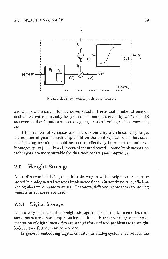
As noted in section 2.2.4, while for ease-of-writing the bias weight of neuron is usually included in the weighted sum of inputs (see section 1.1.1), in the case of a scalable hardware implementation special attention has to be paid to this weight. Here, the bias weight will be implemented separately with each neuron (in contrast with implementations where a synapse from the synapse array is selected and connected to a constant input source [Leh94, JCF96]). Figure 2.12 shows the elements of each neuron; a bias weight, a sigmoid block, and a summator to add the contribution of the bias weight to the input Sj-
A lower limit for the number of pins on each of the chips is given by:
in/ out addr ess+ WE supply ------- ,....,..__ PIN synapse = M + N + l og2 ( M · N) + 1 + 2
infout address+WE supply ~~,....,..__
PINneuron = 2 · M +log2(M) + 1 + 2
(2.17)
(2.18)
In equations 2.17 and 2.18 the major part of the pins is used for the inputs and outputs. Furthermore, a number of pins is used to address the· weights
2.5. WEIGHT STORAGE 39
refresh 1--------;.,. X • "-1" (V) (V)
Neuronj '----- -- - --- ------- ---- -------- - -------- -----------------_I
Figure 2.12: Forward path of a neuron
and 2 pins are reserved for the power supply. The actual number of pins on each of the chips is usually larger than the numbers given by 2.17 and 2.18 as several other inputs are necessary, e.g. control voltages, bias currents, etc.
If the number of synapses and neurons per chip are chosen very large, the number of pins on each chip could be the limiting factor. In that case, multiplexing techniques could be used to effectively increase the number of inputs/outputs (usually at the cost of reduced speed). Some implementation techniques are more suitable for this than others (see chapter 3).
2.5 Weight Storage
A lot of research is being done into the way in which weight values can be stored in analog neural network implementations. Currently no true, efficient analog electronic memory exists. Therefore, different approaches to storing weights in synapses are used.
2.5.1 Digital Storage
Unless very high resolution weight storage is needed, digital memories consume more area than simple analog solutions. However, design and implementation of digital memories are straightforward and problems with weight leakage (see further) can be avoided.
In general, embedding digital circuitry in analog systems introduces the

40 CHAPTER 2. SYSTEMS
need for converters from digital to analog. Using digital weight storage requires a digital-to-analog converter (DAC) in each synapse; the area of such converters typically scale as O(Q2) [Leh94], where Q is the resolution of the converter. In some cases, the converter and multiplier in a synapse are combined [LJ95, JCF96, dSPB+92, DET+92, MHW94, HP90, vdBFP+9o] saving some area but still the total implementation area is large.
For analog systems that include hardware learning, an analog-to-digital converter (ADC) is also required to be able to adjust the (digitally stored) weight values. In the case of parallel weight updating schemes [HPD91] such a system is area inefficient because of the necessary high weight resolution during learning [HF9l]. In [LBD94] , an elegant solution has been proposed by adding an analog adjustment to a digital memory. Weight changes determined by the on-chip learning algorithm are accumulated on the analog memory. When the equivalent of 1 LSB has been accumulated , the digital word is decreased or increased and the analog adjustment is reset .
2.5.2 Non-volatile Storage
The most popular of this kind of storage is the floating gate storage where a charge is trapped on the completely insulated (floating) gate of a MOS transistor [VOM+91, HN92]. There are various ways of trapping the charge on the floating gate [Ver94a]; some compatible with standard CMOS processes [LRIB96], other requiring special process steps as those in EEPROM processes [vHHW+93], for example.
There are several reasons why it is not preferable to use these kinds of memories in analog neural network implementations [Leh94]:
• Writing on these analog memories usually wears the devices. A typical floating gate devices can endure in the order of 10,000 full scale changes. This is sufficient for programmable recall-mode systems but for adaptive systems it is not.
• Digital electronics (RAM, microprocessors, etc.) are the driving force behind developing new VLSI technologies. State-of-the-art VLSI processes will be tuned to digital requirements and analog designers will only be able to use such processes if they are willing to use the possibilities offered by such processes.
• Even non-volatile analog memories compatible with standard CMOS processes should be used with caution: they rely on undocumented features of the process which (i) must be characterized experimentally,

2.5. WEIGHT STORAGE 41
(ii) probably are subjects to large process variations, and (iii) could possibly be changed without notice by the vendor.
2.5.3 Capacitive Storage
A very simple method for storing an analog signal is to put a charge on a capacitor and reading this using the high impedance gate input of a MOS transistor [TS87). A capacitor in MOS technology can be designed as a monolithic device using any structure in which a voltage-induced separation of charge occurs (passive structure) or using the gate oxide capacitance when aMOS transistor is operated in the non-saturated region (active structure) [Ver94a). The main drawback of the capacitive storage is that the leakage current (primarily) through the sampling switch eventually exhausts the weight. Several approaches to reducing the leakage are possible. However, most of these approaches e.g. [VOM+91] require a large implementation area.
Here, a simple differential scheme as shown in figure 2.13 will be used which cancels the influence of the source-bulk reverse biased junction currents (assuming both currents are equal) . Furthermore, this scheme also cancels, in first order, the offset errors due to charge injection through the sampling transistors. In a trade-off between retention time and area, capa-
Output
Figure 2.13: Differential capacitive weight storage
citors of 0.1pF are implemented and both sampling transistors are minimum sized. The capacitors are realized as a poly-poly structure. Weight values are stored by refreshing Vw2 with a constant voltage while the actual weight information is presented through Vw 1 • Both sampling transistors are operated simultaneously.
Weight decay cannot be totally eliminated with this kind of storage and

42 CHAPTER 2. SYSTEMS
some kind of refreshing scheme is necessary. Here an external digital RAM will store the weight values and the capacitors are periodically refreshed via an external D/ A converter [EDT89] in a serial fashion. More complex refreshing schemes are also known, see [Ver94a, HN92] for an overview. Although a capacitor is a true analog storage device capable of storing any value within a limited range["' 0; Vdd] (albeit for a short time due to leakage of the charge), here only a distinct number of values will be stored onto the capacitor. This is caused by the limited resolution of the digital RAM (typically 12-16 bit) and D/ A converter.

Chapter 3
lm plementation
The circuitry necessary to jill in the high-level schematics of both synapse and neuron chips in the previous chapter, will be presented here. T wo implementation approaches will be considered. A time-sampled, pulse stream implementation where analog values are encoded using binary signals and an analog, time-continuous implementation1 • In the latter case, a complete test system has been realized. Furthermore, a general comparison between the two approaches will be presented and high-level models for both synapses and neurons will be introduced.
3.1 Pulse Stream Approach
Because of the advantages they provide, pulse stream (PS) modulations [MCT91) are gaining support in the field of neural network hardware implementations. PS's are a class of modulation techniques widely used in other fields of electronics as well (e.g. telecommunications). They are based on "quasi-periodic" binary waveforms, where information is contained in the timing instead of the amplitude. Therefore, PS's are mainly used to encode analog values using binary signals.
Although pulse stream implementations were initially derived from studies on the behaviour of biological neurons and on the nature of elect rical spikes in axons, the reasons for a growing interest in such circuits is mainly due to their interesting characteristics and good computational performance.
1 ln principle, both the pulse stream and time-continuous approach presented in this chapter are analog implementations. However, here we will only refer to the timecontinuous approach as the analog implementation.
43

44 CHAPTER 3. IMPLEMENTATION
Here, first an overview of several well-known PS modulations and realizations of arithmetical functions using PS modulations will be presented in section 3.1.1 and 3.1.3, respectively. From the large number of modulation techniques, Coherent Pulse Width Modulation (CPWM) will be studied further. A theoretical analysis of CPWM and a general comparison between CPWM and analog multipliers are presented in section 3.1.2 and 3.1.4, respectively. In section 3.1.6 several CPWM building blocks including measurements on realized circuits are presented.
3.1.1 Overview of Pulse Stream Modulations
In neural network implementations, PS's are primarily used to encode input and output signals ai. In some cases, weight values are also coded as pulse streams. Here, several well-known PS techniques will be discussed [Rey95]. Figure 3.1 shows examples of timing for the PS techniques described below:
1. Pulse rate modulation (PRM) (also called pulse frequency modulation (PFM)[MT94]) pulses usually have constant width Ton while the average frequency of the PRM signal is proportional to the activation value:
(3.1)
where ai E [0 ... 1]. Typical values of !max used in the literature range from 500kHz to 5 MHz [Rey95]. With this technique, only the average frequency should be considered.
2. Pulse width modulation (PWM) pulses may have a constant frequency fo = A, while the widths of the individual pulses are proportional to the activation value:
(3.2)
where ai E [0 ... 1] and T max ~ To. Typical values of fo range between 100 kHz and 500 kHz. Pulse frequency does not need to be constant since the only relevant information is contained in the width .
3. Pulse code modulation (PCM) is a sequence of bits that the represent the binary encoding (i.e. in serial form with bit-rate fa) of the activation value. Bits are grouped together to represent a value with certain accuracy.

3.1. PULSE STREAM APPROACH
Ton ---1------1---
PRM _IlL__ __ nL__ __ n'--------
PWM
PCM
SPM 1 1
Td
PDM ___f1 n n n__ 1/fs 1---l
PBM
PAM _____n __ ___,n
Figure 3.1: Overview of PS modulations
45
4. The bits in a Stochastic pulse modulation (SPM) stream have an average bit rate /q = i: . The probability Pi ( 1) of having a "1" in the
q
sequence is proportional to an activation value:
(3.3)
where G'i E [0 ... 1].
5. With pulse delay modulation (PDM), the time Td between two pulses on either a pair of lines (called pulse phase modulation (PPM)), or on the same line is a function of the activation value.
6. With burst modulation (PBM), the number of pulses contained in a relatively short burst represents the activation value:
(3.4)

46 CHAPTER 3. IMPLEMENTATION
where I< N is a proportionality factor which gives the maximum number of pulses in each burst and ai E [0 ... 1] . Within bursts, fB is the peak bit rate.
7. Although Pulse amplitude modulation (PAM) is not a binary modulation technique, it is mentioned here since it is often used for neural computation in conjunction with other PS modulations. The pulse amplitude can be made proportional to the activation value.
A more elaborate overview of PS modulations including a performance analysis of the different techniques can be found in [Rey95).
3.1.2 Coherent Pulse Width Modulation ( CPWM)
Coherent Pulse Width Modulation (CPWM) is a variation of PWM, where all incoming streams have a known phase relationship with each other. As shown in figure 3.2, there is an additional reference clock (CCK) common to the whole system. CPWM activation signals (X1 .. . XN) have a constant
To Tmax ~idle ' '
active ' ' '
CCK~ IT11 w u u L
' . '
x1
XN
Figure 3.2: Timing diagram of CPWM modulation
frequency fo = A, while their width is proportional to the activation value:
1 + ai Ti = T maxai or Ti = T max -
2- (3.5)
for unilateral or bilateral CPWM, respectively. Activation values ai are normalized so that ai E [0 ... 1] or ai E [-1. .. + 1], respectively, while Tmax < To. Note that in the case of bilateral CPWM, the pulse width for an activation value ai = 0 is ~-
The reference clock defines two phases: CPWM signals are allowed to be "1" only during the active phase (Ti ~ T max) and they must always be

3.1. PULSE STREAM APPROACH 47
"0" during the idle phase. It is often convenient to avoid having Ti = 0 and Ti = Tmax, since (in certain circuits) this condition can increase the influence of charge injection effects, decreasing the overall accuracy of the system. Pulses are usually centered within the active phase2 . In both measurements and simulations reported here, fo = 1 MHz, T max = 800 ns.
Since a CPWM system is a time-sampled system, it may suffer from aliasing problems when dealing with time-continuous input signals which have to be processed by the system. Therefore a CPWM Nyquist frequency is defined as:
(3.6)
which is a parameter comparable to the cut-off frequency of analog systems. It will therefore be used to compare the performance of CPWM systems with the performance of analog ones (see section 3.1.5).
In spite of what was earlier believed [HMB+92], the phase relationship of CPWM streams does not imply synchronism among leading or trailing edges of the waveforms, which would cause high current spikes on the power supply. Assuming all activation values have an equal probability of occurrence and pulses are centered, waveform edges are uniformly distributed within the active phase of the reference clock [CV93, RCCG93].
Implementation Connections Response Power System Size per second Time Dissipation
(1.5pm CMOS) (per chip, 50mm2) (per synapse)
(x103 pm2) (x106 s- 1
) (ps) (pW) CPWM 5- 20 100 - 500 5- 10 10 - 100 PWM 5- 50 5- 50 50- 200 10 - 1,000 PRM 10 - 100 2- 20 ~ 100 100- 1,000 SPM 10- 30 25 - 100 20- 100 100- 200
Table 3.1: Performance comparison of several PS techniques
In [Rey95], both theoretical and real performance figures have been compared for different types of PS, showing that CPWM offers better performance than many others. Table 3.1 from [Rey95] shows a performance com parison for several important characteristics of different types of PS techniques. For each technique, a wide range of values is given since performance very much depends on the topology of the implemented neural network and on the specific circuit implementation of the different building blocks.
2 Left or right alignment within the active phase is also possible . However, the coincidence of either leading or trailing edges of the waveforms results in high transient CW'rents, which are undesirable.
48 CHAPTER 3. IMPLEMENTATION
3.1.3 Pulse Stream Arithmetic
Here, the implementation of several arithmetical functions using PS techniques will be mentioned. The list is not meant to be exhaustive but illustrative.
Addition
For PRM, addition could be simply realized by a logical OR function of two PS signals. If two pulse streams are uncorrelated, the logical OR of those signals will represent the addition of the two inputs. Errors are, however, introduced as the pulses in the two streams could overlap. If the two inputs streams are statistically independent, the overlap is a stochastic occurrence. In [MT94], an in-depth analysis is done on the occurrence of these errors related to size of a network. The technique of ORing signals together does not scale very well and is therefore not usable for large networks.
Multiplication
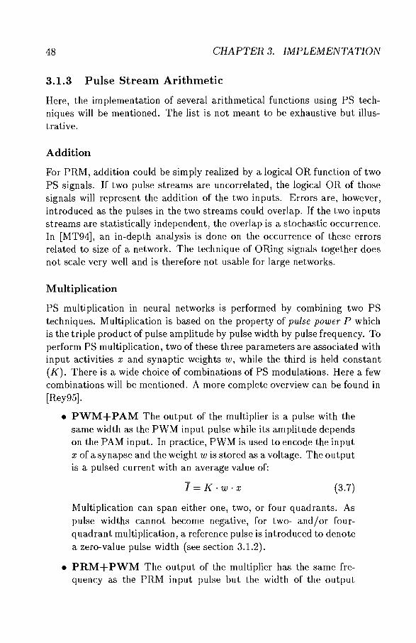
PS multiplication in neural networks is performed by combining two PS techniques. Multiplication is based on the property of pulse power P which is the triple product of pulse amplitude by pulse width by pulse frequency. To perform PS multiplication, two of these three parameters are associated with input activities x and synaptic weights w, while the third is held constant (K). There is a wide choice of combinations of PS modulations. Here a few combinations will be mentioned. A more complete overview can be found in [Rey95].
• PWM+PAM The output of the multiplier is a pulse with the same width as the PWM input pulse while its amplitude depends on the PAM input. In practice, PWM is used to encode the input x of a synapse and the weight w is stored as a voltage. The output is a pulsed current with an average value of:
(3.7)
Multiplication can span either one, two, or four quadrants. As pulse widths cannot become negative, for two- and/or fourquadrant multiplication, a reference pulse is introduced to denote a zero-value pulse width (see section 3.1.2).
• PRM+PWM The output of the multiplier has the same frequency as the PRM input pulse but the width of the output
3.1. PULSE STREAM APPROACH
pulse is modulated by the other input. The width of the output pulse is stretched or compressed in time to realize a multiplicative relationship.
• SPM+SPM Multiplication of two SPM streams can be achieved by a logical AND of the two inputs signals. Provided that the two streams are uncorrelated, the output is also a SPM sequence with probability Poutput(l) = x1x2 , where P1(l) = x1 and P2 (1) = x 2 are the probabilities for each input.
Hamming Distance
49
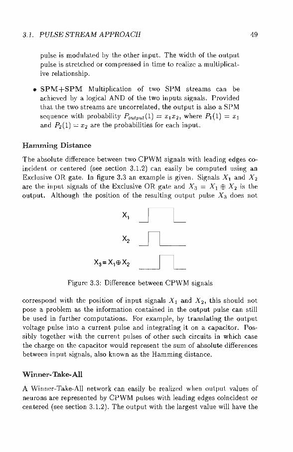
The absolute difference between two CPWM signals with leading edges coincident or centered (see section 3.1.2) can easily be computed using an Exclusive OR gate. In figure 3.3 an example is given. Signals X 1 and X 2
are the input signals of the Exclusive OR gate and X 3 = X 1 EB X 2 is the output. Although the position of the resulting output pulse X 3 does not
x,~
X2 Jl__
X3 =X1 ~X2 _Sl_ Figure 3.3: Difference between CPWM signals
correspond with the position of input signals X 1 and X 2 , this should not pose a problem as the information contained in the output pulse can still be used in further computations. For example, by translating the output voltage pulse into a current pulse and integrating it on a capacitor. Possibly together with the current pulses of other such circuits in which case the charge on the capacitor would represent the sum of absolute differences between input signals, also known as the Hamming distance.
Winner-Take-All
A Winner-Take-All network can easily be realized when output values of neurons are represented by CPWM pulses with leading edges coincident or centered (see section 3.1.2). The output with the largest value will have the

50 CHAPTER 3. IMPLEMENTATION
longest pulse and finding this signal in a collection of pulse width signals can easily be done using simple digital logic circuits. In figure 3.4 an example
X1 _fl__
X2 ___jL
x3 _11_ Figure 3.4: Winner-Take-All
is given with three signals X 1, X 2 , and X 3 • It is easy to see that signal X 2
is the winner. For the Winner-Take-All network to function properly, the rising edges of the input pulses should coincide.
3.1.4 Performance Analysis of CPWM Systems
This section presents a theoretical performance analysis of CPWM neural systems [RWHC94]. The results are later (see section 3.1.5) used to compare the performance of CPWM and analog systems. A multiplier is considered as the case study, although similar analyses can be applied to other parts of the system. To be able to compare both implementation schemes in a sensible way, the Gilbert cell [Mea89] shown in figure 3.5 will be used for both multiplication schemes3
. The differential output current of the Gilbert multiplier is converted into a single-ended current through a two-transistor current mirror and an output voltage is obtained by integrating the current during the active phase of the reference clock. Necessary simulations have been done using ES2 l.Of.Lm, double metal, single poly CMOS technology process parameters for typical parametric mismatches due both to variations b.f3 of the technological parameter f3 = fLoC ox~ and variations b. Vr of the threshold voltage Vr of MOS devices[AH87]. For both tail currents, mismatches in the aspect ratio ~ (b.W = ±0.25f.Lm, b.L = ±0.25f.Lm) and threshold voltages Vr (b. Vr = ±20m V) were introduced in a worst case combination.
The input-output characteristic of a multiplier is approximately4 given
3 Note that the Gilbert multiplier is quite similar to the CPWM multiplier proposed in [RCCG93].
4 Non-linearity in the multiplication is not included in this simple model and is studied separately.

3.1. PULSE STREAM APPROACH 51
Figure 3.5: Gilbert/CPWM multiplier
by:
(3.8)
where g is the multiplier gain, X 1 and X 2 are the two inputs, both normalized in the range [ -1 ... + 1], and 81 and 82 are the input offset terms for each input, respectively. The term 8M is the undesired output offset.
In the case of a CPWM system, one of the inputs is a CPWM signal, while the other one usually is a voltage. Here, X 1 is the CPWM input, with vl+ the pulse stream input and vl- the inverse pulse input. x2 is a differential continuous voltage; V2 = V/ - V2-. Vo is the output voltage of the multiplier, stored on a capacitor and sampled at the end of the active phase. Vo is normalized so that, for an ideal multiplier (.6.Vr = 1}.(3 = 0), g=l.
Multiplication errors
Errors are given by the sum of two major components, namely analog errors due to those transistors (called analog) operated in an analog fashion (i.e. linear or saturated region, e.g. M3, M4 , M5 , and M6 in figure 3.5) and digital errors due to those transistors (called digita~ which are operated as ON/OFF switches (e.g. M1 and M2 in figure 3.5).
In the case of the Gilbert multiplier, analog transistors are connected as a differential pair. Non-ideal devices and parametric spreads (1}.(3 and /}. Vr) cause that the weight-voltage to current characteristic differs from the desired one and therefore they introduce errors in the multiplier characteristic. Digital errors are given by timing errors (e.g. limited rise and fall times of

52 CHAPTER 3. IMPLEMENTATION
digital signals), by charge redistribution, and charge injection effects during switching of MOS-transistors.
Errors can be of three types, namely gain and offset errors and nonlinearities:
• Gain errors are due mainly to analog transistors. Gain is a function of both the Nyquist frequency fN (and consequently fa) and the mismatches among transistors. The gain is usually constant at low frequencies, while it reduces at higher frequencies. In the example shown in figure 3.5, there are two capacitively-charged nodes which produce two poles at about the same frequency (see figure 3.8):
9o(b.{3, b. VT) g-:::::, 1+(~)2 (3.9)
where fp and g0 are, respectively, the multiplier cut-off frequency and the low-frequency gain, which is a function of the mismatches !J.f3 and !J.VT (heuristic model). Table 3.2 gives the values of g0 and fp, as obtained from simulation of the case study.
• Input offset errors 8 1 and 82 can be handled independently. Variations in either f3 or VT have very little influence on input X 1 as only digital pulses are applied to this input. Analog input X 2 is influenced by both !J.f3 or !J.VT. However, this concerns the weight value input of the multiplier and any offset in this input can easily be compensated by a learning algorithm .
• Output offset errors eM have two components, which are due to analog (8A) and digital (8n) transistors, respectively. Since the two components are independent, they sum up together:
(3.10)
As for gain errors, the analog offset 8 A depends on transistor mismatches !J.f3 and b. VT but it is roughly independent of the clock frequency. On the other hand, digital offset 8 D is caused by charge injection due to switching of digital input signals. It is likely that a fixed quantity of charge is injected at every transition. Even though the charge due to rising and falling edges partially compensate, there is a net charge Ke injected at every input pulse, which causes an offset at the output. Therefore the digital offset is a function of the Nyquist frequency:
(3.11)

3.1. PULSE STREAM APPROACH 53
Simulations confirm this behaviour, as can be seen in figure 3.9. Table 3.2 presents the values of 8A and Ke, as obtained from simulations. It can be seen that the value of 8 A depends only on b..f3 and b.. Vr, while I<e is roughly independent of transistor mismatches.
Similar to offset in the weight input X2, offset in the output of the multiplier can easily be compensated for by the learning algorithm in conjunction with the bias weight of the neuron this multiplier will be connected to. However, as a large number of multipliers might be connected to the same neuron, care must be taken that the output offset of each multiplier is minimized to prevent the bias weight from becoming saturated.
• Non-linearity L: although a multiplier is by definition a non-linear system, it should behave partially linearly, in the sense that both the Vo vs. XI for a given value of x2 and the Vo vs. x2 for a given value of X 1 should be linear relationships.
A non-linearity factor L can be defined as:
f (Vo(Xt) - V0(Xt)) 2 dX1
f (V0(Xt)) 2 dX1 (3.12)
where V0(Xt) is the linear relationship which best fits Vo(X1). It is difficult to develop a theoretical model of the non-linearity but it is clear from simulations (see fig 3.10) that it depends on the Nyquist frequency in a rather irregular way.
In the case of a CPWM multiplier the analog-input to output relationship (e.g. Vo vs. X2 in the case study) is often non-linear, since it relies on non-linear devices (e.g. a differential stage in the Gilbert multiplier). Furthermore it should be comparable to that of an analog multiplier based on similar circuits (see figure 3.7) .
On the other hand the digital-input to output relationship (e.g. Vo vs. X 1 in the case study) is more linear, since it relies on an integration in the time domain, which is intrinsically a linear operator. In practice, VLSI capacitors are slightly non linear devices, therefore they reduce overall linearity.
Note that any non-linearities in the weight-to-output (in this case Vo vs. X 2 ) relationship of a synapse can be compensated by a non-linear weight updating scheme in the learning algorithm. Therefore, most
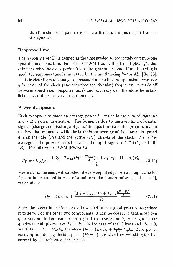
54 CHAPTER 3. IMPLEMENTATION
attention should be paid to non-linearities in the input-output transfer of a synapse.
Response time
The response time Ts is defined as the time needed to accurately compute one synaptic multiplication. For plain CPWM (i.e. without multiplexing), this coincides with the clock period To of the system. Instead, if multiplexing is used, the response time is increased by the multiplexing factor MR [Rey95].
It is clear from the analyses presented above that computation errors are a function of the clock (and therefore the Nyquist) frequency. A trade-off between speed (i.e. response time) and accuracy can therefore be established, according to overall requirements.
Power dissipation
Each synapse dissipates an average power Pr which is the sum of dynamic and static power dissipation. The former is due to the switching of digital signals (charge and discharge of parasitic capacitors) and it is proportional to the Nyquist frequency, while the latter is the average of the power dissipated during the idle (PI) and the active (PA) phases of the clock. PA is the average of the power dissipated when the input signal is "1" (Pt) and "0" (Po). For bilateral CPWM [RWHC94]:
0 E J (To- Tmax)PI + ~((1 + Cii)Pl + (1- Cii)Po) rr = 4 0 N + To , (3.13)
where Eo is the energy dissipated at every signal edge. An average value for Pr can be evaluated in case of a uniform distribution of ai E [ -1 ... + 1], which gives:
(T. T )p T (P,+Po) Pr = 4EofN + 0 - max I+ max 2
To (3.14)
Since the power in the idle phase is wasted, it is a good practice to reduce it to zero. For the other two components, it can be observed that most two quadrant multipliers can be redesigned to have Po = 0, while good four quadrant multipliers have P1 = Po. In the case of the Gilbert cell PI = 0, while pl = Po = vddlo, therefore Pr = 4EofN + TT~x vddlo. Zero power consumption during the idle phase (PI = 0) is realized by switching the tail current by the reference clock CCK.

3.1. PULSE STREAM APPROACH 55
3.1.5 Performance Comparison of CPWM and Analog Multipliers
The Gilbert cell of figure 3.5 will be used in simulations to be able to compare both static and dynamic behaviour for both computation schemes.
Simulations have been done for mismatches in the aspect ratio {3 (~ W = ±0.25~tm, ~L = ±0.25~tm) and threshold voltages Vr (~ Vr = ±20m V) introduced in a worst case combination. Like in the case of CPWM, analog inputs are normalized such that the linear range of the analog multiplier corresponds to a range [ -1 ... + 1].
The differential output current of the Gilbert multiplier is converted into a single-ended current through a two-transistor current mirrorfor both cases. For CPWM, this current is integrated using an ideal integrator and the resulting output voltage Vout is sampled at the end of the active phase, while for the analog system an ideal current-to-voltage converter is simulated and its output voltage represents the output of the multiplication.
Static comparison
First the static characteristics of the two multiplication schemes are compared. In the CPWM case, the relationship between the pulse input V1 and
0.8
0.6
0.4
0.2
o r-----------~~------------4
-0.2
-0.4
-0.6
·0.8
Figure 3.6: Static characteristic of CPWM multiplier for the pulse input for different values of v2,
for Io = 1ftA, ~{3 = ~ Vr = 0.
the output voltage Vo is in principle linear because it relies on the integration of a current on a capacitor. Figure 3.6 shows the Vo - V1 characteristic of a

56 CHAPTER 3. IMPLEMENTATION
CPWM multiplier for different values of V2• The relationship between both inputs and the output for the analog case has a similar shape. A sample plot is shown in 3.7 on the left side for the ideal case, i.e. without any mismatches. Furthermore, the Vo vs. V2 characteristic for CPWM also has this shape as it relies on the 'analog' behaviour of the Gilbert cell. Mismatches among
- 1 -~,L.s -~-.o~ .• --o~----:':o.,,-----~--::' .. , Nonn.bltd i"4l'Ut volta;• ol V1
t::J./3 = t:J.Vr = 0
& 9
l
i j
...
0 .5
.0.5
-o.5 0 0.5 NOfmaliudinputvoh• V1
Worst case mismatches
Figure 3.7: Static characteristic of analog multiplier for input vl for different values of v2
transistors caused by variations in the aspect ratio (3 and variations in the threshold voltages Vr, mostly result in a shift of the static characteristic of the multiplier for both multiplication schemes. A sample plot, where both mismatches are present in a worst case combination is shown in figure 3.7 on the right side.
Clearly, CPWM has an advantage with respect to the linearity between the output and the pulse input while the relationship between the continuous input and the output has a shape similar to the characteristics of the analog case.
Dynamic comparison
For the dynamic properties, gain, offset, and linearity as a function of frequency have been compared. Simulations have been done with different mismatches introduced.
• The gain versus frequency relationship of both the CPWM and the analog multiplier with 10 = lpA are shown in figure 3.8 for the ideal case, i.e. without mismatches. In the plot, the gain is normalized so that the gain at low frequencies is equal to 1. Both multipliers have a comparable bandwidth. Note that for the CPWM case, the Nyquist frequency is used in the plot.

3.1. PULSE STREAM APPROACH
0
-10
iii" ·20 :E!. c:
"iii C> -30 ., .~ Oi -40 E 0 z
-50
-60
-70 0.001 0.01 0.1 1 10 100
Frequency (MHz)
Figure 3.8: Gain vs. frequency relationship of analog and CPWM multipliers, for Io = lJ1A, 6.(3 = 6. Vr = 0.
I ., -~ Oi E 0 z
0.1
0.01
0.001
0.01
c~:J~~:~~,N~ := _.--CPWM simulated • ,././/_..~
/_Y/f
____ ......... ---·~·
0.1 1 Frequency (MHz)
.... --· ,<
10 100
Figure 3.9: Offset vs. frequency relationship of analog and CPWM multipliers, for 10 = lJ1A, 6.(3 = 6. Vr = 0.
57
• Figure 3.9 shows the offset as a function of the frequency for both CPWM and analog multipliers in the ideal case. In the analog case, for frequencies higher than lMHz, the offset increases due to capacitive coupling, while for even higher frequencies both the signal and offset are heavily attenuated5 . For CPWM, offset for low frequencies is higher than in the analog case and increases for high frequencies. This
5 The values for e A collected in table 3.3 are valid for the low-frequency range where the offset is constant.

58 CHAPTER 3. IMPLEMENTATION
is mainly due to capacitive coupling between the pulse input (with high frequency components due to the pulse shape) and the output. Both theoretical and simulation points are shown for the CPWM multiplier. Note that the behaviour above the cut-off frequency is not so important for the functioning of the multiplier.
-~
i i:. 0 z
0.1
O.DI / ..• /;
------ ·---------· ·-------./
0.1 1 Frequency (MHz)
Analog simulated --CPWM simulated ·•···
10 100
Figure 3.10: Non-linearity vs. frequency relationship of analog and CPWM multipliers, for fa = 1J.LA, /::if]= l::i Vr = ; 0.
• The dynamic non-linearity of both multiplication schemes has been compared in the following way. An AC source was connected to input V1 while a DC sweep (over the complete input range) was made with the voltage connected to V2. For each frequency of the AC source, a best linear fit was made for the output voltage and the non-linearity factor was computed, as defined in formula 3.12. The results of the simulations are shown in figure 3.10, where it can be seen that for low frequencies CPWM linearity is much better. The linearity of the analog multiplier is better around 10 MHz but as this is higher than the cut-off frequency, it is not so interesting.
Data on gain, cut-off frequency and offset are collected m tables 3.2 and 3.3, for both multiplication schemes.
Conclusion
From the simulations and analyses presented above, it may be concluded that both computation schemes have a comparable performance for low power consumption values. Bandwidth is slightly in favor of analog systems,

3.1. PULSE STREAM APPROACH
lo Mismatch 9o /p E) A I<e pA MHz MHz- 1
1 - 1.00 2.1 0 .006 0.059 1 6.{3 0.76 2.1 0.158 0.042 1 IJ.VT 0.84 2.1 0.105 0.049 1 6.{3 + D. VT 0.55 2.3 0.278 0.031
Table 3.2: Typical parameters for a CPWM multiplier Data extracted from simulations [RWHC94].
lo MISMATCHES 9o fp E) A
pA MHz 1 - 1.00 3.5 0.002 1 6.{3 0.79 3.5 0.126 1 IJ.VT 1.08 3.7 0.068 1 6.{3 + D. VT 1.41 3.6 0.263
Table 3.3: Typical parameters for an analog multiplier. Data extracted from simulations [RWHC94] .
59
while non-linearity is slightly in favor of CPWM systems. For higher values of power consumption , analog systems have a more distinct advantage in bandwidth [RWHC94]. Nevertheless, CPWM systems have some additional advantages:
• Design of CPWM systems is less complicated, since several devices are operated as ON/OFF switches reducing their sensitivity with respect to process variations (e.g . .6. VT).
• Multiplexing and handling (e.g. routing) of CPWM signals is easier as it can be performed by digital circuits (e.g. multiplexers) [Rey95].
• The noise sensitivity of CPWM systems is much lower than that of analog systems [RWHC94].
Note that most multipliers reported in the literature [GSBJ91] have been designed with a much higher power consumption than their CPWM equivalents (see [Rey95] for detailed analysis).
3.1.6 Building Blocks
Here, the building blocks necessary to fill in the high level schematics of both synapse (section 2.4.1) and neuron (section 2.4.2) will be introduced for the

60 CHAPTER 3. IMPLEMENTATION
pulse stream implementation. Most blocks have been implemented on a chip containing several test structures6 .
One-quadrant Multiplier
A simple one-quadrant CPWM multiplier can be realized with only two transistors, as shown in figure 3.11. A continuous voltage Yin; is applied to transistor M1, while the pulse stream signal Xi is connected to transistor M2 which operates as a switch. As long as transistor M1 is operating in the linear region, the output current Iout; has a linear relationship with the input voltage Yin;. Keeping M1 in the linear region can be accomplished by leading the output current through a current conveyor in which case the voltage over the multiplier can be kept constant. To obtain a multiplicative
Figure 3.11: One-quadrant CPWM multiplier
relationship between the two inputs, the output current I out is used to charge a capacitor Cint, according to:
1 1Tmax J< Vout; = c----:- Iout;(t)dt = -C· (Yin;- VT)Ti
tnt 0 2 tnt (3.15)
where Ti is the pulse width of the CPWM signal present at input Xi, while the capacitor voltage Vout represents the multiplier output. I< is a factor which includes the transconductance and the (constant) drain-source voltage of Ml. During the idle phase the capacitor is discharged.
Two-quadrant Multiplier
Figure 3.12 shows a two-quadrant multiplier consisting of a Voltage-toCurrent Converter (VCC), realized with transistors M1 through M5, of
6 Currently, work is going on to implement a complete synapse array using the MIETEC 0.5pm double poly, triple metal process.

3.1. PULSE STREAM APPROACH 61
which the power supply is switched through M6. One input of the multiplier is a differential continuous voltage Vw; = Yin; - Vref which is used to represent the weight in a synapse. The input Xi is a ePWM signal, usually
Figure 3.12: Two-quadrant ePWM multiplier
the input signal to the synapse. The continuous input is bilateral , while the pulse input is unilateral. Hence, the output current l out is a pulsed current which can either have a positive or negative sign resulting in a two-quadrant multiplication.
As for the one-quadrant multiplier, the output current lout is integrated on a capacitor7
:
(3.16)
with Ti = Tmaxl:Xi, <:Xi E [0; 1] (unilateral), Vw; = VwmaxWi, Wi E [-1; 1] (bilateral), and K the transconductance of the vee, respectively.
7 lt assumed here that the vee is ideal in the sense that the output current has a linear relationship with the input voltage.

62 CHAPTER 3. IMPLEMENTATION
Figure 3.13 shows the measured characteristics of the two-quadrant multiplier realized in the MIETEC 2.4 J-Lm double-poly, double-metal process (additional circuit details can be found in appendix D). As the output of the multiplier is a pulsed current (which is difficult to measure), the complete transfer of both multiplier and integrator (see below) has been measured8 .
The output vs. weight characteristic is measured for different pulse widths covering the whole pulse input range and similarly, for the output vs. pulse plot weight voltages from -1V to +1V were used. As mentioned in section 3.1.2, Ti = 0 and Ti = Tmax are avoided to minimize the influence of charge injection.
2.5
f J 15
0.5
-0.5 0 0.5 Weigh1vol1ag1 M
Output vs. Weight
2.5
f i 15 0
0.5
0 oL-~100~~=~~~~~=~~~~~~~~,oo~~ Pul•• widlh in n•
Output vs. Pulse
Figure 3.13: CPWM characteristics (measurement)
Taking into account the simplicity of the synapse circuit, the plots show excellent linearity both for the pulse-to-output as well as the weight-tooutput transfer characteristic. A more non-linear behaviour of the latter might not have been a problem as this can be compensated by the (nonlinear) weight updating scheme in the learning algorithm.
The photograph in figure 3.14 shows the realized two-quadrant CPWMmultiplier including capacitors for weight storage and access transistors for refreshing. The area occupied by the multiplier (excluding the capacitors and access transistors) amounts to 3700J-Lm2. An estimate for a complete synapse (including capacitors, access transistors, address decoding, and communication lines) in the same 2.4J-Lm technology amounts to 14,000J-Lm2•
It should be noted that the power consumption of the multiplier is low. The bias current is as low as 10 J-LA and this current is only flowing when transistor M6 is conducting. Hence, the synapses will not consume any power
8 Each dot in the plots represents the output voltage of the integrator at the end of the active phase.

3.1. PULSE STREAM APPROACH 63
Figure 3.14: Photograph of realized ePWM-multiplier
during the idle phase of the clock period and power consumption during the active phase is depending on the pulse signal input. Assuming that on average the ePWM input Xi of the multiplier during the active phase is" 1" in 50% of the cases, the average power dissipation P2q = T!f\;* ·0.5·hias· Vdd = 0.8 · 0.5 · lO~tA · 5V = 20~tW.
Special care should be taken during layout of ePWM building blocks as both analog and digital signals are used in almost all blocks. Especially, digital signal lines should be shielded to minimize the influence (e.g. via the substrate and capacitive coupling between signal lines) of high-frequency components in the ePWM signals on analog voltage levels and microamp current levels. Furthermore, standard layout techniques [Ver95b, Ver95a) used in mixed analog-digital circuit design should be applied. At the cost of some increased implementation area, significant improvements in accuracy of the total system can be achieved.
Four-quadrant Multiplier
The two-quadrant multiplier of figure 3.12 can easily be expanded to a fourquadrant multiplier. As can been seen in figure 3.15 only 4 switches (M7-M10) are added to the original circuit. In this case, the power supply of the vee is switched by the inverse of the reference clock (eeK) and the weight voltage Vw;(= Vin;- VreJ) is switched between the inputs (M1 and M2) of the vee by the ePWM input signal Xi. Both the continuous input and pulse input are bilateral hence realizing a four-quadrant multiplication.
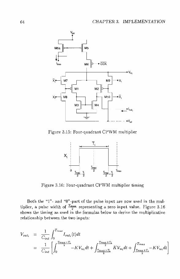
64 CHAPTER 3. IMPLEMENTATION
Figure 3.15: Four-quadrant CPWM multiplier
Tmax -2-
Figure 3.16: Four-quadrant CPWM multiplier timing
Both the "1"- and "0"-part of the pulse input are now used in the multiplier, a pulse width of ~ representing a zero input value. Figure 3.16 shows the timing as used in the formulas below to derive the multiplicative relationship between the two inputs:
Vout; C1 {Tma:r lout; (t)dt
mt Jo
[
Tma:r-Tj Tma:r+Tj T l 1 Ia 2 h 2 h ma:r -C -I<Vw;dt + T -T· KVw;dt + T T -KVw;dt · t 0 ma:r , max+ , •n 2 2

3.1. PULSE STREAM APPROACH 65
1 [1T; jTmax l -C· KVw;dt + -KVw;dt tnt o T;
(3.17)
where ai E [-1; 1] and Wi E [-1; 1). The four-quadrant CPWM multiplier has been simulated using the
MIETEC 2.4J.Lm process characteristics. To obtain a realistic simulation of such a dynamic circuit in silicon, a complete system, i.e. a multiplier and an integrator, has been simulated. Figure 3.17 shows the output versus
...
...
• .• L..---.~ •.• --~.---,.~ .• --...._j
Weightvolta~M
Output vs. Weight
too 200 300 400 500 eoo 100 aoo Pulu widtl in na
Output vs. Pulse
Figure 3.17: CPWM characteristics (simulation)
weight characteristic for different pulse widths and the output versus pulse width relationship for different weight values, respectively. As the circuit is basically the same as the two-quadrant multiplier plus some switches, the observed linearity is again very good.
In contrast with the two-quadrant multiplier, power consumption of the four-quadrant version is not dependent on the CPWM input signal but constant, P4q = Tl¥;x . hias. vdd = 0.8. 10J.LA. 5V = 40J.LW.
Integrator + Sample & Hold
The summing input of a neuron is realized by connecting the outputs of one or more multipliers, each generating a pulsed output current, together to

66 CHAPTER 3. IMPLEMENTATION
a low-impedance node. The resulting current is integrated on a capacitor and the voltage over the capacitor at the end of the active phase represents the sum of weighted inputs (see section 1.1.1). By realizing the integrator as a floating capacitor over an operational amplifier, a virtual ground input node is created. By connecting the outputs of several multipliers to this input
Figure 3.18: Integrator
node (common to all multipliers) of the integrator, summing is automatically realized and the characteristics of the multipliers are not influenced due to a constant voltage at the output of each multiplier. The inset in figure 3.18 shows the general schematics of the total circuit. The output voltage of the integrator at the end of the active phase is stored through a simple Sample & Hold circuit (M8 and C2). The stored voltage is used by subsequent circuits during the clock period following the current one. The circuit shown in figure 3.18 has been realized together with the two-quadrant CPWM-multiplier presented before. During measurements of the multiplier this circuit was used to transform the pulsed output current of the multiplier to an output voltage at the end ofthe active phase.
The switch operated by Vconnect is necessary to make sure that the integration capacitor C3 is completely cleared during the idle phase and no charge from any of the connected multipliers is accumulated before the active phase starts. The complete timing diagram of the different switches in figure 3.18 in relation to the CPWM reference clock is shown in figure 3.19. In practice, the reference clock CCK is directly connected to Vconnect.

3.1. PULSE STREAM APPROACH 67
active idle
CCK
vconnect
Vsample Jil ~ ' '
vdump Jl IL Figure 3.19: Integrator timing
Scaling
Scaling, as earlier introduced in section 2.2, should ideally be realized in a distributed way, i.e. the output current of each synapse should be automatically scaled when the network size increases. Examples of implementations of automatic linear scaling can be found in [CV93, STG92]. However, square root scaling (as derived in section 2.2) is difficult to realize in an area efficient way in a synapse. Therefore, a variable integration capacitor will be introduced at the integrator (C3 in figure 3.18). By realizing the integration capacitor as several separate capacitors in parallel with values in a relation 1:2:4:8 including some switches, a maximum scaling factor of 15 can be realized and from 1 to 225 synapses can be connected to the same neuron.
Sigmoid
The output of each neuron should again be a voltage pulse stream compliant with the CPWM timing, which can be distributed to several synapses. The integrator presented in the previous section realizes the summing input node of a neuron (see section 2.4.2). An additional block is necessary to implement the non-linearity and generate an output pulse stream which can be fed to a number of synapses. Two approaches will be considered:
• In the case of a static sigmoid implementation, the voltage stored on capacitor C2 in figure 3.18 is applied to a circuit which implements
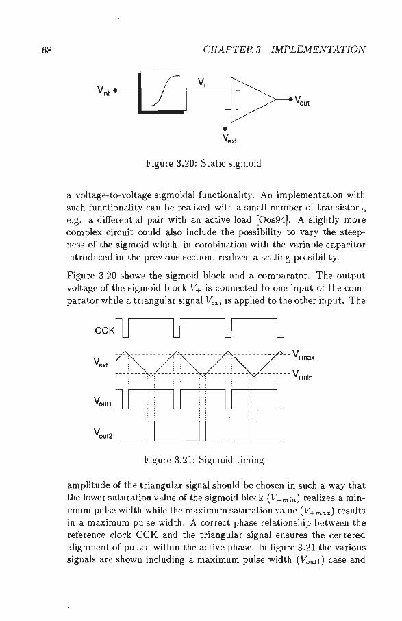
68 CHAPTER 3. IMPLEMENTATION
r v+ ~nt --------1 _} f--------1
Figure 3.20: Static sigmoid
a voltage-to-voltage sigmoidal functionality. An implementation with such functionality can be realized with a small number of transistors, e.g. a differential pair with an active load [Oos94] . A slightly more complex circuit could also include the possibility to vary the steepness of the sigmoid which, in combination with the variable capacitor introduced in the previous section, realizes a scaling possibility.
Figure 3.20 shows the sigmoid block and a comparator. The output voltage of the sigmoid block V+ is connected to one input of the comparator while a triangular signal Vext is applied to the other input. The
ccKlJ u u L vext - - : -------- - -- . - ------- - - - - : ---------- - . - -- v+max
---·---- - .-----·-·---- .-. - - --~--- v . : : +min
u U L vout2 _n._____.n._____jl_
Figure 3.21: Sigmoid timing
amplitude of the triangular signal should be chosen in such a way that the lower saturation value of the sigmoid block (V+min) realizes a minimum pulse width while the maximum saturation value (V+max) results in a maximum pulse width. A correct phase relationship between the reference clock CCK and the triangular signal ensures the centered alignment of pulses within the active phase. In figure 3.21 the various signals are shown including a maximum pulse width (Voutl) case and

3.1. PULSE STREAM APPROACH 69
a minimum pulse width (Vout2) realization.
• Dynamic waveform comparison is another way to realize the sigmoidal functionality. This approach combines the realization of the non-linearity and the generation of pulses. In this case, the output of the integrator Vint is directly connected to the input of the comparator while to the Vext input, a signal which represents the inverse of the sig-
CCKU u u L vext
. -- --- -- - -- - ---- --- - ---------- -- - --- -- -- - v+min
----------- - -- - - ------ -- --- -- ----- - - -- v+max
Figure 3.22: Dynamic waveform comparison
moidal function is applied, see figure 3.22. In this way, the resulting output pulse has a width which is dependent on the integrator output in a non-linear way. The shape, e.g. steepness, of the sigmoid can be easily adjusted as the signal is generated externally. Note that Vext only has to be generated once for the whole network in case all neurons in a network have the same sigmoid shape.
In this way, the neuron unit requires less implementation area and it consumes less power. Besides this, process parameters variations will have no influence on the sigmoid shape. One of the major problems with this approach is the high-speed generation of the Vext signal. Assuming Vext is generated through a D/ A converter from a digital memory, To = lMHz, and the number of samples per sigmoid segment is 64, the D/ A converter needs to run on a clock frequency of 128MHz! Another way to generate the inverse sigmoidal signal is depicted in figure 3.23. A triangular signal is applied to an operational amplifier across which a circuit is placed which realizes a sigmoidal characteristic between the output of the amplifier (Vext) and one of the inputs (V_) (e.g. a differential pair with an active load [Oos94]). The resulting output signal has the desired shape.
In both of the presented approaches, care should be taken that the comparator does not introduce an excessive delay. For small pulse widths this does not introduce any problems as pulses are just not completely centered any longer. However, in the case of a pulse width close to Tmax, the resulting output pulse could be distorted as part of the pulse 'shifts' into the idle

70 CHAPTER 3. IMPLEMENTATION
>-----'---V. .. ext ~
Figure 3.23:
phase of the reference clock. Careful design of the comparator should avoid input offsets and large delays in the case of a small differential input voltage (V+-V-).
3.2 Analog Implementation
Historically, digital implementations of neural networks, both dedicated fully parallel implementations [MDGS92] and software simulations on a digital computer (in principle a serial implementation in the case of a single processor machine), had the advantage of a high accuracy. Neural network paradigms could be studied in a well-controlled . environment. However, if rieural networks are to be implemented in a fully parallel architectu re, analog VLSI is required. In future , large parallel implementations should yield sufficient computational power to realize systems capable of human-like cognitive tasks (e.g. face recognition, speech recognition). Such large systems can only be implemented if building blocks are sufficiently small to implement tens of thousands on a single chip. Simple analog multipliers and other neural blocks can be implemented with only a few transistors at the cost of reduced accuracy. However, it is believed that a combination of the way information is stored in a neural network (distributed) and the learning algorithm used to obtain a certain functionality should ensure that the reduced accuracy does not pose a problem. In chapter 4, several learning algorithms in combination with analog hardware will be studied.
Here, first a short overview of earlier reported analog realizations will be given. In section 3.2.2 and 3.2.3 circuits to realize synapse and neuron functionality will be introduced, respectively. A complete test system will be presented in section 3.2.4.

3.2. ANALOG IMPLEMENTATION 71
3.2.1 Existing realizations
In recent years, a large variety of analog implementations of neural network has been reported. Here, several will be mentioned including some remarks. A more complete overview of both analog and digital neural network implementations can be found in [DEDT96].
With reference to the methods of weight storage (see section 2.5), several implementations combine digital storage with a multiplying digital-to-analog converter (DAC) [LJ95, JCF96, dSPB+92, vdBFP+go, DET+92, MHW94, HP90]. While delivering very good linearity, the implementation area is relatively large. In [LJ95] a complete low-power implementation of this kind is reported with bias-currents as small as 6.3nA.
In most cases, a lot of effort is put in realizing very linear multipliers at the cost of a large implementation area [STG92, CBS93, GLJ94, FSTCC92, FA88, HTCB89, THB+92]. As multipliers are the most used building blocks in neural networks, reducing their implementation size, influences the total implementation size of a network greatly. [LG92, LL93, Leh94] use multipliers consisting of only several transistors, at cost of reduced linearity.
The building-block approach [EDT89] where several chips can be interconnected to realize different network structures has proved popular. One of the implications of this approach (as mentioned in section 2.1), is that several parts of the implementation have to be able to handle a variety of conditions (e.g. a neuron with only 2 synapses connected and the same neuron with 64 synapses connected). Most implementations have some kind of scaling possibility built-in in the sigmoidal function of the neuron. However, in [MA94, LL95, CBS93, DET+92, EDT89, HP90] varying the steepness of the sigmoid also results in different saturation levels of the sigmoid , thereby reducing the effective input range of the multipliers in the next layer. In [MHW94, LL93] more robust implementations of the sigmoid can be found which do not exhibit this behaviour. In the case of [LL93], however, CMOS and bipolar techniques are mixed.
A very elegant solution to the problem of scaling can be found in [STG92] where neurons are implemented in a distributed way. With this implementation the main building block is a combined neuron-synapse circuit.
In [MHW94, MHW93], very high speed implementations are reported for specialized applications in high-energy physics.
In most of the above mentioned realizations, the majority of circuits are voltage-mode. Work on current-mode implementations of neural networks is reported in [CM93, NAS92, Nij95].
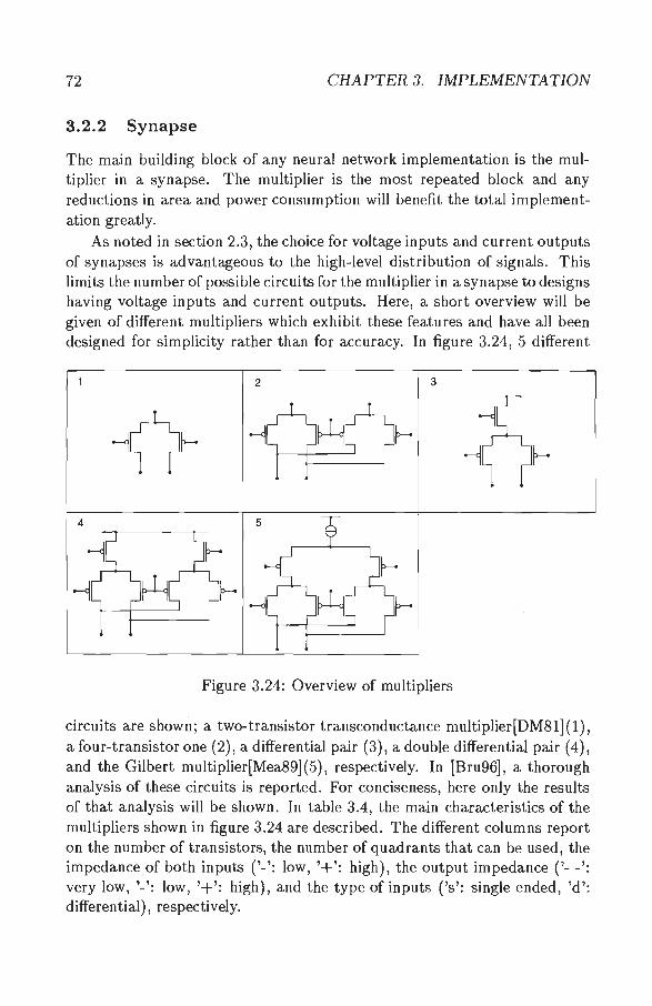
72 CHAPTER 3. IMPLEMENTATION
3.2.2 Synapse
The main building block of any neural network implementation is the multiplier in a synapse. The multiplier is the most repeated block and any reductions in area and power consumption will benefit the total implementation greatly.
As noted in section 2.3, the choice for voltage inputs and current outputs of synapses is advantageous to the high-level distribution of signals. This limits the number of possible circuits for the multiplier in a synapse to designs having voltage inputs and current outputs~ Here, a short overview will be given of different multipliers which exhibit these features and have all been designed for simplicity rather than for accuracy. In figure 3.24, 5 different
2 3
Figure 3.24: Overview of multipliers
circuits are shown; a two-transistor transconductance multiplier[DM81](1), a four-transistor one (2), a differential pair (3) , a double differential pair (4), and the Gilbert multiplier[Mea89](5), respectively. In [Bru96], a thorough analysis of these circuits is reported. For conciseness, here only the results of that analysis will be shown. In table 3.4, the main characteristics of the multipliers shown in figure 3.24 are described . The different columns report on the number of transistors, the number of quadrants that can be used, the impedanceof both inputs ('-': low, '+ ': high) , the output impedance ('- - ' : very low, '-': low, '+': high), and the type of inputs ('s ' : single ended, 'd': differential), respectively.

3.2. ANALOG IMPLEMENTATION 73
Circuit #T #quad Zin Zout m
1 2 4 -,+ - - s,d 2 4 4 -,+ - d,d 3 3 2 +,+ + s,d 4 6 4 +,+ + d,d 5 6 4 +,+ + d,d
Table 3.4: Overview of multiplier characteristics
The two-transistor and differential pair multiplier only need a few transistors and are therefore attractive for their small implementation area. Furthermore, both have one single-ended and one differential input. In a neural network implementation, a single-ended input of a synapse has the advantage of less communication lines between neuron and synapse chips and the differential storage of weight values reduces the complexity of the storage circuitry. However, while the differential pair multiplier has both high impedance in- and outputs, it can only be used as a two-quadrant multiplier. The other three multipliers all have two differential inputs. In two cases, this is combined with high in- and output impedances at the cost of additional transistors.
Although the two-transistor multiplier has some disadvantages (one low impedance input and a low impedance output), it offers the possibility to perform four-quadrant multiplication with only two transistors. Here, a synapse implementation based on the two-transistor multiplier will be pursued. First, the multiplier itself will be introduced and analyzed. Furthermore, additional circuitry, measurements on a realized synapse, and a synapse array chip will be presented.
Multiplier
Figure 3.25 shows the two-transistor multiplier. When both transistors M1 and M2 are working in their linear range, equations 3.18 and 3.19 apply for the direction of current shown in figure 3.25, i.e. Vz > Vyl and Vz > Vy2:
h = {31 { [(Vz- Vwi)- IVTII) (Vz- Vyl)- ~(Vz- Vyi) 2}
h = f32 { [(Vz - Vw2)- IVT21) (Vz - Vy2)- ~(Vz- Vy2) 2}
(3.18)
(3.19)
Assuming transistors M1 and M2 are equal (IVr1l = IVr2l = IVrpl and f3I = f32 = (3) and Vy 1 = Vy2 = Vy, the difference in current can be expressed

74 CHAPTER 3. IMPLEMENTATION
Figure 3.25: Two-transistor multiplier
as: (3.20)
Equation 3.20 shows a perfect multiplicative relationship between the inputs. The multiplier could be used in a synapse when Vz- Vy is used as input and Vw2 - Vwl as weight value. The output of the multiplier is the differential output current. Equations similar to 3.18 and 3.19for Vz < Vy can be written out, resulting in the same expression as equation 3.20, thereby realizing fourquadrant multiplication.
The following should be noted when using this circuit in a synapse:
1. The linearity of the circuit is good due to the fact that both transistors are assumed to be equal and working in their linear range. The voltages Vy 1 and Vy2 also have to be equal and constant (see equation 3.20). To keep the transistors working in their linear range, the voltage ranges of Vwl, Vw2, Vz, and Vy are chosen in the following way: 0::::; Vwl::::; lV, Vw2 = 0.5V, 2V ::::; Vz ::::; 3V, Vy = 2.5V, respectively. These values are valid for a realization in the MIETEC 2.4J.Lm double poly, double metal process which has a Vro = -0.85V for PMOS-transistors.
2. Power dissipation and implementation size of the multiplier can be exchanged. The currents in each of the branches can be tuned by adjusting the aspect ratio (W /1) of both transistors . Here, a compromise has been found by using transistor sizes of W / L = 4.8J.Lm/18J.Lm. In that case, currents in the 2 branches of the multiplier vary: -2.5J.LA < 11 < 2j.tA, -2J.LA < h < lj.tA and the resulting differential output current -800nA < It - h < 800nA. Power consumption of the multiplier depends on the input and weight values and ranges from OW (in case the multiplier is not used or Vz = Vy) to 2.25J.LW.
Figure 3.26 shows a photograph of the realized two-transistor multiplier including two capacitors for weight storage (see section 2.5), a

3.2. ANALOG IMPLEMENTATION 75
Figure 3.26: Photograph of realized two-transistor multiplier
NOR-gate for address decoding (see section 2.4.1), and communication lines for several signals. The complete structure of figure 3.26 occupies 12,880JLm2.
3. The linearity of the multiplier may be disturbed by the channel length modulation effect, indicated by A. Equation 3.20 changes into:
(3.21)
The quadratic term due to the channel length modulation will be small if A is small. In this case, as L is large, A is as small as 3.9e-3 and the effect will be negligible.
4. The threshold voltage Vr of a transistor is influenced by the body effect [AH87, Ver94b] in the following way:
Vr = Vro + 'Y [VI- 2¢F + VsBI- filM] (3.22)
The parameter 'Y is known as the body effect coefficient. The bodyeffect can be reduced by choosing VsB >==:::: OV. While for PMOS transistors VsB may not become positive, VB is chosen MAX (Vs) = MAX(Vz) = 3V.

76 CHAPTER 3. IMPLEMENTATION
Subtractor
The requirement Vy 1 = Vy2 = Vy for the circuit introduced in the previous section, can be fulfilled by implementing a current conveyor behind the multiplier [Bru93, Oos94] or a low input impedance summing amplifier [KMML90]. Both solutions have a large implementation area and high power consumption. Here, a straightforward subtraction implementation will be introduced. Giving up the requirement that the Vy-values should be equal and constant, it is possible to subtract the currents by using small resistors as loads which convert the currents to small proportional voltages. This devi-
I Figure 3.27: Multiplier load
ation from the ideal situation will cause the multiplier to become non-linear. However, if the voltage swing at the output nodes of the multiplier is kept small, the influence will be marginal. Furthermore, the loads can be shared by all synapses connected to the same neuron. This has two advantages:
1. Area reduction, because the subtraction circuit only has to be implemented once per column of synapses,
2. If the loads are tunable, a scaling possibility is introduced m the synapse chip.
Figure 3.27 shows the implementation of the load. It consists of two NMOStransistors, which when working in their linear range and VDs is small compared to (Vas- Vr), each realize a resistance of:
(3.23)
where KN is the transconductance of the NMOS-transistor. PMOStransistors are added in parallel to linearize the behaviour of the circuit9 •
9 See section 3.2.3 for a derivation of the behaviour of the load which is similar to the variable gain used in the neuron.

3.2. ANALOG IMPLEMENTATION 77
Vg ain can be used to adj~t the load to the number of synapses connected to it. The differential outpu~ voltage Vy 1 - Vy2 is converted into a single-ended
Vy1 +---------,-t- ----+----1
Multiplier i 11 l2 i - - - ---- -------- ------ ------ --- -·--- --- --
Load
r v,., Subtractor
Figure 3.28: Total Synapse
output current using a standard differential stage with a current mirror load (OTA).
Figure 3.28 shows the complete circuit consisting of the two-transistor multiplier (upper left), the tunable loads (lower left) shared between synapses, and the OTA (right) . In figure 3.29, measurements for the complete
· I
2.2 2.4 2 .8 -0.4 .() .2 0 02 0 .4 Input voltage Wtllgtllvollage
Output vs. Input Output vs. Weight
Figure 3.29: Synapse characteristics (measurement)
synapse are plotted for both output Uout) versus input (Vz) for different weight values and output versus weight (Vwl - Vw2) for different input val-
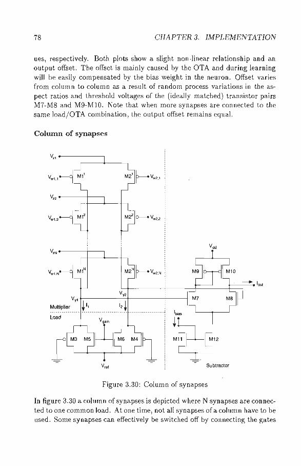
78 CHAPTER 3. IMPLEMENTATION
ues, respectively. Both plots show a slight non-linear relationship and an output offset. The offset is mainly caused by the OTA and during learning will be easily compensated by the bias weight in the neuron. Offset varies from column to column as a result of random process variations in the aspect ratios and threshold voltages of the (ideally matched) transistor pairs M7-M8 and M9-Ml0. Note that when more synapses are connected to the same load/OTA combination, the output offset remains equal.
Column of synapses
Figure 3.30: Column of synapses
In figure 3.30 a column of synapses is depicted where N synapses are connected to one common load. At one time, not all synapses of a column have to be used. Some synapses can effectively be switched off by connecting the gates

3.2. ANALOG IMPLEMENTATION 79
to the supply voltage (5V). Vgain can be used to adjust the output current level to the number of synapses used in one column (3.85V:::; Vgain :::; 5V). In the case of large synapse arrays, Vgain should be adjusted as described in section 2.2.
The implementation size of a column of 8 synapses (including load, OTA, and communication lines) realized in a 2.4J-Lm double poly double metal process measures 124,000J-Lm2
• The average size of 1 synapse then becomes 15,500J-Lm2
. Note, that this figure will decrease as more synapses are connected to the same common load in a larger array structure (e.g. 32x32 synapses). The size compares favorably to other reported synapse implementations [Leh94, MA94, dSPB+92, LG92] resulting in a synapse density of 64.5/mm 2.
Synapse array chip
The complete synapse array chip contains 8 columns of synapses with 8 synapses each, in total realizing an 8x8 fully connected synapse layer. By loading the appropriate weight set to the chip, an arbitrary number of synapses per
Figure 3.31: Photograph of 8x8 synapse chip
column can be used. In figure 3.31 a photograph of the realized synapse chip

80 CHAPTER 3. IMPLEMENTATION
is shown10• The complete size of the chip (7.61mm2) is mainly determined by the number of input- and output pins. This number will be reduced in future designs by generating necessary bias voltages and currents on-chip.
3.2.3 Neuron
The main property of a neuron is the non-linear, saturating function which is applied to the input of the neuron . A complete neuron could be realized as
Figure 3.32: Neuron implementation
depicted in figure 3.32, realizing a low impedance input node and a neuron output capable of driving a load (both capacitive and resistive) . The characteristic of the F-block (from current input to voltage output) should be a non-linear, resistive, saturating function. Besides the fact that the implementation of the F -block is not straightforward, the main problem with this implementation is that the capacitances at the input and output node are not known beforehand. They can become quite large when a number of synapse chips are connected to the input of the neuron and the neuron output is fed to several synapse chips. Together with the resistive feedback over the opamp this can cause instabilities unless special measures are taken. These measures complicate the design of both the opamp and the non-linear block resulting in a large, high power-consuming solution.
Here, an unfolded neuron implementation, i.e. with no direct feedback connection from output to input, will be presented.
10 In addition to the 8x8 synapse array, the synapse chip also includes a separate synapse (at the lower left of the array) for testing purposes.

3.2. ANALOG IMPLEMENTATION 81
Variable Gain
In figure 3.33 a two-transistor variable gain input stage is shown. The input stage should have a low input impedance and produce an output voltage proportional to the input current. When both transistors Ml and M2 are
~n
Figure 3.33: Variable gain
working in their linear range, equations 3.24 and 3.25 apply for the direction of current shown in figure 3.33, i.e. Yin > Vref:
(3.24)
(3.25)
When the transistor dimensions of both Ml and M2 are chosen in such a way that fJ1 = fJ2 = {3, the relation between the input current lin and the input voltage Yin can be written as:
lin It+ h fJ(Vin- VreJ) {(VNctrl- Vn)- (VPctrl + IVT21)} (3.26)
realizing a linear resistor which can be controlled by the gate voltages of both transistors. The following restrictions on the different voltages apply to make sure that both transistors remain in their linear range: (VNctrl- Yin) 2::: Vn, (Vref - VPctrt) 2::: IVT21· An equation equivalent to 3.26 can be written out for Yin< Vref, although different restrictions apply: (VNctrl- VreJ) 2::: Vn, (Yin - VPctrt) 2::: IVT2I· The following practical values are used: VNctrl 2:::
4.0V, VPctrl :::; l.OV, Vref = 2.5V, and -4J,LA :::; lin :::; 4J,LA. Furthermore, W/ L1 = 10J,tmj4.8J,tm and W/ L2 = 30J,tmj4.8J,tm.
Figure 3.34 shows the measurements of the variable gain input stage realized as part of the neuron implementation presented below11 . A linear
11 Input voltage is measured with respect to Vre 1.

82
80
60
40 > E .. 20 "' J!! 0 > g_ 0
.5 c e ·20
" .. z -40
·60
·80 -4
N=4V,P=1VN=4.25V, P=0.75V ·- ···
N=4.5V, P=0.5V ·<> ···
. o· ···· ... a- ···· ··· ··
CHAPTER 3. IMPLEMENTATION
-3 ·2 ·1 0 1 4 Input current uA
Figure 3.34: Neuron input impedance (N=VN ctr/, P=VPctrl)
relationship over the complete input range can be observed while the input impedance can be varied by applying different voltages to the gates of the two transistors. The variations in input voltage (and hence in output voltages of any synapses connected to the specific neuron) are several tens of mV, thereby minimizing any influence on synapse outputs .
Non-linearity
The complete neuron circuit is shown in 3.35. The output of the above introduced variable gain input stage is first amplified by a gain stage realized by transistors M4 through 10. This amplified signal is then applied to a simple differential pair (M12-M14) , which together with current-mirror M15-M16 realize the actual sigmoidal shaped non-linearity. The current output of the differential stage is then converted into an output voltage by feeding it through a 'resistive ' feedback (M22-M23, formula 3.26 also applies here) over an opamp.
The measured characteristic of the complete neuron circuit for different input gains is shown in figure 3.36. Note that the saturation levels of the sigmoid remain constant for different gain values, in contrast to most implementations reported in literature [MA94, LL95, CBS93, DET+92, EDT89, HP90]. This ensures that for different gain values, the input range of synapses in subsequent layers is completely used.
In figure 3.37, a photograph of a neuron and a bias weight realized in a 2.4J.Lm process can be seen. The implementation area of the neuron is approx. 75,000J.Lm2. This area is mainly determined by a large output stage

'Tj oti'
VPcnl c ..., (!)
<:...:> VNctrt <:...:> CJl
~ l;n c+ -~ ~
I ,,r--L,, I ;:l (!)
c ..., 0 ;:l
v,.t
Variable Gain
vdd
!+
Gain Stage Sigmoid Output Buffer
I 1 o Vout
~ ~
~
~ t-< 0 Q
~ ! < ~ g <
00 c...?

84 CHAPTER 3. IMPLEMENTATION
2.8
., C> 2.6 !! 0 > 5 % 2.4 0
2.2
-4 -2 0 Input current uA
Figure 3.36: Neuron characteristic
Figure 3.37: Photograph of neuron
(Ml9, M26, and C in figure 3.35) of the output buffer to ensure that a neuron can supply the necessary current to a large number of synapses and the ability to drive a large capacitive load (e.g. several input pins of synapse chips).
Bias weight
As introduced in section 2.4.2, a neuron includes a separate weight which can be used to shift the sigmoid . The circuit for the bias weight is equal to the circuit shown in figure 3.28. However, the sizes of several transistors and the working ranges of several voltage inputs have been adapted to ensure the output current of the bias weight is sufficiently large to be able to shift the sigmoid over its complete input range.
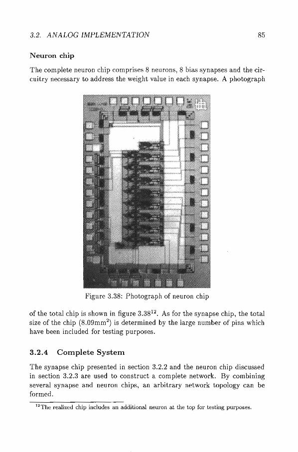
3.2. ANALOG IMPLEMENTATION 85
Neuron chip
The complete neuron chip comprises 8 neurons, 8 bias synapses and the circuitry necessary to address the weight value in each synapse. A photograph
Figure 3.38: Photograph of neuron chip
of the total chip is shown in figure 3.3812. As for the synapse chip, the total size of the chip (8.09mm2
) is determined by the large number of pins which have been included for testing purposes.
3.2.4 Complete System
The synapse chip presented in section 3.2.2 and the neuron chip discussed in section 3.2.3 are used to construct a complete network. By combining several synapse and neuron chips, an arbitrary network topology can be formed.
12 The realized chip includes an additional neuron at the top for testing purposes.

86 CHAPTER 3. IMPLEMENTATION
Here, an experimental setup contains 2 synapse chips and 2 neuron chips with which a two-layer network can be constructed with a maximum of 8 inputs. Each neuron chip contains 8 neurons and consequently the largest network topology which can be realized is a fully connected 8-8-8 network.
The setup is connected to a Sun SPARCstation 10 through a high-speed data acquisition board. Besides the 4 neural chips, the board contains multiplexing and de-multiplexing circuitry for (serial) communication with the data acquisition board, address selection, and several bias voltage and currents generators. Due to the experimental nature of the setup, separation of analog and digital signals on the board is far from ideal and cross-talk from the digital lines on the analog signals is present. However, by careful design of the timing of the board, a practical setup has been realized. Additional details about the setup can be found in appendix A.
On the host computer, a neural software environment, called ANANAS, is implemented. Any learning algorithm runs on the host computer while the feed-forward operations through the network can either be performed by the analog hardware or simulated in software. A description of ANANAS can be found in appendix B.
Conclusion
An overview of the characteristics of both synapse and neuron chips are given in table 3.5. Details about the synapse and neuron implementation are given separately. The figures describe the characteristics of a single synapse or neuron unless indicated otherwise in the last column.
Comparing the CPWM synapse implementation of section 3.1.6 and the time-continuous synapse presented in section 3.2.2, it can be concluded that both approaches have similar characteristics. A four-quadrant CPWM multiplier will occupy an area which is approximately equal to the two-transistor analog multiplier (also four-quadrant) while the linearity between input and output of the CPWM synapse is better (linearity between weight and output are similar in both cases) . The analog synapse consumes less power although an additional block per column of synapses is necessary. Propagation delay per layer of a network is in both cases in the order of lps. These findings comply with the comparison between CPWM and analog multipliers presented in section 3.1.5.

3.3. MODELING 87
I Property Value Remarks
Synapse Size 15,500fLm:l average size in a
column of 8 syn. Power consumption 2.25fLW Power consumption common load + OTA lOOJ.LW Input range [2V;3V] Weight range [OV;lV] Output range [-3J.LA;3J.LA] per column of syn.
independent of the nr. of active syn.
Input offset ~lOmV
Weight offset ~lOmV
Output offset ~o.SfLA per column of syn. Weight access time 250ns
Neuron Size 103,640fLm:l including bias weight Power consumption 700fLW including bias weight Min. input range [-0.5J.LA;0.5J.LA] Max. input range [-5f,lA;5fLA] Output range [2V;3V] Input offset O.l5fLA Bias weight range [OV;l V] Bias weight output current [-5J.LA;5fLA]
Layer Propagation delay ~ lfLS C1oad ~ lOpF
Table 3.5: Chip characteristics
3.3 Modeling
Recently, more and more complete neural network solutions are appearing. In most cases these packages consist of a dedicated NN chip, implementing some neural network structure at high speed, interface boards, connecting the chip to a controlling host (PC or workstation), and software.
In many cases, it is important to explore the features of a certain applic-

88 CHAPTER 3. IMPLEMENTATION
ation without having the whole package at once. In that case, the control software must be able to simulate the whole environment, including the NN chip. It is then necessary to have an accurate model of the chip inside a simulator.
Custom chips [OWH94, CR95], are fabricated containing building blocks (i.e. neurons, synapses) necessary to implement different neural network structures. In the ideal case, the building blocks behave in exactly the same way as their theoretical models. However, this is normally not the case; e.g. synapses do not produce a linear multiplication over the whole range. A model of each individual building block would be desirable as this could be used to predict the behaviour of larger networks constructed with these building blocks. A general model with several measurable parameters for each of the building blocks has been determined. The models can be used in neural simulators which have been written in recent years, e.g. ANANAS (see appendix B) and EL-SIM [CBP+95).
A heuristic model and characterization can be used to replace time consuming circuit simulations of large circuits with accurate models of circuit behaviour as a function of process parameters and working conditions (e.g. SPICE circuit simulator). Polynomial regression has been proposed [LD89) to approximate arbitrary and non-linear functions. Usually quadratic or third order models are used and they provide a fast and accurate relationship between random process parameters, physical parameters (i.e. temperature, power supply, frequency) and circuit performances.
3.3.1 Synapse Model
Ideally, synapses consist of linear multipliers between inputs Xi and weights Wij· Measurements on realized YLSI implementations (see figure 3.39(a)), show a different behaviour where inputs, weights and output are affected by offset and the multiplication is not linear. All these non-ideal effects also depend on working conditions such as temperature T, power supply Vdd,
frequency J, etc.
To obtain a computationally simple synapse model (both to determine its parameters and to use it in the simulators), non-idealities at the output of synapses are described as non-idealities in the inputs. The multiplication is then modeled with only offset and gain, while the two inputs are described with a third order polynomial function as presented in equation 3.27 where Xi represents the input and Wij the weight value, respectively. With this kind of model a compromise is found between different factors such as simplicity,

3.3. MODELING 89
computational time, and accuracy of the fit .
where each parameter aj, bj, Cj, dj is:
(3.28)
(3.29)
(3.30)
Figure 3.39(a) shows the comparison between measurements (points) 13 , and
·4L_~~~~~~~~~~
·1 ·0.8 ·0.6 ·0.4 ·0.2 0 0.2 0.4 0.6 0.8 1
(a) (b)
Figure 3.39: Different examples of synapse model/measurement comparison.
the model used (lines). The fitting is made using linear regression methods. The second plot, figure 3.39(b), shows the comparison between the model and an artificially modified set of measurements in the case highly non-linear effects are present in the multiplier characteristic.
Each parameter in 3.27 is a function of the most important working conditions (equations 3.28, 3.29, 3.30). The functions (F;, Gi, etc.) can be easily determined by changing only the correspondent working condition and repeating the fit process for the whole model. The values of the parameters at different working conditions are then used for another polynomial regression to find the desired functions. In figure 3.40 two example plots are shown.
13 Measurements are taken from the synapse chip presented in section 3.2.2.

90
0.7
0.65 ~ ............ .,... .. ___.-~
/ . 0.6 ;/
N u. 0.55 .,,~···
.. · 0.5 / .
0.45 ~-~
0.4 4.4 4.6 4.8 5 5.2 5.4
Power supply (volts)
3.3.2 Neuron Model
5.6
CHAPTER 3. IMPLEMENTATION
2.9
2.85
2.8
2 .75 N (!)
2.7
2 .65
2.6
2.55 4.4 4.6 4.8 5 5.2 5.4 5.6
Power supply (vohs)
With some neural VLSI implementations, it is possible to perform measurements on both synapse and neuron blocks separately [OWH94, Leh94], while other realizations only offer the possibility to examine the relationship between inputs and outputs of a complete layer (i.e. the combination of synapses and neurons) [CR95] .
Using the same technique as before, non-idealities at the out put of a neuron (and so of the non-linear function, e.g. a sigmoid) are modeled , as non-idealities in the inputs. The model used here (equation 3.31) is more complex than the one in the case of a synapse due to the presence of the neuron transfer function.
(3.31)
In the case of a model for a single neuron, Mj only depends on the input s1 of the neuron :
(3.32)
while in the case of a model for a complete input-output relationship (synapse +neuron), Mj depends on both synapse input Xi and weight value W ij:
(3 .33)
As with the synapse model, the parameters of the model are dependent on operating conditions:
(3.34)

3.3. MODELING 91
(3.35)
Here, a genetic algorithm approach [Gol89] is used in order to have a completely general solving method also in the case of a different non-linear function. Figure 3.41 shows two different cases of artificially generated neuron
1.2 .-~~~~~~-... ~"~ ..... ~ ••• -= ••• ~ .• ---:-:1,, ,. 0.8
... ~I
0.6 i ) 0.4
0.2
0
-0.2
ill ./
·0.4 ... /
-0.6 .......... .. -0.8 u:_:..__~~~~~-~~~...J
·1 ·0.8 -0.6 ·0.4 ·0.2 0 0.2 0.4 0.6 0.8 1
0 .6
0.4
0.2
0
-0.2
-0.4
I ·
;> ,. _,/.:·
-0.6 .............. ~ ... ·" -0.8 '--~~~~~~~-~_,____j
-1 ·0.8 -0.6 -0.4 -0.2 0 0.2 0.4 0.6 0.8 1
Figure 3.41: Different examples of 1/0 neuron transfer characteristic.
transfer functions (points) and the result of the model (line). Both characteristics contain extreme deviations (offset in both in put and output, a discontinuity around zero, noise on separate 'measurements') to test the robustness of the model. Even with these deviations present, the model of equation 3.31 is capable of producing a good fit.

92 CHAPTER 3. IMPLEMENTATION

Chapter 4
Learning
One of the main reasons for using analog electronics to realize neural network hardware is that several of the operations in neural networks can be realized by simple analog circuits, e.g. sigmoids, adders, simple multipliers. It is believed that the fault-tolerant nature of neural networks will compensate for the lack of accuracy in analog realizations. However, a distinction can be made between the realization of the feed-forward part of a network and the implementation of the learning algorithm. Several learning algorithms and their properties with regard to an analog implementation will be discussed.
4.1 Back-Propagation
Currently, one of the most used training algorithms is the back-propagation algorithm [RHW86] and in the last few years several hardware implementations of this algorithm have appeared , some digital [YMY+93, VM92] and some analog [FA88, SKK+92, LB93b, LB93a]. Others [HHP90, RF91, HH93, FH91] have reported on the problems which can occur when backpropagation is implemented and how these problems can be solved . However, most of these efforts have concentrated on the influence of finite precision constraints on the weights and other non-idealities which can be modeled as noise.
Back-propagation can learn to compensate for several non-idealities such as non-linear multipliers, limited signal dynamic ranges, and variability in multiplier gains [DC93]. In this section, the back-propagation algorithm will be studied further in combination with offsets in the multipliers necessary to implement the algorithm 1 using the CPWM-technique [P93]. Note that the
1 In parallel with this work, others [DC93, LB93a] have reported similar experiences .
93
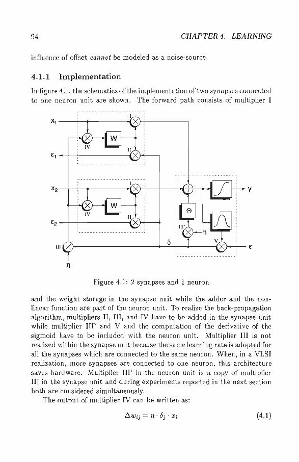
94 CHAPTER 4. LEARNING
influence of offset cannot be modeled as a noise-source.
4.1.1 Implementation
In figure 4.1, the schematics of the implementation of two synapses connected to one neuron unit are shown. The forward path consists of multiplier I
r- - - - - - - - - - - - - - - - - - - - - - - -1
' ' ' ~'---------,
: - - - - - - - - - - - - - - - - - - - - - - -: l----r---+--T---f y
Ill
Figure 4.1: 2 synapses and 1 neuron
and the weight storage in the synapse unit while the adder and the nonlinear function are part of the neuron unit. To realize the back-propagation algorithm, multipliers II, III, and IV have to be added in the synapse unit while multiplier III' and V and the computation of the derivative of the sigmoid have to be included with the neuron unit. Multiplier III is not realized within the synapse unit because the same learning rate is adopted for all the synapses which are connected to the same neuron. When, in a VLSI realization, more synapses are connected to one neuron, this architecture saves hardware. Multiplier III' in the neuron unit is a copy of multiplier III in the synapse unit and during experiments reported in the next section both are considered simultaneously.
The output of multiplier IV can be written as:
( 4.1)

4.1. BACK-PROPAGATION
with
where
TJ learning rate, Ej back-propagated error from next layer,
F; () derivative of the sigmoid, 8j error signal for all synapses connected,
to this neuron, Xi input of the synapse.
95
( 4.2)
The weight update given by equation 4.1 is exactly equal to the weight update as computed by the back-propagation algorithm (see equation 1.10).
4.1.2 Offset in forward path
In the forward path, several sources of offset can be identified i.e. offset at the output2 of multiplier I, offset in the adder of a neuron, and a horizontal shift in the position of the sigmoid. However, these errors can easily be compensated by the learning algorithm. They can be seen as a change in the bias weight of the sigmoid. Although care should be taken that the deviation in that parameter stays within reasonable bounds when more and more synapses are connected to the same neuron. Furthermore, an offset in the output of a neuron can be present, causing a vertical shift of the nonlinearity. The input range of synapses in the next layer should be sufficiently large to deal with this.
4.1.3 Offset in backward path
Offsets in the multipliers for the backward path cause more problems. In table 4.1, some simulation results are collected3 . The first five columns indicate the amount of offset which is introduced at the output of each multiplier. It is given as a percentage of the output range e.g. if a multiplier can output values between -2.5 and 2.5, an offset of 1% will add a constant value of 0.05
2 0ffset at the input could also be considered but will not be explicitly studied here because in most cases offset at the input of a multiplier can be modeled as offset at the output of a preceding block.
3 During simulations, the only non-idealities introduced were the offsets in the multipliers and restrictions on the range of the weights from -2.5 to 2.5 and the output of multiplier V from -1.0 to 1.0. Other non-idealities, like quantization of weights, non-linearities, etc. were not considered here.

96 CHAPTER 4. LEARNING
to the output. In column 6, the number of converged trials (out of 100) of teaching a 2-2-1 network the XOR-problem is shown.
offset in multiplier converged trials I J II I III I IV I v out of 100
0 0 0 0 0 67 0 1 0 0 0 67 0 2 0 0 0 18 0 0 1 0 0 85 0 0 2 0 0 48 0 0 0 1 0 70 0 0 0 2 0 67 0 0 0 0 0.5 73 0 0 0 0 1 86 0 1 1 1 0.5 9 0 2 2 2 1 0
Table 4.1: Influence of static offsets
In the case of a small offset (separately introduced) in multipliers III and V convergence rates increase significantly4 • Both effects can be explained by the fact that paralysis of the network during learning is avoided when a neuron output is saturated. A zero-valued output of the sigmoid derivative would normally 'block' the back-propagation of the error c. By making sure that at least some value is propagated back through the network, weight updating continues5 . Offset introduced in multiplier II has a large influence on the convergence property of the network. A change of sign in the signal which is being back-propagated (8 in figure 4.1) is severe.
When each offset is introduced separately, convergence of the network is still possible. However, when all offsets are applied simultaneously, the effects are catastrophic; even small amounts of offset result in no convergence at all. During the simulations, all introduced offsets had the same sign resulting in a worst-case situation. The introduced offset for multiplier V is kept low because in the proposed implementation [P93] this multiplier is
4 Assuming convergence of the network is based on a binomial distribution , for 100 trials, the maximum standard deviation is 5 (for P convergence = 0.5) .
5 ln [Fah88] a heuristic approach to improve convergence of the back-propagation algorithm is proposed which is similar to the effect observed here.
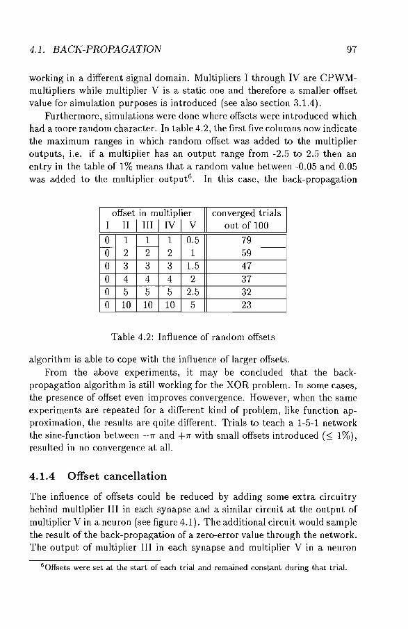
4.1. BACK-PROPAGATION 97
working in a different signal domain. Multipliers I through IV are CPWMmultipliers while multiplier V is a static one and therefore a smaller offset value for simulation purposes is introduced (see also section 3.1.4).
Furthermore, simulations were done where offsets were introduced which had a more random character. In table 4.2, the first five columns now indicate the maximum ranges in which random offset was added to the multiplier outputs, i.e. if a multiplier has an output range from -2.5 to 2.5 then an entry in the table of 1% means that a random value between -0.05 and 0.05 was added to the multiplier output6 . In this case, the back-propagation
offset in multiplier converged trials
I I II I III I IV I v out of 100
0 1 1 1 0.5 79 0 2 2 2 1 59 0 3 3 3 1.5 47 0 4 4 4 2 37 0 5 5 5 2.5 32 0 10 10 10 5 23
Table 4.2: Influence of random offsets
algorithm is able to cope with the influence of larger offsets. From the above experiments, it may be concluded that the back
propagation algorithm is still working for the XOR problem. In some cases, the presence of offset even improves convergence. However, when the same experiments are repeated for a different kind of problem, like function approximation, the results are quite different. Trials to teach a 1-5-1 network the sine-function between -rr and +rr with small offsets introduced (s; 1%), resulted in no convergence at all.
4.1.4 Offset cancellation
The influence of offsets could be reduced by adding some extra circuitry behind multiplier III in each synapse and a similar circuit at the output of multiplier V in a neuron (see figure 4.1). The additional circuit would sample the result of the back-propagation of a zero-error value through the network. The output of multiplier III in each synapse and multiplier V in a neuron
6 0ffsets were set at the start of each trial and remained constant during that trial.

98 CHAPTER 4. LEARNING
would indicate the error in the weight updated due to offsets in the backpropagation path. When these values are stored and later subtracted from the 'normal' weight update, the offset contributions will be eliminated. The extra circuitry will also introduce some errors but these will be of secondorder influence. A similar approach has been reported in [MA94].
The speed of the back-propagation algorithm is influenced. The backpropagation of a zero-error has to be performed before every 'real' backpropagation pass, as the offsets are dependent on the current state of the network, i.e. the output values of neurons and the weight values. It should be clear that the state is different for each input vector and after each update of the weights.
During simulations, the earlier mentioned second order effects of the extra circuitry were neglected. In that case, the network with offsets, extra circuitry, and the back-propagation of a zero-error before every 'real' backpropagation pass behaves just like an ideal network without offsets. Then, for the XOR-problem roughly two-third of the trials converged (which corresponds to the case when no offsets were introduced, see table 4.1) and the sine-function could now also be learned without any problem.
4.1.5 Conclusion
The analog implementation of back-propagation suffers heavily from the influence of offsets which are present in the multipliers in the back-propagation path. The offset problem can be reduced by adding extra circuitry which performs some kind of auto-offset cancelling. However, this is at the expense of the speed of the back-propagation algorithm.
Furthermore, the amount of hardware necessary to implement the backpropagation algorithm is large (see figure 4.1). When the algorithm is being implemented as part of a system which should be able to adapt to its environment over time, special attention should be paid to the back-propagation algorithm itself before implementing it. The major drawback of the algorithm in such an environment is that incremental learning is very difficult with the back-propagation algorithm. Usually, all previous training data has to be available which results in large storage requirements and long convergence times. Enhancements of the algorithm as proposed in section 1.2.4 could be used to speed up learning. However, hardware implementation of these enhancements would further complicate the design.
In commercial applications, hardware neural network implementations including learning circuitry to realize the back-propagation algorithm might not prove to be cost effective. The large extra implementation area for the

4.2. SEMI-PARALLEL PERTURBATION 99
learning, in most cases, will only be used once. After the desired functionality has been achieved, weights are frozen7 and, for the life-time of the product, learning is not continued or repeated. In those cases, a global learning engine, possibly enhanced with a small amount of extra circuitry at a local level, which trains the desired functionality will be advantageous.
Here, several feed-forward based learning algorithms will be discussed. Analog hardware implementations of the feed-forward path are used while learning is performed by a host computer or dedicated digital hardware.
4.2 Semi-parallel perturbation
The original Weight Perturbation algorithm (see section 1.2.5) is sequential. Each weight is perturbed and, depending on the update strategy, updated separately. Especially for large networks, this can be a slow process. Several semi-parallel8 perturbation-based learning schemes have been proposed:
• With the Summed Weight Neuron Perturbation (SWNP) algorithm [FJ93], all the weights feeding into one neuron are perturbed in parallel. Compared to the original WP algorithm, complexity is reduced by 0( VW") where W is the number of weights in a network. In [F J93], proof is given that for SWNP the descent steps in the direction of the negative of the gradient are larger in size than the steps in the wrong direction, and hence SWNP performs error descent. The SWNP learning rule iterates over all the neurons. The learning rule for neuron j is:
,6.wiJ = -ry E(W')- E(W) OWij
( 4.3)
where W is the matrix of all weights in a network, W' is the matrix of weights where the weights feeding into neuron j are perturbed, and OWij is the perturbation size for weight Wij.
• In contrast with SWNP, in the fan-out technique [JCF96] all the weights leaving a neuron are perturbed simultaneously using uncorrelated random values. Experiments in [JCF96] show that the fan-out algorithm provides a significant improvement in training performance compared to WP and SWNP.
7 Depending on the way weight storage is implemented, this might be done in e.g. a floating-gate memory or a digital memory with periodic refresh .
8 More than one weight but less than the total number of weights in a network are perturbed simultaneously.

100 CHAPTER 4. LEARNING
• A combination of the above perturbation schemes results in the fan-inout technique [JCF96]; all the weights feeding and leaving a neuron are simultaneously perturbed using uncorrelated random values. The learning rule is equal to 4.3 where in matrix w' only the weights feeding and leaving a neuron are perturbed. From the experiments reported in [JCF96) it is concluded that the fan-in-out scheme consistently produces the best performance.
In the experiments performed here, only the fan-in-out technique will be used as semi-parallel perturbation technique.
The fan-in-out algorithm as described in [JCF96] cannot be directly used in combination with the hardware developed here (see section 3.2.4). The main difference is that the analog neural network implementation presented in [JCF96) does not include a bias weight in each neuron. When training a 2-layer network in that implementation, only the neurons in the hidden layer have to be 'visited' by the fan-in-out algorithm. In that way, all weights in the network are updated. However, here, with that strategy, the bias weight of the output neuron would not be updated. Therefore, here, the fan-in-out algorithm will 'visit' all neurons in the network (both hidden and output neurons) but in addition also the input nodes. Although the input nodes are no real neurons, the reason for also applying the fan-in-out algorithm is that in that way all weights in the network9 are updated an equal number of times, namely 2, per epoch.
As noted in section 1.2.5, the error which is made when estimating the gradient with respect to a weight, can be reduced by performing two opposite perturbations per gradient estimation (Central Difference Method, CDM). In relation to an analog hardware implementation, the CDM method is advantageous as a larger perturbation size can be used to obtain the same performance (convergence rate and final error) [tK93]. The learning rule for the fan-in-out algorithm with double sided perturbation can be expressed as:
E(W') - E(W") flWij = -7]
2_. UWij
( 4.4)
w' denotes the weight matrix where all weights feeding and leaving a neuron are perturbed simultaneously with their respective perturbation 8Wij, while w" denotes the weight matrix where the same weights are perturbed with -8Wij. In the experiments reported later, the size of the perturbation is fixed while the sign of each perturbation is chosen randomly.
9 With the exception of the bias weights.

4.3. FULLY PARALLEL PERTURBATION 101
Both pattern- and set-based update strategies are used in conjunction with the fan-in-out algorithm. In section 4.6, both versions are compared to the other algorithms presented here.
Two different hardware implementations of the fan-in-out algorithm can be considered:
• A global computation core, e.g. a Digital Signal Processor (DSP), sequentially visits each neuron, perturbs the weights (one or more times) and determines the weight updates. In such a case, weights can best be stored in a digital form as perturbations have to be applied and removed. Furthermore, a minimum amount of extra hardware per synapse is necessary. A large degree of flexibility is obtained in this way.
• A distributed approach in which extra circuitry is added per synapse. A small global control unit indicates which synapses should perturb their weights (one or more times). After an error evaluation has been performed, each synapse locally computes an update value and applies it to the current weight value. A drawback of this approach is that for long-term storage of the weights (after learning has converged), it should be possible to read out weight values. Additional hardware has to be added for this as well .
4.3 Fully parallel perturbation
Recently, fully parallel perturbation schemes have been reported (Cau94, Cau93, AMY+93] . The learning rule for these algorithms is equal to the one presented in the previous section (equation 4.3). However, in this case all weights in the network are perturbed simultaneously. As for the semiparallel algorithms, a double sided perturbation (equation 4.4) yields a more accurate result.
In an analog environment, the minimum perturbation size is determined by the noise-level in the total system. When the perturbation size is chosen in the same order of magnitude as the noise in the system, the correlation between the applied perturbations and the measured difference in error will be small and learning is slowed down and possibly prevented. In practice, the fully parallel algorithms are used with a perturbation which is constant in magnitude but has a randomly generated sign; also called Constant Perturbation Random Sign (CPRS). The minimum perturbation size is determined experimentally.
102 CHAPTER 4. LEARNING
CPRS essentially performs gradient descent in random direct ions in the weight space. As for exact gradient descent (e.g. the sequential WP algorithm) the parallel algorithm converges in close proximity of a (local) minimum, provided that the perturbation amplitude is sufficiently small10.
The speed of convergence is necessarily slower than gradient descent, since every computation of the total errorE only reveals scalar information about the gradient. The accuracy at every learning step can be improved by repeating the parallel perturbation many times before updating the weights. In [AMY+93], a critical minimum of repeating each perturbation step 16 times is reported. Especially in larger networks, it might prove necessary to repeat each perturbation step a large number of times, thereby reducing the advantage of less perturbation steps over semi-parallel algorithms.
Experiments (see section 4.6) have shown that a pattern-based update strategy does not work very well with the parallel perturbation technique. The reason for that is that the weights are updated based on the presentation of a single pattern. The resulting PMSE does not reveal sufficient information about the gradient in the total error space (determined by all training patterns).
Considerations for a hardware implementation of CPRS are similar to the ones mentioned in the previous section. A distributed analog implementation of CPRS is presented in [Cau96].
4.4 Alopex
In the original Alopex algorithm, as described in section 1.2.6, both global and local information is used during training. Globally, the error E (t), the change in error b.E(t), and the temperature T(t) are determined . For each weight, hence locally, the change in the weight value b.Wij(t), the correlation between the change in error and the weight change b.ij(t), and the probability Pij(t) for choosing the sign of the weight update need to be computed and/or stored.
When the algorithm needs to be implemented on dedicated digital hardware or on a host computer, reducing the number of items which need to be computed for each synapse separately saves complexity. A global 'flipprobability' PJ(t) is introduced: the probability that the sign of the update of a weight, with respect to the previous update, needs to be changed . P1(t)
10 A formal derivation of the convergence properties is presented in [Cau93].
4.4. ALOPEX 103
is defined as: 1
P1 ( t) = _1_+_e ___ 1J Ll-:-E=(;-;t )"7./T=(""7t) (4.5)
where 7J is the learning rate and the global temperature T(t) is the average over a number of error changes, respectively. In the originaJ algorithm [UV92] the temperature was determined by storing a number of error changes and averaging them at each time step. Here, a moving average for the temperature will be used, further reducing the storage requirements:
T(t) = 0.1I~E(t) I+ 0.9T(t- 1) (4.6)
The only information which needs to be computed and stored locally is:
() ( 1) { -~Wij(t) with prob. PJ(t)
Wi · t = Wi · t - + J J +~Wij(t) with prob. 1- P1(t)
(4.7)
Effectively, this results in an algorithm which behaves in the same way as the original Alopex algorithm, but with significantly less local information to be stored and computed. The complete algorithm can now be described as:
1. (a) Select initial random weight vector w(t = 0) and a starting temperature T(t = 0).
(b) Compute the system error E(t = 0) for the initial weight values.
(c) Generate a random binary update vector .Q(t = 0) with elements bi. The elements can either be + 1 (increase weight) or -1 (decrease weight).
(d) Choose a step-size 8 and a learning rate 7J (usually in the order of 1.0).
2. (a) Update the weights according to: w(t) = w(t- 1) + 8 · .Q(t- 1) resulting in a new value for the error E(t).
(b) If E(t) < c (c being the convergence limit on E), stop.
3. (a) Compute the change in error: ~E(t) = E(t)- E(t- 1).
(b) Update the temperature as described in equation 4.6.
(c) Determine the new global flip-probability PJ(t) (equation 4.5).
(d) Update the binary update vector .Q(t):
b·(t) = { - bi(t- 1) with prob. PJ(t) 1 +bi(t- 1) with prob. 1- PJ(t)

104 CHAPTER 4. LEARNING
(e) Go to step 2.
Extensive simulations [Vog95) have shown that the influence on the convergence behaviour of both the learning rate ry and the way temperature T(t) is determined are small. The number of converged runs can be significantly increased by choosing a small step-size fl, however, at the cost of an increased number of epochs to reach a solution. As for the other feed-forward based learning algorithms introduced here, the minimum step-size is determined by the noise-level in the system.
Note that Alopex does not perform gradient descent. Weights are perturbed and depending on the change in error, the probability that during the next perturbation step, the direction of perturbation remains equal is determined. The algorithm has a preference to follow a trajectory opposite to the gradient but due to the stochastic nature it offers the possibility to escape from local minima.
A major advantage with regard to the earlier presented feed-forward based learning algorithms is the fact that perturbations do not have to be removed. This is especially important in the case of a complete hardware implementation of the algorithm . Again, a choice could be made between a global and a distributed implementation. In the former case, no additional circuitry per synapse is required while in the latter case, a simple single-bit memory element per synapse could indicate the direction of the last weight update. At a global level, an error evaluation should be done in both cases. The flip-probability for each weight could also best be determined globally as an implementation on synapse level would require a significant amount of additional circuitry.
As for the parallel perturbation algorithm, a pattern-based update strategy should not be used in conjunction with Alopex. The information contained in one feed-forward operation does not reveal sufficient knowledge about the total error landscape. Then, the stochastic property of the algorithm is more of a burden than a solution to escape out of local minima.
4.5 Probabilistic Optimization
Currently, very little is known about the shape of error landscapes. Gradient descent and approximate gradient descent (e.g. the parallel perturbation algorithm) methods are mostly used to find a solution in the high-dimensional solution space. However, numerous experiments in the literature have shown that these algorithms often get stuck in a local minimum. Several heuristic solutions to escape from these minima have been proposed.
4.6. LEARNING EXPERIMENTS 105
Purely probabilistic methods to train neural networks are also still popular. These methods do not make any assumptions about the shape of the error landscape and try to find an acceptable solution by searching the solution based on a stochastic process (in most cases combined with several heuristic modifications).
In section 1.2.6, several stochastic learning algorithms have been introduced. Here, an adapted version of MROM will be used to train a network. The used algorithm consists of the following steps:
1. Select an initial random weight vector w(t = 0) and a range for the uniform distribution.
2. Generate a random vector ~(t) of which each element is taken from this uniform distribution:
(a) If E(w(t) + ~(t)) < E(w(t)), then let w(t + 1) = w(t) + ~(t) (b) If E(w(t) +~(t)) ~ E(w(t)) and E(w(t)- ~(t)) < E(w(t)), then
let w(t + 1) = w(t)- ~(t)
(c) Otherwise, let w(t + 1) = w(t).
3. If E(w(t)) < E, stop. Otherwise, go to step 2.
The major difference compared to the original MROM algorithm is that { is not taken from a Gaussian but from a uniform distribution. Experiments in which the above algorithm was used to train the analog neural hardware revealed that convergence properties (for several different problems) in the case of a Gaussian distribution were much worse than for a uniform distribution. While a Gaussian distribution yields a random vector {in which the elements could have a large value, thereby offering the possibility to escape from local minima, the majority of the generated values are small. Therefore, most of the generated values are in the same order of magnitude as noise in the system and learning is slowed down.
As perturbations are chosen from a range of values and have to be applied and possibly removed (when no improvement in error is observed), a global hardware implementation with digital storage of weights would be the most appropriate with MROM.
4.6 Learning Experiments
The complete system, described section 3.2.4 and appendix A, has been used to perform several learning experiments. Feed-forward operations are

106 CHAPTER 4. LEARNING
performed by the analog hardware while the learning algorithm runs on the host computer in the ANANAS software environment.
In software simulations, all learning algorithms used here perform best when the perturbation size is chosen very small. However, in conjunction with analog neural hardware, the smallest perturbation is the perturbation that provides the algorithm with sufficient information to perform error descent in the weight space. When perturbations are chosen too small, the resulting effect (e.g. in the change in error criterion) is lost in the noise in the system. In the experiments reported here, for each algorithm, the minimum perturbation size was determined experimentally (see appendix C). Choices for other parameters are based on several pre-runs per algorithm and problem, and are chosen in such a way that no oscillations are observed in the TMSE.
Weights in both synapse and neuron chips were refreshed prior to each feed-forward operation. One feed-forward operation through the network, including communication between the host computer and the analog hardware, and propagation delay through the (analog) chips, amounts to 40J.Ls (see appendix A for additional details).
4.6.1 Epochs
An epoch is defined as an update of all the weights in a network using all the patterns in the training set. Depending on the algorithm the number of feed-forward operations through the network to perform one epoch differs. Table 4.3 shows the number of feed-forwards for each of the algorithms
Algorithm
fan-in-out CPRS Alopex MROM
# Feed-forwards per epoch 2 X (N +I) X P 2 X P p
~~xP
Table 4.3: Number of feed-forwards per epoch for each training algorithm where P is the number of training patterns, N the number of neurons in the network and I the number of inputs of the network. Note that in a 4-8-3 network, there are 11 neurons (8+3) and 4 inputs.
used here. For both the fan-in-out and the CPRS algorithm, the Central

4.6. LEARNING EXPERIMENTS 107
Difference Method is used to determine weight updates. In the case of the fan-in-out algorithm, during one epoch all weights (with the exception of the bias weights) are updated twice. Hopefully, this will result in a reduced number of epochs necessary to reach convergence. The number of feed-forwards for the probabilistic algorithm, MROM, is approximated as either one or two feed-forwards are done each algorithm step (see part 2 of the algorithm in section 4.5).
Three problems have been studied, parity-4, parity-5, and a function approximation.
4.6.2 Parity-4
For parity-4, the task is to determine the parity of a binary 4-dimensional input vector. There are 16 training patterns. In all cases, a 4-6-1 network was used and the learning is considered to have converged when a TMSE of 0.01 has been reached. A logical '0' in both input and target patterns is represented by a value of -0.9 and a logical '1' by 0.911 . At a TMSE of 0.01, on average the output of the network has reached the target value within a range of 0.1. Although, learning could be said to have converged when a decision threshold between '0'- and '1 '-levels can be determined, a larger noise margin is established when learning is continued. Especially in the presence of leaking weights (see section 4.7), this is advantageous.
Algorithm Epochs # ff's Converged Average Std. Dev. Average
fan-in-out pattern 1,312 473 461,824 56%* fan-in-out set 3,228 698 1,136,256 88% CPRS pattern 5,830 2,418 186,560 40% CPRS set 7,007 2,175 224,224 55% Alopex 12,718 6,885 203,488 81% MROM 4,483 1,440 107,592 63%
Table 4.4: Summary of teaching a 4-6-1 network the parity-4 problem; 100 runs(*: 25 runs).
11 The value is dimensionless as it is the value which is used within the software. The voltage output of the neuron (between 2V and 3V) is transformed to the dimensionless range from -1 to +1.

108 CHAPTER 4. LEARNING
Table 4.4 summarizes the training results, showing the average and standard deviation of the number of epochs to converge, the average number of feed-forwards, and the percentage of runs which converged (out of 100 runs), respectively. The first three numbers are computed over the runs which converged. Detailed information about the different parameters in each algorithm can be found in appendix C.
While the largest number of runs converges using the fan-in-out algorithm with a set-based update strategy, it also needs the largest number of feed-forwards to achieve this performance. CPRS with a pattern-based update clearly performs worse than all others. Alopex combines a low number of feed-forwards with a high convergence rate. Surprisingly, the algorithm which makes the least assumptions about the shape of the high-dimensional error landscape, MROM, needs the lowest number of feed-forward operations and converges in about 2/3 of the cases.
Software simulations in which only a restricted weight range of [ -5.0; 5.0] and a simplified model of a synapse and neuron 12 were used, confirm the above behaviour. The simulations resulted in comparable convergence rates and speed.
4.6.3 Parity-5
In the case of parity-5, a 5-dimensional binary input vector has to be classified depending on even or odd parity. In total, 32 input-output combinations are used during training of a 5-8-1 network. As for the parity-4 problem, learning has converged when a TMSE of 0.01 is reached.
Table 4.5 shows the results which are very similar to the case of the parity-4 problem. The fan-in-out algorithm with a set-based update strategy still converges in the largest number of runs at the cost of a very large number of feed-forwards. Again, MROM converged in about 2/3 of the cases in the least number of feed-forwards.
4.6.4 Function Approximation
Historically [MP69], parity problems have been popular to test the ability of neural networks for solving highly non-linear problems. However, one of the powerful features of a neural network, its generalization performance, cannot be tested/measured with such a problem. Generalization can be
12 In the simplified model only the gain of the hardware system was modeled. In that way, the influence of a restricted weight range is similar in both hardware runs and software simulations.

4.6. LEARNING EXPERIMENTS 109
Algorithm Epochs # ff's Converged Average Std. Dev. Average
fan-in-out pattern 1,364 844 1,222,144 56%* fan-in-out set 5,961 1,503 5,341,056 94% CPRS pattern 11,494 6,332 735,616 8%* CPRS set 14,170 4,130 906,880 50% Alopex 23,966 8,202 766,912 57% MROM 8,898 3,459 427,104 64%
Table 4.5: Summary of training a 5-8-1 network the parity-5 problem; 100 runs (*: 25 runs).
defined as the ability of a network to produce a meaningful response to an input which has never been presented to the network before. In most real-world applications, a response which is similar to an input the network did see during training produces satisfactory generalization. In the case of a parity problem, a minimum change in the input (flipping one bit in the input word), should result in a maximum change in the output of the network (from a logical '0' to a logical '1 ').
Here, the generalization property of the network is tested by trying to learn a 1-5-1 network to produce the sine function. The training set consists of37 equidistant samples taken from y = 0.4·sin(7r·x), where -1 s x s +1. Learning is considered to have converged when a TMSE of 5e-4 has been reached 13 .
From the results in table 4.6, it can be seen that both versions of the fanin-out algorithm perform very well with respect to the number of converged runs, again at the cost of a large number of feed-forwards. CPRS with pattern-based update did not converge in a single run while Alopex also had problems to convergence. The step-size for Alopex had to be reduced to 0.01 (on a total range of 10) which effectively resulted in a random search as such a small step-size is almost indistinguishable from noise in the system. MROM combines the least number of feed-forwards with a high convergence rate.
Figure 4.2 on the left shows both the original sine-function and the output of the network for 200 input values between -1 and +1. The network output contains a significant amount of noise (approx. 5m Von a total output range
13 20 times smaller than in case of the parity problems!

110 CHAPTER 4. LEARNING
Algorithm Epochs # ff's Converged Average Std. Dev. Average
fan-in-out pattern 1,028 403 532,504 91% fan-in-out set 4,695 1,675 2,432,010 91% CPRS pattern - - - 0% CPRS set 20,225 4,705 1,496,650 84% Alopex 31,635 5,458 1,170,495 47% MROM 4,048 1,657 224,664 91%
Table 4.6: Summary of training a 1-5-1 network the sine function; 100 runs.
0.4 0.4
/ / " ' 0.3 // 0.3 I I
0.2 I
0.2 ,i I
I 0.1 I 0.1 I
l I ~ 0
.0.1
!J -0.1
-0.2
-0.3 ;} -0.3
/· .0.4 -0.4
·I .0.8 -0.6 -0.4 ·0.2 0 0.2 0.4 0.6 0~ I 0 02 0.4 0.6 o.e I Input l"pul
Single run Average over 5 runs
Figure 4.2: Sine-function approximation
of 1 V) which can largely be accounted to the experimental setup of the whole system (as described in appendix A). On the right, an average over 5 runs can be seen, showing that the network is very well capable of producing an acceptable output to an input it has never seen before.
4.6.5 Conclusion
The feed-forward based learning algorithm which needs the least effort to train an analog neural hardware implementation several functionalities, is a probabilistic algorithm (MROM) which makes very little assumptions on shape of the error landscape corresponding to the problem. The algorithm which implements a gradient descent algorithm (fan-in-out with a set-based update strategy) performs very well with respect to the number of runs which converge, hence it avoids and/or escapes from local minima.
The minimum perturbation size for an algorithm defines an effective

4. 7. WEIGHT LEAKAGE 111
weight accuracy for the totaJ system . For most of the algorithms here, a fixed perturbation size 8 of 0.05 on a total weight range of 10 works very well, corresponding to a weight accuracy between 7 and 8 bit. In the case of CPRS an even smaller perturbation size (8 = 0.025) had to be used (larger values resulted in unstable behaviour of the algorithm) although this caused CPRS to converge less frequently.
4. 7 Weight Leakage
Weights in the realized system are stored using a volatile method, by storing an amount of charge on a (small) capacitor (see section 2.5). During learning, the weights are refreshed from a digital memory before each feedforward operation. Then, the influence of leakage of the weights is minimal as each feed-forward operation only takes about 40J1s. However, after learning (in the case of a more practical application than the test-problems in the previous section), weights should be refreshed regularly to make sure the network keeps performing well on the learned classification or function approximation.
0.2
·0.2
-0.4
-0.6
·I OL_.....:::0:10==,.==30-~40==,.~~ .. Tim• in sec.
Solution 1 Solution 2
Figure 4.3: Influence of weight leakage on parity-3 problem
In figure 4.3, the output of a 3-4-1 network, which learned the parity-3 problem, versus time is shown. After learning converged, the weights were no longer refreshed and the output of the network for all 8 input patterns was determined each second. The two plots show the behaviour of the network for two different solutions (separate trials starting with a different set of initial weight values) of the network to the parity-3 problem. In the right plot, even after 60 seconds without any refresh, a distinction between a logical '0' and '1' can be easily made by applying a binary threshold around zero, while in the left plot, errors are made much earlier.

112 CHAPTER 4. LEARNING
0.6
o.•
! 0.2
·0.2
Solution 1 Solution 2
Figure 4.4: Influence of weight leakage on sine function approximation
A similar experiment was performed with a 1-5-1 network which learned to approximate the sine function. Figure 4.4 shows the input-output relation of the network at different time-steps after refreshing was stopped. Again, the two different solutions show very different behaviour to weight leakage. In contrast to the parity-3 problem, here the functionality of the network is already severely distorted after a few seconds.
Clearly, the influence of weight leakage is both problem and solution dependent. The refreshing frequency should therefore be chosen conservatively, e.g. 25Hz, which is still several orders of magnitude slower than the speed with which input vectors can be presented to the network, namely at 25,000 Hz. Such a refresh speed should not hamper the functionality of the network in most applications.
Research on practical applications [vSNS90] has shown that the faulttolerance of a neural network also depends on the used learning strategy. The influence of weight leakage could possibly be reduced by choosing the appropriate learning strategy; e.g. continuing learning for a certain time even when the error on the training set no longer decreases.
4.8 Conclusion
From a point of view of flexibility, a global, digital implementation of learning algorithms has preference. Furthermore, the lack of accuracy in analog learning algorithm implementations (e.g. back-propagation) causes learning to be difficult and slow. In addition, in commercial applications the large amount of extra hardware necessary to implement a learning algorithm in an analog, distributed way may not be cost effective.
A global, digital learning approach can best be combined with digital

4.8. CONCLUSION 113
storage of weight values and a periodic refresh to the analog feed-forward implementation of a neural network. The refresh rate can be much lower than the rate at which input vectors can be presented to the network.
A probabilistic algorithm (MROM) performs best with respect to the speed (number of necessary feed-forwards) at which solutions are found while Alopex is preferable with respect to the implementation complexity.

114 CHAPTER 4. LEARNING
Chapter 5
Concluding Remarks
The study described in this thesis has shown that simple, small, non-ideal, analog electronic building blocks can be used to construct neural networks. The complete realized system is one of the first systems reported with which real-time learning experiments have been performed. The following development stages have been passed through: 1) the initial idea to use simple building blocks, 2) the design and realization of a complete system, and 3) the choice of an appropriate learning algorithm and real-time learning experiments.
System
Maximum flexibility in the selection of network topology can be achieved by implementing synapses (in an array structure) and neurons (in a column structure) on separate chips (section 2.1). This flexibility introduces the need for scaling of electrical quantities in a network. Through a statistical analysis (under certain conditions), it has been shown that when the number of inputs to a neuron increases by a factor F, all weights to that neuron should be multiplied by a factor n (section 2.2).
Implementation
Two implementation approaches have been considered and compared; a time-sampled, pulse stream implementation where analog values are encoded using binary signals and an analog, time-continuous implementation.
• In the case of Coherent Pulse Width Modulation (CPWM), a compact, low-power two-quadrant multiplier has been realized in a 2.4JLm
115

116 CHAPTER 5. CONCLUDING REMARKS
CMOS process. For pulse-frequencies up to 1 MHz the measured multiplier characteristics show excellent linearity. The two-quadrant multiplier can easily be expanded to a four-quadrant one with similar characteristics (section 3.1.6).
• A complete, analog, time-continuous neural network implementation has been realized in a 2.4J.Lm process. The main building block, the synapse, consists of only 2 transistors and shows a linear behaviour at a low power consumption. The complete system consists of 2 synapse and 2 neuron chips capable of realizing an 8-8-8 network (section 3.2).
A comparison between the two computation schemes shows that they have comparable performance for low power consumption values. Bandwidth is slightly in favor of analog, time-continuous systems, while linearity is slightly in favor of CPWM systems (section 3.1.4).
To be able to simulate the behaviour of neural hardware realizations in a software environment, a general model for both synapse and neuron building blocks has been derived. In the case of a synapse, a third-order polynomial function has proven to be capable of fitting to highly non-linear multiplier characteristics. A model for a neuron consists of an exponential function combined with a third-order polynomial. The model is independent of the type of implementation and the model parameters can be determined easily and fast (section 3.3).
Learning
Analog on-chip implementation of the well-known back-propagation learning algorithm is not recommendable. It suffers heavily from the influence of offsets present in the multipliers needed to implement the algorithm. Furthermore, the large amount of extra hardware necessary to implement the back-propagation algorithm might not prove to be cost effective (section 4.1).
Several feed-forward based learning algorithms have been considered. Based on a number of experiments with perturbation-based and probabilistic algorithms in conjunction with the realized hardware, it can be concluded that a global, off-chip, digital implementation of a learning algorithm has preference. A probabilistic algorithm (MROM) performs best with respect to the speed at which solutions are found, while the Alopex algorithm is preferable with respect to the implementation complexity.
A global, digital learning approach can best be combined with digital storage of weight values and a periodic refresh to the analog feed-forward

117
implementation of a neural network. In the network , small capacitors within each synapse are used to store the weight values. The effective weight accuracy of the realized system lies between 7 and 8 bit.
Publications
The research for this thesis resulted in the following publications: [GW93, RWHC94, OWH94, Wit94b, vKCWH94, Wit95, WH95, Wit94a]

118 CHAPTER 5. CONCLUDING REMARKS

Bibliography
[AH87]
[APS95]
[Bab89]
[Bru93]
[Bru96]
[Cau93]
[Cau94]
P.E. Allen and D.R. Holberg. CMOS Analog Circuit Design. Holt, Rinehart and Winston, Inc., 1987.
J. Alspector, R. Meir, B. Yuhas, A. Jayakumar, and D. Lippe. A Parallel Gradient Descent Method fo r Learning in Analog VLSI Neural Networks, volume 5 of Advances in Neural Information Processing Systems, pages 836- 844. Morgan Kaufman Publishers, 1993.
C. Alippi , V. Piuri , and M. Sami. Sensitivity to errors in artificial neural networks: A behavioral approach. IEEE Transactions on Circuits and Systems-!, 42(6):358- 361 , June 1995.
N. Baba. A new approach for finding the globa l minimum of error function of neural networks. Neural Networks, 2:367-373, 1989.
P.P.F.M. Bruin. A weight perturbation neural net chip set. Master's thes is , Eindhoven University of Technology, August 1993.
P.P.F.M . Bruin. Electronics for cellular neural networks. Technical report , Stan Ackermans Institute, Eindhoven U niversity of Technology, May 1996.
G. Cauwenberghs. A Fast Stochastic Error-Descent Algorithm for Supervised Learning and Optimization, volume 5 of Advances in N eural Information Processing Systems, pages 244-251. Morgan Kaufman P ublishers, 1993.
G. Cauwenberghs. A Learning Analog Neural Network Chip with Continuous-Time Recurrent Dynamics, volume 6 of
119

120
[Cau96]
[CBS93]
[CM93]
[Cor95]
[CR95]
(CV93]
[DC93]
[DEDT96]
BIBLIOGRAPHY
Advances in Neural Information Processing Systems, pages 858-865. Morgan Kaufman Publishers, 1994.
G. Cauwenberghs. Analog VLSI stochastic perturbative learning architectures. Journal of Analog Integrated Circuits and Signal Processing, 1996. submitted.
M. Chiaberge, G. Di Bene, S. Di Pascali, R. Lambert, B. Lazzerini, A. Maggiore, and L.M. Reyneri. EL-SIM: a development environment for neuro-fuzzy intelligent controllers. In Proceedings IWANN95, June 1995.
J. Choi, S.H. Bang, and B.J. Sheu . A programmable analog VLSI neural network processor for communication receivers. IEEE Transactions on Neural Networks, 4(3):484-494, May 1993.
Y. Cao and S. Mattisson. Current-mode analog neural network circuits for high-speed applications. In H. Dedieu, editor, Proceedings European Conference on Circuit Theory and Design, pages 263-268. Elsevier Science Publishers, 1993.
Ultraview Corporation. ULTRAD series high performance SBus data acquisition boards product specification . Technical report, 34 Canyon View, Orinda, CA 94563, USA, E-mail: [email protected], August 1995.
M. Chiaberge and L.M. Reyneri. CINTIA: A neuro-fuzzy real time controller for low power embedded systems. IEEE Micro special issue on MICRONEUR0'94, June 1995.
T. Claasen-Vujcic. Implementation of a multi-layer perceptron using pulse-stream techniques. Master's thesis, Eindhoven University of Technology, February 1993.
B.K. Dolenko and H.C. Card. The effects of analog hardware properties on backpropagation networks with on-chip learning. In Proceedings of the International Joint Conference on Neural Networks, pages 110-115, 1993.
T.A. Duong, S.P. Eberhardt, T. Daud, and A. Thakoor. Learning in Neural Networks: VLSI Implementation Strategies, chapter 27. Series on Computer Engineering.

BIBLIOGRAPHY 121
[DM81]
[DR95]
[EDT89]
[FA88]
[Fah88]
[FH91]
[FJ93]
McGraw-Hill, fuzzy logic and neural network handbook edition, 1996.
T. Duong, S.P. Eberhardt, M. Tran, T. Daud, and A.P. Thakoor. Learning and optimization with cascaded VLSI neural network building-block chips. In Proceedings JEEE/INNS International Joint Conference on N eural Networks, pages 184-189, 1992.
P.B. Denyer and J. Mavor. MOST transconductance multipliers for array applications. lEE Proceedings, 128(3), June 1981. Pt. I.
G. Dundar and K. Rose. The effects of quantization on multilayer neural networks. IEEE Transactions on Neural Networks, 6(6):1446- 1451, November 1995.
J. Van der Spiegel, Mueller P, D. Blackman, P. Chance, C. Donham, R. Etienne-Cummings, and P. Kinget. An analog neural computer with modular architecture for real-time dynamic computations. IEEE Journal of Solid-State Circuits, 27(1):82-92, January 1992.
S. Eberhardt, T. Duong, and A. Thakoor. Design of parallel hardware neural network systems from custom analog VLSI building block chips. In Proceedings IEEE/INNS International Joint Conference on Neural Networks, pages 183- 190, June 1989.
B. Furman and A.A. Abidi. An analog CMOS backward error-propagation LSI. In Proceedings 22nd Asilomo Conference, pages 645-648, 1988.
S.E. Fahlman. An empirical study of learning speed in backpropagation networks. June 1988.
R.C. Frye and J-N Hwang. Back-propagation learning and non-idealities in analog neural network hardware. IEEE Transa ctions on Neural Networks, 2(1):110-117, January 1991.
B.F. Flower and M.A. J abri. Summed Weight Neuron P ertubation: an O(N) improvement over Weight Perturbation,
122
[FL90]
[FSTCC92]
[GLJ94]
[Gol89]
[GSBJ91]
[GW93]
[HF91]
[HH93]
[HHP90]
BIBLIOGRAPHY
volume 5 of Advances in Neural Information Processing Systems, pages 212-219. Morgan Kaufman Publishers, 1993.
S. Fahlman and C. Lebiere. The Cascade- Correlation Learning Architecture. Advances in Neural Information Processing Systems. Morgan Kaufman Publishers, 1990.
W-C. Fang, B.J. Sheu, 0. T.-C.Chen , and J . Choi. A VLSI neural processor for image data compression using selforganization networks. IEEE Transactions on N eural Networks, 3(3):506-518, May 1992.
J. Ghosh , P. Lacour, and S. Jackson. OTA-based neural network architectures with on-chip tuning of synapses. IEEE Transactions on Circuits and Systems-If: Analog and Digital Signal Processing, 41(1):49- 57, January 1994.
D.E. Goldberg. Genetic Algorithms in search, optimization and machine learning. Addison-Wesley, New York , 1989.
H.P. Graf, E. Sackinger, B. Boser, and L.D. Jackell. Recent developments of electronic neural nets in the USA and Canada. In Proceedings International Conference on Microelectronics for Neural Networks, pages 471-490, October 1991.
P. Gentric and H. Withagen. Constructive methods for a new classifier based on a Radial-Basis-Function neural network accelerated by tree. In N ew Trends in Neural Computation; Proceedings of IWANN'93, pages 125-130, June 1993.
M. Hoehfeld and S.E. Fahlmann. Probabilistic rounding in neural network learning with limited precision . In Proceedings 2 n d International Conference on Microelectronics for Neural N etworks, pages 1-8, 1991.
J.L. Holt and J-N. Hwang. Finite precision error analysis of neural network hardware implementations. IEEE Transactions on Computers, 42(3):281-290, March 1993.
P.W. Hollis, J.S. Harper, and J .J. Paulos . The effects of precision constraints in a backpropagation learning network. Neural Computation, (2):363-373, 1990.

BIBLIOGRAPHY 123
[HKP91]
[HN92]
[HP90]
[HPD91]
[HTCB89]
[HW96]
[IF94]
[Jac88]
[JCF96]
J. Hertz, A. Krogh, and R.G. Palmer. Introduction to the Theory of Neural Computation. Addison-Wesley Publishing Company, 1991.
A. Hamilton, A. F. Murray, D.J. Baxter, S. Churcher, H.M. Reekie, and L. Tarassenko. Integrated pulse stream neural networks: results, issues and pointers. IEEE Transaction on Neural Networks, 3:404-413, May 1992.
Y. Haria and S. Nakamura. Analog Memories for VLSI Neurocomputing, pages 344-363. Artifical Neural Networks: Paradigms, Applications, and Hardware Implementations. IEEE Press, New York, 1992.
P.W. Hollis and J.J. Paulos. Artificial neural networks using MOS analog multipliers. IEEE Journal of Solid-State Circuits, 25(3):849-855, June 1990.
P. W Hollis, J .J. Paulos, and C.J. D 'Costa. An optimized learning algorithm for VLSI implementation. In Proceedings 2nd International Conference on Microelectronics for Neural Networks, pages 121-126, 1991.
M. Holler, S. Tam, H. Castro, and R. Benson. An electrically trainable artificial neural network with 10,240 'floating gate' synapses. In Proceedings of the International Annual Conference on Neural Networks, pages 191-196, 1989.
T. Heskes and W. Wiegerinck. A theoretical comparison of batch-mode, on-line, cyclic, and almost-cyclic learning. IEEE Transactions on Neural Networks, 7(4):919-925, July 1996.
M. Ismail and T. Fiez. Analog VLSI Signal and Information Processing. McGraw-Hill, 1994.
R.A. Jacobs. Increased rates of convergence through learning rate adaptation. Neural Networks, 1:295-307, 1988.
M.A. Jabri, R.J. Coggins, and B. G. Flower. Adaptive Analog VLSI Neural Systems. Chapman & Hall, 1996.

124
[JF92]
[KMML90]
[KP90]
[LB93a]
[LB93b]
[LBD94]
BIBLIOGRAPHY
M. Jabri and B. Flower. Weight perturbation: An optimal architecture and learning technique for analog VLSI feedforward and recurrent multilayer networks. IEEE Transactions on Neural Networks, 3(1):154-157, January 1992.
F.J. Kub, K.K. Moon, I.A. Mack, and F .M. Long. Programmable analog vector-matrix multipliers. IEEE Journal of Solid-State Circuits, 25(1):207-214, February 1990.
J.F. Kolen and J.B. Pollack. Backpropagation is sensitive to initial conditions. Complex Systems, 4:269-280, 1990.
T. Lehmann and E. Bruun. Analogue VLSI implementation of back-propagation learning in artificial neural networks. In Proceedings of the European Conference on Circuit Theory and Design, pages 491- 496, September 1993.
T. Lehmann and E. Bruun. A cascadable chip set for ANNs with on-chip back-propagation. In Proceedings of the Third International Conference on Microelectronics for Neural Networks, pages 149-158, April 1993.
T. Lehmann, E. Bruun, and C. Dietrich. Analogue/digital hybrid VLSI synapses for recall- and learning mode neural networks. In Proceedings 12th NORCHIP Seminar, pages 31-38, 1994.
[LBSSRVH93] B. Linares-Barranco, E. Sanchez-Sinencio, A. RodrfguezVazquez, and J.L. Huertas. A CMOS analog adaptive BAM with on-chip learning and weight refreshing, May 1993.
[LD89]
[Leh94]
[LG92]
K.K. Low and S.W Director. An efficient methodology for building macromodel of ic fabrication process. IEEE Transaction on Computer Aided Design, 9:1299-1313, December 1989.
T. Lehmann. Hardware Learning in Analogue VLSI Neural Networks. PhD thesis, Technical University of Denmark, DK-2800 Lyngby, Denmark , September 1994.
J.B. Lont and W. Guggenbiihl. Analog CMOS implementation of a multilayer perceptron with nonlinear synapses. IEEE Transactions on Neural Networks, 3(3):457-465, May 1992.

BIBLIOGRAPHY 125
(LJ95]
(LL93]
(LL95]
(LRIB96]
(MA94]
(Mat65]
(MCT91]
[MDGS92]
[Mea89]
[MHW93]
P.H.W. Leong and M.A. Jabri. A low-power VLSI arrhythmia classifier. IEEE Transactions on Neural Networks, 6(6):1435-1445, November 1995.
J.A. Lansner and T. Lehmann. An analog CMOS chip set for neural networks with arbitrary topologies. IEEE Transactions on Neural Networks, 4(3) :441-444, May 1993.
S.T. Lee and K.T. Lau. Low power building block for artificial neural networks. Electronics Letters, 31(19) :1618- 1619, September 1995.
T.S. Lande, H. Ranjbar, M. Ismail , and Y. Berg. An analog floating-gate memory in a standard digital technology. In Proceedings of the Fifth International Conference on Microelectronics for Neural N etworks and Fuzzy Systems, pages 271- 276, February 1996.
T. Morie and Y. Amemiya. An all-analog expandable neural network LSI with on-chip backpropagation learning. IEEE Journal of Solid-State Circuits, 29(9):1086- 1093, September 1994.
J. Matyas. Random optimization. Automation and R emote Control, 26:244-251, 1965.
A.F. Murray, D. Del Corso, and L. Tarassenko. Pulse-stream VLSI neural networks mixing analog and digital techniques. IEEE Transactions on Neural Networks, 2:193-204, March 1991.
N. Manduit, M. Duranton, J. Gobert, and J. Sirat. Lneuro 1.0: a piece hardware !ego for building neural network systems. IEEE Transactions on Neural Networks, 3:414-422, May 1992.
C . Mead. Analog VLSI and Neural Systems. Addison Wesley Publishing Co., 1989.
P. Masa, K. Hoen, and H. Wallinga. 20 million patters per second analog CMOS neural network pattern classifier. In H. Dedieu, editor, Proceedinngs European Conference on Circuit Theory and Design, pages 497-502. Elsevier Science Publisher, 1993.

126
[MHW94]
[MP43]
[MP69]
[MT94]
[MVV95]
[NAS92]
[Nij95]
[NW90]
[Oos94]
[OWH94]
BIBLIOGRAPHY
P. Masa, K. Hoen, and H. Wallinga. 20 nanosecond pattern classifier for high-energy physics. In Proceedings ProRISC, pages 169-173, 1994.
W.S. McCulloch and W. Pitts. A logical calculus of ideas immanent in nervous activity. Bulletin of Mathematical Biophysics, 5:115-133, 1943.
M. Minsky and S. Papert. Perceptrons. MIT Press, Cambridge, MA, 1969.
A.F. Murray and L. Tarassenko. Analogue Neural VLSI. Chapman & Hall, 1994.
A. Mortara, E.A. Vittoz, and P. Vernier. A communication scheme for analog VLSI perceptive systems. IEEE Journal of Solid-State Circuits, 30(6):660-669, June 1995.
A. Nosratinia, M. Ahmadi, and M. Shridhar. Implementation issues in a multi-stage feed-forward analog neural network. In Proceedings IEEE/INNS International Joint Conference on Neural Networks, pages 642- 647, 1992.
M. Nijrolder. The design and implementation of a switched current neural network. Technical report, Stan Ackermans Institute, Eindhoven University of Technology, September 1995.
D. Nguyen and B. Widrow. Improving the learning speed of 2-layer neural networks by choosing initial values of the adaptive weights. In Proceedings IEEE/INNS International Joint Conference on Neural Networks, pages 21-26, 1990.
M. Oosse. Analog VLSI implementation of a feed-forward neural net. Master's thesis, Eindhoven University of Technology, June 1994.
J.M.C. Oosse, H.C.A.M. Withagen, and J.A. Hegt. Analog VLSI implementation of a feed-forward neural network. In Proceedings of the First International Conference on Electronics Circuits & Systems, pages 12- 17, December 1994.
BIBLIOGRAPHY 127
[P93]
[Pic92]
[RCCG93]
[RCZ94]
[Rey95]
[RF91]
[RHW86]
[RWHC94]
[SGH90]
Y.A. Petin . Implementation of a multi-layer perceptron including back propagation training algorithm. Master's thesis, Eindhoven University of Technology, August 1993.
S. Piche. Selection of Weight Accuracies for Neural Networks. PhD thesis, Stanford University, May 1992.
L.M. Reyneri, M. Chiaberge, D. Del Corso, and F. Gregoretti. Using coherent pulse width and edge modulations in artificial neural systems. International Journal on Neural Systems, 4(4):407-418, December 1993. Special issue on MicroNeuro '93.
L.M. Reyneri, M. Chiaberge, and L. Zocca. CINTIA: A neurofuzzy real time controller for low power embedded systems. In Proceedings Fourth International Conference on Microelectronics for Neural Networks and Fuzzy Systems, pages 392-403, September 1994.
L.M. Reyneri. A performance analysis of pulse stream neural and fuzzy computing systems. IEEE Transactions on Circuits and Systems-//, 42(10) :642- 660, October 1995.
L.M. Reyneri and E. Filippi. An analysis of the performance of silicon implementations of back propagation algorithms for artificial neural networks. IEEE Transactions on Computers, 40(12):1380- 1389, December 1991.
D.E. Rumelhart, G.E. Hinton, and R.J. Williams. Learning Internal Representations by Error Propagation, volume 1 of Parallel Distributed Processing: Explorations in the Microstructure of Cognition, chapter 8. MIT Press, 1986.
L.M. Reyneri, H.C.A.M. Withagen, J .A. Hegt, and M. Chiaberge. A comparison between analog and pulse stream VLSI hardware for neural networks and fuzzy systems. In Proceedings of the Fourth International Conference on Microelectronics for Neural Networks and Fuzzy Systems, pages 77-86, September 1994.
J. Sun, W.l. Grosky, and M.H. Hassoun. A fast algorithm for finding global minima of error functions in layered neural

128 BIBLIOGRAPHY
networks. In Proceedings IEEE/INNS International Joint Conference on Neural Networks, pages 715-720, 1990.
[SKK+92] T. Shima, T. Kimura, Y. Kamatani, T. ltakura, Y. Fujita, and T . Iida. Neuro chips with on-chip backprop and/or hebbian learning. In Proceedings IEEE International SolidState Circuit Conference, pages 138-139, 1992.
[STG92] S. Satyanarayana, Y.P. Tsividis, and H.P. Graf. A reconfigurable VLSI neural network. IEEE Journal of Solid-State Circuits, 27(1):67-81, January 1992.
[Str91] B. Stroustrup. The C++ programming language. AddisonWesley, 2nd edition, 1991.
[SW81] F.J. Solis and J .B. Wets. Minimization by random search techniques. Mathematics of Operations Research, 6:19-30, 1981.
[THB+92] S. Tam, M. Holler, J. Brauch, A. Pine, A. Peterson, S. Anderson, and S. Deiss. A reconfigurable multi-chip analog neural network; recognition and back-propagation training. In Proceedings International Joint Conference on Neural Networks, pages 625-630, 1992.
[tK93] R.E. ten Kate. A study of the weight perturbation algorithm used in neural networks. Master's thesis, Eindhoven University of Technology, August 1993.
[TS87] Y. Tsividis and S. Satyanarayana. Analogue circuits for variable-synapse electronic neural networks. Electronics Letters, 23(24):1313-1314, November 1987.
[UV92] K.P. Unnikrishnan and K.P. Venugopal. Learning in connectionist networks using the alopex algorithm. In Proceedings IEEEjiNNS Joint Conference on Neural Networks, pages 926-931, 1992.
[vdBFP+9Q] D. van den Bout, P. Franzon, J. Paulos, T. Miller, W. Snyder, T. Nagle, and W. Liu. Scalable VLSI implementations for neural networks. Journal of VLSI Signal Processing, 1:367-385, 1990.

BIBLIOGRAPHY 129
[Ver94a] 0. Vermesan. Memory units for analog VLSI implementation of neural networks. Technical report, University of Bergen, Department of Physics, Microelectronics Group, Allegaten 55, N-5007 Bergen, Norway, 1994.
[Ver94b] 0 . Vermesan. The MOS transistor as the basic building block for analog VLSI implementation of neural networks. Technical report, University of Bergen, 1994.
[Ver95a] 0. Vermesan . Applied layout techniques for analog and mixed analog digital blocks used in ASICs and VLSI neural network systems. Technical report , University of Bergen, 1995.
[Ver95b] 0 . Vermesan. Layout techniques for analog and mixed analog digital ASICs and VLSI neural network systems . Technical report, University of Bergen, 1995.
[vHHW+93] J. van Houdt, L. Haspeslagh, D. Wellekens, L. Deferm, and G. Groesneken. HIMOS a high efficiency flash E2 PROM cell for embedded memory applications. IEEE Transactions on Electron Devices, 40(12):2255-2263, December 1993.
[vKCWH94] E . van Keulen, S. Colak, H.C.A.M. Withagen, and J.A. Hegt. Neural network hardware performance criteria. In Proceedings of the International Conference on Neural Networks, pages 1885-1888, July 1994.
[vLA87] P.J.M. van Laarhoven and E.H.L. Aarts. Simulated Annealing: Theory and Applications. D. Reidel Publishing Company, Dordrecht, Holland, 1987.
[VM92] J .M. Vincent and D.J. Myers. Weight dithering and wordlength selection for digital backpropagation networks. BT Technology Journal, 10(3):124-133, July 1992.
[Vog95] M. Vogels. Alopex, stochastich trainingsalgoritme voor neurale netwerken. Master's thesis, Eindhoven University of Technology, August 1995. in Dutch.
[VOM+91] E. Vittoz, H. Oguey, M.A . Maher, 0 . Nys, E. Dijkstra, and M. Chevroulet. Analog Storage of Adjustable Synaptic Weights, pages 48-63. VLSI Design of Neural Networks. Kluwer Academic Publishers, 1991.

130
[vSNS90]
[Wer74]
[WH95]
[Wit94a]
[Wit94b]
[Wit95]
[XJ92]
BIBLIOGRAPHY
F.A. van Schaik, J.A.G. Nijhuis, and L. Spaanenburg. Limits to the fault-tolerance of a feedforward neural network with learning. In Proceedings IEEE International Symposium on Fault- Tolerant Computing, 1990.
P.J. Werbos. Beyond Regression: New Tools for Prediction and Analysis in the Behavorial Sciences. PhD thesis, Harvard University, 1974.
H.C.A.M. Withagen and J .A. Hegt. Analog VLSI neural network. In Proceedings ProRISC workshop on Circuits, Systems, and Signal Processing, pages 399-406, 1995.
H.C.A.M. Withagen. Implementing back-propagation with analog hardware. In Proceedings of the International Conference on Neural Networks, pages 2015-2017, July 1994.
H.C.A.M. Withagen. Reducing the effect of quantization by weight scaling. In Proceedings of the International Conference on Neural Networks, pages 2128-2130, July 1994.
H.C.A.M. Withagen. Quantization effects in neural networks. In Proceedings ProRISC workshop on Circuits, Systems, and Signal Processing, pages 393-398, March 1995.
Y. Xie and M.A. Jabri. Analysis of the effects of quantization in multilayer neural networks using a statistical model. IEEE Transactions on Neural Networks, 3(2):334-338, March 1992.
M. Yasunaga, N. Masuda, M. Yagyu, M. Asai, K. Shibata, M. Ooyama, M. Yamada, T. Sakaguchi, and M. Hashimoto. A self-learning digital neural network using wafer-scale LSI. IEEE Journal of Solid-State Circuits, 28(2):106-113, February 1993.

Appendix A
System Details
The experimental setup contains 2 synapse and 2 neural chips which are connected in series. The current outputs of synapse chips are connected to neuron chips and the voltage outputs of a neuron chip are distributed to the next synapse chip. In that way, the maximum topology which can be realized is a fully connected 8-8-8 network.
Figure A.1 shows a picture of realized setup. A block diagram of the setup can be found in figure A.2. The setup is connected to a host com-
Figure A.1: Photograph of the complete system
131

132
"0 c <0 E E 8
APPENDIX A. SYSTEM DETAILS
0 ~ 0 -
MUX
Neuron Chip
Synapse Chip
Neuron Chip
Synapse Chip
~ E e -
Figure A.2: Block diagram of the complete setup
I I

133
puter, a Sun SPARCstation 10, through a high-speed data acquisition board [Cor95]. This board contains a 12-bit A/D converter, a 12-bit D/ A converter, and 8 digital 1/0 lines (4 input and 4 output).
In feed-forward operation, an input vector to the neural network is transported in a serial fashion from the memory of the host computer through the D/A converter and de-multiplexer to the 8 Sample & Hold circuits (S& H) placed before the synapse chip of the first layer. After a short relaxation time (approx. 2jts for a two layer network), the outputs of the final neuron chip can be transported back to the host computer by sequentially sampling each of the outputs through the A/D converter. Both the A/D and D/ A converter run at a frequency of 500kHz. In total a complete feed-forward operation through the network (independent of the network size which can be implemented with this configuration) takes 40J.Ls.
4 digital 1/0 lines are used to indicate different modes. One mode is the feed-forward operation while another one is a refreshing mode where the weights of synapse and neuron chips are updated. Weight values are transported in serial way from the memory of the host computer to the analog weight storage units at each of the synapses. Note that, independent of the topology of the realized network, all weights have to be refreshed. Synapses which should not contribute to the network are effectively switched off by applying 5V to weight inputs (see section 3.2.2).
Due to the experimental nature of the setup, the separation of digital and analog signals is far from ideal. However, during 'analog' computations (in both synapse and neuron chips) and during transport of analog values to and from the host computer, digital activity is reduced to an absolute minimum. A special feature of the data acquisition board facilitates this design as the A/D converter takes a sample prior to a rising edge of its clock signal.

134 APPENDIX A. SYSTEM DETAILS
Appendix B
ANANAS
The Analog Neural Simulator (ANANAS) is an object-oriented software package written in the C++ programming language [Str91). Properties of neural network topologies and learning algorithms can be investigated by writing a high-level C++ program using several defined objects and methods.
The Neuron and Weight 1 objects are the basic building blocks of the simulator. Neural network topologies can be constructed by combining the objects to realize the desired structure. Each object contains all locally available neural information, e.g. a weight value in the case of the Weight object and a neuron state or sigmoid steepness with the Neuron object. As most neural network topologies consist of layers, a Layer object is available as well in which Weight and Neuron objects are collected. Normally, a layer is fully connected and by appending subsequent layers a complete network can be constructed. On a global level, a Network object is available which can contain several Layer objects.
Learning algorithms are mainly implemented as methods on a global level in the Network object. In the case of a distributed learning algorithm both properties and methods are added to objects on a lower level, e.g. in the case of back-propagation additional multipliers are added to the Neuron and Weight object to realize the desired functionality (see section4:sec: backprop).
During the development of ANANAS, special attention was paid to the fact that it should be possible to investigate the influence of hardware nonidealities on the behaviour of a neural network. Hardware realizable units
1 In relation to the way neural networks are described and named in this work, the Weight object should be viewed as a synapse.
135

136 APPENDIX B. ANANAS
(e.g. multipliers, sigmoids) are contained in a separate part of the package, and references from the different objects to these units make sure that the description of a unit can be easily adjusted.
An example program written in ANANAS is shown below:
int main(int argc, char **argv) {
}
Network network;
network.Add_layer(4, INPUT); network.Add_layer(8, HIDDEN, TANH, 1.0); network.Add_layer(3, OUTPUT, TANH, 1.0); network.Randomize_weights(0.5);
Read_vectors_from_file(TRAIN_DATA_FILE);
while(network.Compute_total_error() < ERROR_CRIT) for (int count=O; count < Number_of_vectors; count++)
network.Train_with_backprop(count, learning_rate);
Vector output_vector(3);
for (int count=O; count < Number_of_vectors; count++) {
}
network<< *input_vectors[count]; network >> output_vector; cout << *input_vectors[count] << output_vector;
In the example, a 4-8-3 network is constructed and the weights in the network are set to random values between -0.5 and 0.5. In the hidden and output layers of the constructed network, a tanh-sigmoid is used with steepness of 1.0 (see section 1.1.1). Both input and target vectors to train the network are read from file and the network is trained using back-propagation until the Total Mean Square Error falls below a pre-defined limit. After training is stopped, the output of the network for each of the training input-vectors is displayed.
Hardware non-idealities can be set using special methods, e.g. introducing an input offset for each neuron in the network:

Neuron *neuron_ptr = network.Get_first_neuron_ptr(); do {
neuron_ptr->Set_input_offset(0.2);
137
} while ((neuron_ptr = network.Get_next_neuron_ptr()));
Furthermore, the package offers the possibility to perform in-the-loop training with the analog hardware system described in appendix A. An additional argument to training-methods indicates if a feed-forward operation should be simulated (by the host station) or to present the input-vector(s) to the hardware and read back the output of the hardware realized network. A special module within the package maps the physical quantities (e.g. input voltages, weight voltages) to dimensionless values corresponding to the network descriptions used within ANANAS.

138 APPENDIX B. ANANAS

Appendix C
Learning Experiments Details
The tables below provide detailed information about the experiments reported in section 4.6 for each of the used learning algorithms and their respective parameters. All experiments were performed 100 times with the exception of the ones marked *. In those cases, only 25 runs were done. Each new run was started with randomly chosen small initial weight values, Wij E [ -0.5; 0.5] on a total (dimensionless) weight range of [ -5.0; 5.0].
Choices for different parameters are based on several pre-runs per algorithm and problem, and are chosen in such a way that no oscillations are observed in the TMSE. For the parity-4 problem, a 4-6-1 network was used and the learning is said to have converged when a TMSE of 0.01 is reached. Similarly for the parity-5 problem, learning is stopped when the same TMSE value is reached with a 5-8-1 network. In the case of the sine-problem, the TMSE should fall below 0.0005 before the 1-5-1 network is said to have approximated the function with sufficient accuracy.
fan-in-out Epochs Conv. 8 7] max. time pattern Av. Std. Dev. epochs in sec. parity-4 1,312 473 56%* 0.05 0.05 2,000 16,246 parity-5 1,364 844 56%* 0.05 0.05 4,000 71,279 sine 1,028 403 91% 0.05 0.05 2,000 62,752
Table C.1: Fan-in-out, pattern-based update strategy
The different columns in each table indicate: the average number of epochs of converged runs, the standard deviation, the percentage of con-
139

140 APPENDIX C. LEARNING EXPERIMENTS DETAILS
verged runs, the perturbation or step-size 8, the learning rate ry, the maximum number of epochs, and the total time necessary to perform all runs, respectively. The average and standard deviation are computed over converged runs only.
fan-in-out Epochs Conv. 8
"' max. time
set Av. Std. Dev. epochs in sec. parity-4 3,228 698 88% 0.05 1.0 5,000 25,838 parity-5 5,961 1,503 94% 0.05 1.0 10,000 102,725 sine 4,695 1,675 91% 0.05 0.5 10,000 46,036
Table C.2: Fan-in-out, set-based update strategy
CPRS Epochs Conv . 8
"' max. time
pattern Av. Std. Dev. epochs tn sec. parity-4 5,830 2,418 40% 0.025 0.025 10,000 36,733 parity-5 11,494 6,332 8%* 0.025 0.01 20,000 46,267 sine - - - - - - -
Table C.3: CPRS, pattern-based update strategy
CPRS Epochs Conv. 8
"' max. time
set Av. Std. Dev. epochs in sec. parity-4 7,007 2,175 55% 0.025 0.5 20,000 13,684 parity-5 14,170 4,130 50% 0.025 0.5 30,000 38,223 sine 20,225 4,705 84% 0.025 0.2 30,000 42,501
Table C.4: CPRS, set-based update strategy

141
Alopex Epochs Conv. {J
"' max. time
Av. Std. Dev. epochs m sec. parity-4 12,718 6,885 81% 0.05 2.0 30,000 6,072 parity-5 23,966 8,202 57% 0.05 2.0 40,000 18,117 sme 31,635 5,458 47% 0.01 2.0 40,000 21,627
Table C.5: Alopex, set-based update strategy
MROM Epochs Conv. {J max. time Av. Std. Dev. epochs m sec.
parity-4 4,483 1,440 63% E [-0.1; 0.1] 10,000 6,341 parity-5 8,898 3,459 64% E [ -0.1; 0.1] 20,000 21,086 sme 4,048 1,657 91% E [ -0.1; 0.1] 10,000 9,162
Table C.6: MROM, set-based update strategy. The step-size is chosen uniformly in the indicated range (learning rate is omitted here as it is not used by the algorithm).

142 APPENDIX C. LEARNING EXPERIMENTS DETAILS
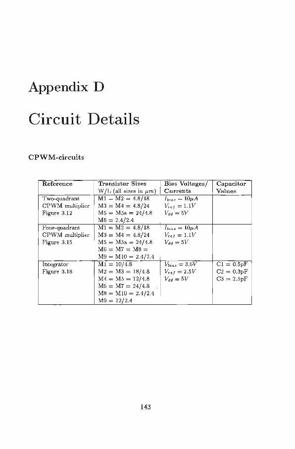
Appendix D
Circuit Details
CPWM-circuits
Reference Transistor Sizes Bias Voltages/ Capacitor W /L (all sizes in pm) Currents Values
Two-quadrant M1 = M2 = 4.8/18 hias = lOJ.JA CPWM multiplier M3 = M4 = 4.8/24 Vref = 1.1V Figure 3.12 MS = MSa = 24/4.8 vdd = sv
M6 = 2.4/2.4 Four-quadrant M1 = M2 = 4.8/18 hias = lOpA CPWM multiplier M3 = M4 = 4.8/24 Vref = 1.1 V Figure 3.15 MS = MSa = 24/4.8 vdd = sv
M6 = M7 = M8 = M9 = MlO = 2.4/2.4
Integrator M1 = 10/4.8 Vbias = 3.6V Cl = O.SpF Figure 3.18 M2 = M3 = 18/4.8 Vref = 2.5V C2 = 0.3pF
M4 = MS = 12/4.8 Vdd = SV C3 = 2.5pF M6 = M7 = 24/4.8 M8 = M10 = 2.4/2.4 M9 = 12/2.4
143

144 APPENDIX D. CIRCUIT DETAILS
Analog Circuits
Reference Transistor Sizes Bias Voltages/ Capacitor W /L (all sizes in 1-lm) Currents Values
Synapse Ml = M2 = 4.8/18 Vref = 2.5V Figure 3.28 M3 = M4 = Vw2 = O.SV
MS = M6 = 4.8/4.8 foias = 20!-lA M7 = M8 = 48/4.8 vdd = sv M9 = MlO = 6/10 Mll = Ml2 = 10/10
Neuron Ml = 10/4.8 /oiasl = 10!-lA C = lpF Figure 3.35 M2 = 30/4.8 /oias2 = 10!-lA
M3 = M4 = 8/12 /oias3 = 3.7/-lA M5 = M6 = 48/4.8 Vref = 2.5V M7 = M8 = 24/4.8 vdd = sv M9 = MlO = 4.8/32 Mll = Ml2 = 8/12 Ml3 = Ml4 = 8/4.8 MIS = Ml6 = 4.8/12 Ml7 = Ml8 = 8/4.8 Ml9 = 75/2.4 M20 = M21 = 12/4.8 M22 = 4.8/8 M23 = 4.8/24 M24 = M25 = 12/4.8 M26 = 150/2.4

Acknowledgements
Constructing acknowledgements is not an easy task and I am bound to forget to mention some people who contributed, more or less, to the completion of this work. To all those people: thanks and I hope nobody will feel left out if his/her name is not mentioned below.
I would like to thank Professor Wim van Bokhoven for giving me the opportunity to perform research within his group on this fascinating subject. I hope the work will be continued with new PhD and graduate students. I am greatly indebted to my copromotor and supervisor Hans Hegt for all the fruitful discussions and useful directions. Together we ran into numerous problems and in all cases we were able to solve them in close cooperation. Without him I wouldn't have been able to finish this work.
Special thanks to Leo Reyneri for an interesting international cooperation on several papers and (a lot of) useful comments on an earlier version of this thesis. Also to Marcello Chiaberge with whom I performed part of the research for this thesis and visited several conferences in interesting places.
The environment in which someone is able to perform is very important and therefore I would like to thank my room mates Gerard Egelmeers and Daniel Schobben and all other members of the Electronic Circuit Design group for a stimulating and most enjoyable environment to work in.
I would like to mention Rene Mol. I feel like we have been able to give each other relaxing moments when we both needed it most. Thanks.
Finally, the persons who should actually be on the top of the list but it seems to be customary to mention the most important ones last. I am very grateful to my parents who always supported me and gave me the freedom to do what I most liked. And my girlfriend Anne-Marie, without her none of this work could have been accomplished.
145

Curriculum Vitae
Heini Withagen was born on April 26, 1969 in Bergen op Zoom, the Netherlands. He graduated from Het Moller Lyceum in 1987. He received the Ir. degree with honours, specialized in Information Technology, from the Department of Electrical Engineering at the Eindhoven University of Technology in 1992. For his master thesis, he spent 8 months with Laboratoires d'Electronique Philips, France working on the recognition of handwritten symbols for use in handheld computers.
From 1992 to 1996, he worked as a Ph.D. student at the Eindhoven University of Technology in the Electronic Circuit Design Group on the hardware implementation of neural networks using analog electronics.
At the beginning of 1995, he started his own company active in the field of consulting and software development for UNIX and Internet applications. Since autumn 1993, he has been the maintainer of one of the main overviews of Internet activity in the Netherlands.
Since October 1996, he has been working for Netcast (formerly known as Riverland Networks), the Netherlands as a project manager and consultant for large Internet and Intranet applications.
147

STELLING EN
Behorende bij het proefschrift
Neural Networks: Analog VLSI Implementation and Learning Algorithms
door H.C.A.M. Withagen
1. De aanname van een klein aantal gewichten per neuron in onderstaande analyse vermindert de waarde van de analyse aangezien de effecten van kwantisatie meer invloed hebben bij een groat aantal gewichten per neuron. (Y. Xie, M.A. Jabri, 'Analysis of the Effects of Quantization in Multilayer Neural Networks using a Statistical Model', IEEE Trans. on Neural Networks, Vol. 3, No. 2, pp. 334-338, 1992)
2. Gezien de plaats van de verwerkingskracht in beide systemen zal een beter inzicht in het leerproces van kunstmatige neurale netwerken het programmeren van parallele computers met hedendaagse CISC/RISC processoren vereenvoudigen.
3. On-chip analoge implementatie van het 'back-propagation' leeralgoritme heeft, onder de huidige technologische randvoorwaarden, zowel vanuit technisch als commercieel oogpunt geen voorkeur. (Dit proefschrift, hoofdstuk 4)
4. De simulatie-resultaten in onderstaand artikel zijn, zelfs met de originele software van de auteurs, niet reproduceerbaar. (K.P. Unnikrishnan, K.P. Venugopal, 'Learning in Connectionist Network using the Alopex Algorithm', Proc. IEEE/INNS Joint Conf. on Neural Networks, pp. 926-931, 1992)
5. De huidige tendens om steeds grotere rekenkracht in te zetten om door grate hoeveelheden informatie te zoeken (data-mining), is in· sommige gevallen onnodig. Een versnelling kan oak verkregen worden door meer structuur in de informatie aan te brengen.

6. Een Darwinistische kijk op geneeskunde zou onderdeel moeten zijn van de opleiding van iedereen werkzaam in deze discipline. (R.M. Nesse, G.C. Williams, 'Why We Get Sick: the new science of Darwinian Medicine', New York, 1995, ISBN 0-8129-2224-7)
7. Ret samenwerken met minder-validen tijdens de aanleg van publieke voorzieningen zal zowel de werkloosheid onder deze groep verlagen als mede de kwaliteit van de voorzieningen verhogen.
8. Autonome zoekrobots op het Internet bezitten op dit moment te weinig intelligentie om de gemiddelde gebruiker goed van dienst te zijn.
9. Ret aanbrengen van veranderingen op het laatste moment komt het eindresultaat meestal niet ten goede.
10. De naam 'Dolly' is sinds de experimenten met klonen niet meer bruikbaar als meisjesnaam.