Embed Size (px)
Citation preview

Journal of Physics Conference Series
OPEN ACCESS
Negative admittance in resistive metal oxide gassensorsTo cite this article A Varpula et al 2008 J Phys Conf Ser 100 082036
View the article online for updates and enhancements
You may also likeLimitation of Atmospheric Composition byCombustionndashExplosion in ExoplanetaryAtmospheresJ L Grenfell S Gebauer M Godolt et al
-
Online Modelling of Heat TransferSolidification and Microstructure inContinuous Casting of SteelS Louhenkilpi J Miettinen J Laine et al
-
Recycling of concrete from demolishedbridges and other engineered structuresT Dettenborn I Harju J Forsman et al
-
This content was downloaded from IP address 2231774174 on 31012022 at 0341
Negative admittance in resistive metal oxide gas
sensors
Aapo Varpula1 Sergey Novikov1 Juha Sinkkonen1 Mikko Utriainen2
1Helsinki University of Technology PO Box 3500 FIN-02015 TKK Espoo Finland2Environics Oy PO Box 349 50101 Mikkeli Finland
E-mail aapovarpulahutfi
Abstract The negative admittance effect is observed in a WO3-based resistive gas sensorMOS1 from Environics Oy The effect is caused by electron trapping (ie oxygen ionization) atthe grain boundary The results show that the current component related to the modulation ofthe grain-boundary barrier dominates in dry clean air and the charging or discharging currentdominates in humid air conditions An equivalent electrical circuit model for the sensor responseis presented
1 Introduction
Resistive gas sensors are typically based on granular semiconductor materials in which electricalconduction is limited by high impedance potential barriers associated with grain boundaries [1]Conductance is exponentially dependent on potential barrier height This is in turn controlledby the grain boundary charge which is modulated by chemical reactions mainly by the oxygenionization Barrier limited conduction provides sensitive monitoring of gas reactions
Time-dependent phenomena in granular gas sensor materials cover a very broad time scalefrom nanoseconds to hours From electrical point of view granular material is a random resistor-capacitor network which shows frequency dispersion in admittance typically in MHz-region [2]The oxygen ionization reaction (ie electron trapping) is an additional effect in sensor materialwhich is usually orders of magnitude slower Impedance spectroscopy is an effective tool tostudy electrical properties of granular materials In this paper we focus on low frequency regimewhere the electronic trapping occurs
A structure where electrons can be trapped at grain boundaries has interesting electricalproperties Introduction of current in material injects free carriers at barrier top This leads toincrease of grain boundary charge by trapping which in turn modulates the current passingthrough the grain-boundary region It turns out that this effect can be represented by aseries resistor-inductor or RL electrical equivalent circuit model with negative circuit elementvalues Usually electron trapping can represented with a series RC electrical equivalent circuitmodel with positive circuit element values However the analysis of electron trapping at grainboundary gives a series RC circuit with negative circuit element values This is caused bynegative polarization of the grain-boundary structure due to the application of voltage
This type of negative admittance or negative capacitance (NC) or anomalous inductive effecthas been earlier reported in various semiconductor devices and materials [3 4 2] eg organiclight-emitting diodes ZnO varistors quantum well infrared photodetectors etc In SnO2 NC
IVC-17ICSS-13 and ICN+T2007 IOP PublishingJournal of Physics Conference Series 100 (2008) 082036 doi1010881742-65961008082036
ccopy 2008 IOP Publishing Ltd 1
has been observed by Varghese et al [5] and Kaur et al [6] Both of the groups explained thephenomenon by the movement of adsorbed ions In this paper we show that the effect can alsobe explained with the barrier limited conduction and electron trapping models
2 Model
Electrical conduction in grain-structured metal-oxide film can be calculated using the drift-diffusion theory [1 7] In the calculation it is assumed that the n-type semiconducting film hasNbarr serially connected identical grain boundaries and the donors are fully ionized The grain-boundary charge density NB is related to the potential barrier height or the surface potential Vs
as Vs =qN2
B
8εNd where q is the electron charge Nd the donor density and ε the permittivity of the
material respectively NB is determined by the oxygen ionization reaction between the adsorbed
oxygen and the free electrons Oads +eminusfree
kiminusrarrlarrminuskminusi
Ominusads
[8 9] which correponds to the rate equation
dNBdt = kinB
(
N totO
minus NB
)
minus kminusiNB Here ki and kminusi are the forward and backward reactionrates and N tot
Othe total density of oxygen (assumed constant) respectively The electron
density at the grain-boundaries is given by nB = Nd exp (minusqVs(kBT )) cosh [qU(2kBTNbarr)]where U is the applied voltage across the film kB Boltzmannrsquos constant and T temperaturerespectively The total current can be written as
Itot = IB minus
U
4NbarrVs
middot Aq middotdNB
dt+
εANd
NBNbarr
middot
dU
dt (1)
Here IB = I0
radic
2Vs0exp (minusqVs(kBT ))sinh[qU (2kBTNbarr)] is the ordinary barrier limited low
frequency current [7] I0 = Amicro(q3N3
dε)05 A the cross-sectional area of the film and micro electronmobility respectively The second term in Eq (1) is arising from charging of traps and thethird term from the current through the depletion layer capacitance Linearization of IB givesthe normal differential conductance and barrier modulation term with negative admittance Bylinearizing Eq (1) an electrical equivalent circuit model shown in Fig 1a is obtained Thecurrent through the two negative admittance circuit branches vanishes at zero bias voltage Thetime constant τ of the negative admittance branches is the same The U dependence of the timeconstant is given by τminus1
prop cosh (qU0(2kBTNbarr)) where U0 is the bias voltage The circuitmodel of Fig 1a without the capacitor C whose admittance is negligible at low frequencies canbe converted into a circuit shown in Fig 1b
CcharRchar
Rdiff
LmodRmod
C
CbRb
Rpar
a)
b)
Figure 1 (a) Electrical equivalent circuit model of the grain-boundarywith a potential barrier C is the normal depletion layer capacitance andRdiff the resistor corresponding to the differential conductance Additionallytwo negative admittance branches are shown The RcharndashCchar branchcorresponds to the charging and discharging current and the RmodndashLmod
branch to the barrier modulation (b) Converted circuit without the capacitorC The values of the elements are given by Rpar = RdiffRmod (Rdiff + Rmod)Rb = RmodRchar (Rmod minus Rchar) and Cb = Cchar (1 minus RcharRmod)
3 Experimental
The studied sample is commercial resistive closed-membrane-type microhotplate gas sensorMOS1 from Environics Oy developed for ChemPro Rcopy100i handheld chemical detector [10]Details of this type of sensor are given in [11] The grain size in the WO3-based coating ofthe sensors is one micrometer or less The sensor was heated to 300oC
IVC-17ICSS-13 and ICN+T2007 IOP PublishingJournal of Physics Conference Series 100 (2008) 082036 doi1010881742-65961008082036
2
The admittance spectra in sub-hertz region were measured with a special measurementscheme A Labview program varies the voltage of a Keithley 236 unit which also measures thecurrent The applied voltage signal consists of a constant DC bias and a uniformly distributedpseudorandom (having flat power spectral density) components The admittance spectra werecalculated from the recorded current and voltage signals by using an fast Fourier transform(FFT) algorithm with a Hanning window The correct operation of the measurement schemewas verified by a test circuit built from commercial passive components Clean air (0ndash40 relative humidity (RH)) was produced by a humidifier and a compressed air system The airflow through the sensor was kept at 02 lmin The sensor was placed in a hermetically sealedmetallic box during the measurements with humid air In the measurements with dry air thesensor was connected directly to the air system
2 25 3
x 10minus5
minus3
minus2
minus1
0
1
2
3
x 10minus6
real Y (S)
imageY
(S
)
ColeminusCole plot
10minus4
10minus3
10minus2
10minus1
100
16
18
2
22
24x 10
minus5
f (Hz)
realY
(S
)
Real part of admittance
10minus4
10minus3
10minus2
10minus1
100
0
05
1
15
2
25x 10
minus6
f (Hz)
imageY
(S
)
Imaginary part of admittance
MeasuredCalculated
Rdiff
= 491 kΩR
mod = minus366 kΩ
Lmod
= minus472 kHR
char = minus347 TΩ
Cchar
= minus037 pF
τ = 129 s
Nbarr
= 247V
s(U = 0) = 105 V
NB(U = 0)Ntot
O = 989 k
minusi = 000263 sminus1
I0 = 215 kAVminus05
σ = qmicroNd = 380 Sm
T = 300oC εr = 4
Equivalent circuitparameters
Model parameters
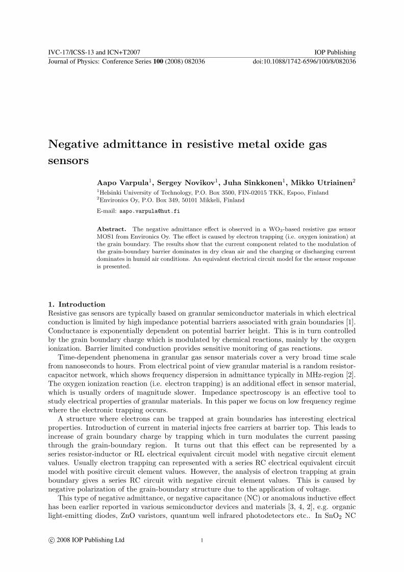
Figure 2 Admittance spectrum of MOS1 sensor in dry clean air at 300oC The maximum ofthe pseudorandom voltage is 200 mV The fit of the equivalent circuit model of Fig 1a is shownby the black solid line
Figure 3 Admittance spectra of MOS1 sensor at various bias voltages in clean humid air (30ndash40 RH) at 300oC The data with 000ndash100 V bias were measured with maximum pseudorandomvoltage of 50 mV and the others with 200 mV The fits of the equivalent circuit model of Fig 1bare shown by black solid lines The values of the circuit elements are shown in Fig 4
4 Results and discussion
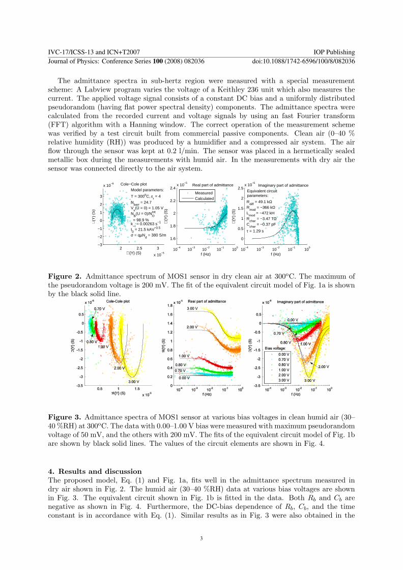
The proposed model Eq (1) and Fig 1a fits well in the admittance spectrum measured indry air shown in Fig 2 The humid air (30ndash40 RH) data at various bias voltages are shownin Fig 3 The equivalent circuit shown in Fig 1b is fitted in the data Both Rb and Cb arenegative as shown in Fig 4 Furthermore the DC-bias dependence of Rb Cb and the timeconstant is in accordance with Eq (1) Similar results as in Fig 3 were also obtained in the
IVC-17ICSS-13 and ICN+T2007 IOP PublishingJournal of Physics Conference Series 100 (2008) 082036 doi1010881742-65961008082036
3
0 1 2 3
-3000-2500-2000-1500-1000-500
200
400
Re
sis
tan
ce
(kΩ
)
Bias voltage U0 (V)
Rpar
Rb
0 1 2 3
-26
-24
-22
-20
-18
-16
-14
Ca
pa
cita
nce
(microF
)
U0 (V)
Cb
1 2 3 4
0
50
100
150
200
250
300
T = 300 oC
Nbarr
= 247
a = 308 mHzb = -265 mHz
τ-1
τ-1 (
mH
z)
U0 (V)
a cosh(qU0(2k
BTN
barr))+b
Figure 4 Values of theresistors the capacitor Cb andthe time constant τ = RbCb ofthe equivalent circuit model ofFig 1b as a function of the biasvoltage
measurements performed at higher frequencies (5 Hz ndash 1 kHz) with a HP4192A impedanceanalyzer and SnO2-based sensor MOS3 from Environics Oy
Figs 2 and 3 the real part of the admittance is positive which indicates that it is dominatedby Rdiff In dry air Fig 2 the imaginary part of admittance is positive whereas in humid airFig 3 it is negative This indicates that the barrier modulation RmodndashLmod branch dominatesin dry air and the charging branch in humid air conditions
In order to explain the spectra measured in humid air the proposed model Eq (1) shouldhave an extraordinary high charging and discharging term This suggests that the trappingtakes place in a much larger area than the path of the current or indicating ion movement alongthe grain boundaries However the bias voltage dependence of the values of the circuit elementsand the time constant is in agreement with the proposed model Eq (1) In [5 6] the negativeadmittance effect was explained by the movement of ions alone However the proposed modeland our results suggest that the main causes of the negative admittance effect are the barriermodulation and the polarization properties of the grain-boundary region and the ions provideenhancement of the charging and discharging component only
5 Conclusions
The negative admittance effect was observed in a WO3-based resistive gas sensor MOS1 fromEnvironics Oy The effect is caused by electron trapping at the grain boundary The results showthat the current component related to the modulation of the grain-boundary barrier dominatesin dry clean air and the charging or discharging current dominates in humid air The sensorresponse in dry clean air can be explained by the proposed model but ion motion is needed inorder to explain the strong charging current in humid air However the bias voltage dependenceof the admittance is in agreement with the proposed model
Acknowledgments
This work was supported by the Nordic Innovation Centre and the Academy of Finland
References[1] Barsan N and Weimar U 2001 J Electroceramics 7 143ndash67[2] Greuter F Blatter G 1990 Semicond Sci Technol 5 111ndash37[3] Ershov M Liu H C Li L Buchanan M Wasilewski Z R and Jonscher A K 1998 IEEE Trans Elec Dev 45
10 2196ndash206[4] Pingree L S C Scott B J Russell M T Marks T J and Hersam M C 2005 Appl Phys Lett 86 073509[5] Varghese O K and Malhotra L K 2000 J Appl Phys 87 10 7457ndash65[6] Kaur M Gupta S K Betty C A Saxena V Katti V R Gadkari S C and Yakhmi J V 2005 Sens Actuators
B 107 360ndash5[7] Sinkkonen J 1980 Phys Stat Sol (b) 102 621ndash7[8] Fort A Rocchi S Serrano-Santos M B Spinicci R and Vignoli V 2006 IEEE Trans Instr Meas 55 6 2102ndash6[9] Ionescu R Llobet E Al-Khalifa S Gardner J W Vilanova X Brezmes J and Correig X 2003 Sens Actuators
B 95 203ndash11[10] Environics Oy httpwwwenvironicsfi
[11] Simon I Barsan N Bauer M and Weimar U 2001 Sens Actuators B 73 1ndash26
IVC-17ICSS-13 and ICN+T2007 IOP PublishingJournal of Physics Conference Series 100 (2008) 082036 doi1010881742-65961008082036
4
Negative admittance in resistive metal oxide gas
sensors
Aapo Varpula1 Sergey Novikov1 Juha Sinkkonen1 Mikko Utriainen2
1Helsinki University of Technology PO Box 3500 FIN-02015 TKK Espoo Finland2Environics Oy PO Box 349 50101 Mikkeli Finland
E-mail aapovarpulahutfi
Abstract The negative admittance effect is observed in a WO3-based resistive gas sensorMOS1 from Environics Oy The effect is caused by electron trapping (ie oxygen ionization) atthe grain boundary The results show that the current component related to the modulation ofthe grain-boundary barrier dominates in dry clean air and the charging or discharging currentdominates in humid air conditions An equivalent electrical circuit model for the sensor responseis presented
1 Introduction
Resistive gas sensors are typically based on granular semiconductor materials in which electricalconduction is limited by high impedance potential barriers associated with grain boundaries [1]Conductance is exponentially dependent on potential barrier height This is in turn controlledby the grain boundary charge which is modulated by chemical reactions mainly by the oxygenionization Barrier limited conduction provides sensitive monitoring of gas reactions
Time-dependent phenomena in granular gas sensor materials cover a very broad time scalefrom nanoseconds to hours From electrical point of view granular material is a random resistor-capacitor network which shows frequency dispersion in admittance typically in MHz-region [2]The oxygen ionization reaction (ie electron trapping) is an additional effect in sensor materialwhich is usually orders of magnitude slower Impedance spectroscopy is an effective tool tostudy electrical properties of granular materials In this paper we focus on low frequency regimewhere the electronic trapping occurs
A structure where electrons can be trapped at grain boundaries has interesting electricalproperties Introduction of current in material injects free carriers at barrier top This leads toincrease of grain boundary charge by trapping which in turn modulates the current passingthrough the grain-boundary region It turns out that this effect can be represented by aseries resistor-inductor or RL electrical equivalent circuit model with negative circuit elementvalues Usually electron trapping can represented with a series RC electrical equivalent circuitmodel with positive circuit element values However the analysis of electron trapping at grainboundary gives a series RC circuit with negative circuit element values This is caused bynegative polarization of the grain-boundary structure due to the application of voltage
This type of negative admittance or negative capacitance (NC) or anomalous inductive effecthas been earlier reported in various semiconductor devices and materials [3 4 2] eg organiclight-emitting diodes ZnO varistors quantum well infrared photodetectors etc In SnO2 NC
IVC-17ICSS-13 and ICN+T2007 IOP PublishingJournal of Physics Conference Series 100 (2008) 082036 doi1010881742-65961008082036
ccopy 2008 IOP Publishing Ltd 1
has been observed by Varghese et al [5] and Kaur et al [6] Both of the groups explained thephenomenon by the movement of adsorbed ions In this paper we show that the effect can alsobe explained with the barrier limited conduction and electron trapping models
2 Model
Electrical conduction in grain-structured metal-oxide film can be calculated using the drift-diffusion theory [1 7] In the calculation it is assumed that the n-type semiconducting film hasNbarr serially connected identical grain boundaries and the donors are fully ionized The grain-boundary charge density NB is related to the potential barrier height or the surface potential Vs
as Vs =qN2
B
8εNd where q is the electron charge Nd the donor density and ε the permittivity of the
material respectively NB is determined by the oxygen ionization reaction between the adsorbed
oxygen and the free electrons Oads +eminusfree
kiminusrarrlarrminuskminusi
Ominusads
[8 9] which correponds to the rate equation
dNBdt = kinB
(
N totO
minus NB
)
minus kminusiNB Here ki and kminusi are the forward and backward reactionrates and N tot
Othe total density of oxygen (assumed constant) respectively The electron
density at the grain-boundaries is given by nB = Nd exp (minusqVs(kBT )) cosh [qU(2kBTNbarr)]where U is the applied voltage across the film kB Boltzmannrsquos constant and T temperaturerespectively The total current can be written as
Itot = IB minus
U
4NbarrVs
middot Aq middotdNB
dt+
εANd
NBNbarr
middot
dU
dt (1)
Here IB = I0
radic
2Vs0exp (minusqVs(kBT ))sinh[qU (2kBTNbarr)] is the ordinary barrier limited low
frequency current [7] I0 = Amicro(q3N3
dε)05 A the cross-sectional area of the film and micro electronmobility respectively The second term in Eq (1) is arising from charging of traps and thethird term from the current through the depletion layer capacitance Linearization of IB givesthe normal differential conductance and barrier modulation term with negative admittance Bylinearizing Eq (1) an electrical equivalent circuit model shown in Fig 1a is obtained Thecurrent through the two negative admittance circuit branches vanishes at zero bias voltage Thetime constant τ of the negative admittance branches is the same The U dependence of the timeconstant is given by τminus1
prop cosh (qU0(2kBTNbarr)) where U0 is the bias voltage The circuitmodel of Fig 1a without the capacitor C whose admittance is negligible at low frequencies canbe converted into a circuit shown in Fig 1b
CcharRchar
Rdiff
LmodRmod
C
CbRb
Rpar
a)
b)
Figure 1 (a) Electrical equivalent circuit model of the grain-boundarywith a potential barrier C is the normal depletion layer capacitance andRdiff the resistor corresponding to the differential conductance Additionallytwo negative admittance branches are shown The RcharndashCchar branchcorresponds to the charging and discharging current and the RmodndashLmod
branch to the barrier modulation (b) Converted circuit without the capacitorC The values of the elements are given by Rpar = RdiffRmod (Rdiff + Rmod)Rb = RmodRchar (Rmod minus Rchar) and Cb = Cchar (1 minus RcharRmod)
3 Experimental
The studied sample is commercial resistive closed-membrane-type microhotplate gas sensorMOS1 from Environics Oy developed for ChemPro Rcopy100i handheld chemical detector [10]Details of this type of sensor are given in [11] The grain size in the WO3-based coating ofthe sensors is one micrometer or less The sensor was heated to 300oC
IVC-17ICSS-13 and ICN+T2007 IOP PublishingJournal of Physics Conference Series 100 (2008) 082036 doi1010881742-65961008082036
2
The admittance spectra in sub-hertz region were measured with a special measurementscheme A Labview program varies the voltage of a Keithley 236 unit which also measures thecurrent The applied voltage signal consists of a constant DC bias and a uniformly distributedpseudorandom (having flat power spectral density) components The admittance spectra werecalculated from the recorded current and voltage signals by using an fast Fourier transform(FFT) algorithm with a Hanning window The correct operation of the measurement schemewas verified by a test circuit built from commercial passive components Clean air (0ndash40 relative humidity (RH)) was produced by a humidifier and a compressed air system The airflow through the sensor was kept at 02 lmin The sensor was placed in a hermetically sealedmetallic box during the measurements with humid air In the measurements with dry air thesensor was connected directly to the air system
2 25 3
x 10minus5
minus3
minus2
minus1
0
1
2
3
x 10minus6
real Y (S)
imageY
(S
)
ColeminusCole plot
10minus4
10minus3
10minus2
10minus1
100
16
18
2
22
24x 10
minus5
f (Hz)
realY
(S
)
Real part of admittance
10minus4
10minus3
10minus2
10minus1
100
0
05
1
15
2
25x 10
minus6
f (Hz)
imageY
(S
)
Imaginary part of admittance
MeasuredCalculated
Rdiff
= 491 kΩR
mod = minus366 kΩ
Lmod
= minus472 kHR
char = minus347 TΩ
Cchar
= minus037 pF
τ = 129 s
Nbarr
= 247V
s(U = 0) = 105 V
NB(U = 0)Ntot
O = 989 k
minusi = 000263 sminus1
I0 = 215 kAVminus05
σ = qmicroNd = 380 Sm
T = 300oC εr = 4
Equivalent circuitparameters
Model parameters
Figure 2 Admittance spectrum of MOS1 sensor in dry clean air at 300oC The maximum ofthe pseudorandom voltage is 200 mV The fit of the equivalent circuit model of Fig 1a is shownby the black solid line
Figure 3 Admittance spectra of MOS1 sensor at various bias voltages in clean humid air (30ndash40 RH) at 300oC The data with 000ndash100 V bias were measured with maximum pseudorandomvoltage of 50 mV and the others with 200 mV The fits of the equivalent circuit model of Fig 1bare shown by black solid lines The values of the circuit elements are shown in Fig 4
4 Results and discussion
The proposed model Eq (1) and Fig 1a fits well in the admittance spectrum measured indry air shown in Fig 2 The humid air (30ndash40 RH) data at various bias voltages are shownin Fig 3 The equivalent circuit shown in Fig 1b is fitted in the data Both Rb and Cb arenegative as shown in Fig 4 Furthermore the DC-bias dependence of Rb Cb and the timeconstant is in accordance with Eq (1) Similar results as in Fig 3 were also obtained in the
IVC-17ICSS-13 and ICN+T2007 IOP PublishingJournal of Physics Conference Series 100 (2008) 082036 doi1010881742-65961008082036
3
0 1 2 3
-3000-2500-2000-1500-1000-500
200
400
Re
sis
tan
ce
(kΩ
)
Bias voltage U0 (V)
Rpar
Rb
0 1 2 3
-26
-24
-22
-20
-18
-16
-14
Ca
pa
cita
nce
(microF
)
U0 (V)
Cb
1 2 3 4
0
50
100
150
200
250
300
T = 300 oC
Nbarr
= 247
a = 308 mHzb = -265 mHz
τ-1
τ-1 (
mH
z)
U0 (V)
a cosh(qU0(2k
BTN
barr))+b
Figure 4 Values of theresistors the capacitor Cb andthe time constant τ = RbCb ofthe equivalent circuit model ofFig 1b as a function of the biasvoltage
measurements performed at higher frequencies (5 Hz ndash 1 kHz) with a HP4192A impedanceanalyzer and SnO2-based sensor MOS3 from Environics Oy
Figs 2 and 3 the real part of the admittance is positive which indicates that it is dominatedby Rdiff In dry air Fig 2 the imaginary part of admittance is positive whereas in humid airFig 3 it is negative This indicates that the barrier modulation RmodndashLmod branch dominatesin dry air and the charging branch in humid air conditions
In order to explain the spectra measured in humid air the proposed model Eq (1) shouldhave an extraordinary high charging and discharging term This suggests that the trappingtakes place in a much larger area than the path of the current or indicating ion movement alongthe grain boundaries However the bias voltage dependence of the values of the circuit elementsand the time constant is in agreement with the proposed model Eq (1) In [5 6] the negativeadmittance effect was explained by the movement of ions alone However the proposed modeland our results suggest that the main causes of the negative admittance effect are the barriermodulation and the polarization properties of the grain-boundary region and the ions provideenhancement of the charging and discharging component only
5 Conclusions
The negative admittance effect was observed in a WO3-based resistive gas sensor MOS1 fromEnvironics Oy The effect is caused by electron trapping at the grain boundary The results showthat the current component related to the modulation of the grain-boundary barrier dominatesin dry clean air and the charging or discharging current dominates in humid air The sensorresponse in dry clean air can be explained by the proposed model but ion motion is needed inorder to explain the strong charging current in humid air However the bias voltage dependenceof the admittance is in agreement with the proposed model
Acknowledgments
This work was supported by the Nordic Innovation Centre and the Academy of Finland
References[1] Barsan N and Weimar U 2001 J Electroceramics 7 143ndash67[2] Greuter F Blatter G 1990 Semicond Sci Technol 5 111ndash37[3] Ershov M Liu H C Li L Buchanan M Wasilewski Z R and Jonscher A K 1998 IEEE Trans Elec Dev 45
10 2196ndash206[4] Pingree L S C Scott B J Russell M T Marks T J and Hersam M C 2005 Appl Phys Lett 86 073509[5] Varghese O K and Malhotra L K 2000 J Appl Phys 87 10 7457ndash65[6] Kaur M Gupta S K Betty C A Saxena V Katti V R Gadkari S C and Yakhmi J V 2005 Sens Actuators
B 107 360ndash5[7] Sinkkonen J 1980 Phys Stat Sol (b) 102 621ndash7[8] Fort A Rocchi S Serrano-Santos M B Spinicci R and Vignoli V 2006 IEEE Trans Instr Meas 55 6 2102ndash6[9] Ionescu R Llobet E Al-Khalifa S Gardner J W Vilanova X Brezmes J and Correig X 2003 Sens Actuators
B 95 203ndash11[10] Environics Oy httpwwwenvironicsfi
[11] Simon I Barsan N Bauer M and Weimar U 2001 Sens Actuators B 73 1ndash26
IVC-17ICSS-13 and ICN+T2007 IOP PublishingJournal of Physics Conference Series 100 (2008) 082036 doi1010881742-65961008082036
4
0 1 2 3
-3000-2500-2000-1500-1000-500
200
400
Re
sis
tan
ce
(kΩ
)
Bias voltage U0 (V)
Rpar
Rb
0 1 2 3
-26
-24
-22
-20
-18
-16
-14
Ca
pa
cita
nce
(microF
)
U0 (V)
Cb
1 2 3 4
0
50
100
150
200
250
300
T = 300 oC
Nbarr
= 247
a = 308 mHzb = -265 mHz
τ-1
τ-1 (
mH
z)
U0 (V)
a cosh(qU0(2k
BTN
barr))+b
Figure 4 Values of theresistors the capacitor Cb andthe time constant τ = RbCb ofthe equivalent circuit model ofFig 1b as a function of the biasvoltage
measurements performed at higher frequencies (5 Hz ndash 1 kHz) with a HP4192A impedanceanalyzer and SnO2-based sensor MOS3 from Environics Oy
Figs 2 and 3 the real part of the admittance is positive which indicates that it is dominatedby Rdiff In dry air Fig 2 the imaginary part of admittance is positive whereas in humid airFig 3 it is negative This indicates that the barrier modulation RmodndashLmod branch dominatesin dry air and the charging branch in humid air conditions
In order to explain the spectra measured in humid air the proposed model Eq (1) shouldhave an extraordinary high charging and discharging term This suggests that the trappingtakes place in a much larger area than the path of the current or indicating ion movement alongthe grain boundaries However the bias voltage dependence of the values of the circuit elementsand the time constant is in agreement with the proposed model Eq (1) In [5 6] the negativeadmittance effect was explained by the movement of ions alone However the proposed modeland our results suggest that the main causes of the negative admittance effect are the barriermodulation and the polarization properties of the grain-boundary region and the ions provideenhancement of the charging and discharging component only
5 Conclusions
The negative admittance effect was observed in a WO3-based resistive gas sensor MOS1 fromEnvironics Oy The effect is caused by electron trapping at the grain boundary The results showthat the current component related to the modulation of the grain-boundary barrier dominatesin dry clean air and the charging or discharging current dominates in humid air The sensorresponse in dry clean air can be explained by the proposed model but ion motion is needed inorder to explain the strong charging current in humid air However the bias voltage dependenceof the admittance is in agreement with the proposed model
Acknowledgments
This work was supported by the Nordic Innovation Centre and the Academy of Finland
References[1] Barsan N and Weimar U 2001 J Electroceramics 7 143ndash67[2] Greuter F Blatter G 1990 Semicond Sci Technol 5 111ndash37[3] Ershov M Liu H C Li L Buchanan M Wasilewski Z R and Jonscher A K 1998 IEEE Trans Elec Dev 45
10 2196ndash206[4] Pingree L S C Scott B J Russell M T Marks T J and Hersam M C 2005 Appl Phys Lett 86 073509[5] Varghese O K and Malhotra L K 2000 J Appl Phys 87 10 7457ndash65[6] Kaur M Gupta S K Betty C A Saxena V Katti V R Gadkari S C and Yakhmi J V 2005 Sens Actuators
B 107 360ndash5[7] Sinkkonen J 1980 Phys Stat Sol (b) 102 621ndash7[8] Fort A Rocchi S Serrano-Santos M B Spinicci R and Vignoli V 2006 IEEE Trans Instr Meas 55 6 2102ndash6[9] Ionescu R Llobet E Al-Khalifa S Gardner J W Vilanova X Brezmes J and Correig X 2003 Sens Actuators
B 95 203ndash11[10] Environics Oy httpwwwenvironicsfi
[11] Simon I Barsan N Bauer M and Weimar U 2001 Sens Actuators B 73 1ndash26
IVC-17ICSS-13 and ICN+T2007 IOP PublishingJournal of Physics Conference Series 100 (2008) 082036 doi1010881742-65961008082036
4


![Nanoscale Resistive Switching in ...strukov/papers/2014/AdvFuncMat2014.pdf · [ 5b , 8 ] Nanoscale electromechanical phenomena in functional oxide layers, ranging from fl exoelectricity](https://img.pdfslide.us/doc/110x75/5fc39ae3a436ea4b2b10ff1c/nanoscale-resistive-switching-in-strukovpapers2014advfuncmat2014pdf-.jpg)