Embed Size (px)
Citation preview

NCT7509Y
NCT7509W
Nuvoton Thermal Sensor IC with Fan Control
Date: Aug/15/2012 Revision: 1.0

NCT7509W/NCT7509Y
Release Date: Aug, 2012
- I - Version: 1.0
Table of Content-
1. GENERAL DESCRIPTION ......................................................................................................... 1
2. FEATURES ................................................................................................................................. 1
2.1 Fan Speed Monitoring and Control ............................................................................................ 1
2.2 Temperature Measurement ........................................................................................................ 1
2.3 Event Notification ......................................................................................................................... 1
2.4 General ........................................................................................................................................ 1
3. KEY SPECIFICATIONS .............................................................................................................. 2
4. PIN CONFIGURATION ............................................................................................................... 2
5. PIN DESCRIPTION ..................................................................................................................... 3
5.1 PIN TYPE DISCRIPTION ........................................................................................................... 3
5.2 PIN DISCRIPTION ...................................................................................................................... 3
6. FUNCTION DESCRIPTION ........................................................................................................ 4
6.1 General Description .................................................................................................................... 4
6.2 Access Interface .......................................................................................................................... 4
6.2.1 Data write to the internal register .............................................................................. 4
6.2.2 Data read from the internal register .......................................................................... 4
6.3 Address Setting ........................................................................................................................... 5
6.4 Temperature Measurement Data Format .................................................................................. 5
6.4.1 The local temperature (on-die) data with 8-bit 2`s complement format. .................... 5
6.4.2 The remote temperature data with 11-bit 2`s complement format. ........................... 5
6.5 ALERT# Output ........................................................................................................................... 5
6.5.1 ALERT# Output Comparator Mode .......................................................................... 7
6.5.2 ALERT# Output Interrupt Mode ................................................................................ 7
6.5.3 ALERT# Output SMBusTM
alert Mode ...................................................................... 8
6.6 T_CRIT# Output .......................................................................................................................... 8
6.7 FAN_IN Count Calculation ......................................................................................................... 9
6.8 FAN_OUT Duty Cycle Calculation ............................................................................................. 9
6.9 SMART FANTM
IV Control Parameters ...................................................................................... 9
6.9.1 Step Up Time / Step Down Time .............................................................................. 9
6.9.2 Fan Output Start-up Value ...................................................................................... 10
6.9.3 Fan Output Nonstop Value ..................................................................................... 10
6.9.4 Fan Output Stop Time ............................................................................................ 11
6.10 Speed Cruise Mode ................................................................................................................. 11
6.11 Thermal Cruise Mode .............................................................................................................. 12
6.12 SMART FANTM
IV & Close Loop Fan Control Mode ............................................................. 13
6.13 Dynamic Fast Tracking Feature .............................................................................................. 14
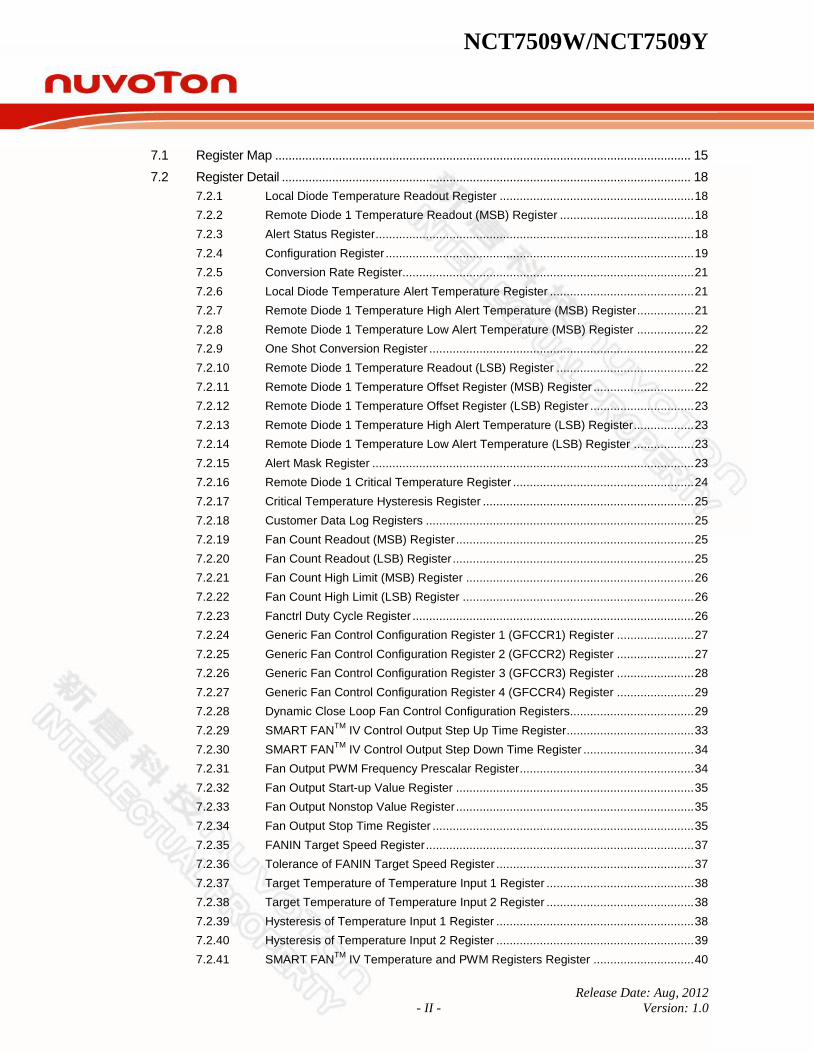
7. REGISTER SUMMARY ............................................................................................................ 15
NCT7509W/NCT7509Y
Release Date: Aug, 2012
- II - Version: 1.0
7.1 Register Map ............................................................................................................................ 15
7.2 Register Detail .......................................................................................................................... 18
7.2.1 Local Diode Temperature Readout Register .......................................................... 18
7.2.2 Remote Diode 1 Temperature Readout (MSB) Register ........................................ 18
7.2.3 Alert Status Register ............................................................................................... 18
7.2.4 Configuration Register ............................................................................................ 19
7.2.5 Conversion Rate Register....................................................................................... 21
7.2.6 Local Diode Temperature Alert Temperature Register ........................................... 21
7.2.7 Remote Diode 1 Temperature High Alert Temperature (MSB) Register ................. 21
7.2.8 Remote Diode 1 Temperature Low Alert Temperature (MSB) Register ................. 22
7.2.9 One Shot Conversion Register ............................................................................... 22
7.2.10 Remote Diode 1 Temperature Readout (LSB) Register ......................................... 22
7.2.11 Remote Diode 1 Temperature Offset Register (MSB) Register .............................. 22
7.2.12 Remote Diode 1 Temperature Offset Register (LSB) Register ............................... 23
7.2.13 Remote Diode 1 Temperature High Alert Temperature (LSB) Register .................. 23
7.2.14 Remote Diode 1 Temperature Low Alert Temperature (LSB) Register .................. 23
7.2.15 Alert Mask Register ................................................................................................ 23
7.2.16 Remote Diode 1 Critical Temperature Register ...................................................... 24
7.2.17 Critical Temperature Hysteresis Register ............................................................... 25
7.2.18 Customer Data Log Registers ................................................................................ 25
7.2.19 Fan Count Readout (MSB) Register ....................................................................... 25
7.2.20 Fan Count Readout (LSB) Register ........................................................................ 25
7.2.21 Fan Count High Limit (MSB) Register .................................................................... 26
7.2.22 Fan Count High Limit (LSB) Register ..................................................................... 26
7.2.23 Fanctrl Duty Cycle Register .................................................................................... 26
7.2.24 Generic Fan Control Configuration Register 1 (GFCCR1) Register ....................... 27
7.2.25 Generic Fan Control Configuration Register 2 (GFCCR2) Register ....................... 27
7.2.26 Generic Fan Control Configuration Register 3 (GFCCR3) Register ....................... 28
7.2.27 Generic Fan Control Configuration Register 4 (GFCCR4) Register ....................... 29
7.2.28 Dynamic Close Loop Fan Control Configuration Registers..................................... 29
7.2.29 SMART FANTM
IV Control Output Step Up Time Register ...................................... 33
7.2.30 SMART FANTM
IV Control Output Step Down Time Register ................................. 34
7.2.31 Fan Output PWM Frequency Prescalar Register .................................................... 34
7.2.32 Fan Output Start-up Value Register ....................................................................... 35
7.2.33 Fan Output Nonstop Value Register ....................................................................... 35
7.2.34 Fan Output Stop Time Register .............................................................................. 35
7.2.35 FANIN Target Speed Register ................................................................................ 37
7.2.36 Tolerance of FANIN Target Speed Register ........................................................... 37
7.2.37 Target Temperature of Temperature Input 1 Register ............................................ 38
7.2.38 Target Temperature of Temperature Input 2 Register ............................................ 38
7.2.39 Hysteresis of Temperature Input 1 Register ........................................................... 38
7.2.40 Hysteresis of Temperature Input 2 Register ........................................................... 39
7.2.41 SMART FANTM
IV Temperature and PWM Registers Register .............................. 40

NCT7509W/NCT7509Y
Release Date: Aug, 2012
- III - Version: 1.0
7.2.42 Remote Diode Temperature Filter and Alert Mode Setting Register ....................... 41
7.2.43 Chip ID Register ..................................................................................................... 41
7.2.44 Vendor ID Register ................................................................................................. 43
7.2.45 Device ID Register .................................................................................................. 43
8. ELECTRICAL CHARACTERISTICS ......................................................................................... 44
8.1 Absolute Maximum Ratings ..................................................................................................... 44
8.2 DC Characteristics ................................................................................................................... 44
8.3 AC Characteristics .................................................................................................................... 45
9. ORDERING INFORMATION ..................................................................................................... 45
10. TOP MARKING SPECIFICATION ............................................................................................ 46
11. PACKAGE DRAWING AND DIMENSIONS .............................................................................. 47
11.1 10L DFN (3X3 MM^2; 0.8 MM) ............................................................................................... 47
11.2 10L MSOP (3X3 MM^2) ........................................................................................................... 48
12. REVISION HISTORY ................................................................................................................ 49
NCT7509W/NCT7509Y
Release Date: Aug, 2012
- 1 - Version: 1.0
1. GENERAL DESCRIPTION
The NCT7509 is a Nuvoton Hardware Monitor IC, contains 1 remote and 1 on-die temperature sensor and 1 fan controller with SMBus
TM interface. The remote sensor is diode-connected transistor, such
as 2N3904 or the thermal diode integrated in Computer Processor Units (CPU) and Graphics Processor Units (GPU). The NCT7509 also supports offset adjust register to correct the errors that casued by different thermal diodes.
The fan controller in NCT7509 support PWM (pulse width modulation) fan output modes for Nuvoton SMART FAN
TM control - “Thermal Cruise
TM“ mode and “SMART FAN
TM IV” mode. In the “Thermal
CruiseTM
“ mode, temperatures of CPU/GPU and the system can be maintained within specific programmable ranges under the hardware control. SMART FAN
TM IV provides 8 sets of temperatures
setting points to program 6 slopes linear fan speed vs. temperature transfer function. NCT7509 also supports close-loop fan controller based on RPM. The NCT7509 provides an easy to implement cooling and quiet solution with maximum safety and flexibility.
The NCT7509 supports 2 wire alert signals which ALERT# is for processor event notification and T_CRIT is for thermal shutdown.
2. FEATURES
2.1 Fan Speed Monitoring and Control
Support 256 steps PWM modes fan speed control
Thermal CruiseTM
“ and SMART FAN™IV to control the fan speed
Enhanced Smart Fan algorithm, SMART FAN™ IV, supports multi-tracking of fan control vs.
temperature and registers for each fan control output.
Closed-loop fan controller via RPM setting
Manual Mode for specific application
2.2 Temperature Measurement
Measure the temperature with high accuracy
One local on-die thermal sensor
One remote temperature sensor with current mode
2.3 Event Notification
Supports 2 alert outputs : ALERT# and T_CRIT#
Event notification via ALERT# signal for over temperature and fan error
ALERT# output supports SMBusTM
2.0 ARA function
T_CRIT# point supports Hardware Power-on setting
2.4 General
I2C® Compatible System Management bus (SMBus
TM)
3.3V±5% VDD operation

NCT7509W/NCT7509Y
Release Date: Aug, 2012
- 2 - Version: 1.0
10-pin MSOP and DFN Green Package (Halogen-free)
3. KEY SPECIFICATIONS
PARAMETER RATING
Local temperature range and accuracy
-40C to +125C
Typ. 2C (20C~40C)
Max. 3C (-40C~125C)*1
Remote temperature range and accuracy
-40C to +127C
Typ. 1C (25C ~70C)
Typ. 2C (-40C ~127C)
Max. 3C (-40C~127C)*2
Supply voltage 3.3V ± 5%
Operating supply current 3 mA typ.
ADC resolution include sign bit 10 Bits
*1 Guaranteed by design from -40~125 degreeC, 100% tested at 85 degreeC.
*2 Guaranteed by design from -40~127 degreeC, 100% tested at 85 degreeC.
4. PIN CONFIGURATION

NCT7509W/NCT7509Y
Release Date: Aug, 2012
- 3 - Version: 1.0
5. PIN DESCRIPTION
5.1 PIN TYPE DISCRIPTION
PIN TYPE PIN ATTRIBUTE
OD12 Open-drain output pin with 12 mA sink capability
INts TTL level input pin and schmitt trigger
AIN Input pin (Analog)
P Power or Ground Pin
5.2 PIN DISCRIPTION
PIN NO. PIN NAME I/O FUNCTION
1 T_CRIT# OD12 T_CRIT alarm output, for interrupt or shutdown control
2 VDD P DC Power supply, Voltage input 3.3V±5%
3 D+ AIN Connect to Thermal Diode Anode
4 D- AIN Connect to Thermal Diode Cathode
5 FAN_OUT OD12 Fan speed control PWM output
6 GND P Power supply ground
7 ALERT# OD12 Alarm output, for interrupt control
8 FAN_IN INts Fan tachometer input
9 SDA INts/ OD12 SMBusTM
bi-directional data
10 SCL INts SMBusTM
Clock

NCT7509W/NCT7509Y
Release Date: Aug, 2012
- 4 - Version: 1.0
6. FUNCTION DESCRIPTION
6.1 General Description
NCT7509 is SMBusTM
interface device to provides on-die temperature sensor and 1 set of thermal inputs for CPU/GPU thermal diode sensor, 2 wire alert signals which ALERT# is for processor event notification and T_CRIT# is for thermal shutdown,1set fan speed input and output which support PWM(Pulse Width Modulation) fan control.
6.2 Access Interface
NCT7509 provides SMBusTM
to access the internal register. It supports SMBusTM
byte write and byte read protocols.
6.2.1 Data write to the internal register
6.2.2 Data read from the internal register

NCT7509W/NCT7509Y
Release Date: Aug, 2012
- 5 - Version: 1.0
6.3 Address Setting
NCT7509 I2C/SMBusTM
address is 1001100xb (x is R/W bit).
6.4 Temperature Measurement Data Format
6.4.1 The local temperature (on-die) data with 8-bit 2`s complement format.
TEMPERATURE 8-BIT DIGITAL OUTPUT
+127°C 0111,1111
+25°C 0001,1001
+2°C 0000,0010
+1°C 0000,0001
+0°C 0000,0000
- 1°C 1111,1111
- 2°C 1111,1110
- 25°C 1110,0111
- 128°C 1000,0000
6.4.2 The remote temperature data with 11-bit 2`s complement format.
TEMPERATURE 8-BIT DIGITAL OUTPUT HIGH BYTE 3-BIT DIGITAL OUTPUT LOW BYTE
+127.875°C 0111,1111 111X,XXXX
+25.750°C 0001,1001 110X,XXXX
+2.250°C 0000,0010 010X,XXXX
+1.125°C 0000,0001 001X,XXXX
+0.000°C 0000,0000 000X,XXXX
- 1.125°C 1111,1110 111X,XXXX
- 2.250°C 1111,1101 110X,XXXX
- 25.750°C 1110,0110 010X,XXXX
- 127.875°C 1000,0000 001X,XXXX
6.5 ALERT# Output
The NCT7509 ALERT# pin is an active-low open-drain output pin which is triggered when measured temperature exceeds the limitation defined in the limit registers. There are three types of ALERT#

NCT7509W/NCT7509Y
Release Date: Aug, 2012
- 6 - Version: 1.0
output mode: the ALERT# output comparator mode, the ALERT# output interrupt mode, and the ALERT# output SMBus
TM ALERT# mode.
NCT7509W/NCT7509Y
Release Date: Aug, 2012
- 7 - Version: 1.0
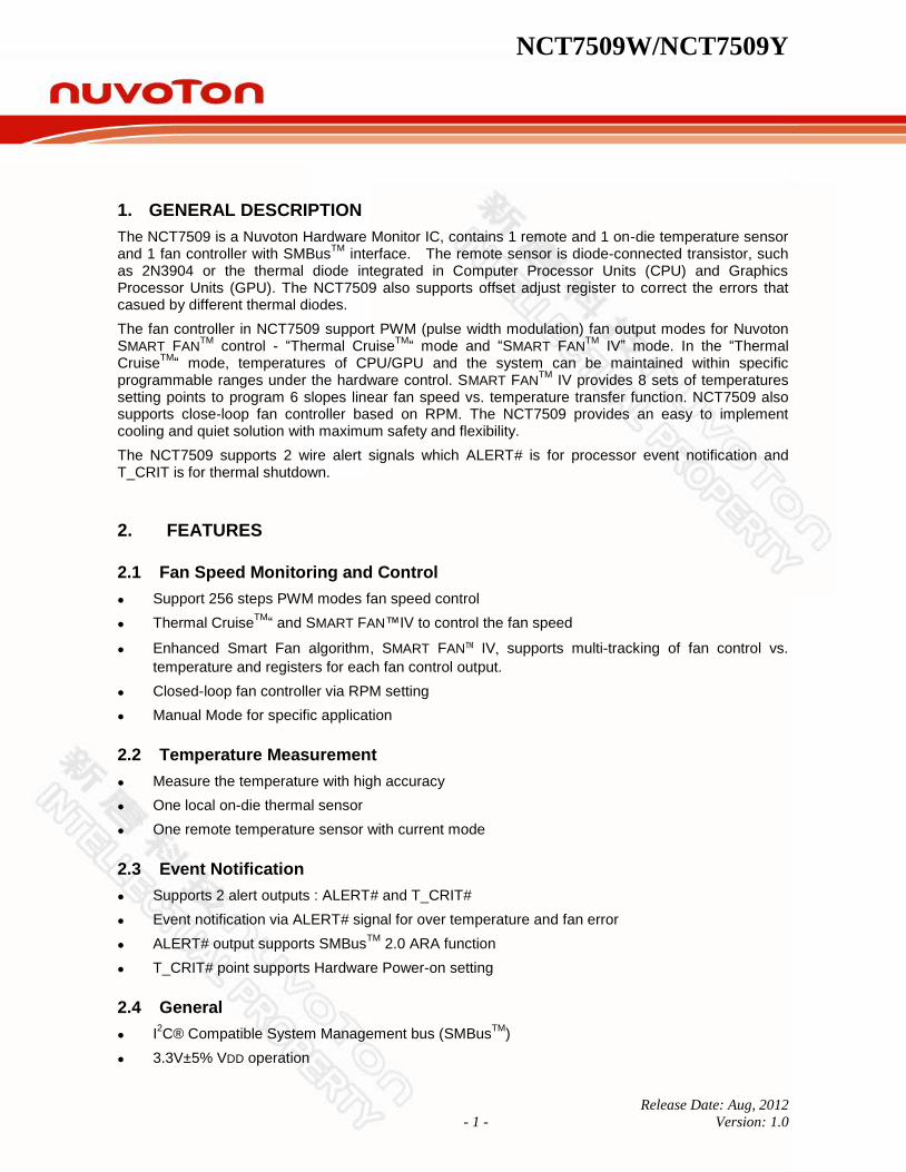
6.5.1 ALERT# Output Comparator Mode
Figure 1 shows the mechanism of the ALERT# output comparator mode. In this mode, the ALERT# pin will be alerted if the monitored temperature is out-of-limit and the ALERT# pin keeps low until the temperature goes back to the target range.
Figure 1
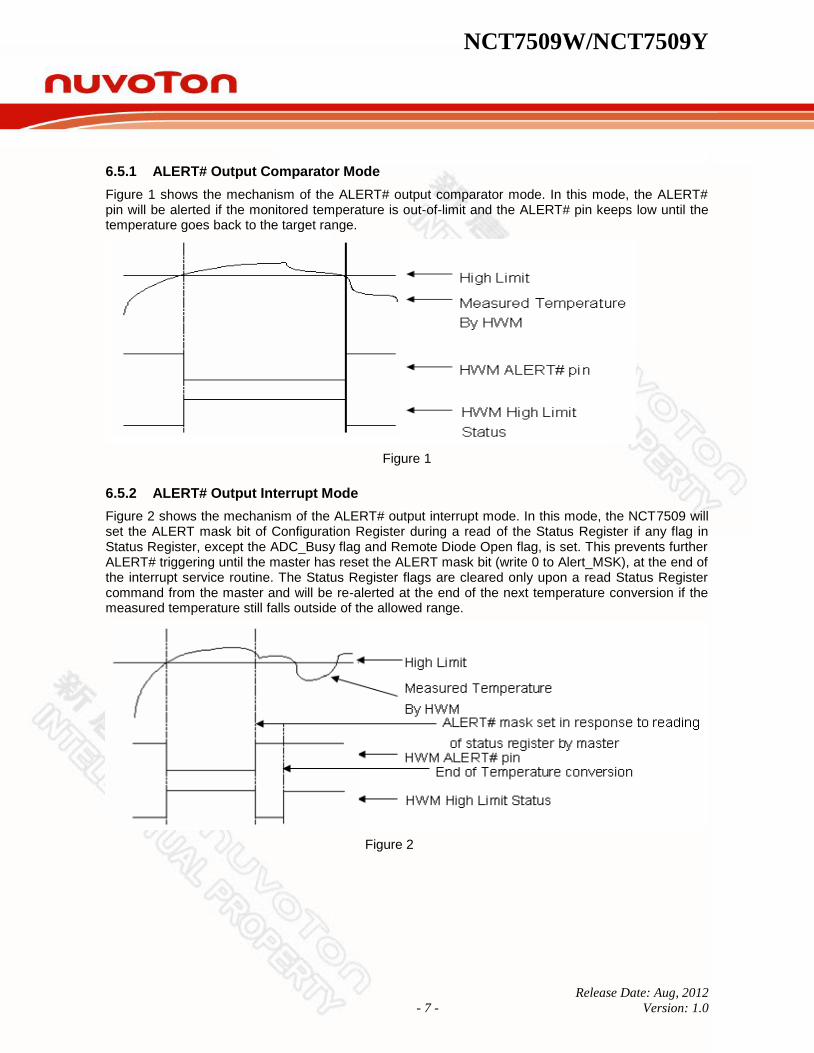
6.5.2 ALERT# Output Interrupt Mode
Figure 2 shows the mechanism of the ALERT# output interrupt mode. In this mode, the NCT7509 will set the ALERT mask bit of Configuration Register during a read of the Status Register if any flag in Status Register, except the ADC_Busy flag and Remote Diode Open flag, is set. This prevents further ALERT# triggering until the master has reset the ALERT mask bit (write 0 to Alert_MSK), at the end of the interrupt service routine. The Status Register flags are cleared only upon a read Status Register command from the master and will be re-alerted at the end of the next temperature conversion if the measured temperature still falls outside of the allowed range.
Figure 2
NCT7509W/NCT7509Y
Release Date: Aug, 2012
- 8 - Version: 1.0
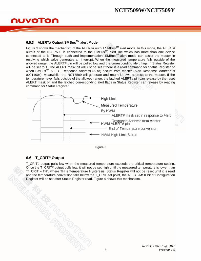
6.5.3 ALERT# Output SMBusTM
alert Mode
Figure 3 shows the mechanism of the ALERT# output SMBusTM
alert mode. In this mode, the ALERT# output of the NCT7509 is connected to the SMBus
TM alert line which has more than one device
connected to it. Through such and implementation, SMBusTM
alert mode can assist the master in resolving which salve generates an interrupt. When the measured temperature falls outside of the allowed range, the ALERT# pin will be pulled low and the corresponding alert flags in Status Register will be set to 1. The ALERT mask bit will just be set if there is a read command for Status Register or when SMBus
TM ALERT Response Address (ARA) occurs from master (Alert Response Address is
0001100x). Meanwhile, the NCT7509 will generate and return its own address to the master. If the temperature never falls outside of the allowed range, the latched ALERT# pin can release by the reset ALERT mask bit and the latched corresponding alert flags in Status Register can release by reading command for Status Register.
Figure 3
6.6 T_CRIT# Output
T_CRIT# output pulls low when the measured temperature exceeds the critical temperature setting. Once the T_CRIT# output pulls low, it will not be set high until the measured temperature is lower than “T_CRIT – TH”, where TH is Temperature Hysteresis. Status Register will not be reset until it is read and the temperature conversion falls below the T_CRIT set point, the ALERT-MSK bit of Configuration Register will be set after Status Register read. Figure 4 shows this mechanism.

NCT7509W/NCT7509Y
Release Date: Aug, 2012
- 9 - Version: 1.0
Figure 4
6.7 FAN_IN Count Calculation
The FAN_IN tachometer high byte and low byte are combined to 12-bitCountValue. Real RPM (Rotate per Minute) calculation should follow the formula:
)4
()12(
1035.1)(
6
FanPolesluebitCountVaRPMSpeedFan
In this formula, FanPoles stands for the number of NS pole pairs inside the fan. Normally an N-S-N-S Fan (FanPoles=4) generates 2 pulses after completing one rotation.
6.8 FAN_OUT Duty Cycle Calculation
The NCT7509 provides 1 set of PWM for fan speed control. The duty cycle of PWM can be programmed by an 8-bit register. The expression of duty cycle can be represented as follow formula:
%100255
ValueRegister bit -8 Programmed(%)cycleDuty
6.9 SMART FANTM
IV Control Parameters
In SMART FANTM
IV Mode, there are some Fan control parameters as below descriptions:
6.9.1 Step Up Time / Step Down Time
SMART FANTM
IV is designed for the smooth operation of the fan. The Up Time / Down Time register defines the time interval between successive duty increases or decreases. If this value is set too small, the fan will not have enough time to speed up after tuning the duty and sometimes may result in unstable fan speed. On the other hand, if Up Time / Down Time is set too large, the fan may not work fast enough to dissipate the heat. This register should never be set to 0, otherwise, the fan duty will be abnormal.

NCT7509W/NCT7509Y
Release Date: Aug, 2012
- 10 - Version: 1.0
6.9.2 Fan Output Start-up Value
From still to rotate, the fan usually needs a higher fan output value to generate enough torque to conquer the restriction force. Thus the Fan Output Start-up Value is used to turn on the fan with the specified output value.
6.9.3 Fan Output Nonstop Value
It takes some time to bring a fan from still to working state. Therefore, Nonstop value are designed with a minimum fan output to keep the fan working when the system does not require the fan to help reduce heat but still want to keep the fast response time to speed up the fan.

NCT7509W/NCT7509Y
Release Date: Aug, 2012
- 11 - Version: 1.0
6.9.4 Fan Output Stop Time
A time interval is specified to turn off the fan if SMART FANTM
IV continuously requests to slow down the fan which has already reached the Stop time.
DownTime
StopTime
UpTimeN
onSt
op
Star
t
Smart Fan Lowering
FanSpeed
Smart Fan Arising Fan
Speed
FanSpeed
Smart Fan Control Parameters Figure
6.10 Speed Cruise Mode
Fan Speed Cruise mode keeps the fan speed in a specified range. This range is defined by a fan
speed count and an interval (e.g., 160 10). As long as the fan speed count is in the specified range, fan output remains the same. If the fan speed count is higher than the high end (e.g., 170), fan output increases to make the count lower. If the fan speed count is lower than the low end (e.g., 150), fan output decreases to make the count higher. One example is illustrated in this figure.
160
170
150
Fan output
100
0
50
A CCount
(%)
Mechanism of Fan Speed CruiseTM
Mode
NCT7509W/NCT7509Y
Release Date: Aug, 2012
- 12 - Version: 1.0
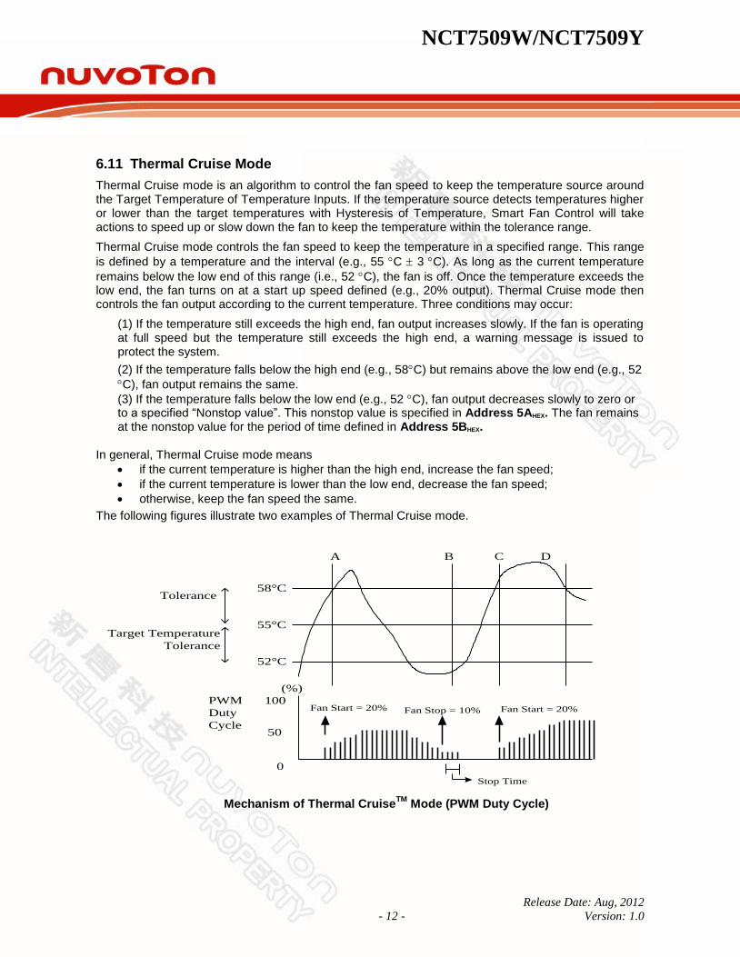
6.11 Thermal Cruise Mode
Thermal Cruise mode is an algorithm to control the fan speed to keep the temperature source around the Target Temperature of Temperature Inputs. If the temperature source detects temperatures higher or lower than the target temperatures with Hysteresis of Temperature, Smart Fan Control will take actions to speed up or slow down the fan to keep the temperature within the tolerance range.
Thermal Cruise mode controls the fan speed to keep the temperature in a specified range. This range
is defined by a temperature and the interval (e.g., 55 C 3 C). As long as the current temperature
remains below the low end of this range (i.e., 52 C), the fan is off. Once the temperature exceeds the low end, the fan turns on at a start up speed defined (e.g., 20% output). Thermal Cruise mode then controls the fan output according to the current temperature. Three conditions may occur:
(1) If the temperature still exceeds the high end, fan output increases slowly. If the fan is operating at full speed but the temperature still exceeds the high end, a warning message is issued to protect the system.
(2) If the temperature falls below the high end (e.g., 58C) but remains above the low end (e.g., 52
C), fan output remains the same.
(3) If the temperature falls below the low end (e.g., 52 C), fan output decreases slowly to zero or to a specified “Nonstop value”. This nonstop value is specified in Address 5AHEX. The fan remains at the nonstop value for the period of time defined in Address 5BHEX.
In general, Thermal Cruise mode means
if the current temperature is higher than the high end, increase the fan speed;
if the current temperature is lower than the low end, decrease the fan speed;
otherwise, keep the fan speed the same.
The following figures illustrate two examples of Thermal Cruise mode.
A B C D
58°C
55°C
52°C
Tolerance
Target Temperature
Tolerance
50
100
0
PWM
Duty
Cycle
(%)
Fan Start = 20% Fan Stop = 10% Fan Start = 20%
Stop Time
Mechanism of Thermal CruiseTM
Mode (PWM Duty Cycle)
NCT7509W/NCT7509Y
Release Date: Aug, 2012
- 13 - Version: 1.0
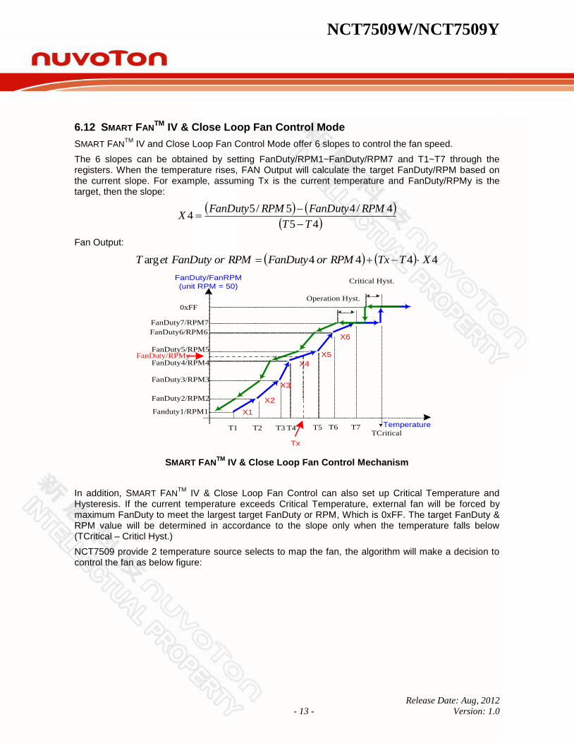
6.12 SMART FANTM
IV & Close Loop Fan Control Mode
SMART FANTM
IV and Close Loop Fan Control Mode offer 6 slopes to control the fan speed.
The 6 slopes can be obtained by setting FanDuty/RPM1~FanDuty/RPM7 and T1~T7 through the registers. When the temperature rises, FAN Output will calculate the target FanDuty/RPM based on the current slope. For example, assuming Tx is the current temperature and FanDuty/RPMy is the target, then the slope:
45
4/45/54
TT
RPMFanDutyRPMFanDutyX
Fan Output:
4444arg XTTxRPMorFanDutyRPMorFanDutyetT
FanDuty/FanRPM
(unit RPM = 50)
Fanduty1/RPM1
FanDuty2/RPM2
FanDuty3/RPM3
FanDuty4/RPM4
FanDuty5/RPM5
FanDuty6/RPM6
FanDuty7/RPM7
0xFF
Operation Hyst.
Critical Hyst.
T1 T2 T3 T4 T5 T6 T7TCritical
Temperature
X1
X4
X5
X3
X2
X6
Tx
FanDuty/RPMy
SMART FANTM
IV & Close Loop Fan Control Mechanism
In addition, SMART FANTM
IV & Close Loop Fan Control can also set up Critical Temperature and Hysteresis. If the current temperature exceeds Critical Temperature, external fan will be forced by maximum FanDuty to meet the largest target FanDuty or RPM, Which is 0xFF. The target FanDuty & RPM value will be determined in accordance to the slope only when the temperature falls below (TCritical – Criticl Hyst.)
NCT7509 provide 2 temperature source selects to map the fan, the algorithm will make a decision to control the fan as below figure:

NCT7509W/NCT7509Y
Release Date: Aug, 2012
- 14 - Version: 1.0
Any Temp request
faster Fan??
Any Temp request f
hold current speed??
No
No
Speed Up
Hold current
Speed
Slow Down
Yes
Yes
6.13 Dynamic Fast Tracking Feature
In the SMART FANTM
IV & Close Loop Control Mode, in order to have a faster Fan Duty update response to external temperature variation, NCT7509 involves a Dynamic Fast Tracking mode. That how fast could be reached is depended on user’s configuration and how rapid temperature variation.
In addition to independent temperature control method, which means that one external fan would be controlled by only one temperature source, NCT7509 also support combined temperature control method. User could conjugate CPU & System temperature with CPU fan to obtain a better thermal management on the system level through this feature.
Per appropriate configuration, fan control response time could come out following behavior.
Tracking Time, t
RPM_Old
RPM_Target
if Tcpu < Tcontrol , Tsys < Tambient
Δt
=> Δt α ƒ( Programmable step change )
CPU Fan RPMCPU Fan RPM
Tracking Time, t
RPM_Old
RPM_Target
if Tcpu > Tcontrol , Tsys < Tambient
Δt
=> Δt α ƒ( RPM_Target - RPM_Old )
CPU Fan RPM
Tracking Time, t
RPM_Old
RPM_Target
if Tcpu > Tcontrol , Tsys > Tambient
Δt
=> Δt α ƒ( Programmable step change,
weighting ,
(Tsys – Tambient) ,
(RPM_Target - RPM_Old) )
Tracking Time, t
RPM_Old
RPM_Target
if Tcpu < Tcontrol , Tsys > Tambient
Δt
=> Δt α ƒ( Programmable step change,
weighting,
( Tsys – Tambient ) )
CPU Fan RPM
In this demonstration, CPU & System temperature will link to CPU fan response.

NCT7509W/NCT7509Y
Release Date: Aug, 2012
- 15 - Version: 1.0
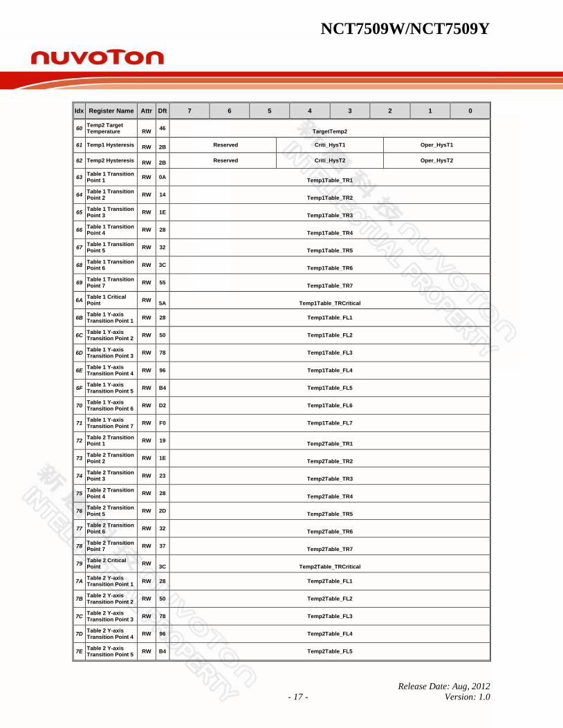
7. REGISTER SUMMARY
7.1 Register Map
Idx Register Name Attr Dft 7 6 5 4 3 2 1 0
0 LDT Readout RO 00 MNTREG_LT[7:0]
1 RT1 Temp MSB RO 00 MNTREG_RT1[10:3]
2 Alert Status RO 00 ADC_Busy STS_LTHA Reserved STS_RT1HA STS_RT1LA STS_RT1O STS_RT1C STS_TACH
3 Configuration [R] RW 15 ALERT_MSK STOP_Mnt DIS_FANOUT EN_FANIN Reserved EN_RT1 EN_WTC EN_FaultQue
ue
4 Conversion Rate [R]
RW 08 Reserved ConvRate[3:0]
5 LT Alert Temp [R] RW 46 LT_HAT[7:0]
6 Reserved Reserved
7 RT1 High Alert Temp MSB [R]
RW 46 RT1_HAT[10:3]
8 RT1 Low Alert Temp MSB [R]
RW D8 RT1_LAT[10:3]
9 Configuration [W] RW 15 ALERT_MSK STOP_Mnt DIS_FANOUT EN_FANIN Reserved EN_RT1 EN_WTC EN_FaultQue
ue
A Conversion Rate [W]
RW 08 Reserved ConvRate[3:0]
B LT Alert Temp [W] RW 46 LT_HAT[7:0]
C Reserved Reserved
D RT1 High Alert Temp MSB [W]
RW 46 RT1_HAT[10:3]
E RT1 Low Alert Temp MSB [W]
RW D8 RT1_LAT[10:3]
F One Shot Conversion
WO FF
10 RT1 Temp LSB RO 00 MNTREG_RT1[2:0] Reserved
11 RT1 Offset Temp MSB
RW 00 OFFSET_RT1[10:3]
12 RT1 Offset Temp LSB
RW 00 OFFSET_RT1[2:0] Reserved
13 RT1 High Alert Temp LSB
RW 00 RT1_HAT[2:0] Reserved
14 RT1 Low Alert Temp LSB
RW 00 RT1_LAT[2:0] Reserved
16 Alert Mask RW 06 MSK_LTH Reserved MSK_RT1H MSK_RT1L Reserved MSK_RT1C MSK_TACH
19 RT1 Critical Temp RW -- RT1_CT[7:0]
20 Reserved Reserved
21 Critical Temp Hysteresis
RW 0A Reserved CTH[4:0]
2D Customer Data Log Register 1
RW 00 CustomerLogReg1[7:0]
2E Customer Data Log Register 2
RW 00 CustomerLogReg2[7:0]
2F Customer Data Log Register 3
RW 00 CustomerLogReg3[7:0]
40 FAN Count Readout MSB
RO 00 FANIN[11:4]

NCT7509W/NCT7509Y
Release Date: Aug, 2012
- 16 - Version: 1.0
Idx Register Name Attr Dft 7 6 5 4 3 2 1 0
41 FAN Count Readout LSB
RO 00 FANIN[3:0] Reserved
42 FAN Count High Limit MSB
RW FF FANIN_HL[11:4]
43 FAN Count High Limit LSB
RW E0 FANIN_HL[3:0] Reserved
44 FanctrlDutyCycle RW 80 FANDuty
45 Configuration Register 1
RW 00 Share_Sour_Temp2 Share_Sour_Temp1
EN_ShareMode EN_SpeedCruise
46 Configuration Register 2
RW 10 Reserved Temp2FanSelect Temp1FanSelect FanControlMode
47 Configuration Register 3
RW A1 PWMPOL Reserved
Temp2_Sour_Sel Temp1_Sour_Sel
48 Configuration Register 4
RW 00 Reserved TwoDimension SimpleMode FastTracking
49 Dynamic feature Register 1
RW 50
Tcontrol
4A Dynamic feature Register 2
RW 3C
Tbound
4B Dynamic feature Register 3
RW 35 DownFan_Tol_FanDuty Weight_SYS Reserved
4C Dynamic feature Register 4
RW 52 Unstable_Depth StepCng_Up StepCng_Down
4D Dynamic feature Register 5
RW 02 FCount_FDuty_Weight_High (Twodimension = 1) FCount_FDuty_Step_High (Twodimension = 1)
4E Dynamic feature Register 6
RW 02 FCount_FDuty_Weight_Mid (Twodimension = 1) FCount_FDuty_Step_Mid (Twodimension = 1)
4F Dynamic feature Register 7
RW 04 FCount_FDuty_Weight_Low (Twodimension = 1) FCount_FDuty_Step_Low (Twodimension = 1)
50 Dynamic feature Register 8
RW 0A Generic_Tol_FanInCount
51 Dynamic feature Register 9
RW 99 RPM_Boundary_High[7:0]
52 Dynamic feature Register 10
RW 1C RPM_Boundary_Low[7:0]
53 Dynamic feature Register 11
RW 12 RPM_Boundary_High[11:8] RPM_Boundary_Low[11:8]
54 Dynamic feature Register 12
RW 05 DownFan_Tol_ FanInCount_High[7:0]
55 Dynamic feature Register 13
RW 0A DownFan_Tol_FanInCount_Low[7:0]
56 Fanctl Step Up Time RW 0A UpTime
57 Fanctl Step Down Time RW 0A DownTime
58 PWM1 Prescalar RW 84 CKSEL FanOutDivisor[6:0]
59 Fanctl Start Duty Cycle
RW 30 StartDutyCycle
5A Fanctl Nonstop Duty Cycle
RW 10 NonStopDutyCycle
5B Stop Time of Fanctl
RW FF StopTime
5C FANIN Target speed (HB)
RW 60 TargetFanInCount[11:4]
5D FANIN Target speed (LB)
RW 00 TargetFanInCount[3:0] Reserved
5E Target Speed Tolerance
RW 10 Reserved TOL_FanInCount[5:0]
5F Temp1 Target Temperature RW
46 TargetTemp1
NCT7509W/NCT7509Y
Release Date: Aug, 2012
- 17 - Version: 1.0
Idx Register Name Attr Dft 7 6 5 4 3 2 1 0
60 Temp2 Target Temperature RW
46 TargetTemp2
61 Temp1 Hysteresis RW 2B Reserved Criti_HysT1 Oper_HysT1
62 Temp2 Hysteresis RW 2B Reserved Criti_HysT2 Oper_HysT2
63 Table 1 Transition Point 1
RW 0A Temp1Table_TR1
64 Table 1 Transition Point 2
RW 14 Temp1Table_TR2
65 Table 1 Transition Point 3
RW 1E Temp1Table_TR3
66 Table 1 Transition Point 4
RW 28 Temp1Table_TR4
67 Table 1 Transition Point 5
RW 32 Temp1Table_TR5
68 Table 1 Transition Point 6
RW 3C Temp1Table_TR6
69 Table 1 Transition Point 7
RW 55 Temp1Table_TR7
6A Table 1 Critical Point
RW 5A Temp1Table_TRCritical
6B Table 1 Y-axis Transition Point 1
RW 28 Temp1Table_FL1
6C Table 1 Y-axis Transition Point 2
RW 50 Temp1Table_FL2
6D Table 1 Y-axis Transition Point 3
RW 78 Temp1Table_FL3
6E Table 1 Y-axis Transition Point 4
RW 96 Temp1Table_FL4
6F Table 1 Y-axis Transition Point 5
RW B4 Temp1Table_FL5
70 Table 1 Y-axis Transition Point 6
RW D2 Temp1Table_FL6
71 Table 1 Y-axis Transition Point 7
RW F0 Temp1Table_FL7
72 Table 2 Transition Point 1
RW 19 Temp2Table_TR1
73 Table 2 Transition Point 2
RW 1E Temp2Table_TR2
74 Table 2 Transition Point 3
RW 23 Temp2Table_TR3
75 Table 2 Transition Point 4
RW 28 Temp2Table_TR4
76 Table 2 Transition Point 5
RW 2D Temp2Table_TR5
77 Table 2 Transition Point 6
RW 32 Temp2Table_TR6
78 Table 2 Transition Point 7
RW 37 Temp2Table_TR7
79 Table 2 Critical Point
RW 3C Temp2Table_TRCritical
7A Table 2 Y-axis Transition Point 1
RW 28 Temp2Table_FL1
7B Table 2 Y-axis Transition Point 2
RW 50 Temp2Table_FL2
7C Table 2 Y-axis Transition Point 3
RW 78 Temp2Table_FL3
7D Table 2 Y-axis Transition Point 4
RW 96 Temp2Table_FL4
7E Table 2 Y-axis Transition Point 5
RW B4 Temp2Table_FL5

NCT7509W/NCT7509Y
Release Date: Aug, 2012
- 18 - Version: 1.0
Idx Register Name Attr Dft 7 6 5 4 3 2 1 0
7F Table 2 Y-axis Transition Point 6
RW D2 Temp2Table_FL6
80 Table 2 Y-axis Transition Point 7
RW F0 Temp2Table_FL7
BF RT Filter & Alert mode
RW 00 Reserved RT1F Alert_MD
FD CID (Chip ID) RO 50 50h
FE VID (Vendor ID) RO 50 50h
FF DID (Device ID) RO 9x 9xH (x=0,1,2…)
7.2 Register Detail
7.2.1 Local Diode Temperature Readout Register
Location : Address 00h
Type : Read Only
Power on default value : 00
BIT 7 6 5 4 3 2 1 0
Name Local Diode Temperature Readout Value. The real temperature value calculation is referred to TEMPERATURE MEASUREMENT DATA FORMAT.
Value SIGN 64 32 16 8 4 2 1
7.2.2 Remote Diode 1 Temperature Readout (MSB) Register
Location : Address 01h
Type : Read Only
Power on default value : 00
BIT 7 6 5 4 3 2 1 0
Name Remote Diode 1 Temperature Readout Value. The real temperature value calculation is referred to TEMPERATURE MEASUREMENT DATA FORMAT.
Value SIGN 64 32 16 8 4 2 1
7.2.3 Alert Status Register
Location : Address 02h
Type : Read Only
Power on default value : 00
BIT 7 6 5 4 3 2 1 0
Name ADC_Busy STS_LTHA Reserved STS_RT1HA STS_RT1LA STS_RT1O STS_RT1C STS_TACH
Default 0 0 0 0 0 0 0
BIT FLAG NAME DESCRIPTION

NCT7509W/NCT7509Y
Release Date: Aug, 2012
- 19 - Version: 1.0
BIT FLAG NAME DESCRIPTION
7 ADC_Busy If set to ‘1’ indicates ADC is busy converting.
6 STS_LTHA If set to ‘1’ indicates a measured Local Diode Temperature Higher than Local High set point (High Limit).
5 Reserved
4 STS_RT1HA If set to ‘1’ indicates a measured Remote Diode1 Temperature higher than Remote High set point (High Limit).
3 STS_RT1LA If set to ‘1’ indicates a measured Remote Diode1 Temperature lower than Remote Low set point (Low Limit).
2 STS_RT1O If set to ‘1’ indicates a Remote Diode1 disconnect.
1 STS_RT1C If set to ‘1’ indicates a Remote Diode1 Critical Temperature alarm.
0 STS_TACH If set to ‘1’ indicates Tachometer count is higher than Tachometer Limit.
7.2.4 Configuration Register
Location : Address 03h and 09h
Type : Read/Write
Power on default value : 15
BIT 7 6 5 4 3 2 1 0
Name ALERT_
MSK STOP_
Mnt DIS_FANOUT
EN_FANIN
RESERVED
EN_RT1 EN_WT
C EN_FaultQueue
Default 0 0 0 1 1 0 1
BIT DESCRIPTION
7
ALERT_MSK – ALERT# function is enable
0 = Enable
1 = Disable
6
STOP_Mnt – Stop Monitor and entry Standby
0 = Monitor
1 = Stop Monitor
5
DIS_FANOUT– Disable PWM FANOUT.
0 = Enable PWM FANOUT
1 = Disable PWM FANOUT
4
EN_FANIN– Enable FANIN monitoring.
0 = Disable
1 = Enable
2 EN_RT1 – Enable Remote Diode 1 monitoring.
0 = Disable
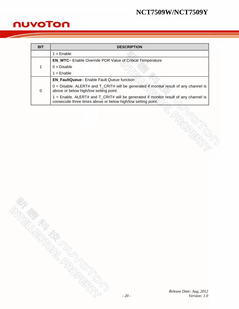
NCT7509W/NCT7509Y
Release Date: Aug, 2012
- 20 - Version: 1.0
BIT DESCRIPTION
1 = Enable
1
EN_WTC– Enable Override POR Value of Critical Temperature
0 = Disable
1 = Enable
0
EN_FaultQueue– Enable Fault Queue function
0 = Disable. ALERT# and T_CRIT# will be generated if monitor result of any channel is above or below high/low setting point.
1 = Enable. ALERT# and T_CRIT# will be generated if monitor result of any channel is consecuite three times above or below high/low setting point.

NCT7509W/NCT7509Y
Release Date: Aug, 2012
- 21 - Version: 1.0
7.2.5 Conversion Rate Register
Location : Address 04h and 0Ah
Type : Read/Write
Power on default value : 08
BIT 7 6 5 4 3 2 1 0
Name Reserved ConvRate
Default 1 0 0 0
BIT<D7:D0> FREQUENCY/TIME
00h 0.0625Hz / 16sec
01h 0.125Hz / 8sec
02h 0.25Hz / 4sec
03h 0.5Hz / 2sec
04h 1Hz / 1sec
05h 2Hz / 0.5sec
06h 4Hz / 0.25sec
07h 8Hz / 0.125sec
08h 16Hz / 0.0625sec
09h-FFh Reserved
7.2.6 Local Diode Temperature Alert Temperature Register
Location : Address 05h and 0Bh
Type : Read/Write
Power on default value : 46
BIT 7 6 5 4 3 2 1 0
Name LDT Alert Temperature
Value SIGN 64 32 16 8 4 2 1
Default 46HEX (70℃)
7.2.7 Remote Diode 1 Temperature High Alert Temperature (MSB) Register
Location : Address 07h and 0Dh
Type : Read/Write
Power on default value : 46
BIT 7 6 5 4 3 2 1 0
Name RT1 High Alert Temperature High Byte
Value SIGN 64 32 16 8 4 2 1

NCT7509W/NCT7509Y
Release Date: Aug, 2012
- 22 - Version: 1.0
Default 46HEX (70℃)
7.2.8 Remote Diode 1 Temperature Low Alert Temperature (MSB) Register
Location : Address 08h and 0Eh
Type : Read/Write
Power on default value : D8
BIT 7 6 5 4 3 2 1 0
Name RT1 Low Alert Temperature High Byte
Value SIGN 64 32 16 8 4 2 1
Default D8HEX (-40℃)
7.2.9 One Shot Conversion Register
Location : Address 0Fh
Type : Write Only
BIT DESCRIPTION
7-0 One Shot Conversion – When enter Stop Monitor state, to fill any value into this register will trigger one temperature conversion cycle.
7.2.10 Remote Diode 1 Temperature Readout (LSB) Register
Location : Address 10h
Type : Read Only
Power on default value : 00
BIT 7 6 5 4 3 2 1 0
Name Remote Diode 1 Temperature Readout Value. The
real temperature value calculation is referred to TEMPERATURE MEASUREMENT DATA FORMAT.
Reserved
Value 0.5 0.25 0.125 0
7.2.11 Remote Diode 1 Temperature Offset Register (MSB) Register
Location : Address 11h
Type : Read/Write
Power on default value : 00
BIT 7 6 5 4 3 2 1 0
Name RT1 OFFSET VALEU High Byte
Value SIGN 64 32 16 8 4 2 1
Default 00HEX
NCT7509W/NCT7509Y
Release Date: Aug, 2012
- 23 - Version: 1.0
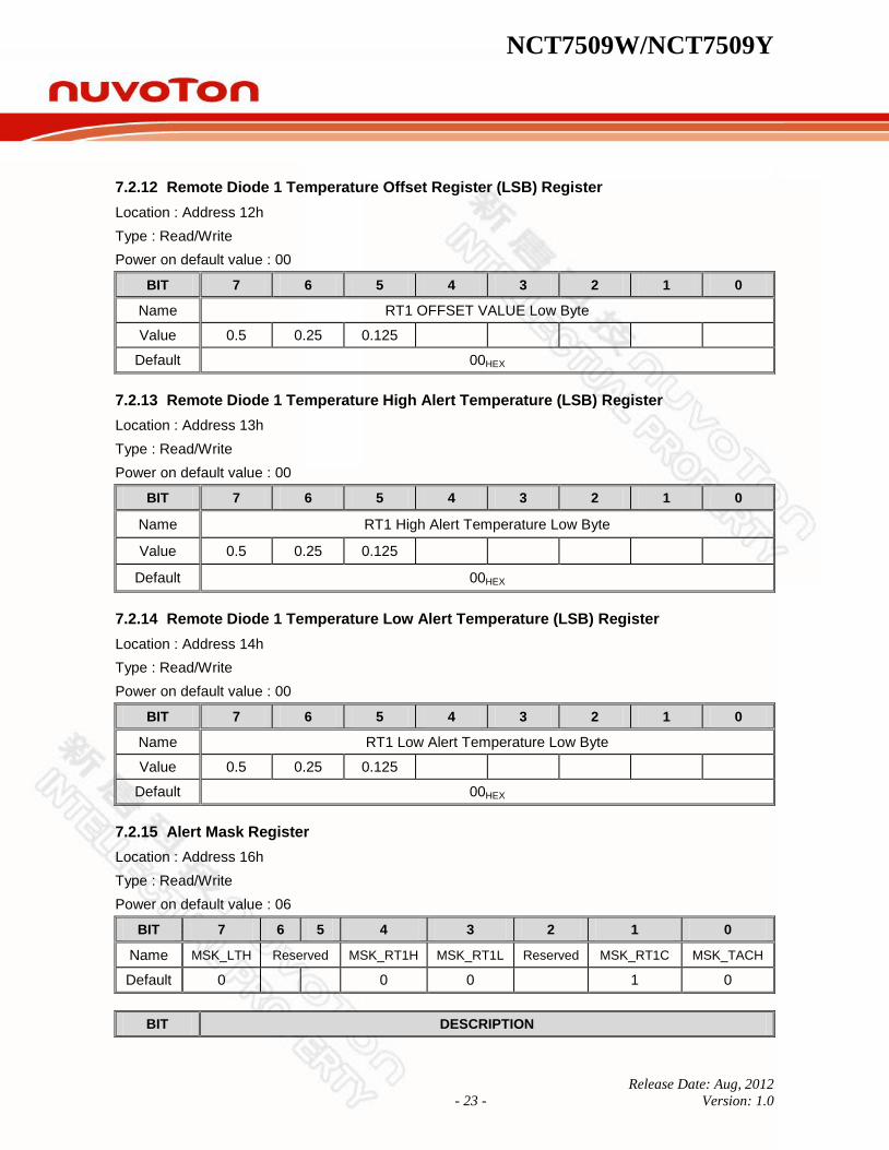
7.2.12 Remote Diode 1 Temperature Offset Register (LSB) Register
Location : Address 12h
Type : Read/Write
Power on default value : 00
BIT 7 6 5 4 3 2 1 0
Name RT1 OFFSET VALUE Low Byte
Value 0.5 0.25 0.125
Default 00HEX
7.2.13 Remote Diode 1 Temperature High Alert Temperature (LSB) Register
Location : Address 13h
Type : Read/Write
Power on default value : 00
BIT 7 6 5 4 3 2 1 0
Name RT1 High Alert Temperature Low Byte
Value 0.5 0.25 0.125
Default 00HEX
7.2.14 Remote Diode 1 Temperature Low Alert Temperature (LSB) Register
Location : Address 14h
Type : Read/Write
Power on default value : 00
BIT 7 6 5 4 3 2 1 0
Name RT1 Low Alert Temperature Low Byte
Value 0.5 0.25 0.125
Default 00HEX
7.2.15 Alert Mask Register
Location : Address 16h
Type : Read/Write
Power on default value : 06
BIT 7 6 5 4 3 2 1 0
Name MSK_LTH Reserved MSK_RT1H MSK_RT1L Reserved MSK_RT1C MSK_TACH
Default 0 0 0 1 0
BIT DESCRIPTION

NCT7509W/NCT7509Y
Release Date: Aug, 2012
- 24 - Version: 1.0
BIT DESCRIPTION
7
MSK_LTH – Local Diode Temperature High Alert Mask
0 = Alert is not masked
1 = Alert is masked
4
MSK_RT1H– Remote Diode 1 Temperature High Alert Mask
0 = Alert is not masked
1 = Alert is masked
3
MSK_RT1L– Remote Diode 1 Temperature Low Alert Mask
0 = Alert is not masked
1 = Alert is masked
1
MSK_RT1C– Remote Diode 1 Temperature Critical Mask
0 = Alert is not masked
1 = Alert is masked
0
MSK_TACH– Fan Tachometer Alert Mask
0 = Alert is not masked
1 = Alert is masked
7.2.16 Remote Diode 1 Critical Temperature Register
Location : Address 19h
Type : Read/Write
Power on default value : Power on trapping after power up 100ms
BIT 7 6 5 4 3 2 1 0
Name RT1 Critical Temperature
The format of Temperature is 8-bit 2’s complement and the range is –128℃~127℃.
Value SIGN 64 32 16 8 4 2 1
Default Hardware Strapping
The default value is trapping after power up 100ms by different pull-up resistors of ALERT# pin :
PULL-UP RESISTOR TEMPERATURE (℃)
ALERT#
2KΩ 75
7.5KΩ 90
10.5KΩ 100
14KΩ 105
18.7KΩ 110

NCT7509W/NCT7509Y
Release Date: Aug, 2012
- 25 - Version: 1.0
7.2.17 Critical Temperature Hysteresis Register
Location : Address 21h
Type : Read/Write
Power on default value : 0A
BIT 7 6 5 4 3 2 1 0
Name Critical Temperature Hysteresis
The format of Temperature is 5-bit integer and the range is 0℃~31℃.
Value 16 8 4 2 1
Default 0AHEX (10℃)
7.2.18 Customer Data Log Registers
Location : Address 2Dh 2Eh 2Fh
Type : Read/Write
Power on default value : 00
BIT 7 6 5 4 3 2 1 0
Name Customer Data Log Register
Default 00HEX
7.2.19 Fan Count Readout (MSB) Register
Location : Address 40h
Type : Read Only
Power on default value : 00
BIT 7 6 5 4 3 2 1 0
Name
FANIN tachometer readout high byte. The real FANIN RPM value calculation is referred to FANIN COUNT CACLULATION description.
12-bitCount Value bit[11:4]
7.2.20 Fan Count Readout (LSB) Register
Location : Address 41h
Type : Read Only
Power on default value : 00
BIT 7 6 5 4 3 2 1 0
Name FANIN tachometer readout low byte
12-bitCount Value bit [3:0] Reserved.

NCT7509W/NCT7509Y
Release Date: Aug, 2012
- 26 - Version: 1.0
7.2.21 Fan Count High Limit (MSB) Register
Location : Address 42h
Type : Read/Write
Power on default value : FF
BIT 7 6 5 4 3 2 1 0
Name
FANIN_HL
FANIN tachometer count limit (high byte). The real FANIN RPM count limit value calculation is referred to FANIN COUNT CACLULATION description.
12-bitCount Value bit[11:4]
Default FFHEX
7.2.22 Fan Count High Limit (LSB) Register
Location : Address 43h
Type : Read/Write
Power on default value : EE
BIT 7 6 5 4 3 2 1 0
Name
FANIN_HL_LSB Reversed
FANIN tachometer count limit (lowe byte).
12-bitCount Value bit [3:0]
Default EEHEX
7.2.23 Fanctrl Duty Cycle Register
Location : Address 44h
Type : Read / Write (in Manual Mode)
Read Only (in the Smart Fan mode)
Power on default value : 80
BIT 7 6 5 4 3 2 1 0
Name FANDuty
Default 80HEX
BIT DESCRIPTION
7-0
FANDuty – Current Fanctrl output value.
In Manual Mode, programming this register to set desired PWM duty cycle.
In Thermal Cruise or SMART FANTM
IV algorithm, this register reveals the current PWM duty cycle and is Read Only.

NCT7509W/NCT7509Y
Release Date: Aug, 2012
- 27 - Version: 1.0
7.2.24 Generic Fan Control Configuration Register 1 (GFCCR1) Register
Location : Address 45h
Type : Read/Write
Power on default value : 00
BIT 7 6 5 4 3 2 1 0
Name Share_Sour_Temp2 Share_Sour_Temp1 EN_ShareMode EN_SpeedCruise
Default 00HEX
BIT DESCRIPTION
7-5
Share_Sour_Temp2 : Select which temperature source could share control table in SMART FAN
TM IV mode
001 : Local temperature will be referred to SMART FANTM
IV control table 2
010 : Remote 1 temperature will be referred to SMART FANTM
IV control table 2
Others : Reserved
4-2
Share_Sour_Temp1 : Select which temperature source could share control table in SMART FAN
TM IV mode
001 : Local temperature will be referred to SMART FANTM
IV control table 1
010 : Remote 1 temperature will be referred to SMART FANTM
IV control table 1
Others : Reserved
1
EN_ShareMode : Enable sharing table function in SMART FANTM
IV control mode
0 = Disable
1 = Enable
0
EN_SpeedCruise : Apply Speed CruiseTM
mode to FANCTL
0 = Fan control mode is decide by GFCCR2 register. (Default)
1 = FANCTL is applies to Speed CruiseTM
control for FANIN speed input.
7.2.25 Generic Fan Control Configuration Register 2 (GFCCR2) Register
Location : Address 46h
Type : Read/Write
Power on default value : 10
BIT 7 6 5 4 3 2 1 0
Name Reserved Temp2FanSelect Temp1FanSelect FanControlMode
Default 10HEX
BIT DESCRIPTION

NCT7509W/NCT7509Y
Release Date: Aug, 2012
- 28 - Version: 1.0
BIT DESCRIPTION
7-4 Reserved.
3
Temp2 FanSelect : Decide temp2 whether effect FANCTRL or not.
0 = Independent
1 = Dependent
2
Temp1 FanSelect : Decide temp1 whether effect FANCTRL or not.
0 = Independent
1 = Dependent
1-0
FanControlMode : From temperature view, decide Fan Control mode
00 : Temp2 & Temp1 practice thermal cruise algorithm
01: Temp2 practices thermal cruise algorithm and Temp1 is SMART FANTM
IV algorithm
Others : Reserved
7.2.26 Generic Fan Control Configuration Register 3 (GFCCR3) Register
Location : Address 47h
Type : Read/Write
Power on default value : A1
BIT 7 6 5 4 3 2 1 0
Name PWMPOL Reserved Temp2_Sour_Sel Temp1_Sour_Sel
Default A1HEX
BIT DESCRIPTION
7
PWMPOL : Control FANCTL PWM output polarity.
0 = Low active. PWM is controlled by negative duty cycle.
1 = High active. (Default). PWM is controlled by positive duty cycle.
6 Reserved
5-3
Temp2_Sour_Sel : Temperature source selection for Table2 in SMART FANTM
IV algorithm
001 = Local temperature
010 = Remote temperature 1
Others : Reserved
2-0
Temp1_Sour_Sel : Temperature source selection for Table1 in SMART FANTM
IV algorithm
001 = Local temperature
010 = Remote temperature 1
Others : Reserved
NCT7509W/NCT7509Y
Release Date: Aug, 2012
- 29 - Version: 1.0
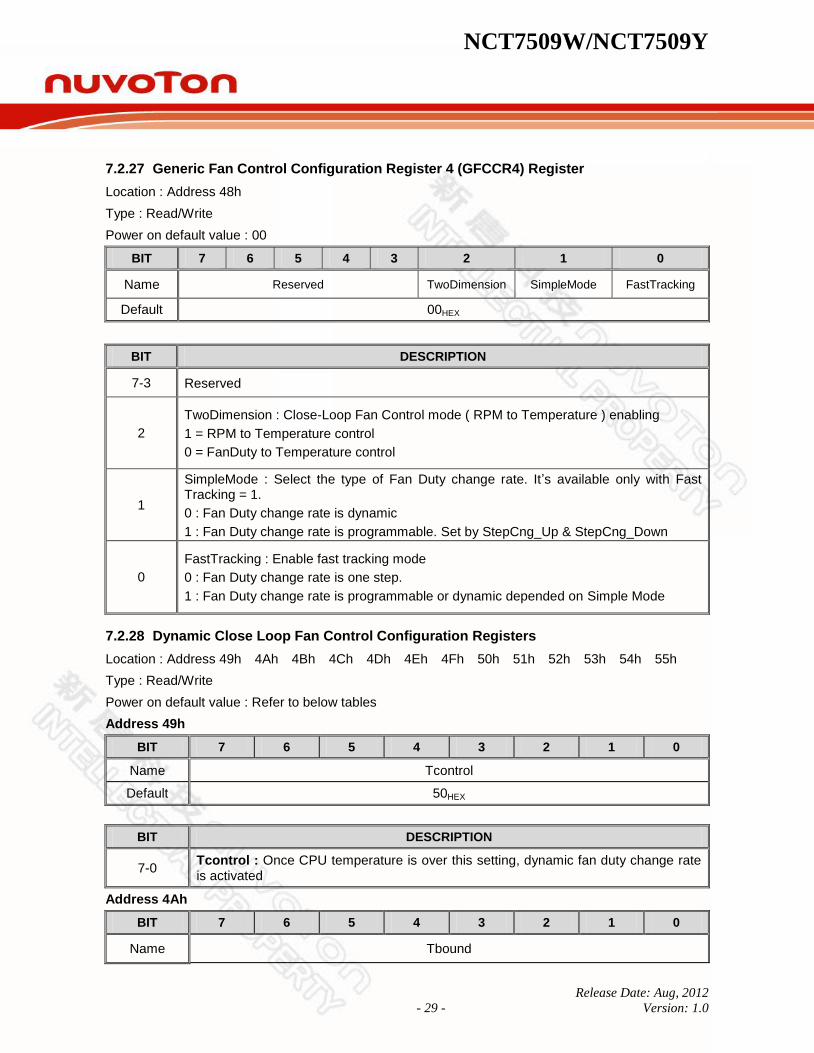
7.2.27 Generic Fan Control Configuration Register 4 (GFCCR4) Register
Location : Address 48h
Type : Read/Write
Power on default value : 00
BIT 7 6 5 4 3 2 1 0
Name Reserved TwoDimension SimpleMode FastTracking
Default 00HEX
BIT DESCRIPTION
7-3 Reserved
2
TwoDimension : Close-Loop Fan Control mode ( RPM to Temperature ) enabling
1 = RPM to Temperature control
0 = FanDuty to Temperature control
1
SimpleMode : Select the type of Fan Duty change rate. It’s available only with Fast Tracking = 1.
0 : Fan Duty change rate is dynamic
1 : Fan Duty change rate is programmable. Set by StepCng_Up & StepCng_Down
0
FastTracking : Enable fast tracking mode
0 : Fan Duty change rate is one step.
1 : Fan Duty change rate is programmable or dynamic depended on Simple Mode
7.2.28 Dynamic Close Loop Fan Control Configuration Registers
Location : Address 49h 4Ah 4Bh 4Ch 4Dh 4Eh 4Fh 50h 51h 52h 53h 54h 55h
Type : Read/Write
Power on default value : Refer to below tables
Address 49h
BIT 7 6 5 4 3 2 1 0
Name Tcontrol
Default 50HEX
BIT DESCRIPTION
7-0 Tcontrol : Once CPU temperature is over this setting, dynamic fan duty change rate is activated
Address 4Ah
BIT 7 6 5 4 3 2 1 0
Name Tbound

NCT7509W/NCT7509Y
Release Date: Aug, 2012
- 30 - Version: 1.0
Default 3CHEX
BIT DESCRIPTION
7-0 Tbound : Once System temperature is over this setting, dynamic fan duty change rate is activated
Address 4Bh
BIT 7 6 5 4 3 2 1 0
Name DownFan_Tol_FanDuty Weight_SYS Reserved
Default 35HEX
BIT DESCRIPTION
7 - 4
DownFan_Tol_FanDuty : Tracking tolerance of FanDuty while FanDuty is decreasing
1111 : 15 / .... / 0000 : 0
Ex : Setting 3 => Final FanDuty = (Target FanDuty + 3) while FanDuty is descending.
3 – 2
Weight_STS : Multiplication factor of System fan; the tracking speed of CPU fan responds to this setting.
00 : 0.25 01 : 0.5 10 : 1 11 : 2
1 - 0 Reserved
Address 4Ch
BIT 7 6 5 4 3 2 1 0
Name Reserved StepCng_Up StepCng_Down
Default 52HEX
BIT DESCRIPTION
7 - 6 Reserved
5 - 3 StepCng_Up : Fixed increasing step of fan duty; only available with Simple Mode = 1
2 - 0 StepCng_Down : Fixed decreasing step of fan duty; only available with Simple Mode = 1
NCT7509W/NCT7509Y
Release Date: Aug, 2012
- 31 - Version: 1.0
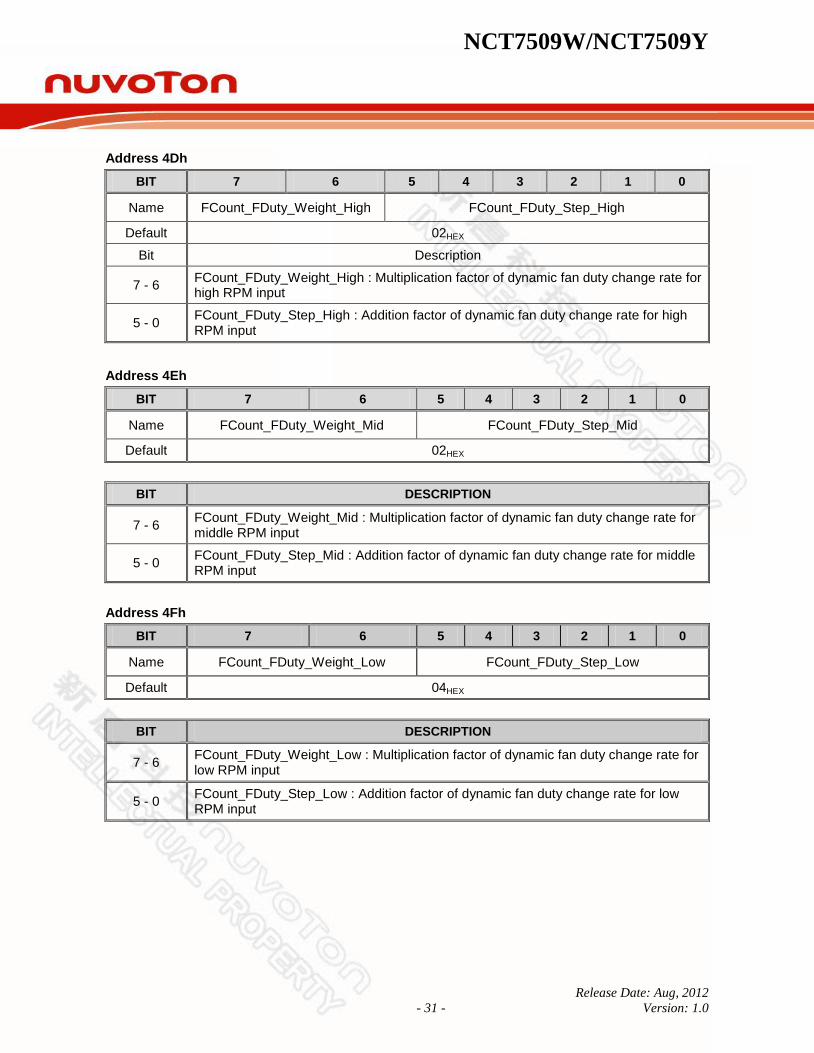
Address 4Dh
BIT 7 6 5 4 3 2 1 0
Name FCount_FDuty_Weight_High FCount_FDuty_Step_High
Default 02HEX
Bit Description
7 - 6 FCount_FDuty_Weight_High : Multiplication factor of dynamic fan duty change rate for high RPM input
5 - 0 FCount_FDuty_Step_High : Addition factor of dynamic fan duty change rate for high RPM input
Address 4Eh
BIT 7 6 5 4 3 2 1 0
Name FCount_FDuty_Weight_Mid FCount_FDuty_Step_Mid
Default 02HEX
BIT DESCRIPTION
7 - 6 FCount_FDuty_Weight_Mid : Multiplication factor of dynamic fan duty change rate for middle RPM input
5 - 0 FCount_FDuty_Step_Mid : Addition factor of dynamic fan duty change rate for middle RPM input
Address 4Fh
BIT 7 6 5 4 3 2 1 0
Name FCount_FDuty_Weight_Low FCount_FDuty_Step_Low
Default 04HEX
BIT DESCRIPTION
7 - 6 FCount_FDuty_Weight_Low : Multiplication factor of dynamic fan duty change rate for low RPM input
5 - 0 FCount_FDuty_Step_Low : Addition factor of dynamic fan duty change rate for low RPM input

NCT7509W/NCT7509Y
Release Date: Aug, 2012
- 32 - Version: 1.0
Address 50h
BIT 7 6 5 4 3 2 1 0
Name Generic_Tol_FanInCount
Default 0AHEX
BIT DESCRIPTION
7 - 0
Generic_Tol_FanInCount : Tracking tolerance of input Fan Count under Two Dimension = 1
Ex : Setting 3 =>
If current FANIN count = (Target FANIN count - 3) ~ (Target FANIN count + 3) then FanDuty will be maintained
Address 51h
BIT 7 6 5 4 3 2 1 0
Name RPM_Boundary_High[7:0]
Default 99HEX
BIT DESCRIPTION
7 - 0
RPM_Boundary_High[7:0] : Low byte of high RPM speed boundary setting. It must be fan count format
Ex : Fan Count = 1350,000 / RPM
Address 52h
BIT 7 6 5 4 3 2 1 0
Name RPM_Boundary_Low[7:0]
Default 1CHEX
BIT DESCRIPTION
7 - 0
RPM_Boundary_Low[7:0] : Low byte of low RPM speed boundary setting. It must be fan count format
Ex : Fan Count = 1350,000 / RPM
Address 53h
BIT 7 6 5 4 3 2 1 0
Name RPM_Boundary_High[11:8] RPM_Boundary_Low[11:8]
Default 12HEX
BIT DESCRIPTION
7 - 0 RPM_Boundary_High[11:8] : High byte of high RPM speed boundary setting. It must be fan count format

NCT7509W/NCT7509Y
Release Date: Aug, 2012
- 33 - Version: 1.0
RPM_Boundary_Low[11:8] : High byte of low RPM speed boundary setting. It must be fan count format
Ex : Fan Count = 1350,000 / RPM
Address 54h
BIT 7 6 5 4 3 2 1 0
Name DownFan_Tol_FanInCount_High
Default 05HEX
BIT DESCRIPTION
7 - 0
DownFan_Tol_FanInCount_High : Tracking tolerance of input Fan Count under high RPM speed with
Two Dimension = 1 & Fast Tracking = 1
Ex : Setting 3 =>
If the current FANIN count reaches (Target FANIN count - 3) then tracking stops
Address 55h
BIT 7 6 5 4 3 2 1 0
Name DownFan_Tol_FanInCount_Low
Default 0AHEX
BIT DESCRIPTION
7 - 0
DownFan_Tol_FanInCount_Low : Tracking tolerance of input Fan Count under low RPM speed with
Two Dimension = 1 & Fast Tracking = 1
Ex : Setting 3 =>
If the current FANIN count reaches (Target FANIN count - 3) then tracking stops
7.2.29 SMART FANTM
IV Control Output Step Up Time Register
Location : Address 56h
Type : Read/Write
Power on default value : 0A
BIT 7 6 5 4 3 2 1 0
Name UpTime (Smart Fan Step Up Time). Unit in 0.1sec. Programmed as the interval of continuous Fan ramping up.
Default 0AHEX
This register should not be set to 0. Otherwise, the fan duty will be abnormal.

NCT7509W/NCT7509Y
Release Date: Aug, 2012
- 34 - Version: 1.0
7.2.30 SMART FANTM
IV Control Output Step Down Time Register
Location : Address 57h
Type : Read/Write
Power on default value : 0A
BIT 7 6 5 4 3 2 1 0
Name DownTime (Smart Fan Step Down Time). Unit in 0.1sec. Programmed as the interval of continuous Fan ramping Down.
Default 0AHEX
This register should not be set to 0. Otherwise, the fan duty will be abnormal.
7.2.31 Fan Output PWM Frequency Prescalar Register
Location : Address 58h
Type : Read/Write
Power on default value : 84
BIT 7 6 5 4 3 2 1 0
Name CKSEL FanOutDivisor
Default 1 0 0 0 0 1 0 0
A wide range of clocks can be selected to satisfy customer needs. The default output frequency is around 25 KHz.
BIT DESCRIPTION
7
CLKSEL BASE Frequency
0 1.024KHz
1 125KHz
6-0 Divisor – Clock frequency Divisor.
There are 2 divisors depending on CKSEL :
If CKSEL equals 1, then the output clock is simply equal to 125/ (Divisor+1) KHz .
If CKSEL equals 0, the output clock is 1.024KHz/MappedDivisor.
MappedDivisor depends on Divisor[3:0] and is described in the table below.
DIVISOR[3:0] MAPPED DIVISOR
OUTPUT FREQUENCY
DIVISOR[3:0] MAPPED DIVISOR
OUTPUT FREQUENCY
0000 1 1024Hz 1000 12 85Hz
0001 2 512Hz 1001 16 64Hz
0010 3 341Hz 1010 32 32Hz
0011 4 256Hz 1011 64 16Hz
0100 5 205Hz 1100 128 8Hz
0101 6 171Hz 1101 256 4Hz

NCT7509W/NCT7509Y
Release Date: Aug, 2012
- 35 - Version: 1.0
DIVISOR[3:0] MAPPED DIVISOR
OUTPUT FREQUENCY
DIVISOR[3:0] MAPPED DIVISOR
OUTPUT FREQUENCY
0110 7 146Hz 1110 512 2Hz
0111 8 128Hz 1111 1024 1Hz
7.2.32 Fan Output Start-up Value Register
Location : Address 59h
Type : Read/Write
Power on default value : 30
BIT 7 6 5 4 3 2 1 0
Name FanStartDuty
Default 30HEX
BIT DESCRIPTION
7-0 FanStartDuty –control the FANCTL fan output start-up value.
7.2.33 Fan Output Nonstop Value Register
Location : Address 5Ah
Type : Read/Write
Power on default value : 10
BIT 7 6 5 4 3 2 1 0
Name FanNonStop
Default 10HEX
BIT DESCRIPTION
7-0 FanNonStop – control the FANCTL fan output nonstop value.
7.2.34 Fan Output Stop Time Register
Location : Address 5Bh
Type : Read/Write
Power on default value : FF
BIT 7 6 5 4 3 2 1 0
Name FanStopTime
Default FFHEX
BIT DESCRIPTION

NCT7509W/NCT7509Y
Release Date: Aug, 2012
- 36 - Version: 1.0
7-0
FanStopTime – control the FANCTL fan stop time from Fan Output Nonstop Value to the off state.
Unit in 0.1sec. Ranges from 0.1sec to 25.5sec.
If set to 0, the fan will never stop.

NCT7509W/NCT7509Y
Release Date: Aug, 2012
- 37 - Version: 1.0
7.2.35 FANIN Target Speed Register
Location : Address 5Ch 5Dh
Type : Read/Write
Power on default value : Refer to below tables
FANIN Target Speed High Byte
BIT 7 6 5 4 3 2 1 0
Name
FTSH : FANIN tachometer target speed high byte.
The real FANIN RPM value calculation is referred to FANIN COUNT CACLULATION description.
12-bitCount Value bit[11:4]
Default 60HEX
FANIN Target Speed Low Byte
BIT 7 6 5 4 3 2 1 0
Name FTSL: FANIN tachometer target speed low byte.
12-bitCount Value bit [3:0] Reserved.
Default 00HEX
In Fan Speed CruiseTM
mode, each FANIN tachometer has to have a target fan speed. The NCT7509 will try to tune relative fan output to keep the fan speed of target. The default target speed for FANIN tachometer is 6000HEX .
7.2.36 Tolerance of FANIN Target Speed Register
Location : Address 5Eh
Type : Read/Write
Power on default value : 10
BIT 7 6 5 4 3 2 1 0
Name Reserved Tolerance of FANIN Target Speed
Default 0 0 0 1 0 0 0 0
BIT DESCRIPTION
7-6 Reserved.
5-0 Tolerance of FANIN Target Speed
Tolerance of FANIN tachometer target speed. Tolerance range is 00h~3Fh
NCT7509W/NCT7509Y
Release Date: Aug, 2012
- 38 - Version: 1.0
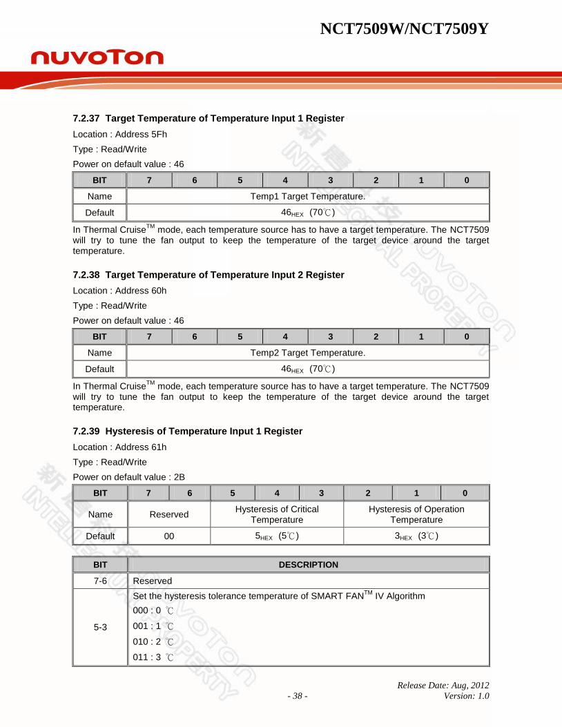
7.2.37 Target Temperature of Temperature Input 1 Register
Location : Address 5Fh
Type : Read/Write
Power on default value : 46
BIT 7 6 5 4 3 2 1 0
Name Temp1 Target Temperature.
Default 46HEX (70℃)
In Thermal CruiseTM
mode, each temperature source has to have a target temperature. The NCT7509 will try to tune the fan output to keep the temperature of the target device around the target temperature.
7.2.38 Target Temperature of Temperature Input 2 Register
Location : Address 60h
Type : Read/Write
Power on default value : 46
BIT 7 6 5 4 3 2 1 0
Name Temp2 Target Temperature.
Default 46HEX (70℃)
In Thermal CruiseTM
mode, each temperature source has to have a target temperature. The NCT7509 will try to tune the fan output to keep the temperature of the target device around the target temperature.
7.2.39 Hysteresis of Temperature Input 1 Register
Location : Address 61h
Type : Read/Write
Power on default value : 2B
BIT 7 6 5 4 3 2 1 0
Name Reserved Hysteresis of Critical
Temperature Hysteresis of Operation
Temperature
Default 00 5HEX (5℃) 3HEX (3℃)
BIT DESCRIPTION
7-6 Reserved
5-3
Set the hysteresis tolerance temperature of SMART FANTM
IV Algorithm
000 : 0 ℃
001 : 1 ℃
010 : 2 ℃
011 : 3 ℃
NCT7509W/NCT7509Y
Release Date: Aug, 2012
- 39 - Version: 1.0
BIT DESCRIPTION
....
111 : 7 ℃
2-0
Set the hysteresis tolerance temperature of SMART FANTM
IV Algorithm
000 : 0 ℃
001 : 1 ℃
010 : 2 ℃
011 : 3 ℃
....
111 : 7 ℃
In Thermal Cruise and SMART FANTM
IV mode, to prevent unstable temperatures from throttling the fan speed, the NCT7509 employs a hysteresis temperature to separate the speed-up/slow-down temperature points.
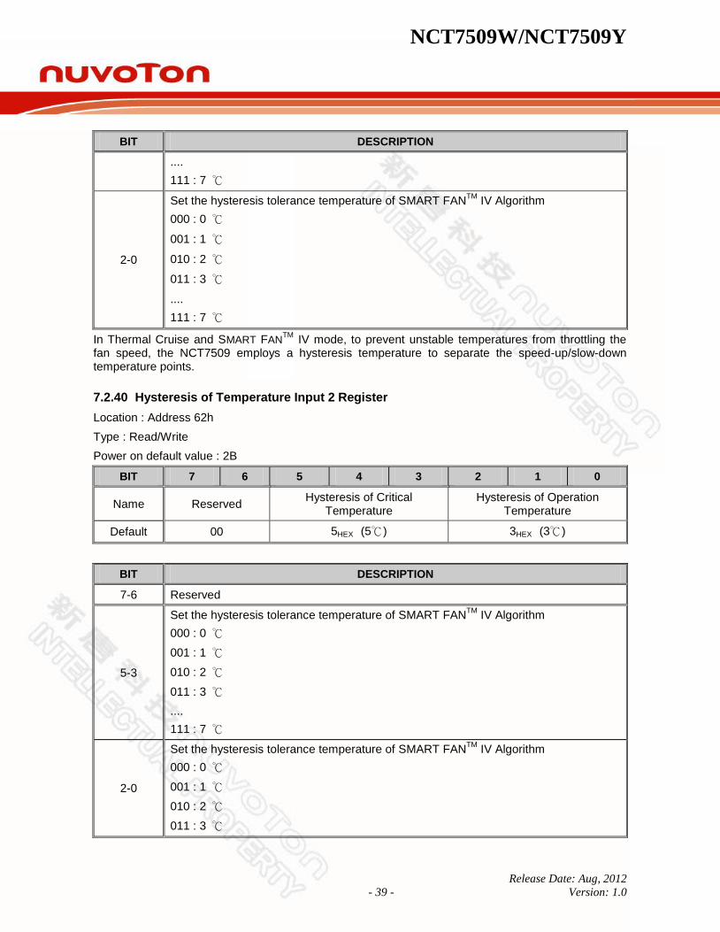
7.2.40 Hysteresis of Temperature Input 2 Register
Location : Address 62h
Type : Read/Write
Power on default value : 2B
BIT 7 6 5 4 3 2 1 0
Name Reserved Hysteresis of Critical
Temperature Hysteresis of Operation
Temperature
Default 00 5HEX (5℃) 3HEX (3℃)
BIT DESCRIPTION
7-6 Reserved
5-3
Set the hysteresis tolerance temperature of SMART FANTM
IV Algorithm
000 : 0 ℃
001 : 1 ℃
010 : 2 ℃
011 : 3 ℃
....
111 : 7 ℃
2-0
Set the hysteresis tolerance temperature of SMART FANTM
IV Algorithm
000 : 0 ℃
001 : 1 ℃
010 : 2 ℃
011 : 3 ℃

NCT7509W/NCT7509Y
Release Date: Aug, 2012
- 40 - Version: 1.0
....
111 : 7 ℃
In Thermal Cruise and SMART FANTM
IV mode, to prevent unstable temperatures from throttling the fan speed, the NCT7509 employs a hysteresis temperature to separate the speed-up/slow-down temperature points.
7.2.41 SMART FANTM
IV Temperature and PWM Registers Register
Location : Address 63h ~ 80h
Type : Read/Write
Power on default value: Refer to below tables
SMART FANTM
IV is an algorithm providing a table mapping mechanism to translate the temperature information into output fan duties or desired Fan speed. The mapping table requires 2 domains for the translation. In the table, a certain temperature corresponds to a certain duty or RPM. T1-T7 (Temperature) and PWM1-PWM7 (PWM fan output values) are used to define the table. There are totally two tables reside in the NCT7509.
Relative Register-at SMART FANTM
IV Control Mode Table
TABLE NAME ADDRESS DEFAULT TYPE
Table1
Transition Point : T1 63HEX 0AHEX Read/Write
Transition Point : T2 64HEX 14HEX Read/Write
Transition Point : T3 65HEX 1EHEX Read/Write
Transition Point : T4 66HEX 28HEX Read/Write
Transition Point : T5 67HEX 32HEX Read/Write
Transition Point : T6 68HEX 3CHEX Read/Write
Transition Point : T7 69HEX 55HEX Read/Write
Critical Point 6AHEX 5AHEX Read/Write
Y-axis Transition Point : PWM1 6BHEX 28HEX Read/Write
Y-axis Transition Point : PWM2 6CHEX 50HEX Read/Write
Y-axis Transition Point : PWM3 6DHEX 78HEX Read/Write
Y-axis Transition Point : PWM4 6EHEX 96HEX Read/Write
Y-axis Transition Point : PWM5 6FHEX B4HEX Read/Write
Y-axis Transition Point : PWM6 70HEX D2HEX Read/Write
Y-axis Transition Point : PWM7 71HEX F0HEX Read/Write
Table2
Transition Point : T1 72HEX 19HEX Read/Write
Transition Point : T2 73HEX 1EHEX Read/Write
Transition Point : T3 74HEX 23HEX Read/Write
Transition Point : T4 75HEX 28HEX Read/Write
Transition Point : T5 76HEX 2DHEX Read/Write
Transition Point : T6 77HEX 32HEX Read/Write
Transition Point : T7 78HEX 37HEX Read/Write
Critical Point 79HEX 3CHEX Read/Write

NCT7509W/NCT7509Y
Release Date: Aug, 2012
- 41 - Version: 1.0
TABLE NAME ADDRESS DEFAULT TYPE
Y-axis Transition Point : PWM1 7AHEX 28HEX Read/Write
Y-axis Transition Point : PWM2 7BHEX 50HEX Read/Write
Y-axis Transition Point : PWM3 7CHEX 78HEX Read/Write
Y-axis Transition Point : PWM4 7DHEX 96HEX Read/Write
Y-axis Transition Point : PWM5 7EHEX B4HEX Read/Write
Y-axis Transition Point : PWM6 7FHEX D2HEX Read/Write
Y-axis Transition Point : PWM7 80HEX F0HEX Read/Write
T1 – T7
BIT 7 6 5 4 3 2 1 0
Name SMART FANTM
IV Temperature
Default Refer to SMART FANTM
IV Control Mode Table
PWM1 – PWM7
BIT 7 6 5 4 3 2 1 0
Name SMART FANTM
IV PWM
Default Refer to SMART FANTM
IV Control Mode Table
7.2.42 Remote Diode Temperature Filter and Alert Mode Setting Register
Location : Address BFh
Type : Read/Write
Power on default value : 00
BIT 7 6 5 4 3 2 1 0
Name Reserved RT1F ALERT_MD
Default 00HEX
BIT DESCRIPTION
2-1
RT1F – Remote diode temperature 1 filter setting
00 = No filter selected
01 or 10 = Filter level 1 selected
11 = Filter level 2 selected
0
ALERT_MD – ALERT mode configuration
0 = Interrupt or SMBusTM
alert mode
1 = Comparator mode
7.2.43 Chip ID Register

NCT7509W/NCT7509Y
Release Date: Aug, 2012
- 42 - Version: 1.0
Location : Address FDh
Type : Read Only
Power on default value : 50
BIT DESCRIPTION
7-0 Chip ID.
Chip ID of NCT7509 is 50HEX

NCT7509W/NCT7509Y
Release Date: Aug, 2012
- 43 - Version: 1.0
7.2.44 Vendor ID Register
Location : Address FEh
Type : Read Only
Power on default value : 50
BIT DESCRIPTION
7-0 Vendor ID.
Vendor ID of NCT7509 is 50HEX
7.2.45 Device ID Register
Location : Address FFh
Type : Read Only
Power on default value : 9x
BIT DESCRIPTION
7-0 Device ID.
Device ID of NCT7509 is 9xHEX (x=0,1,2…)

NCT7509W/NCT7509Y
Release Date: Aug, 2012
- 44 - Version: 1.0
8. ELECTRICAL CHARACTERISTICS
8.1 Absolute Maximum Ratings
PARAMETER RATING UNIT
Power Supply Voltage 3.3V 5% V
Input Voltage -0.3 to +3.6 V
Operating Temperature -40 to +125 C
Storage Temperature -55 to +150 C
Note: Exposure to conditions beyond those listed under Absolute Maximum Ratings may adversely affect the life and reliability of the device.
8.2 DC Characteristics
(Ta = 0 C to 70 C, VDD = 3.3V 5%, GND = 0V)
PARAMETER SYM. MIN. TYP. MAX. UNIT CONDITIONS
OD12 – Open-drain output pin with source-sink capability of 12 mA
Output Low Voltage VOL 0.4 V IOL = 12 mA
INts - TTL level Schmitt-triggered input pin
Input Low Voltage VIL 0.8 V VDD = 3.3V
Input High Voltage VIH 2.0 V VDD = 3.3V
Input High Leakage ILIH +10 A VIN=3.3V
Input Low Leakage ILIL -10 A VIN=0V

NCT7509W/NCT7509Y
Release Date: Aug, 2012
- 45 - Version: 1.0
8.3 AC Characteristics
SMBusTM Interface
PARAMETER SYMBOL MIN. MAX. UNIT
SCL clock period t-SCL 2.5 uS
Start condition hold time tHD;SDA 1.5 uS
Stop condition setup-up time tSU;STO 1 uS
DATA to SCL setup time tSU;DAT 120 nS
DATA to SCL hold time tHD;DAT 5 nS
SCL and SDA rise time tR 1.0 uS
SCL and SDA fall time tF 300 nS
9. ORDERING INFORMATION
PART NO. PACKAGE SUPPLIED AS PRODUCTION FLOW
NCT7509Y DFN, 10pin
Green package
T Shape:
5,000 units/T&R Commercial, 0℃ to +70℃
NCT7509W MSOP, 10pin
Green package
T Shape:
4,000 units/T&R Commercial, 0℃ to +70℃

NCT7509W/NCT7509Y
Release Date: Aug, 2012
- 46 - Version: 1.0
10. TOP MARKING SPECIFICATION
1st line: Part number: 7509Y means the NCT7509Y
7509W means the NCT7509W
2nd
line: Assembly tracking code
0 22: packages made in year 2010, week 22
G: Assembly house code
B: Product version
7509Y
022GB
7509W
022GB

NCT7509W/NCT7509Y
Release Date: Aug, 2012
- 47 - Version: 1.0
11. PACKAGE DRAWING AND DIMENSIONS
11.1 10L DFN (3X3 MM^2; 0.8 MM)

NCT7509W/NCT7509Y
Release Date: Aug, 2012
- 48 - Version: 1.0
11.2 10L MSOP (3X3 MM^2)

NCT7509W/NCT7509Y
Release Date: Aug, 2012
- 49 - Version: 1.0
12. REVISION HISTORY
VERSION DATE PAGE DESCRIPTION
0.1 12/18/2008 N.A. New create
0.2 5/26/2009 First released.
0.5 07/21/2010 2, 41 Update the key specification and add the top marking specification
0.51 07/28/2010 All Modify some descriptions
0.6 09/15/2010 All Modify some descriptions
Update the ordering information
1.0 08/15/2012 All All versions before 1.0 are preliminary versions
Important Notice
Nuvoton products are not designed, intended, authorized or warranted for use as components in systems or equipment intended for surgical implantation, atomic energy control instruments, airplane or spaceship instruments, transportation instruments, traffic signal instruments, combustion control instruments, or for other applications intended to support or sustain life. Furthermore, Nuvoton products are not intended for applications wherein failure of Nuvoton products could result or lead to a situation wherein personal injury, death or severe property or environmental damage could occur.
Nuvoton customers using or selling these products for use in such applications do so at their own risk and agree to fully indemnify Nuvoton for any damages resulting from such improper use or sales.
![Nuvoton Solution for Inspur.ppt [相容模式]read.pudn.com/downloads193/doc/910221/Nuvoton.pdfOur NameOur Name • Nuvoton is a concatenation of two words – "Nuvo" of which pronunciation](https://img.pdfslide.us/doc/110x75/5e978cedfb5ac3502c4a2f15/nuvoton-solution-for-creadpudncomdownloads193doc910221nuvotonpdf.jpg)


![Nuvoton Sound Controller Series NSC · 2020. 12. 3. · Nuvoton Sound Controller Series NSC Data Sheet ... VDD_SPK can be floating if PWM+ and PWM- pads unused. [2] Program pad include](https://img.pdfslide.us/doc/110x75/6105f6a527c208602e7e977b/nuvoton-sound-controller-series-nsc-2020-12-3-nuvoton-sound-controller-series.jpg)