Embed Size (px)
Citation preview

© Semiconductor Components Industries, LLC, 2012
June, 2017 − Rev. 51 Publication Order Number:
NCT72/D
NCT72
�1�C Temperature Monitorwith Series ResistanceCancellation
The NCT72 is a dual-channel digital thermometer andundertemperature/overtemperature alarm, intended for use in PCs andthermal management systems. It is pin and register compatible with theNCT1008 but the NCT72 allows the user to pull the ALERT pin to1.8 V without increasing the device Idd. A feature of the NCT72 isseries resistance cancellation, where up to 1.5 k� (typical) of resistancein series with the temperature monitoring diode can be automaticallycancelled from the temperature result, allowing noise filtering. TheNCT72 has a configurable ALERT output and an extended, switchabletemperature measurement range.
The NCT72 can measure the temperature of a remote thermal diodeaccurate to ±1°C and the ambient temperature accurate to ±3°C. Thetemperature measurement range defaults to 0°C to +127°C, compatiblewith the NCT1008, but it can be switched to a wider measurement rangeof −64°C to +191°C.
The NCT72 communicates over a 2-wire serial interface, compatiblewith system management bus (SMBus/I2C) standards. The defaultSMBus/I2C address of the NCT72 is 0x4C. An NCT72D is availablewith an SMBus/I2C address of 0x4D. This is useful if more than oneNCT72 is used on the same SMBus/I2C.
An ALERT output signals when the on-chip or remote temperature isout of range. The THERM output is a comparator output that allowson/off control of a cooling fan. The ALERT output can be reconfiguredas a second THERM output, if required.
Features• On-chip and Remote Temperature Sensor• 0.25°C Resolution/1°C Accuracy on Remote Channel• 1°C Resolution/1°C Accuracy on Local Channel• Series Resistance Cancellation Up to 1.5 k�• Extended, Switchable Temperature Measurement Range
0°C to +127°C (Default) or –64°C to +191°C• Pin and Register Compatible with NCT1008• Remote THERM Limit of 108°C• 2-wire SMBus/I2C Serial Interface with SMBus Alert Support• Programmable Over/Undertemperature Limits• Offset Registers for System Calibration• Up to Two Overtemperature Fail-safe THERM Outputs• Small 8-lead DFN• 240 �A Operating Current, 5 �A Standby Current• Compatible with 1.8 V Logic
• These Devices are Pb-Free, Halogen Free/BFR Free and are RoHSCompliant
Applications
• Smart Phones• Desktop and Notebook Computers• Smart Batteries
MARKING DIAGRAMS
www.onsemi.com
PIN ASSIGNMENT
(Top View)
DFN8CASE 506BJ
See detailed ordering and shipping information in the packagedimensions section on page 18 of this data sheet.
ORDERING INFORMATION
NCT72x
ALYW�
�
1 8
x = C or DA = Assembly LocationL = Wafer LotY = YearW = Work Week� = Pb-Free Package
(Note: Microdot may be in either location)
WDFN8CASE 511AT
7xM�
�
1
SCLKVDD
D+
D−
THERM
SDATA
ALERT/THERM2GND
1
2
3
4
8
7
6
5
7x = Device Code (Where x = C or D)M = Date Code� = Pb-Free Package
WDFN8
DFN8
(Note: Microdot may be in either location)
NCT72
www.onsemi.com2
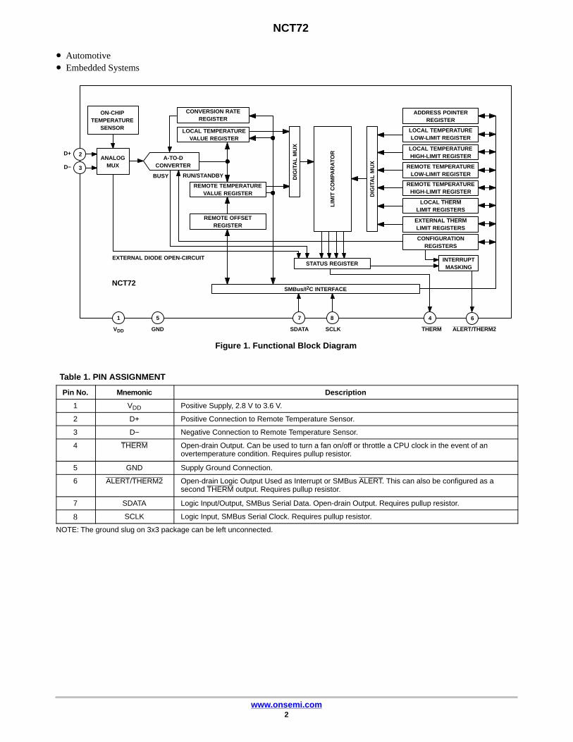
• Automotive• Embedded Systems
Figure 1. Functional Block Diagram
ON-CHIPTEMPERATURE
SENSOR
ANALOGMUX
BUSY
A-TO-DCONVERTER
LOCAL TEMPERATUREVALUE REGISTER
REMOTE OFFSETREGISTER
RUN/STANDBY
EXTERNAL DIODE OPEN-CIRCUITSTATUS REGISTER
SMBus/I2C INTERFACE
LIM
IT C
OM
PAR
AT
OR
DIG
ITA
L M
UX
INTERRUPTMASKING
SDATA SCLK
87
ADDRESS POINTERREGISTER
CONVERSION RATEREGISTER
LOCAL TEMPERATURELOW-LIMIT REGISTER
LOCAL TEMPERATUREHIGH-LIMIT REGISTER
REMOTE TEMPERATURELOW-LIMIT REGISTER
REMOTE TEMPERATUREHIGH-LIMIT REGISTER
LOCAL THERMLIMIT REGISTERS
EXTERNAL THERMLIMIT REGISTERS
CONFIGURATIONREGISTERS
4 6
GND
5
VDD
1
NCT72
D+
ALERT/THERM2THERM
2
D− 3
REMOTE TEMPERATUREVALUE REGISTER D
IGIT
AL
MU
XTable 1. PIN ASSIGNMENT
Pin No. Mnemonic Description
1 VDD Positive Supply, 2.8 V to 3.6 V.
2 D+ Positive Connection to Remote Temperature Sensor.
3 D− Negative Connection to Remote Temperature Sensor.
4 THERM Open-drain Output. Can be used to turn a fan on/off or throttle a CPU clock in the event of anovertemperature condition. Requires pullup resistor.
5 GND Supply Ground Connection.
6 ALERT/THERM2 Open-drain Logic Output Used as Interrupt or SMBus ALERT. This can also be configured as asecond THERM output. Requires pullup resistor.
7 SDATA Logic Input/Output, SMBus Serial Data. Open-drain Output. Requires pullup resistor.
8 SCLK Logic Input, SMBus Serial Clock. Requires pullup resistor.
NOTE: The ground slug on 3x3 package can be left unconnected.

NCT72
www.onsemi.com3
Table 2. ABSOLUTE MAXIMUM RATINGS
Parameter Rating Unit
Positive Supply Voltage (VDD) to GND −0.3, +3.6 V
D+ −0.3 to VDD + 0.3 V
D− to GND −0.3 to +0.6 V
SCLK, SDATA, ALERT, THERM −0.3 to +3.6 V
Input Current, SDATA, THERM −1, +50 mA
Input Current, D− ±1 mA
ESD Rating, All Pins (Human Body Model) 1,500 V
Maximum Junction Temperature (TJ MAX) 150 °C
Storage Temperature Range −65 to +150 °C
Stresses exceeding those listed in the Maximum Ratings table may damage the device. If any of these limits are exceeded, device functionalityshould not be assumed, damage may occur and reliability may be affected.
NOTE: This device is ESD sensitive. Use standard ESD precautions when handling.
Table 3. THERMAL CHARACTERISTICS (Note 1)
Package Type �JA �JC Unit
8-lead DFN 142 43.74 °C/W
1. �JA is specified for the worst-case conditions, that is, a device soldered in a circuit board for surface-mount packages.
Table 4. SMBus/I2C TIMING SPECIFICATIONS (Note 1)
Parameter Limit at TMIN and TMAX Unit Description
fSCLK 400 kHz max −
tLOW 1.3 �s min Clock Low Period, between 10% Points
tHIGH 0.6 �s min Clock High Period, between 90% Points
tR 300 ns max Clock/Data Rise Time
tF 300 ns max Clock/Data Fall Time
tSU; STA 600 ns min Start Condition Setup Time
tHD; STA (Note 2) 600 ns min Start Condition Hold Time
tSU; DAT (Note 3) 100 ns min Data Setup Time
tSU; STO (Note 4) 600 ns min Stop Condition Setup Time
tBUF 1.3 �s min Bus Free Time between Stop and Start Conditions
1. Guaranteed by design, but not production tested.2. Time from 10% of SDATA to 90% of SCLK.3. Time for 10% or 90% of SDATA to 10% of SCLK.4. Time for 90% of SCLK to 10% of SDATA.
Figure 2. Serial Bus Timing
STOPSTART
tSU; DAT
tHIGH
tF
tHD; DAT
tR
tLOW
tSU; STO
STOP START
SCLK
SDATA
tBUF
tHD; STA
tHD; STA
tSU; STA

NCT72
www.onsemi.com4
Table 5. ELECTRICAL CHARACTERISTICS (TA = −40°C to +125°C, VDD = 2.8 V to 3.6 V, unless otherwise noted)
Parameter Conditions Min Typ Max Unit
Power Supply
Supply Voltage, VDD 2.8 3.30 3.6 V
Average Operating Supply Current, IDD 0.0625 Conversions/Sec Rate (Note 1)Standby Mode
−−
2405.0
35030
�A
Undervoltage Lockout Threshold VDD Input, Disables ADC, Rising Edge − 2.55 − V
Power-on Reset Threshold 1.0 − 2.56 V
Temperature-to-digital Converter
Local Sensor Accuracy3.0 V to 3.6 V
0°C ≤ TA ≤ +70°C0°C ≤ TA ≤ +85°C
−−
−−
±1.0±1.5
°C
Local Sensor Accuracy2.8 V to 3.6 V
−20°C ≤ TA ≤ +110°C− − ±2.5
°C
Resolution − 1.0 − °C
Remote Diode Sensor Accuracy3.0 V to 3.6 V
0°C ≤ TA ≤ +70°C, −55°C ≤ TD (Note 2) ≤ +150°C0°C ≤ TA ≤ +85°C, −55°C ≤ TD (Note 2) ≤ +150°C−40°C ≤ TA ≤ +100°C, −55°C ≤ TD (Note 2) ≤ +150°C
−−−
−−−
±1.0±1.5±2.5
°C
Remote Diode Sensor Accuracy3.3 V
−20°C ≤ TA ≤ +70°C, −55°C ≤ TD ≤ +150°C − − ±1.0 °C
Remote Diode Sensor Accuracy2.8 V to 3.6 V
0°C ≤ TA ≤ +70°C, −20°C ≤ TD ≤ +110°C−20°C ≤ TA ≤ +110°C, TD = +40°C
−−
−−
±1.5±2.25
°C
Resolution − 0.25 − °C
Remote Sensor Source Current High Level (Note 3)Middle Level (Note 3)Low Level (Note 3)
−−−
22082
13.5
−−−
�A
Conversion Time From Stop Bit to Conversion Complete, One-shotMode with Averaging Switched On
− 40 52 ms
One-shot Mode with Averaging Off (That Is, Conversion Rate = 16-, 32-, or64-conversions per Second)
− 6.0 8.0 ms
Maximum Series Resistance Cancelled Resistance split evenly on both the D+ and D– inputs − 1.5 − k�
Open-drain Digital Outputs (THERM, ALERT/THERM2)
Output Low Voltage, VOL IOUT = −6.0 mA − − 0.4 V
High Level Output Leakage Current, IOH VOUT = VDD − 0.1 1.0 �A
SMBus/I2C Interface (Note 3 and 4)
Logic Input High Voltage, VIH SCLK, SDATA 1.4 − − V
Logic Input Low Voltage, VIL SCLK, SDATA − − 0.8 V
Hysteresis − 500 − mV
SDA Output Low Voltage, VOL IOUT = −6.0 mA − − 0.4 V
Logic Input Current, IIH, IIL −1.0 − +1.0 �A
SMBus Input Capacitance, SCLK, SDATA − 5.0 − pF
SMBus Clock Frequency − − 400 kHz
SMBus Timeout (Note 5) User Programmable − 25 64 ms
SCLK Falling Edge to SDATA Valid Time Master Clocking in Data − − 1.0 �s
1. See Table 9 for information on other conversion rates.2. Guaranteed by characterization, but not production tested.3. Guaranteed by design, but not production tested.4. See SMBus/I2C Timing Specifications section for more information.5. Disabled by default. Detailed procedures to enable it are in the Serial Bus Interface section of the datasheet.

NCT72
www.onsemi.com5
TYPICAL PERFORMANCE CHARACTERISTICS
Figure 3. Local Temperature Error vs. Temperature Figure 4. Remote Temperature Error vs. ActualTemperature
Figure 5. Temperature Error vs. D+/D− LeakageResistance
Figure 6. Temperature Error vs. D+/D− Capacitance
Figure 7. Operating Supply Current vs.Conversion Rate
Figure 8. Operating Supply Current vs. Voltage
DEV 1DEV 2DEV 3DEV 4DEV 5DEV 6DEV 7
DEV 8DEV 9DEV 10DEV 11DEV 12DEV 13DEV 14
DEV 15DEV 16MEANHIGH 4LOW 4
�
�
DEV 1DEV 2DEV 3DEV 4DEV 5DEV 6DEV 7
DEV 8DEV 9DEV 10DEV 11DEV 12DEV 13DEV 14
DEV 15DEV 16HIGH 4LOW 4
�
�
TEMPERATURE (°C)
−50
TE
MP
ER
AT
UR
E E
RR
OR
(°C
)
−1.00 50 100 150
−0.5
0
0.5
1.0
1.5
2.0
2.5
3.0
3.5
TEMPERATURE (°C)
−50
TE
MP
ER
AT
UR
E E
RR
OR
(°C
)
−1.00 50 100 150
−0.5
0
0.5
1.0
1.5
2.0
2.5
3.0
3.5
LEAKAGE RESISTANCE (M�)
1
TE
MP
ER
AT
UR
E E
RR
OR
(°C
)
−2510 100
−20
−15
−10
−5
0
5
10
D+ To GND
D+ To VDD
CAPACITANCE (nF)
0
TE
MP
ER
AT
UR
E E
RR
OR
(°C
)
−18
DEV 2
5 10 15 20 25
DEV 4
DEV 3
−16
−14
−12
−10
−8
−6
−4
−2
0
CONVERSION RATE (Hz)
0.01
I DD
(�A
)
0
DEV 3BC
0.1 1 10 100
DEV 4BC
DEV 2BC
100
200
300
400
500
600
700
800
900
1000
VDD (V)
3.0
I DD
(�A
)
408
DEV 3BCDEV 4BC
DEV 2BC
3.1 3.2 3.3 3.4 3.5 3.6
410
412
414
416
418
420
422

NCT72
www.onsemi.com6
TYPICAL PERFORMANCE CHARACTERISTICS (Cont’d)
Figure 9. Standby Supply Current vs. Voltage Figure 10. Standby Supply Current vs. ClockFrequency
Figure 11. Temperature Error vs. Common-modeNoise Frequency
Figure 12. Temperature Error vs. Differential-modeNoise Frequency
Figure 13. Temperature Error vs. Series Resistance
VDD (V)
3.0
I DD
(�A
)
3.0
DEV 4
3.1 3.2 3.3 3.4 3.5 3.6
DEV 3
DEV 2
3.2
3.4
3.6
3.8
4.0
4.2
4.4
FSCL (kHz)
1
I ST
BY (�A
)
0
DEV 2BC
10 100 1000
DEV 3BCDEV 4BC
5
10
15
20
25
30
35
NOISE FREQUENCY (MHz)
0
TE
MP
ER
AT
UR
E E
RR
OR
(°C
)
0
100 mV
100 200 300 400 500 600
5
10
15
20
25
20 mV
50 mV
NOISE FREQUENCY (MHz)
0
TE
MP
ER
AT
UR
E E
RR
OR
(°C
)
−10
100 mV
100 200 300 400 500 600
20 mV
50 mV
0
10
20
30
40
50
60
70
80
SERIES RESISTANCE (�)
00
10
20
30
40
50
60
500 1000 1500 2000
TE
MP
ER
AT
UR
E E
RR
OR
(°C
)

NCT72
www.onsemi.com7
Theory of OperationThe NCT72 is a local and remote temperature sensor and
over/under temperature alarm, with the added ability toautomatically cancel the effect of 1.5 k� (typical) ofresistance in series with the temperature monitoring diode.When the NCT72 is operating normally, the on-board ADCoperates in a free running mode. The analog inputmultiplexer alternately selects either the on-chiptemperature sensor to measure its local temperature or theremote temperature sensor. The ADC digitizes these signalsand the results are stored in the local and remote temperaturevalue registers.
The local and remote measurement results are comparedwith the corresponding high, low, and THERM temperaturelimits, stored in eight on-chip registers. Out-of-limitcomparisons generate flags that are stored in the statusregister. A result that exceeds the high temperature limit orthe low temperature limit causes the ALERT output toassert. The ALERT output also asserts if an external diodefault is detected. Exceeding the THERM temperature limitscauses the THERM output to assert low. The ALERT outputcan be reprogrammed as a second THERM output.
The limit registers are programmed and the devicecontrolled and configured via the serial SMBus. Thecontents of any register are also read back via the SMBus.
Control and configuration functions consist of switchingthe device between normal operation and standby mode,selecting the temperature measurement range, masking orenabling the ALERT output, switching Pin 6 betweenALERT and THERM2, and selecting the conversion rate.
Series Resistance CancellationParasitic resistance to the D+ and D− inputs to the NCT72,
seen in series with the remote diode, is caused by a varietyof factors, including PCB track resistance and track length.This series resistance appears as a temperature offset in theremote sensor’s temperature measurement. This errortypically causes a 0.5°C offset per ohm of parasiticresistance in series with the remote diode.
The NCT72 automatically cancels the effect of this seriesresistance on the temperature reading, giving a moreaccurate result, without the need for user characterization ofthis resistance. The NCT72 is designed to automaticallycancel typically up to 1.5 k� of resistance. By using anadvanced temperature measurement method, this process istransparent to the user. This feature permits resistances to beadded to the sensor path to produce a filter, allowing the partto be used in noisy environments. See the section on NoiseFiltering for more details.
Temperature Measurement MethodA simple method of measuring temperature is to exploit
the negative temperature coefficient of a diode, measuringthe base emitter voltage (VBE) of a transistor operated atconstant current. However, this technique requirescalibration to null the effect of the absolute value of VBE,which varies from device to device.
The technique used in the NCT72 measures the change inVBE when the device operates at three different currents.Previous devices used only two operating currents, but it isthe use of a third current that allows automatic cancellationof resistances in series with the external temperature sensor.
Figure 14 shows the input signal conditioning used tomeasure the output of an external temperature sensor. Thisfigure shows the external sensor as a substrate transistor, butit can equally be a discrete transistor. If a discrete transistoris used, the collector is not grounded but is linked to the base.To prevent ground noise interfering with the measurement,the more negative terminal of the sensor is not referenced toground, but is biased above ground by an internal diode atthe D− input. C1 may be added as a noise filter(a recommended maximum value of 1,000 pF). However, abetter option in noisy environments is to add a filter, asdescribed in the Noise Filtering section. See the LayoutConsiderations section for more information on C1.
To measure �VBE, the operating current through thesensor is switched among three related currents. As shownin Figure 14, N1 × I and N2 × I are different multiples of thecurrent, I. The currents through the temperature diode areswitched between I and N1 × I, giving �VBE1; and thenbetween I and N2 × I, giving �VBE2. The temperature isthen calculated using the two �VBE measurements. Thismethod also cancels the effect of any series resistance on thetemperature measurement.
The resulting �VBE waveforms are passed through a65 kHz low-pass filter to remove noise and then to achopper-stabilized amplifier. This amplifies and rectifies thewaveform to produce a dc voltage proportional to �VBE.The ADC digitizes this voltage producing a temperaturemeasurement. To reduce the effects of noise, digital filteringis performed by averaging the results of 16 measurementcycles for low conversion rates. At rates of 16-, 32-, and64-conversions/second, no digital averaging occurs.
Signal conditioning and measurement of the internaltemperature sensor are performed in the same manner.

NCT72
www.onsemi.com8
Figure 14. Input Signal Conditioning
LOW-PASS FILTERfC = 65 kHz
REMOTESENSING
TRANSISTOR
BIASDIODE
D+
D−
VDDIBIASI N1 × I
VOUT+
VOUT−
To ADC
N2 × I
C1*
*CAPACITOR C1 IS OPTIONAL. IT IS ONLY NECESSARY IN NOISY ENVIRONMENTS. C1 = 1,000 pF MAX.
Temperature Measurement ResultsThe results of the local and remote temperature
measurements are stored in the local and remote temperaturevalue registers and compared with limits programmed intothe local and remote high and low limit registers.
The local temperature value is in Register 0x00 and has aresolution of 1°C. The external temperature value is storedin two registers, with the upper byte in Register 0x01 and thelower byte in Register 0x10. Only the two MSBs in theexternal temperature low byte are used giving the externaltemperature measurement a resolution of 0.25°C. Table 6lists the data format for the external temperature low byte.
Table 6. EXTENDED TEMPERATURE RESOLUTION(REMOTE TEMPERATURE LOW BYTE)
Extended ResolutionRemote Temperature
Low Byte
0.00°C 0 000 0000
0.25°C 0 100 0000
0.50°C 1 000 0000
0.75°C 1 100 0000
When reading the full external temperature value, read theLSB first. This causes the MSB to be locked (that is, theADC does not write to it) until it is read. This feature ensuresthat the results read back from the two registers come fromthe same measurement.
Temperature Measurement RangeThe temperature measurement range for both internal and
external measurements is, by default, 0°C to +127°C.However, the NCT72 can be operated using an extendedtemperature range. The extended measurement range is−64°C to +191°C. Therefore, the NCT72 can be used tomeasure the full temperature range of an external diode,from −55°C to +150°C.
The extended temperature range is selected by settingBit 2 of the configuration register to 1. The temperaturerange is 0°C to 127°C when Bit 2 equals 0. A valid result isavailable in the next measurement cycle after changing thetemperature range.
In extended temperature mode, the upper and lowertemperature that can be measured by the NCT72 is limitedby the remote diode selection. The temperature registers canhave values from −64°C to +191°C. However, mosttemperature sensing diodes have a maximum temperaturerange of −55°C to +150°C. Above +150°C, they may losetheir semiconductor characteristics and approximateconductors instead. This results in a diode short. In this case,a read of the temperature result register gives the last goodtemperature measurement. Therefore, the temperaturemeasurement on the external channel may not be accuratefor temperatures that are outside the operating range of theremote sensor.
It should be noted that although both local and remotetemperature measurements can be made while the part is inextended temperature mode, the NCT72 itself should not beexposed to temperatures greater than those specified in theabsolute maximum ratings section. Further, the device isonly guaranteed to operate as specified at ambienttemperatures from −40°C to +120°C.
Temperature Data FormatThe NCT72 has two temperature data formats. When the
temperature measurement range is from 0°C to 127°C(default), the temperature data format for both internal andexternal temperature results is binary. When themeasurement range is in extended mode, an offset binarydata format is used for both internal and external results.Temperature values are offset by 64°C in the offset binarydata format. Examples of temperatures in both data formatsare shown in Table 7.

NCT72
www.onsemi.com9
Table 7. TEMPERATURE DATA FORMAT(TEMPERATURE HIGH BYTE)
Temperature BinaryOffset Binary
(Note 1)
–55°C 0 000 0000(Note 2)
0 000 1001
0°C 0 000 0000 0 100 0000
+1°C 0 000 0001 0 100 0001
+10°C 0 000 1010 0 100 1010
+25°C 0 001 1001 0 101 1001
+50°C 0 011 0010 0 111 0010
+75°C 0 100 1011 1 000 1011
+100°C 0 110 0100 1 010 0100
+125°C 0 111 1101 1 011 1101
+127°C 0 111 1111 1 011 1111
+150°C 0 111 1111(Note 3)
1 101 0110
1. Offset binary scale temperature values are offset by 64°C.2. Binary scale temperature measurement returns 0°C for all
temperatures < 0°C.3. Binary scale temperature measurement returns 127°C for all
temperatures > 127°C.
The user can switch between measurement ranges at anytime. Switching the range likewise switches the data format.The next temperature result following the switching isreported back to the register in the new format. However, thecontents of the limit registers do not change. It is up to theuser to ensure that when the data format changes, the limitregisters are reprogrammed as necessary. More informationon this is found in the Limit Registers section.
NCT72 RegistersThe NCT72 contains 22, 8-bit registers in total. These
registers store the results of remote and local temperaturemeasurements, high and low temperature limits, andconfigure and control the device. See the Address PointerRegister section through the Consecutive ALERT Registersection of this data sheet for more information on the NCT72registers. Additional details are shown in Table 8 throughTable 12. The entire register map is available in Table 13.
Address Pointer RegisterThe address pointer register itself does not have, nor does
it require, an address because the first byte of every writeoperation is automatically written to this register. The datain this first byte always contains the address of anotherregister on the NCT72 that is stored in the address pointerregister. It is to this register address that the second byte ofa write operation is written, or to which a subsequent readoperation is performed.
The power-on default value of the address pointer registeris 0x00. Therefore, if a read operation is performedimmediately after power-on, without first writing to theaddress pointer, the value of the local temperature is returnedbecause its register address is 0x00.
Temperature Value RegistersThe NCT72 has three registers to store the results of local
and remote temperature measurements. These registers canonly be written to by the ADC and can be read by the userover the SMBus/I2C. The local temperature value register isat Address 0x00.
The external temperature value high byte register is atAddress 0x01, with the low byte register at Address 0x10.The power-on default for all three registers is 0x00.
Configuration RegisterThe configuration register is Address 0x03 at read and
Address 0x09 at write. Its power-on default is 0x00. Onlyfour bits of the configuration register are used. Bit 0, Bit 1,Bit 3, and Bit 4 are reserved; the user does not write to them.
Bit 7 of the configuration register masks the ALERToutput. If Bit 7 is 0, the ALERT output is enabled. This is thepower-on default. If Bit 7 is set to 1, the ALERT output isdisabled. This applies only if Pin 6 is configured as ALERT.If Pin 6 is configured as THERM2, then the value of Bit 7has no effect.
If Bit 6 is set to 0, which is power-on default, the deviceis in operating mode with ADC converting. If Bit 6 is set to1, the device is in standby mode and the ADC does notconvert. The SMBus does, however, remain active instandby mode; therefore, values can be read from or writtento the NCT72 via the SMBus. The ALERT and THERMoutputs are also active in standby mode. Changes made tothe registers in standby mode that affect the THERM orALERT outputs cause these signals to be updated.
Bit 5 determines the configuration of Pin 6 on the NCT72.If Bit 5 is 0 (default), then Pin 6 is configured as an ALERToutput. If Bit 5 is 1, then Pin 6 is configured as a THERM2output. Bit 7, the ALERT mask bit, is only active when Pin 6is configured as an ALERT output. If Pin 6 is set up as aTHERM2 output, then Bit 7 has no effect.
Bit 2 sets the temperature measurement range. If Bit 2 is0 (default value), the temperature measurement range is setbetween 0°C to +127°C. Setting Bit 2 to 1 sets themeasurement range to the extended temperature range(−64°C to +191°C).
Table 8. CONFIGURATION REGISTER BITASSIGNMENTS
Bit Name FunctionPower-on
Default
7 MASK1 0 = ALERT Enabled1 = ALERT Masked
0
6 RUN/STOP 0 = Run1 = Standby
0
5 ALERT/THERM2
0 = ALERT1 = THERM2
0
4, 3 Reserved 0
2 TemperatureRange Select
0 = 0°C to 127°C 1 = Extended Range
0
1, 0 Reserved 0

NCT72
www.onsemi.com10
Conversion Rate RegisterThe conversion rate register is Address 0x04 at read and
Address 0x0A at write. The lowest four bits of this registerare used to program the conversion rate by dividing theinternal oscillator clock by 1, 2, 4, 8, 16, 32, 64, 128, 256,512, or 1024 to give conversion times from 15.5 ms(Code 0x0A) to 16 seconds (Code 0x00). For example, aconversion rate of eight conversions per second means thatbeginning at 125 ms intervals, the device performs aconversion on the internal and the external temperaturechannels.
The conversion rate register can be written to and readback over the SMBus/I2C. The higher four bits of thisregister are unused and must be set to 0. The default valueof this register is 0x08, giving a rate of 16 conversions persecond. Use of slower conversion times greatly reduces thedevice power consumption.
Table 9. CONVERSION RATE REGISTER CODES
Code Conversion/Second Time
0x00 0.0625 16 s
0x01 0.125 8 s
0x02 0.25 4 s
0x03 0.5 2 s
0x04 1 1 s
0x05 2 500 ms
0x06 4 250 ms
0x07 8 125 ms
0x08 16 62.5 ms
0x09 32 31.25 ms
0x0A 64 15.5 ms
0x0B to 0xFF Reserved −
Limit RegistersThe NCT72 has eight limit registers: high, low, and
THERM temperature limits for both local and remotetemperature measurements. The remote temperature highand low limits span two registers each, to contain an upperand lower byte for each limit. There is also a THERMhysteresis register. All limit registers can be written to, andread back over, the SMBus. See Table 13 for details of thelimit register addresses and their power-on default values.
When Pin 6 is configured as an ALERT output, the highlimit registers perform a > comparison, while the low limitregisters perform a ≤ comparison. For example, if the highlimit register is programmed with 80°C, then measuring81°C results in an out-of-limit condition, setting a flag in thestatus register. If the low limit register is programmed with0°C, measuring 0°C or lower results in an out-of-limitcondition.
Exceeding either the local or remote THERM limit assertsTHERM low. When Pin 6 is configured as THERM2,exceeding either the local or remote high limit assertsTHERM2 low. A default hysteresis value of 10°C is
provided that applies to both THERM channels. Thishysteresis value can be reprogrammed to any value afterpowerup (Register Address 0x21).
It is important to remember that the temperature limitsdata format is the same as the temperature measurement dataformat. Therefore, if the temperature measurement usesdefault binary, then the temperature limits also use thebinary scale. If the temperature measurement scale isswitched, however, the temperature limits do notautomatically switch. The user must reprogram the limitregisters to the desired value in the correct data format. Forexample, if the remote low limit is set at 10°C with thedefault binary scale, the limit register value is 0000 1010b.If the scale is switched to offset binary, the value in the lowtemperature limit register needs to be reprogrammed to0100 1010b.
Status RegisterThe status register is a read-only register at Address 0x02.
It contains status information for the NCT72.When Bit 7 of the status register is high, it indicates that
the ADC is busy converting. The other bits in this registerflag the out-of-limit temperature measurements (Bit 6 toBit 3, and Bit 1 to Bit 0) and the remote sensor open circuit(Bit 2).
If Pin 6 is configured as an ALERT output, the followingapplies: If the local temperature measurement exceeds itslimits, Bit 6 (high limit) or Bit 5 (low limit) of the statusregister asserts to flag this condition. If the remotetemperature measurement exceeds its limits, then Bit 4(high limit) or Bit 3 (low limit) asserts. Bit 2 asserts to flagan open circuit condition on the remote sensor. These fiveflags are NOR’ed together, so if any of them is high, theALERT interrupt latch is set and the ALERT output goeslow.
Reading the status register clears the five flags, Bit 6 toBit 2, provided the error conditions causing the flags to beset have gone away. A flag bit can be reset only if thecorresponding value register contains an in-limitmeasurement or if the sensor is good.
The ALERT interrupt latch is not reset by reading thestatus register. It resets when the ALERT output has beenserviced by the master reading the device address, providedthe error condition has gone away and the status register flagbits are reset.
When Flag 1 and/or Flag 0 are set, the THERM outputgoes low to indicate that the temperature measurements areoutside the programmed limits. The THERM output doesnot need to be reset, unlike the ALERT output. Once themeasurements are within the limits, the corresponding statusregister bits are automatically reset and the THERM outputgoes high. The user may add hysteresis by programmingRegister 0x21. The THERM output is reset only when thetemperature falls to limit value minus the hysteresis value.
When Pin 6 is configured as THERM2, only the hightemperature limits are relevant. If Flag 6 and/or Flag 4 are

NCT72
www.onsemi.com11
set, the THERM2 output goes low to indicate that thetemperature measurements are outside the programmedlimits. Flag 5 and Flag 3 have no effect on THERM2. Thebehavior of THERM2 is otherwise the same as THERM.
Table 10. STATUS REGISTER BIT ASSIGNMENTS
Bit Name Function
7 BUSY 1 when ADC Is Converting
6 LHIGH(Note 1)
1 when Local High Temperature Limit isTripped
5 LLOW(Note 1)
1 when Local Low Temperature Limit isTripped
4 RHIGH(Note 1)
1 when Remote High Temperature Limitis Tripped
3 RLOW(Note 1)
1 when Remote Low Temperature Limitis Tripped
2 OPEN(Note 1)
1 when Remote Sensor is an OpenCircuit
1 RTHRM 1 when Remote THERM Limit is Tripped
0 LTHRM 1 when Local THERM Limit is Tripped
1. These flags stay high until the status register is read or they arereset by POR unless Pin 6 is configured as THERM2. Then, onlyBit 2 remains high until the status register is read or is reset byPOR.
Offset RegisterOffset errors can be introduced into the remote
temperature measurement by clock noise or when thethermal diode is located away from the hot spot. To achievethe specified accuracy on this channel, these offsets must beremoved.
The offset value is stored as a 10-bit, twos complementvalue in Register 0x11 (high byte) and Register 0x12 (lowbyte, left justified). Only the upper two bits of Register 0x12are used. The MSB of Register 0x11 is the sign bit. Theminimum, programmable offset is −128°C, and themaximum is +127.75°C. The value in the offset register isadded to, or subtracted from, the measured value of theremote temperature.
The offset register powers up with a default value of 0°Cand has no effect unless the user writes a different value toit.
Table 11. SAMPLE OFFSET REGISTER CODES
Offset Value 0x11 0x12
−128°C 1000 0000 00 00 0000
−4°C 1111 1100 00 00 0000
−1°C 1111 1111 00 000000
−0.25°C 1111 1111 10 00 0000
0°C 0000 0000 00 00 0000
+0.25°C 0000 0000 01 00 0000
+1°C 0000 0001 00 00 0000
+4°C 0000 0100 00 00 0000
+127.75°C 0111 1111 11 00 0000
One-shot RegisterThe one-shot register is used to initiate a conversion and
comparison cycle when the NCT72 is in standby mode, afterwhich the device returns to standby. Writing to the one-shotregister address (0x0F) causes the NCT72 to perform aconversion and comparison on both the internal and theexternal temperature channels. This is not a data register assuch, and it is the write operation to Address 0x0F thatcauses the one-shot conversion. The data written to thisaddress is irrelevant and is not stored.
Consecutive ALERT RegisterThe value written to this register determines how many
out-of-limit measurements must occur before an ALERT isgenerated. The default value is that one out-of-limitmeasurement generates an ALERT. The maximum valuethat can be chosen is 4. The purpose of this register is toallow the user to perform some filtering of the output. Thisis particularly useful at the fastest three conversion rates,where no averaging takes place. This register is atAddress 0x22.
Table 12. CONSECUTIVE ALERT REGISTER CODES
Register ValueNumber of Out-of-limit
Measurements Required
yxxx 000x 1
yxxx 001x 2
yxxx 011x 3
yxxx 111x 4
NOTE: x = don’t care bits, and y = SMBus timeout bit.Default = 0. See SMBus section for more information.

NCT72
www.onsemi.com12
Table 13. LIST OF REGISTERS
Read Address (Hex) Write Address (Hex) Name Power-on Default
Not Applicable Not Applicable Address Pointer Undefined
00 Not Applicable Local Temperature Value 0000 0000 (0x00)
01 Not Applicable External Temperature Value High Byte 0000 0000 (0x00)
02 Not Applicable Status Undefined
03 09 Configuration 0000 0000 (0x00)
04 0A Conversion Rate 0000 1000 (0x08)
05 0B Local Temperature High Limit 0101 0101 (0x55) (85°C)
06 0C Local Temperature Low Limit 0000 0000 (0x00) (0°C)
07 0D External Temperature High Limit High Byte 0101 0101 (0x55) (85°C)
08 0E External Temperature Low Limit High Byte 0000 0000 (0x00) (0°C)
Not Applicable 0F (Note 1) One-shot
10 Not Applicable External Temperature Value Low Byte 0000 0000
11 11 External Temperature Offset High Byte 0000 0000
12 12 External Temperature Offset Low Byte 0000 0000
13 13 External Temperature High Limit Low Byte 0000 0000
14 14 External Temperature Low Limit Low Byte 0000 0000
19 19 External THERM Limit 0110 1100 (0x6C) (108°C)
20 20 Local THERM Limit 0101 0101 (0x55) (85°C)
21 21 THERM Hysteresis 0000 1010 (0x0A) (10°C)
22 22 Consecutive ALERT 0000 0001 (0x01)
FE Not Applicable Manufacturer ID 0100 0001 (0x41)
1. Writing to Address 0x0F causes the NCT72 to perform a single measurement. It is not a data register, and it does not matter what data iswritten to it.
Serial Bus InterfaceControl of the NCT72 is carried out via the serial bus. The
NCT72 is connected to this bus as a slave device, under thecontrol of a master device.
The NCT72 has an SMBus/I2C timeout feature. When thisis enabled, the SMBus/I2C times out after typically 25 ms ofno activity. However, this feature is not enabled by default.Bit 7 of the consecutive alert register (Address = 0x22)should be set to enable it.
Addressing the DeviceIn general, every SMBus/I2C device has a 7-bit device
address, except for some devices that have extended 10-bitaddresses. When the master device sends a device addressover the bus, the slave device with that address responds.The NCT72 is available with one device address, 0x4C(1001 100b). An NCT72D is also available.
The NCT72D has an SMBus/I2C address of 0x4D(1001 101b). This is to allow two NCT72 devices on thesame bus, or if the default address conflicts with an existingdevice on the SMBus/I2C. The serial bus protocol operatesas follows:
1. The master initiates a data transfer by establishinga start condition, defined as a high-to-lowtransition on SDATA, the serial data line, whileSCLK, the serial clock line, remains high. Thisindicates that an address/data stream follows. All
slave peripherals connected to the serial busrespond to the start condition and shift in the nexteight bits, consisting of a 7-bit address (MSB first)plus an R/W bit, which determines the direction ofthe data transfer, that is, whether data is written to,or read from, the slave device. The peripheralwhose address corresponds to the transmittedaddress responds by pulling the data line lowduring the low period before the ninth clock pulse,known as the acknowledge bit. All other deviceson the bus remain idle while the selected devicewaits for data to be read from or written to it. If theR/W bit is a 0, the master writes to the slavedevice. If the R/W bit is a 1, the master reads fromthe slave device.
2. Data is sent over the serial bus in a sequence ofnine clock pulses, eight bits of data followed by anacknowledge bit from the slave device. Transitionson the data line must occur during the low periodof the clock signal and remain stable during thehigh period, since a low-to-high transition whenthe clock is high can be interpreted as a stopsignal. The number of data bytes that can betransmitted over the serial bus in a single read orwrite operation is limited only by what the masterand slave devices can handle.

NCT72
www.onsemi.com13
3. When all data bytes have been read or written,stop conditions are established. In write mode, themaster pulls the data line high during the tenthclock pulse to assert a stop condition. In readmode, the master device overrides theacknowledge bit by pulling the data line highduring the low period before the ninth clock pulse.This is known as no acknowledge. The mastertakes the data line low during the low periodbefore the tenth clock pulse, then high during thetenth clock pulse to assert a stop condition. Any number of bytes of data are transferable overthe serial bus in one operation, but it is notpossible to mix read and write in one operationbecause the type of operation is determined at thebeginning and cannot subsequently be changedwithout starting a new operation. For the NCT72,
write operations contain either one or two bytes,while read operations contain one byte.
To write data to one of the device data registers, or to readdata from it, the address pointer register must be set so thatthe correct data register is addressed. The first byte of a writeoperation always contains a valid address that is stored in theaddress pointer register. If data is to be written to the device,the write operation contains a second data byte that is writtento the register selected by the address pointer register.
This procedure is illustrated in Figure 15. The deviceaddress is sent over the bus followed by R/W set to 0. Thisis followed by two data bytes. The first data byte is theaddress of the internal data register to be written to, whichis stored in the address pointer register. The second data byteis the data to be written to the internal data register.
Figure 15. Writing a Register Address to the Address Pointer Register, then Writing Data to the Selected Register
A6
SCLK
SDATA A5 A4 A3 A2 A1 A0 D7 D6 D5 D4 D3 D2 D1 D0
ACK. BYNCT72
START BYMASTER
1 9 1
ACK. BYNCT72
9
D7 D6 D5 D4 D3 D2 D1 D0
ACK. BYNCT72
STOP BYMASTER
1 9
SCLK (CONTINUED)
SDATA (CONTINUED)
FRAME 1SERIAL BUS ADDRESS BYTE
FRAME 2ADDRESS POINTER REGISTER BYTE
FRAME 3DATA BYTE
R/W
Figure 16. Writing to the Address Pointer Register Only
A6
SCLK
SDATA A5 A4 A3 A2 A1 A0 D7 D6 D5 D4 D3 D2 D1 D0
ACK. BYNCT72
STOP BYMASTER
START BYMASTER FRAME 1
SERIAL BUS ADDRESS BYTEFRAME 2
ADDRESS POINTER REGISTER BYTE
1 19
ACK. BYNCT72
9
R/W
Figure 17. Reading Data from a Previously Selected Register
A6
SCLK
SDATA A5 A4 A3 A2 A1 A0 D7 D6 D5 D4 D3 D2 D1 D0
ACK. BYNCT72
STOP BYMASTER
START BYMASTER FRAME 1
SERIAL BUS ADDRESS BYTEFRAME 2
ADDRESS POINTER REGISTER BYTE
1 19
ACK. BYNCT72
9
R/W
NCT72
www.onsemi.com14
When reading data from a register there are twopossibilities.• If the address pointer register value of the NCT72 is
unknown or not the desired value, it is first necessary toset it to the correct value before data can be read fromthe desired data register. This is done by writing to theNCT72 as before, but only the data byte containing theregister read address is sent, because data is not to bewritten to the register see Figure 16.A read operation is then performed consisting of theserial bus address, R/W bit set to 1, followed by thedata byte read from the data register see Figure 17.
• If the address pointer register is known to be at thedesired address, data can be read from the correspondingdata register without first writing to the address pointerregister and the bus transaction shown in Figure 16 canbe omitted.
NOTES:It is possible to read a data byte from a data register withoutfirst writing to the address pointer register. However, if theaddress pointer register is already at the correct value, it isnot possible to write data to a register without writing to theaddress pointer register because the first data byte of a writeis always written to the address pointer register.
Some of the registers have different addresses for read andwrite operations. The write address of a register must bewritten to the address pointer if data is to be written to thatregister, but it may not be possible to read data from thataddress. The read address of a register must be written tothe address pointer before data can be read from thatregister.
ALERT OutputThis is applicable when Pin 6 is configured as an ALERT
output. The ALERT output goes low whenever anout-of-limit measurement is detected, or if the remotetemperature sensor is open circuit. It is an open-drain outputand requires a pullup resistor to VDD. Several ALERT outputscan be wire-OR’ed together, so that the common line goeslow if one or more of the ALERT outputs goes low.
The ALERT output can be used as an interrupt signal to aprocessor, or as an SMBALERT. Slave devices on the SMBuscannot normally signal to the bus master that they want totalk, but the SMBALERT function allows them to do so.
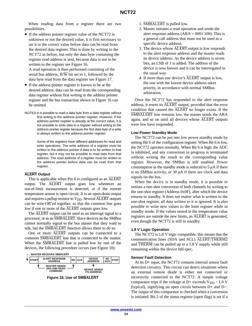
One or more ALERT outputs can be connected to acommon SMBALERT line that is connected to the master.When the SMBALERT line is pulled low by one of thedevices, the following procedure occurs (see Figure 18):
Figure 18. Use of SMBALERT
ALERT RESPONSEADDRESS
MASTER SENDSARA AND READ
COMMAND DEVICE SENDSITS ADDRESS
RDSTART ACK DEVICEADDRESS
NOACK STOP
MASTER RECEIVES SMBALERT
1. SMBALERT is pulled low.2. Master initiates a read operation and sends the
alert response address (ARA = 0001 100). This isa general call address that must not be used as aspecific device address.
3. The device whose ALERT output is low respondsto the alert response address and the master readsits device address. As the device address is sevenbits, an LSB of 1 is added. The address of thedevice is now known and it can be interrogated inthe usual way.
4. If more than one device’s ALERT output is low,the one with the lowest device address takespriority, in accordance with normal SMBusarbitration.
Once the NCT72 has responded to the alert responseaddress, it resets its ALERT output, provided that the errorcondition that caused the ALERT no longer exists. If theSMBALERT line remains low, the master sends the ARAagain, and so on until all devices whose ALERT outputswere low have responded.
Low Power Standby ModeThe NCT72 can be put into low power standby mode by
setting Bit 6 of the configuration register. When Bit 6 is low,the NCT72 operates normally. When Bit 6 is high, the ADCis inhibited, and any conversion in progress is terminatedwithout writing the result to the corresponding valueregister. However, the SMBus is still enabled. Powerconsumption in the standby mode is reduced to 5 �A if thereis no SMBus activity, or 30 �A if there are clock and datasignals on the bus.
When the device is in standby mode, it is possible toinitiate a one-shot conversion of both channels by writing tothe one-shot register (Address 0x0F), after which the devicereturns to standby. It does not matter what is written to theone-shot register, all data written to it is ignored. It is alsopossible to write new values to the limit register while instandby mode. If the values stored in the temperature valueregisters are outside the new limits, an ALERT is generated,even though the NCT72 is still in standby.
1.8 V Logic OperationThe NCT72 is 1.8 V logic compatible; this means that the
communication lines (SDA and SCL) ALERT/THERM2and THERM can be pulled up to a 1.8 V supply while stillremaining within the device Idd spec.
Sensor Fault DetectionAt its D+ input, the NCT72 contains internal sensor fault
detection circuitry. This circuit can detect situations wherean external remote diode is either not connected orincorrectly connected to the NCT72. A simple voltagecomparator trips if the voltage at D+ exceeds VDD − 1.0 V(typical), signifying an open circuit between D+ and D−.The output of this comparator is checked when a conversionis initiated. Bit 2 of the status register (open flag) is set if a

NCT72
www.onsemi.com15
fault is detected. If the ALERT pin is enabled, setting thisflag causes ALERT to assert low.
If the user does not wish to use an external sensor with theNCT72, tie the D+ and D− inputs together to preventcontinuous setting of the open flag.
The NCT72 Interrupt SystemThe NCT72 has two interrupt outputs, ALERT and
THERM. Both have different functions and behavior.ALERT is maskable and responds to violations of softwareprogrammed temperature limits or an open-circuit fault onthe external diode. THERM is intended as a fail-safeinterrupt output that cannot be masked.
If the external or local temperature exceeds theprogrammed high temperature limits, or equals or exceedsthe low temperature limits, the ALERT output is assertedlow. An open-circuit fault on the external diode also causesALERT to assert. ALERT is reset when serviced by a masterreading its device address, provided the error condition hasgone away and the status register has been reset.
The THERM output asserts low if the external or localtemperature exceeds the programmed THERM limits.THERM temperature limits should normally be equal to orgreater than the high temperature limits. THERM is resetautomatically when the temperature falls back within theTHERM limit. A hysteresis value can be programmed; inwhich case, THERM resets when the temperature falls to thelimit value minus the hysteresis value. This applies to bothlocal and remote measurement channels. The power-onhysteresis default value is 10°C, but this can bereprogrammed to any value after powerup.
The hysteresis loop on the THERM outputs is useful whenTHERM is used, for example, as an on/off controller for afan. The user’s system can be set up so that when THERMasserts, a fan is switched on to cool the system. WhenTHERM goes high again, the fan can be switched off.Programming a hysteresis value protects from fan jitter,where the temperature hovers around the THERM limit, andthe fan is constantly switched.
Table 14. THERM HYSTERESIS
THERM Hysteresis Binary Representation
0°C 0 000 0000
1°C 0 000 0001
10°C 0 000 1010
Figure 19 shows how the THERM and ALERT outputsoperate. The ALERT output can be used as a SMBALERTto signal to the host via the SMBus that the temperature has
risen. The user can use the THERM output to turn on a fanto cool the system, if the temperature continues to increase.This method ensures that there is a fail-safe mechanism tocool the system, without the need for host intervention.
Figure 19. Operation of the ALERT and THERMInterrupts
100�C
THERM LIMIT90�C
80�C
70�C
60�C
50�C
40�C
THERM LIMIT − HYSTERESIS
HIGH TEMP LIMIT
RESET BY MASTER
TEMPERATURE
1
2 3
4
ALERT
THERM
• If the measured temperature exceeds the hightemperature limit, the ALERT output asserts low.
• If the temperature continues to increase and exceeds theTHERM limit, the THERM output asserts low. This canbe used to throttle the CPU clock or switch on a fan.
• The THERM output deasserts (goes high) when thetemperature falls to THERM limit minus hysteresis. In ,the default hysteresis value of 10°C is shown.
• The ALERT output deasserts only when thetemperature has fallen below the high temperaturelimit, and the master has read the device address andcleared the status register.
• Pin 6 on the NCT72 can be configured as either anALERT output or as an additional THERM output.
• THERM2 asserts low when the temperature exceeds theprogrammed local and/or remote high temperaturelimits. It is reset in the same manner as THERM and isnot maskable.
• The programmed hysteresis value also applies toTHERM2.
Figure 20 shows how THERM and THERM2 operatetogether to implement two methods of cooling the system.In this example, the THERM2 limits are set lower than theTHERM limits. The THERM2 output is used to turn on afan. If the temperature continues to rise and exceeds theTHERM limits, the THERM output provides additionalcooling by throttling the CPU.

NCT72
www.onsemi.com16
Figure 20. Operation of the THERM and THERM2Interrupts
THERM2 LIMIT
90�C
80�C
70�C
60�C
50�C
40�C
TEMPERATURE
1
2 3
4
THERM
30�C
THERM LIMIT
THERM2
• When the THERM2 limit is exceeded, the THERM2signal asserts low.
• If the temperature continues to increase and exceeds theTHERM limit, the THERM output asserts low.
• The THERM output deasserts (goes high) when thetemperature falls to THERM limit minus hysteresis. InFigure 20, there is no hysteresis value shown.
• As the system cools further, and the temperature fallsbelow the THERM2 limit, the THERM2 signal resets.Again, no hysteresis value is shown for THERM2.
Both the external and internal temperature measurementscause THERM and THERM2 to operate as described.
Application InformationNoise Filtering
For temperature sensors operating in noisy environments,the industry standard practice was to place a capacitor acrossthe D+ and D− pins to help combat the effects of noise.However, large capacitances affect the accuracy of thetemperature measurement, leading to a recommendedmaximum capacitor value of 1,000 pF. Although thiscapacitor reduces the noise, it does not eliminate it, makingit difficult to use the sensor in a very noisy environment.
The NCT72 has a major advantage over other deviceswhen it comes to eliminating the effects of noise on theexternal sensor. The series resistance cancellation featureallows a filter to be constructed between the externaltemperature sensor and the part. The effect of any filterresistance seen in series with the remote sensor isautomatically cancelled from the temperature result.
The construction of a filter allows the NCT72 and theremote temperature sensor to operate in noisy environments.Figure 21 shows a low-pass R-C-R filter, where R = 100��and C = 1 nF. This filtering reduces both common-mode anddifferential noise.
Figure 21. Filter between Remote Sensor and NCT72Factors Affecting Diode Accuracy
100 �
100 �1 nF
D+
D−
REMOTETEMPERATURE
SENSOR
Remote Sensing DiodeThe NCT72 is designed to work with substrate transistors
built into processors or with discrete transistors. Substratetransistors are generally PNP types with the collectorconnected to the substrate. Discrete types are either PNP orNPN transistors connected as diodes (base-shorted tocollector). If an NPN transistor is used, the collector andbase are connected to D+ and the emitter to D−. If a PNPtransistor is used, the collector and base are connected to D−and the emitter to D+.
To reduce the error due to variations in both substrate anddiscrete transistors, consider several factors:• The ideality factor, nF, of the transistor is a measure of
the deviation of the thermal diode from ideal behavior.The NCT72 is trimmed for an nF value of 1.008. Thefollowing equation may be used to calculate the errorintroduced at a temperature, T (°C), when using atransistor whose nF does not equal 1.008. Consult theprocessor data sheet for the nF values.
�T = (nF − 1.008)/1.008 × (273.15 Kelvin + T)
To factor this in, the user writes the �T value to the offsetregister. It is then automatically added to, or subtractedfrom, the temperature measurement.
• Some CPU manufacturers specify the high and lowcurrent levels of the substrate transistors. The highcurrent level of the NCT72, IHIGH, is 220 �A and thelow level current, ILOW, is 13.5 �A. If the NCT72current levels do not match the current levels specifiedby the CPU manufacturer, it may become necessary toremove an offset. The CPU data sheet should advisewhether this offset needs to be removed and how tocalculate it. This offset is programmed to the offsetregister. It is important to note that if more than oneoffset must be considered, the algebraic sum of theseoffsets must be programmed to the offset register.
If a discrete transistor is used with the NCT72, the bestaccuracy is obtained by choosing devices according to thefollowing criteria:• Base-emitter voltage greater than 0.25 V at 6 �A, at the
highest operating temperature• Base-emitter voltage less than 0.95 V at 100 �A, at the
lowest operating temperature

NCT72
www.onsemi.com17
• Base resistance less than 100 �
• Small variation in hFE (50 to 150) that indicates tightcontrol of VBE characteristics
Transistors, such as the 2N3904, 2N3906, or equivalentsin SOT−23 packages are suitable devices to use.
Thermal Inertia and Self-heatingAccuracy depends on the temperature of the remote
sensing diode and/or the internal temperature sensor beingat the same temperature as that being measured. Manyfactors can affect this. Ideally, place the sensor in goodthermal contact with the part of the system being measured.If it is not, the thermal inertia caused by the sensor’s masscauses a lag in the response of the sensor to a temperaturechange. In the case of the remote sensor, this should not bea problem since it is either a substrate transistor in theprocessor or a small package device, such as the SOT−23,placed in close proximity to it.
The on-chip sensor, however, is often remote from theprocessor and only monitors the general ambienttemperature around the package. How accurately thetemperature of the board and/or the forced airflow reflectsthe temperature to be measured dictates the accuracy of themeasurement. Self-heating due to the power dissipated inthe NCT72 or the remote sensor causes the chip temperatureof the device or remote sensor to rise above ambient.However, the current forced through the remote sensor is sosmall that self-heating is negligible. In the case of theNCT72, the worst-case condition occurs when the device isconverting at 64 conversions per second while sinking themaximum current of 1 mA at the ALERT and THERMoutput. In this case, the total power dissipation in the deviceis about 4.5 mW. The thermal resistance, �JA, of the 8-leadDFN is approximately 142°C/W.
Layout ConsiderationsDigital boards can be electrically noisy environments, and
the NCT72 is measuring very small voltages from theremote sensor, so care must be taken to minimize noiseinduced at the sensor inputs. Take the following precautions:• Place the NCT72 as close as possible to the remote
sensing diode. Provided that the worst noise sources,that is, clock generators, data/address buses, and CRTsare avoided, this distance can be 4 inches to 8 inches.
• Route the D+ and D– tracks close together, in parallel,with grounded guard tracks on each side. To minimizeinductance and reduce noise pickup, a 5 mil track widthand spacing is recommended. Provide a ground planeunder the tracks, if possible.
Figure 22. Typical Arrangement of Signal Tracks
5 MIL
5 MIL
5 MIL
5 MIL
5 MIL
5 MIL
5 MIL
GND
D−
D+
GND
• Try to minimize the number of copper/solder joints thatcan cause thermocouple effects. Where copper/solderjoints are used, make sure that they are in both the D+and D− path and at the same temperature.
• Thermocouple effects should not be a major problem as1°C corresponds to about 200 mV, and thermocouplevoltages are about 3 mV/°C of temperature difference.Unless there are two thermocouples with a bigtemperature differential between them, thermocouplevoltages should be much less than 200 mV.
• Place a 0.1 �F bypass capacitor close to the VDD pin. Inextremely noisy environments, place an input filtercapacitor across D+ and D− close to the NCT72. Thiscapacitance can effect the temperature measurement, soensure that any capacitance seen at D+ and D− is, atmaximum, 1,000 pF. This maximum value includes thefilter capacitance, plus any cable or stray capacitancebetween the pins and the sensor diode.
• If the distance to the remote sensor is more than8 inches, the use of twisted pair cable is recommended.A total of 6 feet to 12 feet is needed. For really long distances (up to 100 feet), use a shieldedtwisted pair, such as the Belden No. 8451 microphonecable. Connect the twisted pair to D+ and D− and theshield to GND close to the NCT72. Leave the remoteend of the shield unconnected to avoid ground loops.
Because the measurement technique uses switchedcurrent sources, excessive cable or filter capacitance canaffect the measurement. When using long cables, the filtercapacitance can be reduced or removed.
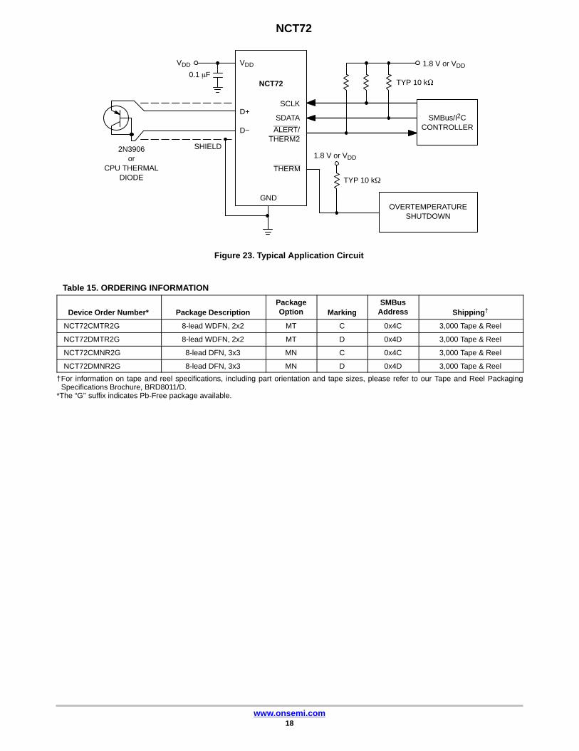
Application CircuitFigure 23 shows a typical application circuit for the
NCT72, using a discrete sensor transistor connected via ashielded, twisted pair cable. The pullups on SCLK, SDATA,and ALERT are required only if they are not providedelsewhere in the system.
NCT72
www.onsemi.com18
Figure 23. Typical Application Circuit
1.8 V or VDD
TYP 10 k�
OVERTEMPERATURESHUTDOWN
SMBus/I2CCONTROLLER
1.8 V or VDD
TYP 10 k�0.1 �F
GND
SHIELD2N3906or
CPU THERMALDIODE
NCT72
SCLK
SDATA
ALERT/THERM2
THERM
VDD
D−
D+
VDD
Table 15. ORDERING INFORMATION
Device Order Number* Package DescriptionPackageOption Marking
SMBusAddress Shipping†
NCT72CMTR2G 8-lead WDFN, 2x2 MT C 0x4C 3,000 Tape & Reel
NCT72DMTR2G 8-lead WDFN, 2x2 MT D 0x4D 3,000 Tape & Reel
NCT72CMNR2G 8-lead DFN, 3x3 MN C 0x4C 3,000 Tape & Reel
NCT72DMNR2G 8-lead DFN, 3x3 MN D 0x4D 3,000 Tape & Reel
†For information on tape and reel specifications, including part orientation and tape sizes, please refer to our Tape and Reel PackagingSpecifications Brochure, BRD8011/D.
*The “G’’ suffix indicates Pb-Free package available.

ÇÇÇÇÇÇÇÇÇÇÇÇ
DFN8 3x3, 0.5PCASE 506BJ−01
ISSUE ODATE 08 NOV 2007SCALE 2:1
GENERICMARKING DIAGRAM*
XXXXX = Specific Device CodeA = Assembly LocationL = Wafer LotY = YearW = Work Week� = Pb−Free Package
*For additional information on our Pb−Free strategy and solderingdetails, please download the ON Semiconductor Soldering andMounting Techniques Reference Manual, SOLDERRM/D.
SOLDERMASK DEFINED*This information is generic. Please refer
to device data sheet for actual partmarking.Pb−Free indicator, “G” or microdot “ �”,may or may not be present.
PIN 1REFERENCE
AB
C0.10
2X
2X
TOP VIEW
D
E
C0.10
NOTES:1. DIMENSIONS AND TOLERANCING PER ASME
Y14.5M, 1994.2. CONTROLLING DIMENSION: MILLIMETERS.3. DIMENSION b APPLIES TO PLATED TERMINAL
AND IS MEASURED BETWEEN 0.15 AND 0.30MM FROM TERMINAL.
4. COPLANARITY APPLIES TO THE EXPOSEDPAD AS WELL AS THE TERMINALS.
1
XXXXXXXXXXALYW�
�
1
E2
BOTTOM VIEW
b0.10
8X
L1 4
0.05
C A B
C
D2
e
K
8 5
8X
8X
(A3)C
C0.058X
C0.05
SIDE VIEW A1
A
SEATINGPLANE
DIM MIN MAXMILLIMETERS
A 0.80 1.00A1 0.00 0.05A3 0.20 REFb 0.18 0.30D 3.00 BSCD2 1.64 1.84E 3.00 BSC
E2 1.35 1.55e 0.50 BSCK 0.20 −−−L 0.30 0.50
NOTE 3
L
DETAIL AOPTIONAL
CONSTRUCTION
L1
DETAIL A
ÉÉÉÉÉÉDETAIL B
EDGE OF PACKAGE
MOLD CMPDEXPOSED Cu
L
OPTIONALCONSTRUCTION
OPTIONALCONSTRUCTION
L1 0.00 0.03
NOTE 4
DETAIL B
3.30
8X
DIMENSION: MILLIMETERS
0.63
1.55
1.85
0.50PITCH
8X0.35
MOUNTING FOOTPRINT
(Note: Microdot may be in either location)
DETAIL A
8
MECHANICAL CASE OUTLINE
PACKAGE DIMENSIONS
ON Semiconductor and are trademarks of Semiconductor Components Industries, LLC dba ON Semiconductor or its subsidiaries in the United States and/or other countries.ON Semiconductor reserves the right to make changes without further notice to any products herein. ON Semiconductor makes no warranty, representation or guarantee regardingthe suitability of its products for any particular purpose, nor does ON Semiconductor assume any liability arising out of the application or use of any product or circuit, and specificallydisclaims any and all liability, including without limitation special, consequential or incidental damages. ON Semiconductor does not convey any license under its patent rights nor therights of others.
98AON25786DDOCUMENT NUMBER:
DESCRIPTION:
Electronic versions are uncontrolled except when accessed directly from the Document Repository.Printed versions are uncontrolled except when stamped “CONTROLLED COPY” in red.
PAGE 1 OF 1DFN8 3X3, 0.5P
© Semiconductor Components Industries, LLC, 2019 www.onsemi.com

ÍÍÍÍÍÍ
C
A
SEATINGPLANE
D
E
0.10 C
A3
A
A1
0.10 C
WDFN8 2x2, 0.5PCASE 511AT−01
ISSUE ODATE 26 FEB 2010
SCALE 4:1
DIMA
MIN MAXMILLIMETERS
0.70 0.80A1 0.00 0.05A3 0.20 REFb 0.20 0.30DEeL
PIN ONEREFERENCE
0.05 C
0.05 C
A0.10 C
NOTE 3
L2
e
bB
4
88X
1
5
0.05 C
L1
2.00 BSC2.00 BSC0.50 BSC
0.40 0.60--- 0.15
BOTTOM VIEW
L7X
L1
DETAIL A
L
ALTERNATE TERMINALCONSTRUCTIONS
L
ÉÉÉÉÉÉÉÉÉ
DETAIL B
MOLD CMPDEXPOSED Cu
ALTERNATECONSTRUCTIONS
DETAIL B
DETAIL A
L2 0.50 0.70
B
TOP VIEW
SIDE VIEW
NOTES:1. DIMENSIONING AND TOLERANCING PER
ASME Y14.5M, 1994.2. CONTROLLING DIMENSION: MILLIMETERS.3. DIMENSION b APPLIES TO PLATED
TERMINAL AND IS MEASURED BETWEEN0.15 AND 0.30 MM FROM TERMINAL TIP.
*For additional information on our Pb−Free strategy and solderingdetails, please download the ON Semiconductor Soldering andMounting Techniques Reference Manual, SOLDERRM/D.
SOLDERING FOOTPRINT*
2.30
0.50
0.787X
DIMENSIONS: MILLIMETERS0.30 PITCH
*This information is generic. Please refer todevice data sheet for actual part marking.Pb−Free indicator, “G” or microdot “ �”,may or may not be present.
GENERICMARKING DIAGRAM*
8X
1
PACKAGEOUTLINE
RECOMMENDED
XX = Specific Device CodeM = Date Code� = Pb−Free Device
XXM�
�
1
0.88
(Note: Microdot may be in either location)
2X
2X
8X
e/2
MECHANICAL CASE OUTLINE
PACKAGE DIMENSIONS
ON Semiconductor and are trademarks of Semiconductor Components Industries, LLC dba ON Semiconductor or its subsidiaries in the United States and/or other countries.ON Semiconductor reserves the right to make changes without further notice to any products herein. ON Semiconductor makes no warranty, representation or guarantee regardingthe suitability of its products for any particular purpose, nor does ON Semiconductor assume any liability arising out of the application or use of any product or circuit, and specificallydisclaims any and all liability, including without limitation special, consequential or incidental damages. ON Semiconductor does not convey any license under its patent rights nor therights of others.
98AON48654EDOCUMENT NUMBER:
DESCRIPTION:
Electronic versions are uncontrolled except when accessed directly from the Document Repository.Printed versions are uncontrolled except when stamped “CONTROLLED COPY” in red.
PAGE 1 OF 1WDFN8, 2X2, 0.5 P
© Semiconductor Components Industries, LLC, 2019 www.onsemi.com

onsemi, , and other names, marks, and brands are registered and/or common law trademarks of Semiconductor Components Industries, LLC dba “onsemi” or its affiliatesand/or subsidiaries in the United States and/or other countries. onsemi owns the rights to a number of patents, trademarks, copyrights, trade secrets, and other intellectual property.A listing of onsemi’s product/patent coverage may be accessed at www.onsemi.com/site/pdf/Patent−Marking.pdf. onsemi reserves the right to make changes at any time to anyproducts or information herein, without notice. The information herein is provided “as−is” and onsemi makes no warranty, representation or guarantee regarding the accuracy of theinformation, product features, availability, functionality, or suitability of its products for any particular purpose, nor does onsemi assume any liability arising out of the application or useof any product or circuit, and specifically disclaims any and all liability, including without limitation special, consequential or incidental damages. Buyer is responsible for its productsand applications using onsemi products, including compliance with all laws, regulations and safety requirements or standards, regardless of any support or applications informationprovided by onsemi. “Typical” parameters which may be provided in onsemi data sheets and/or specifications can and do vary in different applications and actual performance mayvary over time. All operating parameters, including “Typicals” must be validated for each customer application by customer’s technical experts. onsemi does not convey any licenseunder any of its intellectual property rights nor the rights of others. onsemi products are not designed, intended, or authorized for use as a critical component in life support systemsor any FDA Class 3 medical devices or medical devices with a same or similar classification in a foreign jurisdiction or any devices intended for implantation in the human body. ShouldBuyer purchase or use onsemi products for any such unintended or unauthorized application, Buyer shall indemnify and hold onsemi and its officers, employees, subsidiaries, affiliates,and distributors harmless against all claims, costs, damages, and expenses, and reasonable attorney fees arising out of, directly or indirectly, any claim of personal injury or deathassociated with such unintended or unauthorized use, even if such claim alleges that onsemi was negligent regarding the design or manufacture of the part. onsemi is an EqualOpportunity/Affirmative Action Employer. This literature is subject to all applicable copyright laws and is not for resale in any manner.
PUBLICATION ORDERING INFORMATIONTECHNICAL SUPPORTNorth American Technical Support:Voice Mail: 1 800−282−9855 Toll Free USA/CanadaPhone: 011 421 33 790 2910
LITERATURE FULFILLMENT:Email Requests to: [email protected]
onsemi Website: www.onsemi.com
Europe, Middle East and Africa Technical Support:Phone: 00421 33 790 2910For additional information, please contact your local Sales Representative
◊