Embed Size (px)
Citation preview

© Semiconductor Components Industries, LLC, 2015
December, 2020 − Rev. 61 Publication Order Number:
NCP1256/D
Low Power Offline PWM
Current Mode Controller
with Brown-Out Protection
NCP1256
The NCP1256 includes everything to build cost−effective switchmode power supplies ranging from a few watts up to several tens ofwatts. Housed in a tiny TSOP−6 package, the part can be supplied upto 30 V. It hosts a jittered 65 or 100−kHz switching circuitry operatedin peak current mode control. When the power in the secondary sidestarts decreasing, the controller automatically folds back its switchingfrequency down to a minimum level of 26 kHz. As the power furthergoes down, the part enters skip cycle while freezing the peak current.
NCP1256 comes with several protection features such as atimer−based auto−recovery short circuit protection, lossless OPP, andan easily adjustable Brown Out (BO) pin. Two inputs are provided tolatch off the part in a practical way, for instance with OVP and OTPevents. Several options exists to chose latch or auto−recovery for theseevents.
Features• Fixed−frequency 65−kHz or 100−kHz Current−mode Control
Operation• Adjustable Over Power Protection (OPP) Circuit, Disabled at Low
Line• Adjustable Brown Out Level
• Frequency Foldback down to 26 kHz and Skip−cycle in Light LoadConditions
• Internally−fixed Slope Compensation Ramp
• Internally−fixed 4−ms Soft−start
• 70−ms Timer−based Auto−recovery Short−circuit Protection
• Frequency Jittering in Normal and Frequency Foldback Modes
• Double Hiccup Auto−recovery Short−circuit Protection
• Pre−short Ready for Latched OCP Option
• Latched/Auto−Recovery OVP Protection on Vcc
• Latched Inputs for Improved Robustness (OVP and OTPimplementations)
• Auto−Recovery ac Line OVP Protection (E Version)
• +500 mA/ −500 mA Source/Sink Drive Capability
• EPS 2.0 Compliant
• These are Pb−Free Devices
Typical Applications• Ac−dc Adapters for Portable Devices, Computers, Tablets etc.
• Auxiliary Power Supplies
PIN CONNECTIONS
1
3 CS
GND
2
BO 4
DRV6
(Top View)
5 VCC
TSOP−6CASE 318GSTYLE 13
MARKING DIAGRAM
FB
www.onsemi.com
(Note: Microdot may be in either location)
1
6xxAYW�
�
1
6xx = Specific Device Codex = A, E or 2A = Assembly LocationY = YearW = Work Week� = Pb−Free Package
See detailed ordering and shipping information in the packagedimensions section on page 23 of this data sheet.
ORDERING INFORMATION

NCP1256
www.onsemi.com2
1
2
3
6
4
5
NCP1256
Vbulk
..
OPPadjust
Vout
.
Figure 1. Typical Application Example – Latched OVP on Vcc
1
2
3
6
4
5
Vbulk
..
OPPadjust
Vout
.
NCP1256
Figure 2. Typical Application Example – OVP is Latched on BO

NCP1256
www.onsemi.com3
1
2
3
6
4
5
NCP1256
Vbulk
..
OPPadjust
Vout
.
Figure 3. Typical Application Example – OVP is Latched on Vcc, OTP Latched on CS
Table 1. PIN DESCRIPTIONS
Pin No Pin Name Function Pin Description
1 GND − The controller ground.
2 FB Feedback pin Hooking an optocoupler collector to this pin will allow regulation.
3 BO/OVP Adjust the BO levelLatch input
A voltage below the programmed level stops the controller. Whenabove, the controller can start. When the pin is brought above4.5 V for four consecutive clock cycles, the part latches off. Withthe E version, an auto−recovery ac line OVP is available throughthis pin.
4 CS Current sense + OPP adjustmentLatch input
This pin monitors the primary peak current but also offers ameans to introduce over power compensation. When the pin isbrought above 1.5 V during the off time, the part permanentlylatches off.
5 Vcc Supplies the controller – protects the IC
This pin is connected to an external auxiliary voltage. An OVPcomparator monitors this pin and offers a means to latch the con-verter in fault conditions.
6 DRV Driver output The driver’s output to an external MOSFET gate.
Table 2. OPTIONS
Controller Frequency OCP OVP on BOOVP/OTP
CSOVPVcc
NCP1256ASN65T1G 65 kHz Latched Latched Latched Latched
NCP1256BSN65T1G 65 kHz Auto−recovery Latched Latched Latched
NCP1256ASN100T1G 100 kHz Latched Latched Latched Latched
NCP1256BSN100T1G 100 kHz Auto−recovery Latched Latched Latched
NCP1256ESN65T1G 65 kHz Auto−recovery Auto−recovery Auto−recovery Auto−recovery
NCP1256
www.onsemi.com4
S
R
Q
Q
65/100kHz clock
Jittermod.
Vcc
Drv
Vcc and logicmanagement
Vdd
poweron reset
LEB1
vdd
/ 3
4 msSS
Power onreset
GNDCS
FB
1−us timeconstant
Frequencyfoldback
Vsk
ip
Vlatch1
Vfold
S
R
Q
Q
Clamp
Up counter
4
doublehiccup
RST
Eventgone?
peak currentfreeze
VFB < 0.75 V ? setpoint = 250 mV
UVLO
BO
VBO1VBO2
BO
VOVP
20 us
Ipflag = 1 if over current−−> start timer −−> auto rec.+
invert
slope compensation
vdd
OPPGM
IOPPLLVlatch2
RFB
Validatedduring off time (option)
ICSO
Pre−shortLatched OCP(option)
UVLO?checked atPON only
latched OCP opt.
Iopp3
VFB < VfoldF Iopp3 = 0VFB > VoppF Iopp3 = I1
I2=0I1=I2
VFB
RdBO
DZBO
I1 I2
BOreset
= 1 if timercompleted
OCP timer completedAuto−recovery dble hiccup
OVP on BO OVP on CSLogicmngt
1−us timeconstant
Figure 4. Internal Block Diagram
Auto−recoveryfor E version
no clampfor E version
Table 3. MAXIMUM RATINGS TABLE
Symbol Rating Value Unit
Vcc Power Supply voltage, Vcc pin, continuous voltage −0.3 to 28 V
Maximum voltage on low power pins CS, FB and BO −0.3 to 10 V
VDRV Maximum voltage on DRV pin −0.3 to Vcc+0.3 V
RθJ−A Thermal Resistance Junction−to−Air 360 °C/W
TJ,max Maximum Junction Temperature 150 °C
Storage Temperature Range −60 to +150 °C
HBM Human Body Model ESD Capability per JEDEC JESD22−A114F 4 kV
MM Machine Model ESD Capability per JEDEC JESD22−A115C 200 V
CDM Charged−Device Model ESD Capability per JEDEC JESD22−C101E 750 V
Stresses exceeding those listed in the Maximum Ratings table may damage the device. If any of these limits are exceeded, device functionalityshould not be assumed, damage may occur and reliability may be affected.

NCP1256
www.onsemi.com5
Table 4. ELECTRICAL CHARACTERISTICS (For typical values TJ = 25°C, for min/max values TJ = −40°C to +125°C, Max TJ = 150°C, Vcc = 12 V unless otherwise noted)
Symbol Rating Pin Min Typ Max Unit
SUPPLY SECTION
VCCON VCC increasing level at which driving pulses are authorized 5 16 18 20 V
VCC(min) VCC decreasing level at which driving pulses are stopped 5 8.3 8.9 9.5 V
VCCHYST Hysteresis VccON−Vcc(min) 5 8.4 − 9.25 V
VCCreset Latched state reset voltage 5 8.1 VCC(min)−250 mV
8.8 V
ICC1 Start−up current 5 5 7.5 �A
ICC2 Internal IC consumption with VFB = 3.2 V and CL = 0FSW = 65 kHzFSW = 100 kHz
5−−
1.301.35
−−
mA
ICC3 Internal IC consumption with VFB = 3.2 V and CL = 1 nFFSW = 65 kHzFSW = 100 kHz
5−−
1.82.5
−−
mA
Idis Natural part consumption in hiccup mode – non switching 5 − 350 − �A
ICCstby Static consumption between two skip cycles 5 − 420 − �A
ICCnoload Internal IC consumption while in skip mode (Vcc = 14 V, driving a typi-cal 7−A/600−V MOSFET, includes opto current) (Note 1)
5 − 440 − �A
DRIVE SECTION
Tr Output voltage rise−time @ CL = 1 nF, 10−90% of output signal 6 − 40 − ns
Tf Output voltage fall−time @ CL = 1 nF, 10−90% of output signal 6 − 30 − ns
ROH Source resistance 6 − 13 − �
ROL Sink resistance 6 − 6 − �
Isource Peak source current, VGS = 0 V (Note 2) 6 − 500 − mA
Isink Peak sink current, VGS = 12 V (Note 2) 6 − 500 − mA
VDRVlow DRV pin level at VCC close to VCC(min) with a 33−k� resistor to GND 6 8 − − V
VDRVhigh DRV pin level at VCC= VOVP−0.2 V – DRV unloaded 6 10 12 14 V
CURRENT COMPARATOR
VLimit Maximum internal current setpoint – no OPP 4 0.744 0.8 0.856 V
VfoldI Default internal voltage set point for frequency foldback trip point ≈ 63%of Vlimit
4 − 500 − mV
VfreezeI Internal peak current setpoint freeze (≈31% of Vlimit) 4 − 250 − mV
TDEL Propagation delay from current detection to gate off−state 4 − 40 60 ns
TLEB1 Leading Edge Blanking Duration – first OCP path 4 − 300 − ns
TSS Internal soft−start duration activated upon startup, auto−recovery − − 4 − ms
ICSO Internal pull−up source for pin opening safety test 4 − 1 − �A
IOPP1 Voltage on VFB < VfoldF, percentage of applied OPP current 4 − 0 − %
IOPP2 Voltage on VFB > VfoldF + 0.7 V, percentage of applied OPP current 4 − 100 − %
IOPP3 Voltage on pin 3 = 2.65 V (265 V rms in) AND VFB > VfoldF 4 170 185 210 �A
IOPP3clp Voltage on pin 3 > 2.65 V – clamped OPP current 4 − 185 − �A
IOPPLL OPP current delivered from CS pin for Vpin3 = VBOon 4 − − 6 �A
OPPgm Internal OTA for OPP current generation from BO−40°C to +125°C+25°C to +125°C
4101103
115115
125125
�S

NCP1256
www.onsemi.com6
Table 4. ELECTRICAL CHARACTERISTICS (continued)(For typical values TJ = 25°C, for min/max values TJ = −40°C to +125°C, Max TJ = 150°C, Vcc = 12 V unless otherwise noted)
Symbol UnitMaxTypMinPinRating
INTERNAL OSCILLATOR
fOSC,nom Oscillation Frequency65 kHz version100 kHz version
−6193
65100
70107
kHz
Dmax Maximum duty ratio − 77 80 83 %
fjitter Frequency jittering in percentage of fOSC − − ±5 − %
fswing Swing frequency over the whole frequency range − − 240 − Hz
FEEDBACK SECTION
Rup Internal pull−up resistor 2 − 30 − k�
Req Equivalent ac resistance from FB to gnd 2 19 23 26 k�
Iratio Pin 2 to current setpoint division ratio − − 3 −
VfreezeF Feedback voltage below which the peak current is frozen 2 − 0.75 − V
FREQUENCY FOLDBACK
VfoldF Frequency foldback level on the feedback pin – ≈63% of maximumpeak current
− − 1.5 − V
Ftrans Minimum operating frequency − 22 26 30 kHz
Vfold,end End of frequency foldback feedback level, Fsw = Ftrans − 1.2 − V
Vskip Skip−cycle level voltage on the feedback pin − − 0.6 − V
Skiphysteresis
Hysteresis on the skip comparator (Note 3) − − 45 − mV
INTERNAL SLOPE COMPENSATION
S65 Compensation ramp slope, Fsw = 65 kHz − − 30 − mV/�s
S100 Compensation ramp slope, Fsw = 100 kHz − − 50 − mV/�s
PROTECTIONS
Vlatch1 Latching level input, brown−out input 3 4.3 4.5 4.7 V
Vlatch2 Latching level, current sense input, off time only 4 1.45 1.5 1.55 V
Tlatch−count Number of clock cycles before latch confirmation from pin 3&4 − − 4 −
Tlatch−del OVP detection time constant − 1 − �s
Timer Internal auto−recovery fault timer duration − 50 70 90 ms
VOVP Latched over voltage protection on the Vcc rail 6 25.3 26 26.8 V
TOVP−del Delay before OVP confirmation on Vcc 6 − 25 − �s
IBO Brown−Out input bias current, VBO < DZBO 3 − 0.02 − �A
VBOon Turn−on voltage 3 0.76 0.8 0.87 V
VBOoff Turn−off voltage 3 0.66 0.7 0.74 V
TBO De−bouncing filter on BO comparator 3 − 50 − �s
RdBO Dynamic Zener diode resistance (all versions except E) 3 − 1 − k�
DZBO Active Zener diode clamping BO signal (all versions except E) 3 3.1 3.3 3.5 V
DZBO Active Zener diode clamping BO signal (all versions except E) 3 3.1 3.3 3.5 V
Product parametric performance is indicated in the Electrical Characteristics for the listed test conditions, unless otherwise noted. Productperformance may not be indicated by the Electrical Characteristics if operated under different conditions.1. For information only, collected on a typical 45−W adapter.2. Guaranteed by design3. Not tested in production.

NCP1256
www.onsemi.com7
TYPICAL CHARACTERISTICS
Figure 5. VCC(on) vs. Junction Temperature Figure 6. VCC(off) vs. Junction Temperature
JUNCTION TEMPERATURE (°C) JUNCTION TEMPERATURE (°C)
1501007550250−25−5016.0
16.5
17.0
17.5
18.0
19.0
19.5
20.0
1501007550250−25−508.3
8.5
8.7
8.9
9.1
9.3
9.5
Figure 7. ICC1 vs. Junction Temperature Figure 8. ICC3 vs. Junction Temperature
JUNCTION TEMPERATURE (°C) JUNCTION TEMPERATURE (°C)
1501007550250−25−502
3
4
5
7
8
9
10
1501007550250−25−501.51.6
1.8
1.9
2.0
2.2
2.4
2.5
Figure 9. ICC3 vs. Junction Temperature Figure 10. ICCstby vs. Junction Temperature
JUNCTION TEMPERATURE (°C) JUNCTION TEMPERATURE (°C)
1251007550250−25−502.02.1
2.3
2.4
2.5
2.7
2.9
3.0
1501007550250−25−50300320
360
380
420
440
480
500
VC
C(o
n) (
V)
VC
C(o
ff) (
V)
ICC
1 (�
A)
ICC
3 (6
5 kH
z) (
mA
)
ICC
3 (1
00 k
Hz)
(m
A)
ICC
stby
(�A
)
125
125
150
125
125
125
18.5
6
1.7
2.1
2.3
2.2
2.6
2.8
340
400
460

NCP1256
www.onsemi.com8
TYPICAL CHARACTERISTICS
Figure 11. VLimit vs. Junction Temperature Figure 12. Vfoldl vs. Junction Temperature
JUNCTION TEMPERATURE (°C) JUNCTION TEMPERATURE (°C)
1501007550250−25−500.744
0.764
0.784
0.804
0.824
0.844
1501007550250−25−500.45
0.47
0.49
0.51
0.53
0.55
Figure 13. VFreezel vs. Junction Temperature Figure 14. TDEL vs. Junction Temperature
JUNCTION TEMPERATURE (°C) JUNCTION TEMPERATURE (°C)
1501007550250−25−500.20
0.22
0.24
0.26
0.28
0.30
1501007550250−25−505
15
25
35
45
55
Figure 15. TLEB1 vs. Junction Temperature Figure 16. IOPP3 vs. Junction Temperature
JUNCTION TEMPERATURE (°C) JUNCTION TEMPERATURE (°C)
1251007550250−25−50200220
260
280
300
340
380
400
1501007550250−25−50170
175
180
185
190
200
205
210
VLi
mit
(V)
Vfo
ldl (
V)
VF
reez
el (
V)
TD
EL
(ns)
TLE
B1
(ns)
IOP
P3
(�A
)
125
125
150
125
125
125
240
320
360
195

NCP1256
www.onsemi.com9
TYPICAL CHARACTERISTICS
Figure 17. fOSC(nom) vs. JunctionTemperature
Figure 18. fOSC(nom) vs. JunctionTemperature
JUNCTION TEMPERATURE (°C) JUNCTION TEMPERATURE (°C)
1501007550250−25−5061
62
63
65
66
67
69
70
1501007550250−25−5093
95
97
99
101
103
105
107
Figure 19. Dmax vs. Junction Temperature Figure 20. Req vs. Junction Temperature
JUNCTION TEMPERATURE (°C) JUNCTION TEMPERATURE (°C)
1501007550250−25−5077
78
79
80
81
82
83
1501007550250−25−5019
20
21
22
23
24
25
26
Figure 21. VfreezeF vs. Junction Temperature Figure 22. VfoldF vs. Junction Temperature
JUNCTION TEMPERATURE (°C) JUNCTION TEMPERATURE (°C)
1251007550250−25−500.650.67
0.69
0.71
0.77
0.79
0.81
0.85
1501007550250−25−501.30
1.35
1.40
1.45
1.55
1.60
1.65
1.70
fOS
C(n
om)
65 k
Hz
(kH
z)
fOS
C(n
om)
100
kHz
(kH
z)
Dm
ax (
%)
Req
(k�
)
Vfr
ezze
F (
V)
Vfo
ldF
(V
)
125
125
150
125
125
125
64
68
0.73
0.75
0.83
1.50
NCP1256
www.onsemi.com10
TYPICAL CHARACTERISTICS
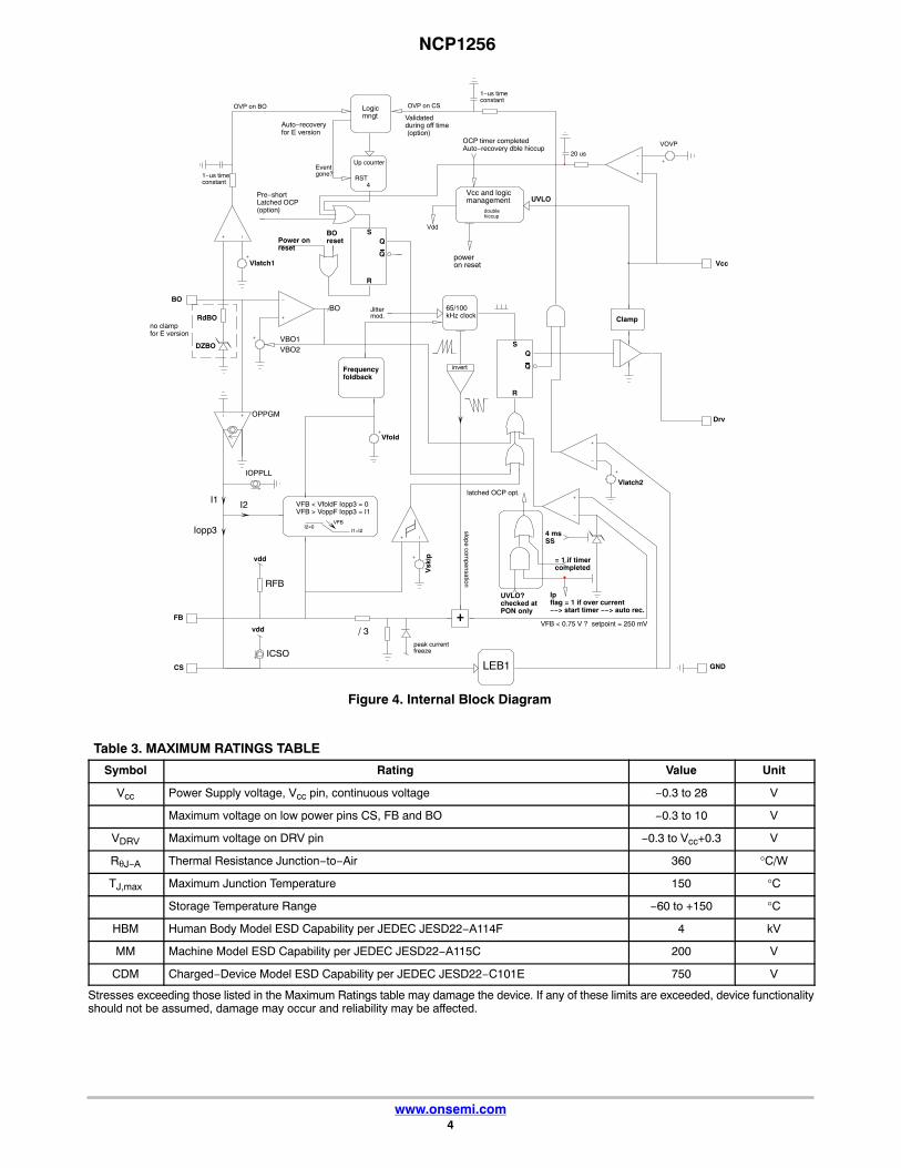
Figure 23. Vfold,end vs. Junction Temperature Figure 24. Ftrans vs. Junction Temperature
JUNCTION TEMPERATURE (°C) JUNCTION TEMPERATURE (°C)
1501007550250−25−501.00
1.05
1.10
1.20
1.25
1.30
1.35
1.40
1501007550250−25−5022
23
24
25
27
28
29
30
Figure 25. Vskip vs. Junction Temperature Figure 26. Vlatch1 vs. Junction Temperature
JUNCTION TEMPERATURE (°C) JUNCTION TEMPERATURE (°C)
1501007550250−25−50550560
580
590
600
620
640
650
1501007550250−25−504.30
4.35
4.40
4.45
4.50
4.60
4.65
4.70
Figure 27. Vlatch2 vs. Junction Temperature Figure 28. Timer vs. Junction Temperature
JUNCTION TEMPERATURE (°C) JUNCTION TEMPERATURE (°C)
1251007550250−25−501.45
1.47
1.49
1.51
1.53
1.55
1501007550250−25−5050
55
60
65
70
80
85
90
Vfo
ld,e
nd (
V)
Ftr
ans
(kH
z)
Vsk
ip (
mV
)
Vla
tch1
(V
)
Vla
tch2
(V
)
Tim
er (
ms)
125
125
150
125
125
125
1.15
26
570
610
630
4.55
75

NCP1256
www.onsemi.com11
TYPICAL CHARACTERISTICS
Figure 29. VOVP vs. Junction Temperature Figure 30. VBOon vs. Junction Temperature
JUNCTION TEMPERATURE (°C) JUNCTION TEMPERATURE (°C)
1501007550250−25−5025.3
25.5
25.7
25.9
26.1
26.3
26.5
26.7
1501007550250−25−500.76
0.77
0.78
0.79
0.81
0.82
0.83
0.84
Figure 31. VCCreset vs. Junction Temperature Figure 32. RdBO vs. Junction Temperature
JUNCTION TEMPERATURE (°C) JUNCTION TEMPERATURE (°C)
1501007550250−25−508.08.1
8.3
8.4
8.6
8.7
8.9
9.0
1501007550250−25−500.50.6
0.8
0.9
1.0
1.2
1.3
1.5
Figure 33. DZBO vs. Junction Temperature
JUNCTION TEMPERATURE (°C)
1251007550250−25−503.10
3.15
3.20
3.30
3.35
3.40
3.45
3.50
VO
VP
(V
)
VB
Oon
(V
)
VC
Cre
set (
V)
RdB
O (
k�)
DZ
BO
(V
)
125
125
150
125
125
0.80
8.2
8.5
8.8
0.7
1.1
1.4
3.25
NCP1256
www.onsemi.com12
APPLICATION INFORMATION
NCP1256 implements a standard current modearchitecture where the switch−off event is dictated by thepeak current setpoint. This component represents the idealcandidate where low part−count and cost effectiveness arekey design parameters, particularly in low−cost ac−dcadapters, open−frame power supplies etc. NCP1256 bringsall the necessary components normally needed in todaymodern power supply designs, bringing severalenhancements such as a non−dissipative OPP, a brown−outprotection and two independent latch inputs for OVP/OTPimplementations. All these features are packed in a tinyTSOP−6 package.• Current−mode operation with internal slope
compensation: implementing peak current modecontrol at a fixed 65−kHz or 100−kHz frequency, theNCP1256 includes an internal slope compensationsignal whose level will cover most of offline designcases. Additional ramp can be added via a simplescheme around the feedback or current sense pin asdescribed below.
• Brown−out protection: a portion of the input mains(or the rectified bulk rail) is brought to pin 3 via aresistive network. When the voltage on this pin is toolow, the part stops pulsing. No re−start attempt is madeuntil the controller senses that the voltage is backwithin its normal range. When the brown−outcomparator senses the voltage is acceptable, it sends ageneral reset to the controller (latched states arereleased) and authorizes re−start. Please note that are−start is always synchronized with a VCCONtransition event for a clean start−up sequence. If Vcc isnaturally above VCCON when the BO circuit recovers,re−start is immediate.
• Internal OPP: the part internally buffers the brown outvoltage and transforms it into a current, sourced out ofthe CS pin. By inserting a resistance between the senseresistor and the CS pin, the designer has the ability tobuild an offset and precisely adjust the OPP level heneeds. Please note that the OPP current starts from 0when the BO voltage is 0.8 V, a low−line condition. Ithelps pass maximum power at the lowest input voltagedespite a strong compensation at high line. OPP is alsodisabled in frequency foldback mode for a betterlight−load efficiency.
• Low startup current: reaching a low no−load standbypower always represents a difficult exercise when thecontroller draws a significant amount of current duringstart−up. Thanks to its proprietary architecture, theNCP1256 is guaranteed to draw less than 10 �Amaximum (guaranteed at a 125−°C Tj), easing thedesign of low standby power adapters.
• EMI jittering: an internal low−frequency modulationsignal varies the pace at which the oscillator frequency
is modulated. This helps spreading out energy inconducted noise analysis. To improve the EMIsignature at low power levels, the jittering is kept infrequency foldback mode (light load conditions).
• Frequency foldback capability: a continuous flow ofpulses is not compatible with no−load/light−loadstandby power requirements. To excel in this domain,the controller observes the feedback pin and when itreaches a level of 1.5 V, it starts reducing switchingfrequency. When the feedback level reaches 1.2−V, thefrequency hits its lower stop at 26 kHz. When thefeedback pin goes further down and reaches 0.75 V, thepeak current setpoint is internally frozen at 31% of themaximum limit. Below this point, if power continues todrop, the feedback pins passes below 0.6 V and thecontroller enters classical skip−cycle mode.
• Internal soft−start: a soft−start precludes the mainpower switch from being stressed upon start up and itreduces output voltage overshoots. In this controller,the soft−start is internally fixed to 4 ms. Soft−start isactivated when a new startup sequence occurs or duringan auto−recovery hiccup.
• OVP inputs: the NCP1256 welcomes two inputs. Oneis located in the brown out input whose upper dynamicrange is less than 3 V at a 375−V dc input. If anexternal event lifts the BO pin above 4.5 V for fourconsecutive clock cycles, the part permanently latchesoff. Noise immunity is strengthened by reducing theBO pin resistance when the voltage on the pin exceeds3.3 V (beyond the OPP dynamic range). In the Eversion, the clamp is removed and the fault is fullyauto−recovery for an efficient ac line OVP. The secondOVP input is placed in the current sense pin and is onlyobserved during the off−time duration. If during the offtime the current sense pin is lifted above 1.5 V typicallyfour consecutive clock cycles, the part latches off. Byconnecting an NTC via a diode to the auxiliarywinding, a cheap and accurate OTP can be implemented.Regardless of the trip mode (BO or CS), when latched,Vcc hiccups between both UVLO levels while all drivepulses are off. Reset occurs when a) the BO voltagedrops below VBO(off) during a going−down Vcc cycle orb) Vcc passes below the reset voltage VCCreset which isVCC(min)−250 mV. When either event is detected, theIC goes through a new fresh start−up sequence.
• Vcc OVP: an OVP protects the circuit against Vccrunaways. The fault must be present at least 20 �s to bevalidated. This OVP is latched, except on E versionwhere it is auto−recovery.
• Short−circuit protection: short−circuit and especiallyover−load protections are difficult to implement when astrong leakage inductance between auxiliary and powerwindings affects the transformer (the auxiliary winding

NCP1256
www.onsemi.com13
level does not properly collapse in presence of anoutput short). In this controller, every time the internal0.8−V maximum peak current limit is activated (or lesswhen OPP is used), an error flag is asserted and a timeperiod starts, thanks to the programmable timer. Whenthe timer has elapsed, the controller enters adouble−hiccup auto−recovery mode or is fully latcheddepending on the selected option.
Please note that with the latched OCP option, the partbecomes sensitive to the UVLO event only at the firstpower−on sequence. Any UVLO event is ignoredafterwards (normal auto−recovery operation). This is to passthe pre−short test at power up:
1. if the internal error flag is armed (short circuit)AND a UVLO event is sensed, the part isimmediately latched. UVLO sensing is ignoredafter the first sucessful start−up sequence.
2. if an UVLO signal is detected but the error flag isnot asserted, double−hiccup auto−recovery occursand the part tries to resume operations.
3. if the error flag is asserted without UVLO, the partclassically permanently latches off.
Start−up SequenceThe NCP1256 start−up voltage is purposely made high to
permit large energy storage in a small Vcc capacitor value.This helps operate with a small start−up current which,together with a small Vcc capacitor, will not hamper thestart−up time. To further reduce the standby power, thecontroller start−up current is purposely kept low, below10 �A. Start−up resistors can therefore be connected to thebulk capacitor or directly to the mains input voltage if youwish to save a few more mW.
D1 D2
D3 D4
Inputmains
CbulkC1X2
R1 R2
R3 R4
ICC1CVcc
D51N4148
C4
D6BAV21
aux.
Vcc
I1
I2
I3
Figure 34. The startup resistor can be connected to theinput mains for further power dissipation reduction
Figure 34 shows a typical recommended configurationwhere start−up resistors connect together to the mains input.This technique offers the benefit of freely discharging theX2 capacitor usually part of the EMI filter. The calculationof these resistors depends on several parameters. Assuminga 0.47−�F X2 capacitor, the safety standard recommends atime constant less than 1 s maximum when a resistor isconnected in parallel to provide a discharge path. This setsthe upper limit for the sum of discharge resistors connectedto the controller Vcc:
Rstartup � 10.47 �
� 2.1 M� (eq. 1)
The first step starts with the calculation of the needed Vcccapacitor which will supply the controller until the auxiliarywinding takes over. Experience shows that this time t1 canbe between 5 and 20 ms. Considering that we need at leastan energy reservoir for a t1 time of 10 ms, the Vcc capacitormust be larger than:
CVCC �ICCt1
VCCon � VCCmin�
1.5 m � 10 m9
� 1.6 �F(eq. 2)
Let us select a 2.2−�F capacitor at first and experimentsin the laboratory will let us know if we were too optimisticfor t1. Experiments across temperature range are importantas capacitance and ESR of this Vcc capacitor can be affected.The Vcc capacitor being known, we can now evaluate thecharging current we need to bring the Vcc voltage from 0 tothe IC VCCon voltage, 18 V typical. This current has to beselected to ensure start−up at the lowest mains (85 V rms) tobe less than 3 s (2.5 s for design margin):
Icharge �VCConCVCC
2.5�
18 � 2.2 �
2.5� 16 �A (eq. 3)
If we account for the 10−�A current that will flow insidethe controller (I1 in Figure 34), then the total chargingcurrent delivered by the start−up resistor must be 26 �A,rounded to 30 �A. If we connect the start−up network to both

NCP1256
www.onsemi.com14
mains inputs (two half−wave connections then), half of theaverage current I1 is defined by:
I12�
Vac,rms 2�� � VCCon
Rstartup(eq. 4)
To make sure this current is always greater than 15 �A(half of the necessary 30−�A current), the minimum valuefor Rstart−up can be extracted:
Rstart−up �
Vac,rms 2�� −VCCon
ICVcc ,min�
85�1.414� −18
15 �� 1.3M�
(eq. 5)
We could thus connect two resistors of 1.3 M� (total 2.6M�) across the line to a) power the IC at start up b) ensureX2 discharge when the user unplugs the adapter.
This calculation is purely theoretical, considering aconstant charging current. In reality, the take over time atstart up can be shorter (or longer!) and it can lead to areduction of the Vcc capacitor. This brings a decrease in thecharging current and an increase of the start−up resistor, forthe benefit of standby power. Laboratory experiments on theprototype are thus mandatory to fine tune the converter. If wechose the two 1−M� resistors as suggested by Equation 5,the dissipated power per resistance at high line amounts to:
PRstartup,max
Vac,peak2
4Rstart−up�230 � 2� �2
4 � 1Meg� 105k
4Meg� 26mW
(eq. 6)
or a total of 52 mW.
Now that the first Vcc capacitor has been selected, we mustensure that the self−supply does not disappear in no−loadconditions. In this mode, the skip−cycle can be so deep thatrefreshing pulses are likely to be widely spaced, inducing alarge ripple on the Vcc capacitor. If this ripple is too large,chances exist to touch the VCC(min) and reset the controllerinto a new start−up sequence. A solution is to grow thiscapacitor but it will obviously be detrimental to the start−uptime. The option offered in Figure 34 elegantly solves thispotential issue by adding an extra capacitor on the auxiliarywinding. However, this component is separated from the Vccpin via a simple diode. You therefore have the ability to growthis capacitor as you need to ensure the self−supply of thecontroller without affecting the start−up time and standbypower.
Brown−Out ProtectionBrown−out (BO) is a means to protect the converter
against an erratic behavior that can occur at the lowest inputvoltage level. By safely stopping the output pulses when themains is below a predetermined value, the converterprevents thermal runaway, greatly improving its robustness.Brown−out protection is another way to avoid an erratichiccup mode when too low an input voltage limits the powerdelivery. Some applications, such as printer power supplies,forbid this kind of operations and impose a clean stop. In thatcase, brown−out detection/protection is the way to go.Figure 35 shows a simplified version of what isimplemented in the controller.
R11.4Meg
R280k
R31Meg
R41Meg
C11uF
L
NTo diode bridge
VBO
VccONsync.
BO
Gnd
hysteresis
BO ok
Figure 35. A simple comparator monitors the input voltage via a single pin. When this voltage is too low, thepulses are stopped and the Vcc hiccups

NCP1256
www.onsemi.com15
To ensure a clean re−start, the BO information is onlyvalidated when Vcc reaches VCCON. This ensures afully−charged Vcc capacitor when the controller pulsesagain (fresh start up). An asynchronous BO−related re−startcould induce aborted start−up sequences if the Vcc capacitorwould be too close to the UVLO threshold.
From the above schematic, the calculation of the resistoris straightforward. We have connected the resistor to theinput line and thus observe a single−wave signal peaking toVin,peak. The average voltage seen on top of R4 in Figure 35is:
Vin,avg �Vin,peak
�(eq. 7)
Then, choose a bridge current compatible with the powerconsumption you can accept. If we chose 10 �A, thepull−down resistor R2 calculation is straightforward:
R2 �VBOonIbridge
� 0.810 �
� 80 k� (eq. 8)
Now suppose we want a typical turn−on voltage Vturn−onof 80 V rms. From the two above equations, we can calculatethe value of the upper resistive string:
Rupper �
Vturn−on 2�� �−VBOon
Ibridge�
80�1.4143.14
−0.8
10 ��3.5M�
(eq. 9)
The hysteresis on the internal reference source is 140 mVtypically. The ratio of the two voltages is 1.14. With the
upper resistive network, the turn−off voltage can then easilybe derived:
Vturn−off �Vturn−on
1.14� 80
1.14 70 V (eq. 10)
A 1−�F capacitor is necessary to filter out the input ripple.Reducing its value, hence allowing more ripple, can helpfine−tune the hysteresis, if necessary. A simulation has beenrun with an upper−side resistor of 3.7 M�, a lower−sideresistor of 80 k� and a 1−�F filtering capacitor. Themeasured turn−on voltage is 80 V rms and the turn−offvoltage is around 70 V rms.
Please check the demonstration board schematic in whichthe BO sensing is done in a slightly different way,capitalizing on the X2 discharge resistors. Be aware that BOtest has to be carried without oscilloscope probes or anyleakage path that could affect the high−impedance sensing.
When the controller senses a BO event, all pulses areimmediately cut. The IC internal consumption brings Vccdown towards UVLO. When this level is reached, thecontroller goes back into low−consumption mode and liftsVcc up again. At VCCON, a check on the BO comparator ismade: if the input level is correct, the part re−starts, if stilltoo low, the part consumption brings Vcc down again. As aresult, Vcc operates in hiccup mode during a BO event.
The below figure describes the typical waveformsobtained at start−up and in operation. Please note thesynchronization of the BO validation with the VCCON point.This ensures a clean start−up sequence with a fully chargedVcc capacitor.
Vcc
BO
DRV
BO is synced
to VCCON.
A small delay
ensures BG is
ready.
Ok
Not Ok
Ok
Not Ok
t
t
t
VCCON
VCC(min)
BO not Ok
Vcc is
discharged
BO not Ok
Vcc is
discharged
BO validated
BO is synced
to VCCON.
Figure 36. the brown−out recovery is always synchronized to the Vccsignal: when it reaches VCCON, the driver delivers the output pulses.

NCP1256
www.onsemi.com16
Please note that the IC will restart immediately if the BOcomparator sends the green light while Vcc is aboveVCCON. In that case, as Vcc is already high, there is no needto go through a fresh start−up sequence and the part canswitch again.
Over Power ProtectionOver Power Protection (OPP) is a known means to limit
the output power excursion at high mains. Several elementssuch as propagation delays and operating mode explain whya converter operated at high line delivers more power than
at low line. NCP1256 senses the input voltage via a resistivenetwork primarily used for brown−out protection. This lineimage is transformed into a current information furtherapplied to the current sense pin (CS). A resistor placed inseries from the sense resistor to the CS pin will create anoffset voltage proportional to the input voltage variation. Anadded current sink will ensure a 0 OPP current at low line,leaving the converter power capability intact in the lowestoperating voltage. Figure 37 presents the internal simplifiedarchitecture of this OPP circuitry.
CS
BO
vdd
OPPGM
IOPPLL
ICSO
Rupper
Rlower
ROPP
Rsense
To CScomparator
VFB > VfoldF Iopp3 = I1VFB < VoppF Iopp3 = 0
I2=0I1=I2
VFB
Iopp3
I1 I2
C1
Vbulk
VfoldF
V(FB)
offset
Figure 37. Over Power Protection is provided via the bulk voltage image present on Brown−Out pin
We assume the brown−out network is tweaked so that a80−V rms input voltage brings 0.8 V on the BO pin. This isthe voltage at which the adapter will start working. Thevoltage will be transformed into a current by the OPPGMblock. Its transconductance is 115 �S, leading to a generatedcurrent of 92 �A at a 0.8−V bias. However, there is aninternal fixed current sink IOPPLL calibrated so that the netcurrent flowing into ROPP is 0 at this low−voltage input. Itensures an almost non−compensated converter at low line.Now, assume a 265−V input voltage, the BO level will be2.65 V and will generate an offset current of 185 �A as statedin the specs. In our design, as an example, say we need toreduce the maximum peak current setpoint by 250 mV toreduce the maximum power at the 265−V input. In that case,we will need to generate a 250−mV offset across ROPP. Witha 185−�A current, ROPP should be equal to 230 m / 185 u =1.35 k�. A small 100−220 pF capacitor closely connectedbetween the CS and GND pins will form an effective noise
filter and will nicely improve the converter immunity tonoise. Please note that the OPP current is clamped for a BOpin voltage greater than 2.65 V. Should you lift the pin abovethis voltage, there will be no increase of the OPP current andthe current absorbed by the pin will increase as you approachthe OVP level.
The offset voltage can affect the standby powerperformance by reducing the peak current setpoint inlight−load conditions. For this reason, it is desirable tosmoothly cancel its action as soon as frequency folbackoccurs. A typical curve variation is shown in Figure 38. Atlow power, below the frequency folback starting point,100% of the OPP current is internally absorbed and no offsetis created through the CS pin. When feedback increasesagain and reaches the frequency foldback point, as thefrequency goes up, OPP starts to build up and reaches its fullvalue at VfoldF + 0.7 V.

NCP1256
www.onsemi.com17
t
V
VFB
max
VfoldF
+0.7 V
t
%
OPPcurrent
100
0
Fswdecreases
Fswincreases
Figure 38. The OPP current is applied when thefeedback voltage exceeds the folback point.
It is 0 below it
Latch on Brown−Out InputIt is possible to latch the controller if an external event
brings the BO input above Vlatch1 for four consecutive clockcycles. The simplified internal circuitry appear in Figure 39where OVP is triggered from the secondary side via adedicated optocoupler. To improve the controller noiseimmunity, a circuit made of an active Zener diode and a
series resistor reduce the pin impedance as the voltage startsto increase above 3.3 V. More current is thus needed toactually trigger the internal latch. The example shows howan external event (an OVP in the secondary side for instance)can trip the latch. R5 ensures enough bias circulates in theoptocoupler while D2 isolates the circuit from the high−impedance BO bridge. As the voltage on the BO pin startsincreasing beyond 3.3 V, more current is drawn on theoptocoupler (RdBO is 1 k� typically) and when the BO voltagetouches the 4.5−V trip point, the circuit latches off after 4consecutive clock cycles. If the OVP assertion disappearsbefore the counter counts to 4, a counter reset occurs.
A primary−side version of the above circuit can beimplemented with the help of a single Zener diode as shownin Figure 40. The Zener will lift the BO pin when thefeedback loop is lost and will latch the part immediately.
In latch−off mode, the Vcc keeps hiccupping for everbetween VCCON and VCC(min) while the drive output is cut.To reset the latch, either cycle the input voltage so that theBO pin passes below VBOoff or unplug the adapter until thecontroller Vcc goes below VCCreset. In either case, thecontroller will resume via a fresh start−up sequence.
With the E version, the current clamp is removed and thefault is auto−recovery for ac line OVP implementation. Youcan design in two different ways:
1. You select the ac line OVP and then have acorresponding BO on: assume you design thesensing network to have 4.5 V for 320 Vrms, then,the BO on is 320 x 0.8/4.5 = 57 Vrms.
2. You select the BO on voltage and have acorresponding ac line OVP: assume a turn onvoltage of 60 Vrms, then the ac line OVP voltageis set to 60 x 4.5/0.8 = 337 Vrms.
Power onreset
1−us timeconstant
Vlatch1
S
R
Q
Q
Up counter
4RSTOVP
gone?
BO
RdBO
DZBO
BOreset latch
Vbulk
D2
R5
R1
R2
Vcc
Figure 39. The circuit can easily be latched via a dedicated optocoupler observing the secondary side voltage

NCP1256
www.onsemi.com18
Q1
Rsense
R21k
DRV
CS
Vcc
Vcc
BO
R3C3
R4
Bulk
D31N4148
R51k
D4
Figure 40. A simple Zener diode (D4) can also be wired on the BO pin, latching off the part in case Vcc runsaway (if the secondary−side LED is shorted for instance). Make sure R3, R4, R5 D3, D4 and C3 are closely
located to the controller
Auto−Recovery Short−Circuit ProtectionIn case of output short−circuit or if the power supply
experiences a severe overloading situation, an internal errorflag is raised and starts a countdown timer. The flag is raisedat the first maximum peak current event. If the flag isasserted longer than its programmed value (70 ms typical),the driving pulses are stopped and Vcc falls down as theauxiliary pulses are missing. Vcc fall out is ensured by thepart natural consumption in this mode which is around400 �A. To ensure Vcc hiccup and thus autorecovery, thestart−up current must always be less than these 400 �Aotherwise recovery will be lost. Timer reset occurs when 8
successive resets coming from the feedback back intoregulation. When the Vcc level crosses VCC(min), thecontroller consumption is down to a few �A and the Vccslowly builds up again thanks to the resistive startingnetwork. When Vcc reaches VCCON, the controllerpurposely ignores the re−start and waits for another Vcccycle: this is the so−called double hiccup. By lowering theduty ratio in fault condition, it naturally reduces the averageinput power and the rms current in the output cable.Illustration of such principle appears in Figure 41. Pleasenote that soft−start is activated upon re−start attempt.
8.8 V
18 V ( )ccV t
( )DRVV t
No pulsearea
Figure 41. An auto−recovery hiccup mode is entered in case a faultyevent longer than 70 ms is acknowledged by the controller

NCP1256
www.onsemi.com19
The double hiccup is operating regardless of thebrown−out level. However, when the internal comparatortoggles indicating that the controller recovers from abrown−out situation (the input line was ok, then too low andback again to normal), the double hiccup is interrupted andthe controller re−starts to the next available Vcc peak.
Figure 42 displays the resulting waveform: the controller isprotecting the converter against an overload. The mainssuddenly went down, and then back again at a normal level.Right at this moment, the double hiccup logic receives areset signal and ignores the next hiccup to immediatelyinitiate a re−start signal.
8.8 V
18 V
( )ccV t
( )DRVV t
Re−start
Brown−outrecovery
1 2 1 2 1
BONOK
BOK BOK
Figure 42. The hiccup latch is reset when a brown−out transition is detected to shorten the re−start time
Latched Short Circuit Protection with Pre ShortIn some applications, the controller must be fully latched
in case of an output short circuit presence. In that case, youwould select options A in the controller list. When the errorflag is asserted, meaning the controller is asked to deliver itsfull peak current, upon timer completion, the controllerlatches off: all pulses are immediately stopped and Vcchiccups between the two levels, VCCON and VCC(min).However, in presence of a small Vcc capacitor, it can verywell be the case where the stored energy does not giveenough time to let the timer elapse before Vcc touchesUVLO. When this happens, the latch is not acknowledgedsince the timer countdown has been prematurely aborted. To
avoid this problem, NCP1256 (with latched−OCP option)combines the error flag assertion together with the UVLOflag to confirm a pre−short situation: upon start up, asmaximum power is asked to increase Vout, the error flag istemporarily raised until regulation is met. If during the timethe flag is raised an UVLO event is detected, the part latchesoff immediately. When latched, Vcc hiccups between thetwo levels, VCCON and VCC(min) until a reset occurs(Brown−out event or Vcc cycled down below VCCreset). Innormal operation, if a UVLO event is detected for anyreason while the error flag is not asserted, the controller willnaturally resume operations in a double hiccup mode.Details of this behavior are given in Figure 43.

NCP1256
www.onsemi.com20
New sequence
UVLOAND
err. flag
latched( )ccv t
( )DRVv t
Error flag
0
1 1
resumed
glitch
VCCON
VCC(min)
t
t
tFigure 43. In case a UVLO event is sensed while the error flag is asserted, full latch occurs
UVLO latch is made available solely during the start−upsequence. When the power supply starts−up, the loop is openand asks for maximum peak current. The internal fault flagis armed and the fault timer counts down. If an UVLO eventoccurs during this time, the part immediately latches off. Ifno UVLO occurs, once the output voltage has reachedregulation, the internal error flag is released and the latchauthorizing UVLO detections is reset: any new UVLOevents will simply be ignored. In the latched−OCP version,UVLO test is available at the first power up, whenrecovering from a brown−out episode or while the partoperates in hiccup mode.
2
56
S
R
Q
Q
3
4
1
VCCon ? 1 : 0
Error flag down ? 1 : 0 UVLO ? 1 : 0
latch
error
VCCON
Latched is armed at power up
Figure 44. In case a UVLO event is sensed while theerror flag is asserted, full latch occurs. UVLO
observation disappears if regulation is successfulafter the first start−up sequence.

NCP1256
www.onsemi.com21
Frequency FoldbackThe reduction of no−load standby power associated with
the need for improving the efficiency, requires a change inthe traditional fixed−frequency type of operation. Thiscontroller implements a switching frequency foldback whenthe feedback voltage passes below a certain level, Vfold, setat 1.5 V. At this point, the oscillator turns into aVoltage−Controlled Oscillator (VCO) and reducesswitching frequency down to a feedback voltage of 1.2 Vwhere switching frequency is 26 kHz typically. Below 1.2 V,
the frequency is fixed and cannot go further down. The peakcurrent setpoint is free to follow the feedback voltage from2.4 V (full power) down to 0.75 V. At 0.75 V, as bothfrequency and peak current are frozen (250 mV or ≈31% ofthe maximum 0.8−V setpoint) the only way to further reducethe transmitted power is to enter skip cycle and chop theswitching pattern. This is what happens when the feedbackvoltage drops below 0.6 V typically. Figure 45 depicts theadopted scheme for the part.
Fsw
VFB
VCS
VFB
65 kHz
26 kHz
0.6 V
Vfold
2.4 V Vfold 3.2 V
0.8 V
0.5 V
FB
Vfreeze
0.25 V
0.75 V 1.5 V
1.5 V
max
min
min
Vfold,end
Frequency Peak current setpoint
4 V Vskip0.6 V
1.2 V
Figure 45. By observing the voltage on the feedback pin, the controller reduces itsswitching frequency for an improved performance at light load
VFB (V)
4.0
2.4
Peak currentis clamped
Fsw is fixed65 kHz
1.5
0.6
t0 duty−ratio
Fswdecreases
65 kHz
0.75Peak currentis frozen
Ipeak min
Ipeak max
Peak currentcan change1.2 26 kHz
Open loop
Figure 46. Another look at the relationship between feeback andcurrent setpoint while in frequency reduction mode.

NCP1256
www.onsemi.com22
Slope CompensationSlope compensation is a known means to fight
sub−harmonic oscillations in peak−current mode controlledpower converters (flyback in our case). By adding anartificial ramp to the current sense information orsubtracting it from the feedback voltage, you implementslope compensation. How much compensation do you need?The simplest way is to consider the primary−side inductordownslope and apply 50% of its value for slopecompensation. For instance, assume a 65−kHz/19−V outputflyback converter whose transformer turns ratio 1:N is1:0.25. The primary inductor is 600 �H. As such, assuminga 1−V forward drop of the output rectifier, the downslope isevaluated to
Soff �Vout�Vf
NLp� 19 � 1
0.25 � 600�� 133kA s or 133mA �s
(eq. 11)
If we have a 0.33−� sense resistor, then the currentdownslope turns into a voltage downslope whose value issimply
S�off � SoffRsense � 133 k � 0.33 44 mV �s (eq. 12)
50% of this value is 22 mV/�s. The internal slopecompensation level is typically 30 mV/�s (for the 65−kHzversion) so it will nicely compensate this design example.What if my converter is under−compensated? You can stilladd compensation ramp via a simple RC arrangementshowed in Figure 47. Please look at AND8029 availablefrom www.onsemi.com regarding calculation details of thisconfiguration.
R1
C1
D11N4148
Rsense
R3
DRV
CS
R4
Figure 47. An easy means to add more slopecompensation is by using an extra RC network
building a ramp from the drive signal
Latching off the ControllerThe part offers a dedicated latch input via the BO pin but
also through the CS pin. However, latch through the CS pinis only possible if a fault voltage is applied during the offtime. If we would apply the voltage during the on time, let’ssay by connecting a Zener diode from the auxiliary Vcc to theCS pin, then peak current reduction would occur as theZener conducts and a kind of primary−regulated converterwould be built. We could not latch off the part. Now, if weuse the dynamic voltage present on the auxiliary windingduring the off time only, we do not bias the CS pin during theon time and operations are not disturbed. In Figure 48example, it is possible to realize overtemperature protectionwithout using a single active element. As the auxiliaryvoltage is positive during the off−time duration, we can usethis voltage and scale it down on the CS pin via a dedicatedNTC. The series diode blocks when the auxiliary jumpsnegative at turn on. We recommend using a fast diode witha small junction capacitance. A BAV21 perfectly fits the bill.As temperature increases, the CS pin bias goes up during theoff time, cycle by cycle. When it reaches the latch level oftypically 1.5 V more than 4 consecutive clock cycles, thepart fully latches off.
When latched, Vcc hiccups between the two levels,VCCON and VCC(min) until a reset occurs (Brown−out eventor Vcc cycled down below VCCreset).
Q1
Rsense
R21k
DRV
CS
Vcc
Vcc
D2BAV21
ROTPNTC
C2220 pF
Figure 48. A simple NTC wired between theauxiliary winding and the CS pin is enough to
implement a precise overtemperature protection
NCP1256
www.onsemi.com23
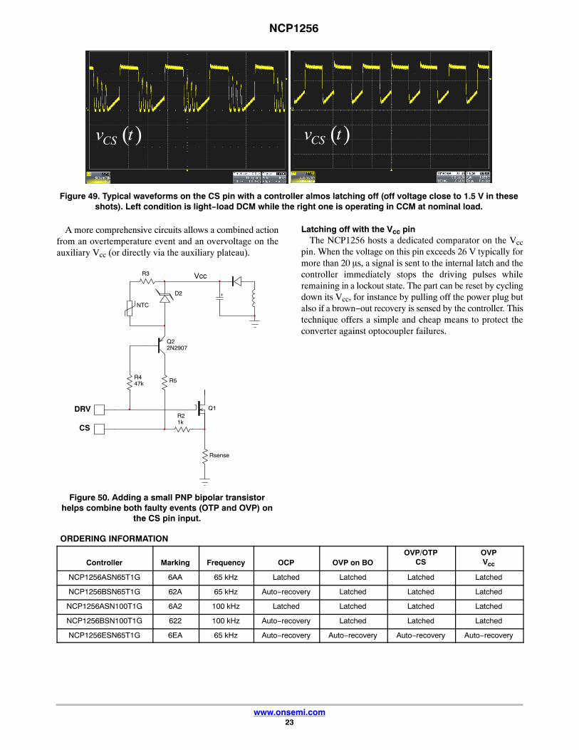
( )CSv t ( )CSv t
Figure 49. Typical waveforms on the CS pin with a controller almos latching off (off voltage close to 1.5 V in theseshots). Left condition is light−load DCM while the right one is operating in CCM at nominal load.
A more comprehensive circuits allows a combined actionfrom an overtemperature event and an overvoltage on theauxiliary Vcc (or directly via the auxiliary plateau).
Q1
Rsense
R21k
Q22N2907
D2
R3
NTC
R447k
DRV
CS
Vcc
R5
Figure 50. Adding a small PNP bipolar transistorhelps combine both faulty events (OTP and OVP) on
the CS pin input.
Latching off with the Vcc pinThe NCP1256 hosts a dedicated comparator on the Vcc
pin. When the voltage on this pin exceeds 26 V typically formore than 20 �s, a signal is sent to the internal latch and thecontroller immediately stops the driving pulses whileremaining in a lockout state. The part can be reset by cyclingdown its Vcc, for instance by pulling off the power plug butalso if a brown−out recovery is sensed by the controller. Thistechnique offers a simple and cheap means to protect theconverter against optocoupler failures.
ORDERING INFORMATION
Controller Marking Frequency OCP OVP on BOOVP/OTP
CSOVPVcc
NCP1256ASN65T1G 6AA 65 kHz Latched Latched Latched Latched
NCP1256BSN65T1G 62A 65 kHz Auto−recovery Latched Latched Latched
NCP1256ASN100T1G 6A2 100 kHz Latched Latched Latched Latched
NCP1256BSN100T1G 622 100 kHz Auto−recovery Latched Latched Latched
NCP1256ESN65T1G 6EA 65 kHz Auto−recovery Auto−recovery Auto−recovery Auto−recovery

ÉÉÉÉ
TSOP−6CASE 318G−02
ISSUE VDATE 12 JUN 2012SCALE 2:1
STYLE 1:PIN 1. DRAIN
2. DRAIN3. GATE4. SOURCE5. DRAIN6. DRAIN
2 3
456
D
1
eb
E1
A1
A0.05
NOTES:1. DIMENSIONING AND TOLERANCING PER ASME Y14.5M, 1994.2. CONTROLLING DIMENSION: MILLIMETERS.3. MAXIMUM LEAD THICKNESS INCLUDES LEAD FINISH. MINIMUM
LEAD THICKNESS IS THE MINIMUM THICKNESS OF BASE MATERIAL.4. DIMENSIONS D AND E1 DO NOT INCLUDE MOLD FLASH,
PROTRUSIONS, OR GATE BURRS. MOLD FLASH, PROTRUSIONS, ORGATE BURRS SHALL NOT EXCEED 0.15 PER SIDE. DIMENSIONS DAND E1 ARE DETERMINED AT DATUM H.
5. PIN ONE INDICATOR MUST BE LOCATED IN THE INDICATED ZONE.
c
STYLE 2:PIN 1. EMITTER 2
2. BASE 13. COLLECTOR 14. EMITTER 15. BASE 26. COLLECTOR 2
STYLE 3:PIN 1. ENABLE
2. N/C3. R BOOST4. Vz5. V in6. V out
STYLE 4:PIN 1. N/C
2. V in3. NOT USED4. GROUND5. ENABLE6. LOAD
XXX M�
�
XXX = Specific Device CodeA =Assembly LocationY = YearW = Work Week� = Pb−Free Package
STYLE 5:PIN 1. EMITTER 2
2. BASE 23. COLLECTOR 14. EMITTER 15. BASE 16. COLLECTOR 2
STYLE 6:PIN 1. COLLECTOR
2. COLLECTOR3. BASE4. EMITTER5. COLLECTOR6. COLLECTOR
STYLE 7:PIN 1. COLLECTOR
2. COLLECTOR3. BASE4. N/C5. COLLECTOR6. EMITTER
STYLE 8:PIN 1. Vbus
2. D(in)3. D(in)+4. D(out)+5. D(out)6. GND
GENERICMARKING DIAGRAM*
STYLE 9:PIN 1. LOW VOLTAGE GATE
2. DRAIN3. SOURCE4. DRAIN5. DRAIN6. HIGH VOLTAGE GATE
STYLE 10:PIN 1. D(OUT)+
2. GND3. D(OUT)−4. D(IN)−5. VBUS6. D(IN)+
1
1
*For additional information on our Pb−Free strategy and solderingdetails, please download the ON Semiconductor Soldering andMounting Techniques Reference Manual, SOLDERRM/D.
SOLDERING FOOTPRINT*
STYLE 11:PIN 1. SOURCE 1
2. DRAIN 23. DRAIN 24. SOURCE 25. GATE 16. DRAIN 1/GATE 2
STYLE 12:PIN 1. I/O
2. GROUND3. I/O4. I/O5. VCC6. I/O
*This information is generic. Please refer to device data sheetfor actual part marking. Pb−Free indicator, “G” or microdot “�”, may or may not be present.
XXXAYW�
�
1
STANDARDIC
XXX = Specific Device CodeM = Date Code� = Pb−Free Package
DIMA
MIN NOM MAXMILLIMETERS
0.90 1.00 1.10A1 0.01 0.06 0.10b 0.25 0.38 0.50c 0.10 0.18 0.26D 2.90 3.00 3.10E 2.50 2.75 3.00
e 0.85 0.95 1.05L 0.20 0.40 0.60
0.25 BSCL2−0° 10°
STYLE 13:PIN 1. GATE 1
2. SOURCE 23. GATE 24. DRAIN 25. SOURCE 16. DRAIN 1
STYLE 14:PIN 1. ANODE
2. SOURCE3. GATE4. CATHODE/DRAIN5. CATHODE/DRAIN6. CATHODE/DRAIN
STYLE 15:PIN 1. ANODE
2. SOURCE3. GATE4. DRAIN5. N/C6. CATHODE
1.30 1.50 1.70E1
E
RECOMMENDED
NOTE 5
LCM
H
L2
SEATINGPLANE
GAUGEPLANE
DETAIL Z
DETAIL Z
0.606X
3.200.956X
0.95PITCH
DIMENSIONS: MILLIMETERS
M
STYLE 16:PIN 1. ANODE/CATHODE
2. BASE3. EMITTER4. COLLECTOR5. ANODE6. CATHODE
STYLE 17:PIN 1. EMITTER
2. BASE3. ANODE/CATHODE4. ANODE5. CATHODE6. COLLECTOR
MECHANICAL CASE OUTLINE
PACKAGE DIMENSIONS
ON Semiconductor and are trademarks of Semiconductor Components Industries, LLC dba ON Semiconductor or its subsidiaries in the United States and/or other countries.ON Semiconductor reserves the right to make changes without further notice to any products herein. ON Semiconductor makes no warranty, representation or guarantee regardingthe suitability of its products for any particular purpose, nor does ON Semiconductor assume any liability arising out of the application or use of any product or circuit, and specificallydisclaims any and all liability, including without limitation special, consequential or incidental damages. ON Semiconductor does not convey any license under its patent rights nor therights of others.
98ASB14888CDOCUMENT NUMBER:
DESCRIPTION:
Electronic versions are uncontrolled except when accessed directly from the Document Repository.Printed versions are uncontrolled except when stamped “CONTROLLED COPY” in red.
PAGE 1 OF 1TSOP−6
© Semiconductor Components Industries, LLC, 2019 www.onsemi.com

onsemi, , and other names, marks, and brands are registered and/or common law trademarks of Semiconductor Components Industries, LLC dba “onsemi” or its affiliatesand/or subsidiaries in the United States and/or other countries. onsemi owns the rights to a number of patents, trademarks, copyrights, trade secrets, and other intellectual property.A listing of onsemi’s product/patent coverage may be accessed at www.onsemi.com/site/pdf/Patent−Marking.pdf. onsemi reserves the right to make changes at any time to anyproducts or information herein, without notice. The information herein is provided “as−is” and onsemi makes no warranty, representation or guarantee regarding the accuracy of theinformation, product features, availability, functionality, or suitability of its products for any particular purpose, nor does onsemi assume any liability arising out of the application or useof any product or circuit, and specifically disclaims any and all liability, including without limitation special, consequential or incidental damages. Buyer is responsible for its productsand applications using onsemi products, including compliance with all laws, regulations and safety requirements or standards, regardless of any support or applications informationprovided by onsemi. “Typical” parameters which may be provided in onsemi data sheets and/or specifications can and do vary in different applications and actual performance mayvary over time. All operating parameters, including “Typicals” must be validated for each customer application by customer’s technical experts. onsemi does not convey any licenseunder any of its intellectual property rights nor the rights of others. onsemi products are not designed, intended, or authorized for use as a critical component in life support systemsor any FDA Class 3 medical devices or medical devices with a same or similar classification in a foreign jurisdiction or any devices intended for implantation in the human body. ShouldBuyer purchase or use onsemi products for any such unintended or unauthorized application, Buyer shall indemnify and hold onsemi and its officers, employees, subsidiaries, affiliates,and distributors harmless against all claims, costs, damages, and expenses, and reasonable attorney fees arising out of, directly or indirectly, any claim of personal injury or deathassociated with such unintended or unauthorized use, even if such claim alleges that onsemi was negligent regarding the design or manufacture of the part. onsemi is an EqualOpportunity/Affirmative Action Employer. This literature is subject to all applicable copyright laws and is not for resale in any manner.
PUBLICATION ORDERING INFORMATIONTECHNICAL SUPPORTNorth American Technical Support:Voice Mail: 1 800−282−9855 Toll Free USA/CanadaPhone: 011 421 33 790 2910
LITERATURE FULFILLMENT:Email Requests to: [email protected]
onsemi Website: www.onsemi.com
Europe, Middle East and Africa Technical Support:Phone: 00421 33 790 2910For additional information, please contact your local Sales Representative
◊