Embed Size (px)
Citation preview
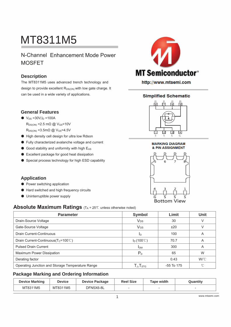
MT8311M5 MT8311M5
The MT8311M5 uses advanced trench technology and
MOSFET Enhancement Mode Power N-Channel
Description
design to provide excellent RDS(ON) with low gate charge. It
can be used in a wide variety of applications.
General Features VDS =30V,ID =100A
RDS(ON) <2.5 m @ VGS=10V
RDS(ON) <3.5m @ VGS=4.5V
High density cell design for ultra low Rdson
Fully characterized avalanche voltage and current
Good stability and uniformity with high EAS
Excellent package for good heat dissipation
Special process technology for high ESD capability
Application Power switching application
Hard switched and high frequency circuits
Uninterruptible power supply
Parameter Symbol Limit Unit Drain-Source Voltage VDS 30 V
Gate-Source Voltage VGS ±20 V
Drain Current-Continuous ID 100 A
Drain Current-Continuous(TC=100 ) ID (100 ) 70.7 A
Pulsed Drain Current IDM 300 A
Maximum Power Dissipation PD 65 W
Derating factor 0.43 W/
Operating Junction and Storage Temperature Range TJ,TSTG -55 To 175
1
Package Marking and Ordering Information Device Marking Device Device Package Reel Size Tape width Quantity
DFN5X6-8L - - -
MT8311M5
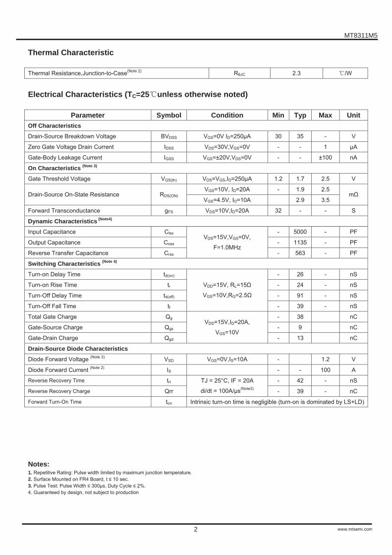
Thermal Characteristic Thermal Resistance,Junction-to-Case(Note 2) R JC 2.3 /W
Electrical Characteristics (TC=25 unless otherwise noted)
Parameter Symbol Condition Min Typ Max Unit Off Characteristics
Drain-Source Breakdown Voltage BVDSS VGS=0V ID=250 A 30 35 - V
Zero Gate Voltage Drain Current IDSS VDS=30V,VGS=0V - - 1 A
Gate-Body Leakage Current IGSS VGS=±20V,VDS=0V - - ±100 nA
On Characteristics (Note 3)
Gate Threshold Voltage VGS(th) VDS=VGS,ID=250 A 1.2 1.7 2.5 V
VGS=10V, ID=20A - 1.9 2.5 Drain-Source On-State Resistance RDS(ON)
VGS=4.5V, ID=10A 2.9 3.5 m
Forward Transconductance gFS VDS=10V,ID=20A 32 - - S
Dynamic Characteristics (Note4)
Input Capacitance Clss - 5000 - PF
Output Capacitance Coss - 1135 - PF
Reverse Transfer Capacitance Crss
VDS=15V,VGS=0V,
F=1.0MHz - 563 - PF
Switching Characteristics (Note 4)
Turn-on Delay Time td(on) - 26 - nS
Turn-on Rise Time tr - 24 - nS
Turn-Off Delay Time td(off) - 91 - nS
Turn-Off Fall Time tf
VDD=15V, RL=15
VGS=10V,RG=2.5
- 39 - nS
Total Gate Charge Qg - 38 nC
Gate-Source Charge Qgs - 9 nC
Gate-Drain Charge Qgd
VDS=15V,ID=20A,
VGS=10V - 13 nC
Drain-Source Diode Characteristics
Diode Forward Voltage (Note 3) VSD VGS=0V,IS=10A - 1.2 V
Diode Forward Current (Note 2) IS - - 100 A
Reverse Recovery Time trr - 42 - nS
Reverse Recovery Charge Qrr
TJ = 25°C, IF = 20A
di/dt = 100A/ s(Note3) - 39 - nC
Forward Turn-On Time ton Intrinsic turn-on time is negligible (turn-on is dominated by LS+LD)
Notes: 1. Repetitive Rating: Pulse width limited by maximum junction temperature. 2. Surface Mounted on FR4 Board, t 10 sec. 3. Pulse Test: Pulse Width 300 s, Duty Cycle 2%. 4. Guaranteed by design, not subject to production
MT8311M5
2
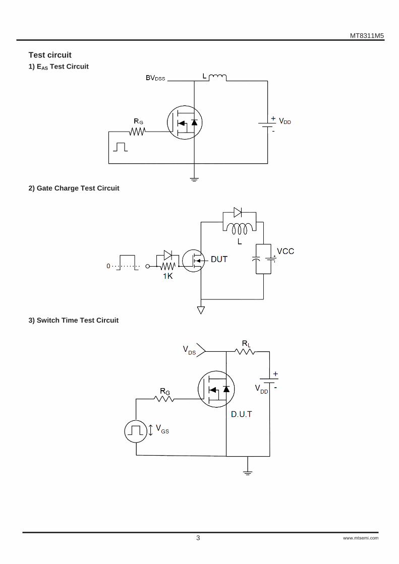
Test circuit 1) EAS Test Circuit
2) Gate Charge Test Circuit
3) Switch Time Test Circuit
MT8311M5
3
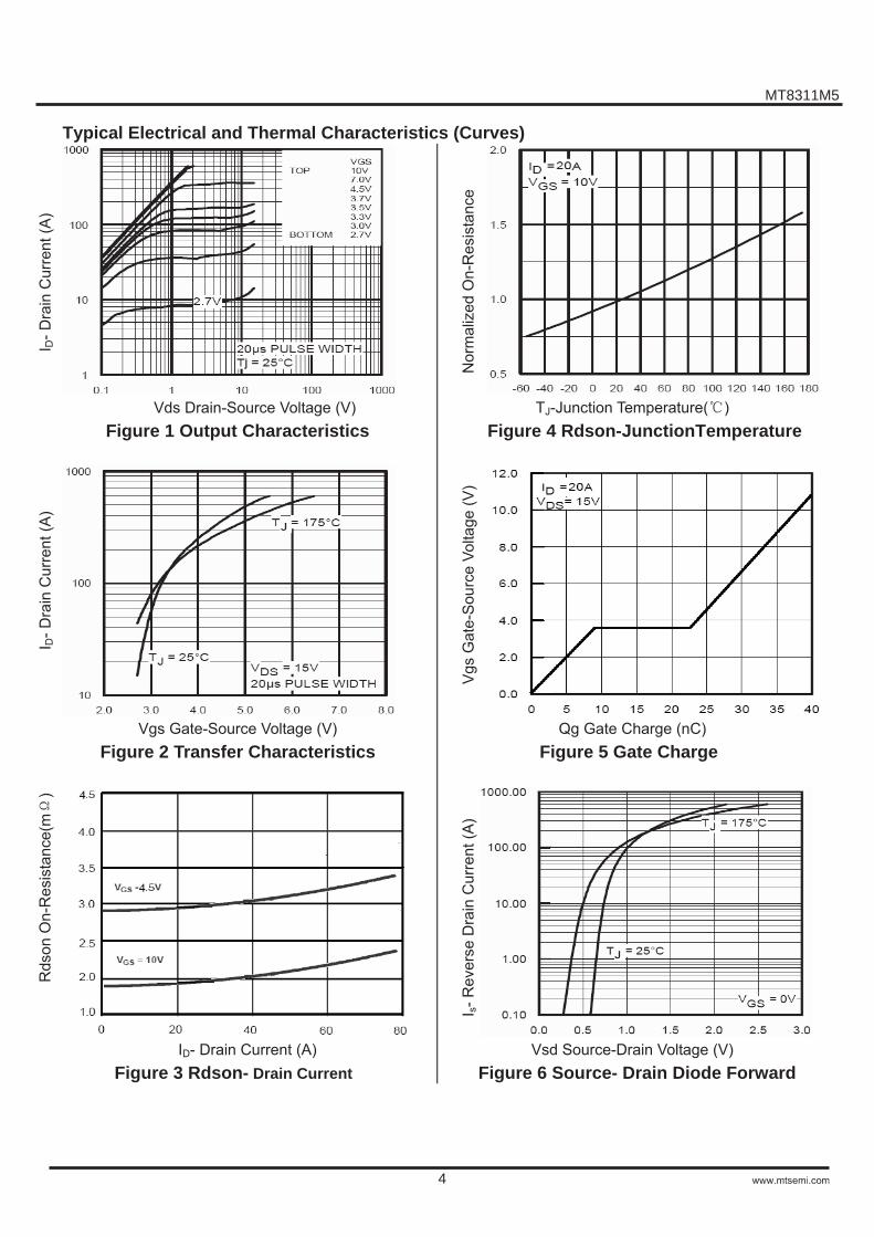
Typical Electrical and Thermal Characteristics (Curves)
Vds Drain-Source Voltage (V)
Figure 1 Output Characteristics
Vgs Gate-Source Voltage (V)
Figure 2 Transfer Characteristics
ID- Drain Current (A)
Figure 3 Rdson- Drain Current
TJ-Junction Temperature( )
Figure 4 Rdson-JunctionTemperature
Qg Gate Charge (nC)
Figure 5 Gate Charge
Vsd Source-Drain Voltage (V)
Figure 6 Source- Drain Diode Forward
Rds
on O
n-R
esis
tanc
e(m
) I D
- Dra
in C
urre
nt (A
) I D
- Dra
in C
urre
nt (A
)
Nor
mal
ized
On-
Res
ista
nce
Vgs
Gat
e-S
ourc
e Vo
ltage
(V)
I s- R
ever
se D
rain
Cur
rent
(A)
MT8311M5
4

Vds Drain-Source Voltage (V) Figure 7 Capacitance vs Vds
Vds Drain-Source Voltage (V)
Figure 8 Safe Operation Area
TJ-Junction Temperature( )
Figure 9 BVDSS vs Junction Temperature
TJ-Junction Temperature( )
Figure 10 VGS(th) vs Junction Temperature
I D- D
rain
Cur
rent
(A)
C C
apac
itanc
e (p
F)
Square Wave Pluse Duration(sec) Figure 11 Normalized Maximum Transient Thermal Impedance
r(t),
Nor
mal
ized
Effe
ctiv
e Tr
ansi
ent T
herm
al Im
peda
nce
MT8311M5
5
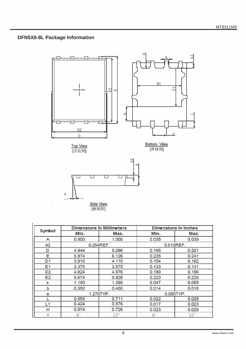
DFN5X6-8L Package Information
MT8311M5
6