Embed Size (px)
Citation preview
QPA9122 2.3 – 5.0 GHz 0.5 W Driver Amplifier
Data Sheet, May 14, 2020 | Subject to change without notice 1 of 12 www.qorvo.com
®
16 Pad 3 x 3 mm Laminate Package
Key Features • 2.3 – 5.0 GHz Operational Frequency
• 50Ω Matched RF Input and Output
• +27 dBm P3dB
• 36.0 dB Gain at 2.6 GHz
• +5 V Single Supply, ICQ 95 mA
• DC Power Shutdown Feature
Product Overview The QPA9122 is a wideband, high gain, and high peak
power driver amplifier. It provides 36dB gain at 2.6GHz and
achieves a peak power of 27dBm P3dB. With a quiescent
current of 95mA, the amplifier can provide good DPD
linearity performance with wideband signals of up to
160 MHz IBW making it perfectly suited for m-MIMO
applications.
The QPA9122 is internally match to 50Ω over the entire
operating frequency band of 2.3 – 5.0 GHz and
incorporates a shut-down function through the VPD pin.
The QPA9122 is housed in a 16-pin 3X3mm SMT package
and is footprint and pin-compatible to QPA9120 and
QPA9121.
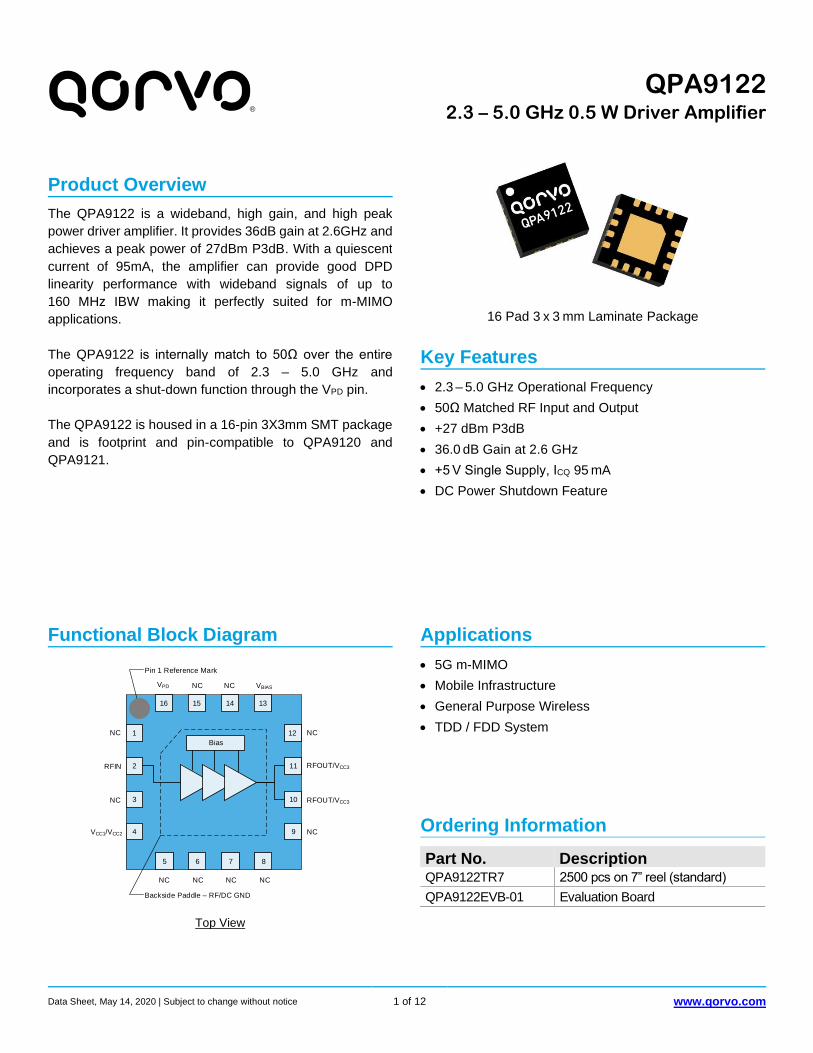
Functional Block Diagram
NC 1
2
3
4
8765
12
11
10
9
13141516
Bias
NC
NC NC NC NC
RFIN
VCC1/VCC2
VPD
RFOUT/VCC3
NC
NC
NC NC VBIAS
RFOUT/VCC3
Backside Paddle – RF/DC GND
Pin 1 Reference Mark
Top View
Applications • 5G m-MIMO
• Mobile Infrastructure
• General Purpose Wireless
• TDD / FDD System
Ordering Information
Part No. Description QPA9122TR7 2500 pcs on 7” reel (standard)
QPA9122EVB-01 Evaluation Board
QPA9122
2.3 – 5.0 GHz 0.5 W Driver Amplifier
Data Sheet, May 14, 2020 | Subject to change without notice 2 of 12 www.qorvo.com
®
Recommended Operating Conditions Parameter Min Typ Max Units
Supply Voltage (VCC) +4.75 +5 +5.25 V
TCASE -40 +105 °C
Tj for >106 hours MTTF +218 °C
Electrical specifications are measured at specified test conditions. Specifications are not guaranteed over all recommended operating conditions. Operating the part above the maximum recommended Tcase may degrade performance.
Absolute Maximum Ratings Parameter Rating
Storage Temperature -65 to +150°C
TCASE -40 to +125°C
RF Input Power, ON state, CW, T=25 °C,
2:1 VSWR, In-band +10 dBm
RF Input Power, OFF state, CW, T=25 °C,
2:1 VSWR, In-band +10 dBm
Device Voltage (VCC1) +6 V
Exceeding any one or a combination of the Absolute Maximum Rating conditions may cause permanent damage to the device. Extended application of Absolute Maximum Rating conditions to the device may reduce device reliability.
Electrical Specifications Parameter Conditions (1) Min Typ Max Units
Operational Frequency Range 2300 5000 MHz
Gain At 2.6 GHz 33.7 36 39.7 dB
At 3.6 GHz 34 36.5 40 dB
Gain Flatness Any 100 MHz BW within band 0.8 dB
Input Return Loss 15 dB
Output Return Loss 12 dB
Reverse Isolation ON state 50 dB
Forward Isolation OFF state 45 dB
Output P1dB At 2.6 GHz 24.5 25.3 dBm
At 3.6 GHz 25 26 dBm
Output P3dB At 2.6 GHz 25.5 26.9 dBm
At 3.6 GHz 25.5 27 dBm
ACPR
At 2.6 GHz, Pout=+15 dBm, 1C LTE 20MHz, 8dB PAR
-45.7 -38 dBc
At 3.6 GHz, Pout=+15 dBm, 1C LTE 20MHz, 8dB PAR
-39.5 -34 dBc
Noise Figure At 3.6 GHz 5.3 dB
Device Current, ON ICQ Quiescent Current 50 95 125 mA
Device Current, OFF VPD = 0 V 2 µA
VPD, Logic Low 0 0.63 V
VPD, Logic High 1.17 VCC V
Device ON or OFF Timing 50% Ctrl to 10/90% RF 0.45 µS
Thermal Resistance, θjc Junction to case 65 °C/W
Notes: 1. Test conditions unless otherwise noted: VCC = +5.0 V, VPD = +1.8 V, Temp = +25 °C, 50 Ω system.
QPA9122
2.3 – 5.0 GHz 0.5 W Driver Amplifier
Data Sheet, May 14, 2020 | Subject to change without notice 3 of 12 www.qorvo.com
®
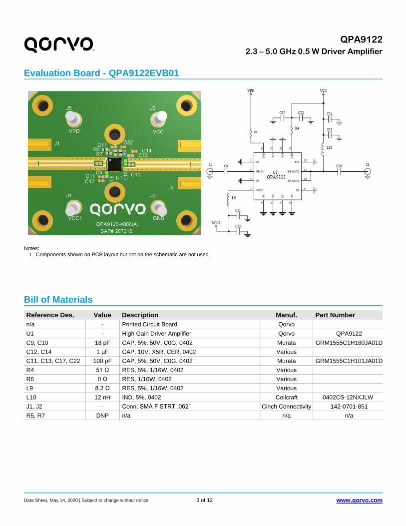
Evaluation Board - QPA9122EVB01
Notes: 1. Components shown on PCB layout but not on the schematic are not used.
Bill of Materials Reference Des. Value Description Manuf. Part Number
n/a - Printed Circuit Board Qorvo
U1 - High Gain Driver Amplifier Qorvo QPA9122
C9, C10 18 pF CAP, 5%, 50V, C0G, 0402 Murata GRM1555C1H180JA01D
C12, C14 1 µF CAP, 10V, X5R, CER, 0402 Various
C11, C13, C17, C22 100 pF CAP, 5%, 50V, C0G, 0402 Murata GRM1555C1H101JA01D
R4 51 Ω RES, 5%, 1/16W, 0402 Various
R6 0 Ω RES, 1/10W, 0402 Various
L9 8.2 Ω RES, 5%, 1/16W, 0402 Various
L10 12 nH IND, 5%, 0402 Coilcraft 0402CS-12NXJLW
J1, J2 - Conn, SMA F STRT .062” Cinch Connectivity 142-0701-851
R5, R7 DNP n/a n/a n/a

QPA9122
2.3 – 5.0 GHz 0.5 W Driver Amplifier
Data Sheet, May 14, 2020 | Subject to change without notice 4 of 12 www.qorvo.com
®
Logic Table
Parameter, VPD High Low
Device State ON OFF
Typical Performance
Parameter Conditions Typical Value Units
Frequency 2600 3600 4900 MHz
Gain 36.8 36 34 dB
Input Return Loss 16.6 16.7 18.9 dB
Output Return Loss 17.4 18.1 13.3 dB
Output P3dB 26.9 27.2 26.8 dBm
Output IP3 Pout = +0 dBm/tone, f = 1 MHz 32.4 32.9 30.0 dBm
ACPR Pout=+15 dBm, 1C LTE, 20MHz, 8.5dB PAR -46.1 -40.7 -38.1 dBc
Device Current VCC and VCC1 combined 95 mA
Notes: 1. Test Conditions unless otherwise noted: VCC and VCC1 on EVB = +5.0 V, ICC = 95 mA, VPD = +1.8 V, Temp.=+25 °C
QPA9122
2.3 – 5.0 GHz 0.5 W Driver Amplifier
Data Sheet, May 14, 2020 | Subject to change without notice 5 of 12 www.qorvo.com
®
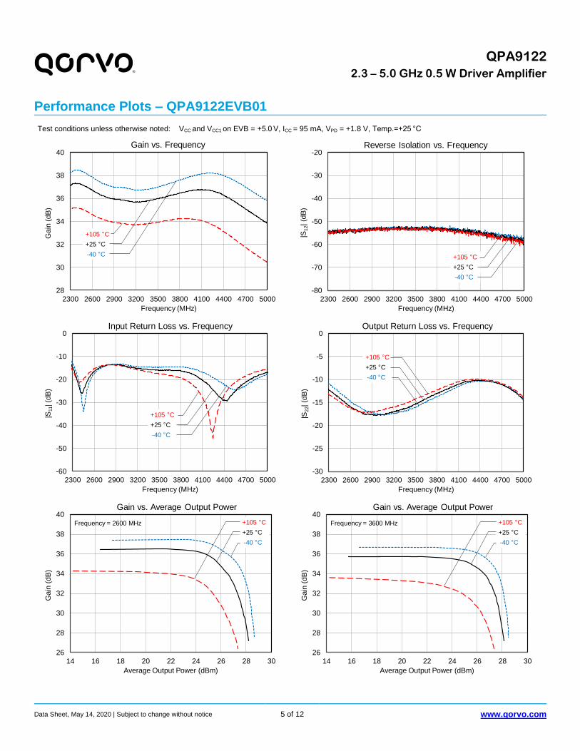
Performance Plots – QPA9122EVB01
Test conditions unless otherwise noted: VCC and VCC1 on EVB = +5.0 V, ICC = 95 mA, VPD = +1.8 V, Temp.=+25 °C
28
30
32
34
36
38
40
2300 2600 2900 3200 3500 3800 4100 4400 4700 5000
Ga
in (
dB
)
Frequency (MHz)
Gain vs. Frequency
+105 °C
+25 °C
-40 °C
-80
-70
-60
-50
-40
-30
-20
2300 2600 2900 3200 3500 3800 4100 4400 4700 5000|S
12| (d
B)
Frequency (MHz)
Reverse Isolation vs. Frequency
+105 °C
+25 °C
-40 °C
-60
-50
-40
-30
-20
-10
0
2300 2600 2900 3200 3500 3800 4100 4400 4700 5000
|S11| (d
B)
Frequency (MHz)
Input Return Loss vs. Frequency
+105 °C
+25 °C
-40 °C
-30
-25
-20
-15
-10
-5
0
2300 2600 2900 3200 3500 3800 4100 4400 4700 5000
|S22| (d
B)
Frequency (MHz)
Output Return Loss vs. Frequency
+105 °C
+25 °C
-40 °C
26
28
30
32
34
36
38
40
14 16 18 20 22 24 26 28 30
Ga
in (
dB
)
Average Output Power (dBm)
Gain vs. Average Output Power
+105 °C
+25 °C
-40 °C
Frequency = 2600 MHz
26
28
30
32
34
36
38
40
14 16 18 20 22 24 26 28 30
Ga
in (
dB
)
Average Output Power (dBm)
Gain vs. Average Output Power
+105 °C
+25 °C
-40 °C
Frequency = 3600 MHz
QPA9122
2.3 – 5.0 GHz 0.5 W Driver Amplifier
Data Sheet, May 14, 2020 | Subject to change without notice 6 of 12 www.qorvo.com
®
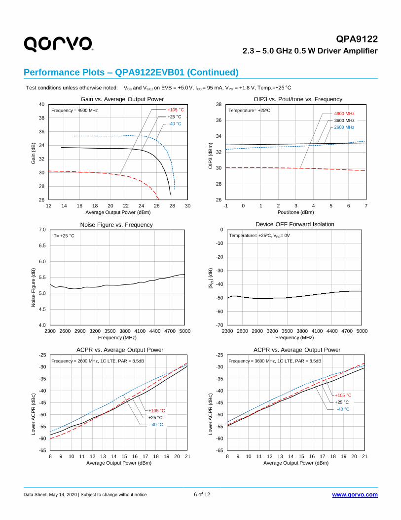
Performance Plots – QPA9122EVB01 (Continued)
Test conditions unless otherwise noted: VCC and VCC1 on EVB = +5.0 V, ICC = 95 mA, VPD = +1.8 V, Temp.=+25 °C
26
28
30
32
34
36
38
40
12 14 16 18 20 22 24 26 28 30
Ga
in (
dB
)
Average Output Power (dBm)
Gain vs. Average Output Power
+105 °C
+25 °C
-40 °C
Frequency = 4900 MHz
26
28
30
32
34
36
38
-1 0 1 2 3 4 5 6 7O
IP3
(d
Bm
)Pout/tone (dBm)
OIP3 vs. Pout/tone vs. Frequency
Temperature= +25ºC4900 MHz
3600 MHz
2600 MHz
4.0
4.5
5.0
5.5
6.0
6.5
7.0
2300 2600 2900 3200 3500 3800 4100 4400 4700 5000
No
ise
Fig
ure
(d
B)
Frequency (MHz)
Noise Figure vs. Frequency
T= +25 °C
-70
-60
-50
-40
-30
-20
-10
0
2300 2600 2900 3200 3500 3800 4100 4400 4700 5000
|S21| (d
B)
Frequency (MHz)
Device OFF Forward Isolation
Temperature= +25ºC, VPD= 0V
-65
-60
-55
-50
-45
-40
-35
-30
-25
8 9 10 11 12 13 14 15 16 17 18 19 20 21
Lo
we
r A
CP
R (d
Bc)
Average Output Power (dBm)
ACPR vs. Average Output Power
+105 °C
+25 °C
-40 °C
Frequency = 2600 MHz, 1C LTE, PAR = 8.5dB
-65
-60
-55
-50
-45
-40
-35
-30
-25
8 9 10 11 12 13 14 15 16 17 18 19 20 21
Lo
we
r A
CP
R (d
Bc)
Average Output Power (dBm)
ACPR vs. Average Output Power
+105 °C
+25 °C
-40 °C
Frequency = 3600 MHz, 1C LTE, PAR = 8.5dB
QPA9122
2.3 – 5.0 GHz 0.5 W Driver Amplifier
Data Sheet, May 14, 2020 | Subject to change without notice 7 of 12 www.qorvo.com
®
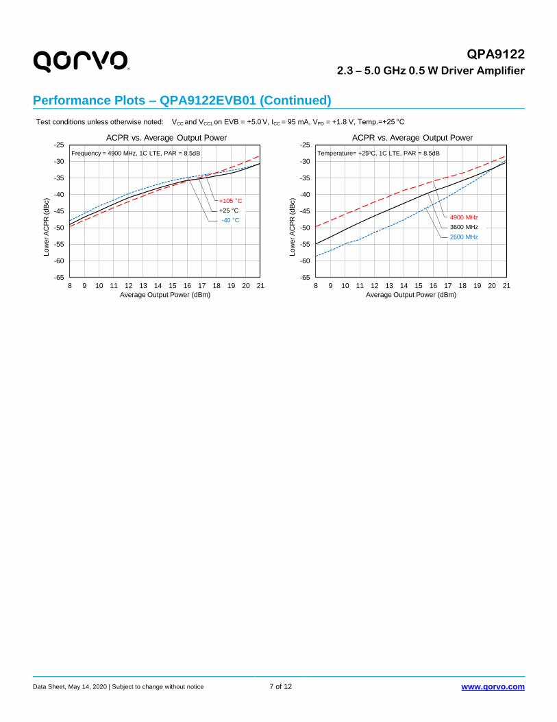
Performance Plots – QPA9122EVB01 (Continued)
Test conditions unless otherwise noted: VCC and VCC1 on EVB = +5.0 V, ICC = 95 mA, VPD = +1.8 V, Temp.=+25 °C
-65
-60
-55
-50
-45
-40
-35
-30
-25
8 9 10 11 12 13 14 15 16 17 18 19 20 21
Lo
we
r A
CP
R (d
Bc)
Average Output Power (dBm)
ACPR vs. Average Output Power
+105 °C
+25 °C
-40 °C
Frequency = 4900 MHz, 1C LTE, PAR = 8.5dB
-65
-60
-55
-50
-45
-40
-35
-30
-25
8 9 10 11 12 13 14 15 16 17 18 19 20 21L
ow
er A
CP
R (d
Bc)
Average Output Power (dBm)
ACPR vs. Average Output Power
4900 MHz
3600 MHz
2600 MHz
Temperature= +25ºC, 1C LTE, PAR = 8.5dB
QPA9122
2.3 – 5.0 GHz 0.5 W Driver Amplifier
Data Sheet, May 14, 2020 | Subject to change without notice 8 of 12 www.qorvo.com
®
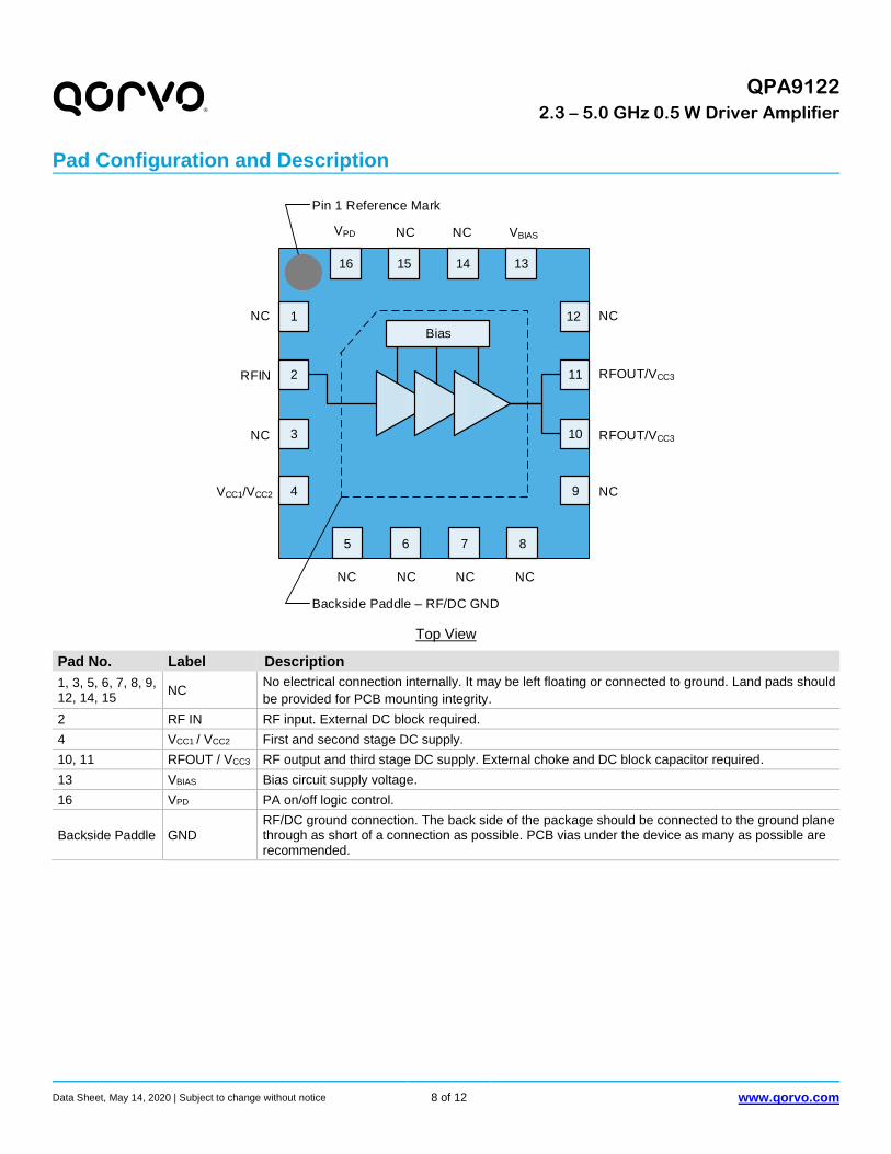
Pad Configuration and Description
NC 1
2
3
4
8765
12
11
10
9
13141516
Bias
NC
NC NC NC NC
RFIN
VCC1/VCC2
VPD
RFOUT/VCC3
NC
NC
NC NC VBIAS
RFOUT/VCC3
Backside Paddle – RF/DC GND
Pin 1 Reference Mark
Top View
Pad No. Label Description
1, 3, 5, 6, 7, 8, 9, 12, 14, 15
NC No electrical connection internally. It may be left floating or connected to ground. Land pads should
be provided for PCB mounting integrity.
2 RF IN RF input. External DC block required.
4 VCC1 / VCC2 First and second stage DC supply.
10, 11 RFOUT / VCC3 RF output and third stage DC supply. External choke and DC block capacitor required.
13 VBIAS Bias circuit supply voltage.
16 VPD PA on/off logic control.
Backside Paddle GND RF/DC ground connection. The back side of the package should be connected to the ground plane through as short of a connection as possible. PCB vias under the device as many as possible are recommended.
QPA9122
2.3 – 5.0 GHz 0.5 W Driver Amplifier
Data Sheet, May 14, 2020 | Subject to change without notice 9 of 12 www.qorvo.com
®
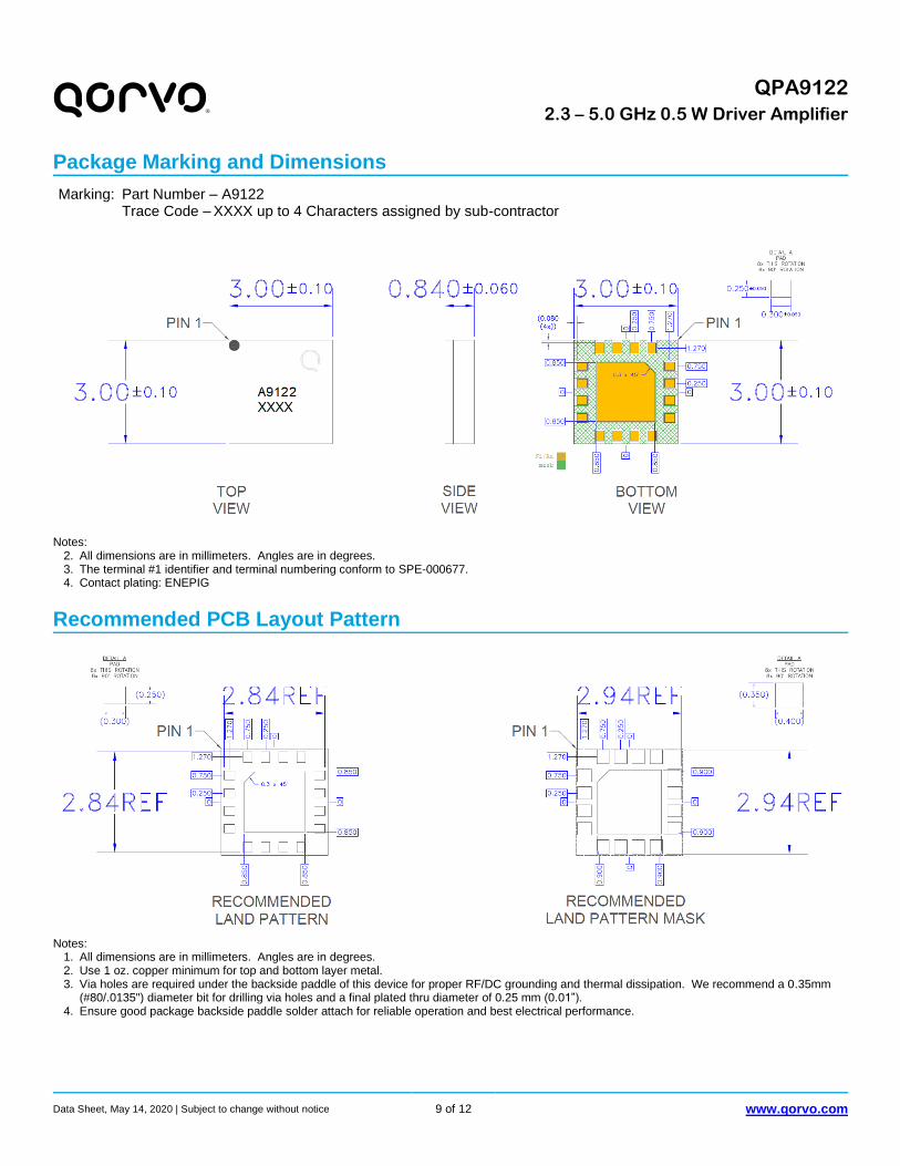
Recommended PCB Layout Pattern
Notes:
1. All dimensions are in millimeters. Angles are in degrees. 2. Use 1 oz. copper minimum for top and bottom layer metal. 3. Via holes are required under the backside paddle of this device for proper RF/DC grounding and thermal dissipation. We recommend a 0.35mm
(#80/.0135") diameter bit for drilling via holes and a final plated thru diameter of 0.25 mm (0.01”). 4. Ensure good package backside paddle solder attach for reliable operation and best electrical performance.
Package Marking and Dimensions
Marking: Part Number – A9122 Trace Code – XXXX up to 4 Characters assigned by sub-contractor
Notes: 2. All dimensions are in millimeters. Angles are in degrees. 3. The terminal #1 identifier and terminal numbering conform to SPE-000677. 4. Contact plating: ENEPIG

QPA9122
2.3 – 5.0 GHz 0.5 W Driver Amplifier
Data Sheet, May 14, 2020 | Subject to change without notice 10 of 12 www.qorvo.com
®
Tape and Reel Information – Carrier and Cover Tape Dimensions
Feature Measure Symbol Size (in) Size (mm)
Cavity
Length A0 0.128 3.25
Width B0 0.128 3.25
Depth K0 0.055 1.40
Pitch P1 0.157 4.00
Centerline Distance Cavity to Perforation - Length Direction P2 0.079 2.00
Cavity to Perforation - Width Direction F 0.217 5.50
Cover Tape Width C 0.362 9.20
Carrier Tape Width W 0.472 12.00
QPA9122
2.3 – 5.0 GHz 0.5 W Driver Amplifier
Data Sheet, May 14, 2020 | Subject to change without notice 11 of 12 www.qorvo.com
®
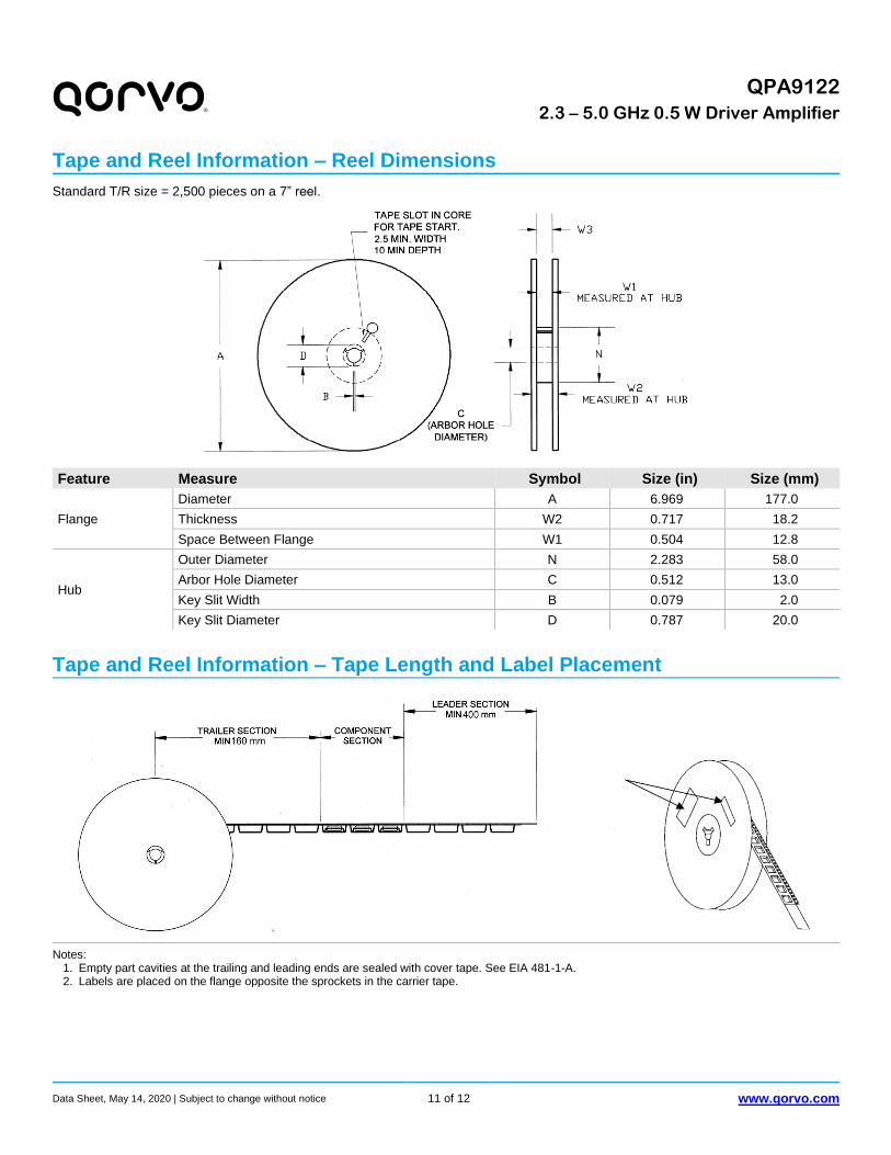
Tape and Reel Information – Reel Dimensions
Standard T/R size = 2,500 pieces on a 7” reel.
Feature Measure Symbol Size (in) Size (mm)
Flange
Diameter A 6.969 177.0
Thickness W2 0.717 18.2
Space Between Flange W1 0.504 12.8
Hub
Outer Diameter N 2.283 58.0
Arbor Hole Diameter C 0.512 13.0
Key Slit Width B 0.079 2.0
Key Slit Diameter D 0.787 20.0
Tape and Reel Information – Tape Length and Label Placement
Notes: 1. Empty part cavities at the trailing and leading ends are sealed with cover tape. See EIA 481-1-A. 2. Labels are placed on the flange opposite the sprockets in the carrier tape.
QPA9122
2.3 – 5.0 GHz 0.5 W Driver Amplifier
Data Sheet, May 14, 2020 | Subject to change without notice 12 of 12 www.qorvo.com
®
Notes: 5. All dimensions are in millimeters. Angles are in degrees. 6. Use 1 oz. copper minimum for top and bottom layer metal. 7. Via holes are required under the backside paddle of this device for proper RF/DC grounding and thermal dissipation. We recommend a 0.35mm
(#80/.0135") diameter bit for drilling via holes and a final plated thru diameter of 0.25 mm (0.01”). 8. Ensure good package backside paddle solder attach for reliable operation and best electrical performance.
Handling Precautions Parameter Rating Standard
Caution! ESD-Sensitive Device
ESD – Human Body Model (HBM) 1C ESDA / JEDEC JS-001-2017
ESD – Charged Device Model (CDM) C3 JEDEC JESD22-C101F
MSL – Moisture Sensitivity Level MSL3 IPC/JEDEC J-STD-020
Solderability Compatible with both lead-free (260°C max. reflow temperature) and tin/lead (245°C max. reflow temperature) soldering processes.
Solder profiles available upon request.
Contact plating: ENEPIG
RoHS Compliance This part is compliant with 2011/65/EU RoHS directive (Restrictions on the Use of Certain Hazardous Substances in Electrical and Electronic Equipment) as amended by Directive 2015/863/EU. This product also has the following attributes:
• Product uses RoHS Exemption 7c-I to meet RoHS Compliance requirements
• Halogen Free (Chlorine, Bromine)
• Antimony Free
• TBBP-A (C15H12Br402) Free
• PFOS Free
• SVHC Free
Important Notice The information contained herein is believed to be reliable; however, Qorvo makes no warranties regarding the information contained herein and assumes no responsibility or liability whatsoever for the use of the information contained herein. All information contained herein is subject to change without notice. Customers should obtain and verify the latest relevant information before placing orders for Qorvo products. The information contained herein or any use of such information does not grant, explicitly or implicitly, to any party any patent rights, licenses, or any other intellectual property rights, whether with regard to such information itself or anything described by such information. THIS INFORMATION DOES NOT CONSTITUTE A WARRANTY WITH RESPECT TO THE PRODUCTS DESCRIBED HEREIN, AND QORVO HEREBY DISCLAIMS ANY AND ALL WARRANTIES WITH RESPECT TO SUCH PRODUCTS WHETHER EXPRESS OR IMPLIED BY LAW, COURSE OF DEALING, COURSE OF PERFORMANCE, USAGE OF TRADE OR OTHERWISE, INCLUDING THE IMPLIED WARRANTIES OF MERCHANTABILITY AND FITNESS FOR A PARTICULAR PURPOSE.
Without limiting the generality of the foregoing, Qorvo products are not warranted or authorized for use as critical components in medical, life-saving, or life-sustaining applications, or other applications where a failure would reasonably be expected to cause severe personal injury or death.
Copyright 2020 © Qorvo, Inc. | Qorvo is a registered trademark of Qorvo, Inc.
Contact Information For the latest specifications, additional product information, worldwide sales and distribution locations:
Web: www.qorvo.com
Tel: 1-844-890-8163
Email: [email protected]