Embed Size (px)
Citation preview
1
Navigating the PCB Surface Finish MazeSMTA - Oregon
Date: 18 May 2011
Darren Hitchcock
Field Applications Engineer
2CONFIDENTIAL | Copyright ©2011 Multek. All rights reserved. |
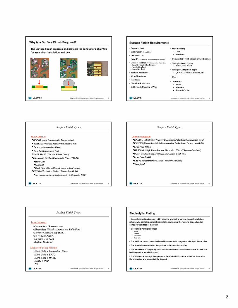
Navigating the Surface Finish Maze…
3CONFIDENTIAL | Copyright ©2011 Multek. All rights reserved. |
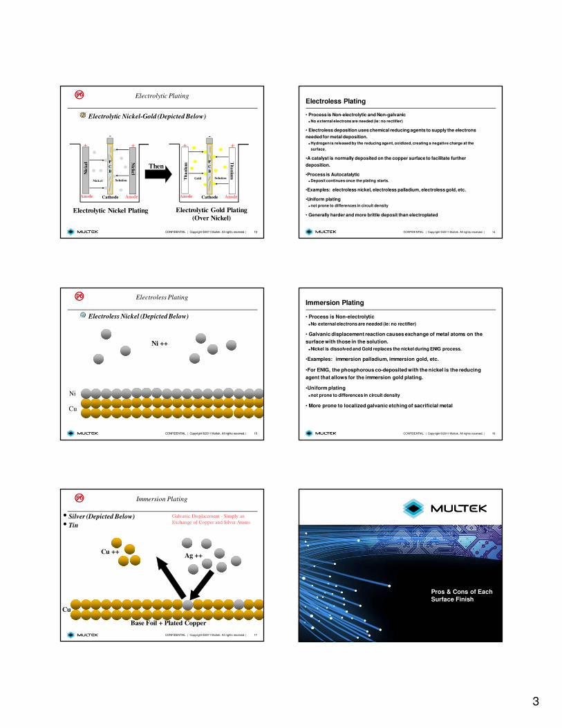
Navigating the Surface Finish Maze…
Electroless Nickel / Electroless Gold (ENEG)Direct Immersion Gold (DIG)
4CONFIDENTIAL | Copyright ©2011 Multek. All rights reserved. |
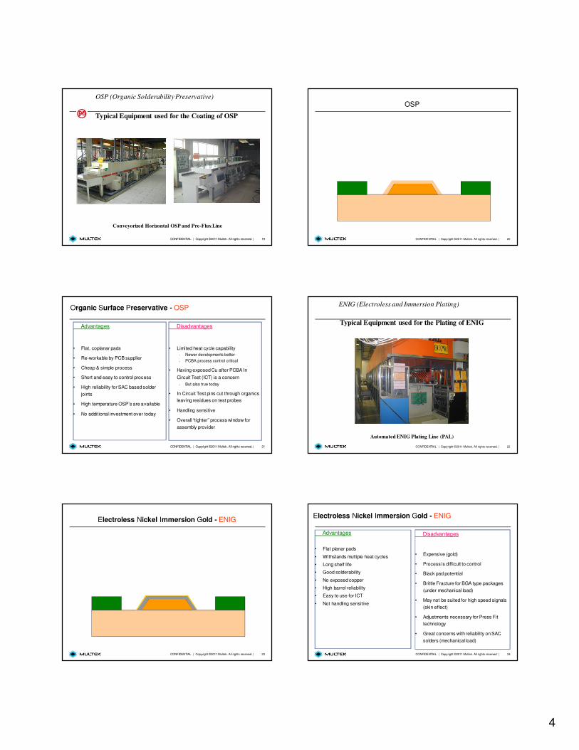
Business Overview: Global Presence
GERMANYRigid PCB Manufacturing
110 K sq ftHeadcount: 450
BRAZILRigid PCB Manufacturing
100 K sq ftHeadcount: 250
MINNESOTAFPC Manufacturing ITO & Materials Manufacturing
325 K sq ft
Headcount: 350
CHINA - ZhuhaiRigid PCB Manufacturing
FPC & Rigid Flex Manufacturing
1340 K Sq fHeadcount: 9,100
CHINA - ShenzhenLCD Displays and
Touch Sensor Manufacturing291 K Sq ft
Headcount: 2,900
We are the only PCB Shop that has Global Footprint in 4 continents
Over 13,000 people world wide, ~ 12,000 in China
5CONFIDENTIAL | Copyright ©2011 Multek. All rights reserved. |
What is a Surface Finish?
A plating or coating applied to the exposed copper features of a
Printed Wiring Board (PWB).
�Plating (metallic)
�Coating (metallic or organic)
Note: (Base) Metal Plating is typically copper (in most cases).
But for some Nickel or Nickel-Phosphorous serve as the solderable surface.
Metal Plating
Finish
Surface
6CONFIDENTIAL | Copyright ©2011 Multek. All rights reserved. |
How is the Surface Finish Applied?
�Coating
� OSP, HASL, Carbon etc.
�Plating (metallic)
� Electrolytic
� Electroless
� Immersion
�Equipment
� Horizontal or Vertical equipment
� Automated or Manual
Horizontal
Vertical
2
7CONFIDENTIAL | Copyright ©2011 Multek. All rights reserved. |
Why is a Surface Finish Required?
The Surface Finish prepares and protects the conductors of a PWB
for assembly, installation, and use.
8CONFIDENTIAL | Copyright ©2011 Multek. All rights reserved. |
• Coplanar (flat)
• Solderability (wetability)
• In Circuit Test
• Lead-Free (RoHS and WEEE compatible and compliant)
• Contact Resistance (Compression Connection)�Daughter Card Edge Fingers�Fuzz Button Pads�Grounding Rails
• Tarnish Resistance
• Wear Resistance
• Hardness
• Chemical Resistance
• Soldermask Plugging of Vias
Surface Finish Requirements
• Wire Bonding
� Gold
� Aluminum
• Compatibility with other Surface Finishes
• Multiple Solder Cycles� Reflow, Wave, Rework
• Multiple Component Types
� QFP, BGA, Passives, Press Fit, etc.
• Cost
• Reliability
� Shock
� Vibration
� Thermal Cycling
9CONFIDENTIAL | Copyright ©2011 Multek. All rights reserved. |
Surface Finish Types
Most Common:
•OSP (Organic Solderability Preservative)
• ENIG (Electroless Nickel/Immersion Gold)
• Imm Ag (Immersion Silver)
• Imm Sn (Immersion Tin)
•Sn-Pb HASL (Hot Air Solder Level)
•Electrolytic Ni /Au (Electrolytic Nickel / Gold)
•Hard Gold
•Soft Gold
•Flash Gold (thin, solderable – may be hard or soft)
•ENEG (Electroless Nickel / Electroless Gold)
•more common for packaging industry (chip carrier PWB)
10CONFIDENTIAL | Copyright ©2011 Multek. All rights reserved. |
Surface Finish Types
Under Investigation:
•ENEPIG (Electroless Nickel / Electroless Palladium / Immersion Gold)
•ENIPIG (Electroless Nickel / Immersion Palladium / Immersion Gold)
•Lead Free HASL
•HP ENIG (High Phosphorous Electroless Nickel / Immersion Gold)
•Direct Gold on Copper (Direct Immersion Gold, etc.)
•Lead Free ENIG
•I Ag / I Au (Immersion Silver / Immersion Gold)
•Nanofinish
11CONFIDENTIAL | Copyright ©2011 Multek. All rights reserved. |
Surface Finish Types
Less Common
•Carbon Ink (Screened on)
•Electroless Nickel – Immersion Palladium
•Selective Solder Strip (SSS)
•Sn Ni (Tin-Nickel)
•Unfused Tin-Lead
•Reflow Tin-Lead
Multiple Surface Finishes
•Hard Gold + Immersion Silver
•Hard Gold + ENIG
•Hard Gold + HASL
•ENIG + OSP
•???
12CONFIDENTIAL | Copyright ©2011 Multek. All rights reserved. |
Electrolytic Plating
• Electrolytic plating is achieved by passing an electric current through a solution
(electrolyte) containing dissolved metal ions allowing the metal to deposit on the
conductive surface of the PWB.
• Electrolytic Plating requires:
� Anode
� Cathode
� Electrolyte
� Metal Ions
• The PWB serves as the cathode and is connected to negative polarity of the rectifier
• The Anode is connected to the positive polarity of the rectifier
• The metal ions in the plating bath are reduced at the conductive surface of the PWB
building up the metal thickness
• The Voltage, Amperage, Temperature, Time, and Purity of the solutions determine
the properties and amount of the deposit.
3
13CONFIDENTIAL | Copyright ©2011 Multek. All rights reserved. |
Electrolytic Plating
-
Anode Anode
P
C
B
Cathode
+ +
Nic
kel
Electrolytic Nickel Plating
Anode Anode
P
C
B
Cathode
+ +
Electrolytic Gold Plating
(Over Nickel)
-
Electrolytic Nickel-Gold (Depicted Below)
Then
Gold SolutionNickel Solution
Tita
niu
m
14CONFIDENTIAL | Copyright ©2011 Multek. All rights reserved. |
Electroless Plating
• Process is Non-electrolytic and Non-galvanic
�No external electrons are needed (ie: no rectifier)
• Electroless deposition uses chemical reducing agents to supply the electrons
needed for metal deposition.
�Hydrogen is released by the reducing agent, oxidized, creating a negative charge at the
surface.
•A catalyst is normally deposited on the copper surface to facilitate further
deposition.
•Process is Autocatalytic
�Deposit continues once the plating starts.
•Examples: electroless nickel, electroless palladium, electroless gold, etc.
•Uniform plating
�not prone to differences in circuit density
• Generally harder and more brittle deposit than electroplated
15CONFIDENTIAL | Copyright ©2011 Multek. All rights reserved. |
Electroless Plating
Electroless Nickel (Depicted Below)
Ni
Cu
Ni ++
16CONFIDENTIAL | Copyright ©2011 Multek. All rights reserved. |
Immersion Plating
• Process is Non-electrolytic
�No external electrons are needed (ie: no rectifier)
• Galvanic displacement reaction causes exchange of metal atoms on the
surface with those in the solution.
�Nickel is dissolved and Gold replaces the nickel during ENIG process.
•Examples: immersion palladium, immersion gold, etc.
•For ENIG, the phosphorous co-deposited with the nickel is the reducing
agent that allows for the immersion gold plating.
•Uniform plating
�not prone to differences in circuit density
• More prone to localized galvanic etching of sacrificial metal
17CONFIDENTIAL | Copyright ©2011 Multek. All rights reserved. |
Base Foil + Plated Copper
Ag ++Cu ++
Immersion Plating
• Silver (Depicted Below)
• Tin
Galvanic Displacement - Simply an
Exchange of Copper and Silver Atoms
Cu
Pros & Cons of Each
Surface Finish
4
19CONFIDENTIAL | Copyright ©2011 Multek. All rights reserved. |
OSP (Organic Solderability Preservative)
Typical Equipment used for the Coating of OSP
Conveyorized Horizontal OSP and Pre-Flux Line
20CONFIDENTIAL | Copyright ©2011 Multek. All rights reserved. |
OSP
21CONFIDENTIAL | Copyright ©2011 Multek. All rights reserved. |
Organic Surface Preservative - OSP
Advantages
• Flat, coplanar pads
• Re-workable by PCB supplier
• Cheap & simple process
• Short and easy to control process
• High reliability for SAC based solder
joints
• High temperature OSP’s are available
• No additional investment over today
Disadvantages
• Limited heat cycle capability
• Newer developments better
• PCBA process control critical
• Having exposed Cu after PCBA In
Circuit Test (ICT) is a concern
• But also true today
• In Circuit Test pins cut through organics
leaving residues on test probes
• Handling sensitive
• Overall “tighter” process window for
assembly provider
22CONFIDENTIAL | Copyright ©2011 Multek. All rights reserved. |
ENIG (Electroless and Immersion Plating)
Typical Equipment used for the Plating of ENIG
Automated ENIG Plating Line (PAL)
23CONFIDENTIAL | Copyright ©2011 Multek. All rights reserved. |
Electroless Nickel Immersion Gold - ENIG
24CONFIDENTIAL | Copyright ©2011 Multek. All rights reserved. |
Electroless Nickel Immersion Gold - ENIG
Advantages
• Flat planar pads
• Withstands multiple heat cycles
• Long shelf life
• Good solderability
• No exposed copper
• High barrel reliability
• Easy to use for ICT
• Not handling sensitive
Disadvantages
• Expensive (gold)
• Process is difficult to control
• Black pad potential
• Brittle Fracture for BGA type packages
(under mechanical load)
• May not be suited for high speed signals
(skin effect)
• Adjustments necessary for Press Fit
technology
• Great concerns with reliability on SAC
solders (mechanical load)
5
25CONFIDENTIAL | Copyright ©2011 Multek. All rights reserved. |
Immersion Silver Plating
Typical Equipment used for Horizontal
Immersion Silver Plating
Conveyorized Horizontal Immersion Silver Plating LineSmaller Proto Shops may use a Vertical Batch Process
26CONFIDENTIAL | Copyright ©2011 Multek. All rights reserved. |
Immersion Silver or Immersion Tin
27CONFIDENTIAL | Copyright ©2011 Multek. All rights reserved. |
Immersion Silver
Advantages
• Flat, coplanar pads
• Consistent coating thickness
• Withstands multiple heat cycles
• Good shelf life
• Best wet ability of all alternatives
• Easy to repair (PCBA)
• High solder joint reliability with Cu Sn inter-metallic
• Easy to probe at ICT
• Relatively simple process at PCB manufacturing
• Can be reworked
Disadvantages
• Adjustments necessary for press fit technology (high friction coefficient)
• Anti-tarnishing is critical to control• Likes to build oxides• Issues with process interruptions• Likes to diffuse (and migrate)
• Potential issues with µvoids (“champagne” voids)
• Very handling sensitive• Color and look
• Not recommended for wear surfaces
• Creep Corrosion in high sulfur environments
28CONFIDENTIAL | Copyright ©2011 Multek. All rights reserved. |
Immersion Tin
Advantages
• Flat, coplanar pads
• Very easy solder able
• High reliability with Cu Sn IMC
• Works well at ICT
• Same metal as CuSnAg alloy (does not
change alloy ratio much)
• Well suited and proven for press fit
technology
• Relatively inexpensive
Disadvantages
• Fewer heat cycles possible than I Ag due
to IM growth
• Grows inter-metallic (0.1µm/2 months) at
RT and with every heat cycle
• Anti-tarnishing is critical to control
• Rinsing is highly critical
• Likes to build oxides
• Diffuses into the copper
• Exposed Cu
• Color and look
• Fear of Sn Whiskers
29CONFIDENTIAL | Copyright ©2011 Multek. All rights reserved. |
HASL (Hot Air Solder Level)
Typical Equipment used for the Coating of HASL
Vertical and
Horizontal HASL
Equipment
30CONFIDENTIAL | Copyright ©2011 Multek. All rights reserved. |
Tin – Lead HASL
6
31CONFIDENTIAL | Copyright ©2011 Multek. All rights reserved. |
Tin – Lead HASL
Advantages
• “Nothing Solders Like Solder”
• Easily Applied
• Lengthy Industry Experience
• Easily Reworked
• Multiple Thermal Excursions
• Good Bond Strength
• Good solder joint reliability
• Long Shelf Life
• Easy Visual Inspection
• Cu/Sn Intermetallic (solder joint)
Disadvantages
• Co-Planarity Difference
• Potential Off-Contact Paste Printing
• Inconsistent Coating Thickness
• (on Varying Pad Sizes)
• Contains Lead
• Not Suited for High Aspect Ratios
• Not Suited for fine-pitch SMT and Grid
Array Packages
• PWB Dimensional Stability Issues
• Bridging Problems on Fine Pitch
• Subjects the PCB to High Temp
32CONFIDENTIAL | Copyright ©2011 Multek. All rights reserved. |
Electrolytic Plating of Nickel and Gold
Typical Equipment used for the Electrolytic Plating
of Nickel and Gold
Automated Nickel and Gold Plating Line
PAL and TAB Lines Shown
33CONFIDENTIAL | Copyright ©2011 Multek. All rights reserved. |
Electroplated Nickel / Gold
34CONFIDENTIAL | Copyright ©2011 Multek. All rights reserved. |
Electroplated Nickel / Gold
Advantages
• Flat, coplanar pads
• Very easy solder able
• Works well at ICT
• Very high barrel reliability (PCB)
• Very easy to rework (PCBA)
• Very long shelf life
• Long and proven track record for high end
products
• Hard gold provides good wear surface
Disadvantages
• Limitation is aspect ratio • 10:1 max
• Limitation in line spacing at about 4-5 mil (100-125 µm)
• Gold is expensive
• Recent great concerns with reliability• Lower joint strength using SAC alloys
compared to OSP • Inter-metallic phase fractures• Sporadic in nature
• Problem is not yet well understood
• Not so widely available in the industry
35CONFIDENTIAL | Copyright ©2011 Multek. All rights reserved. |
Surface Finishes - 2012
36CONFIDENTIAL | Copyright ©2011 Multek. All rights reserved. |
Lead – Free HASL
Equipment being used for the Coating of Lead-Free HAL
Same as for Leaded Versions but with a few Modifications
• Higher Temp Steel Solder Pots and Stronger - Higher
Temp Pumps• (Effective heat transfer by improved alloy circulation)
• Pre-heat panel (pre-dip)
• Longer contact time with PCB
• High temperature resistant chemistries (oils and fluxes)
• Copper control (Drossing – Dilution and Skimming)
*Source: CEMCO / FSL
7
37CONFIDENTIAL | Copyright ©2011 Multek. All rights reserved. |
Lead - Free HASL
38CONFIDENTIAL | Copyright ©2011 Multek. All rights reserved. |
Lead – Free HASL
Advantages
• Easily Applied and Reworked
• Familiar HAL Dynamics
• Good Bond Strength
• Long Shelf Life
• Easy Visual Inspection
� Wettability
• Cu/Sn Solderjoint
Disadvantages
• Subjects the PCB to VERY High Temperature
• Copper Feature Dissolution
• Co-Planarity Difference � Potential Off-Contact Paste Printing
• Inconsistent Coating Thicknesses (on Varying Pad Sizes)
• Not Suited for High Aspect Ratios
• May not be suited for fine-pitch SMT and Grid Array Packages
• PWB Dimensional Stability Issues
• Bridging Problems on Fine Pitch
• “Dull” and “Grainy” Appearance
• More Process Controls Req’d
39CONFIDENTIAL | Copyright ©2011 Multek. All rights reserved. |
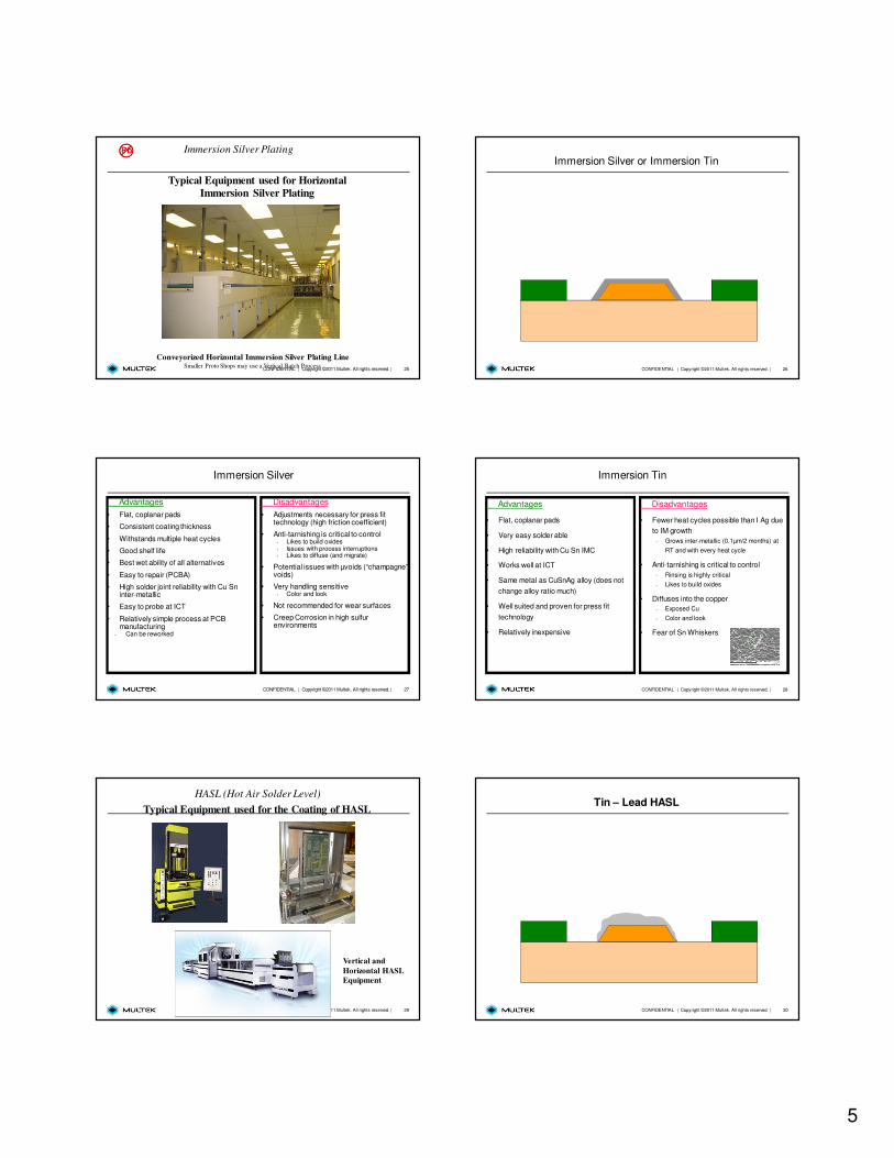
The main considerations in changing a HAL process from 63/37 Sn/Pb to SN100C
(Ni-stabilized Sn-0.7Cu) is:
38°C265°C(509)227°CSn-0.7Cu+Ni
67°C250°C(482)183°C63/37 Sn/Pb
PROCESS
WINDOW
PROCESS
TEMPERATURE
MELTING
POINT
ALLOY
�The higher melting point
*Source: Nihon Superior Co., LTD
Lead-Free Solder
40CONFIDENTIAL | Copyright ©2011 Multek. All rights reserved. |
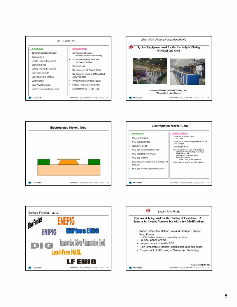
Corrosion of Copper Pad
After 6 Passes over Wave Soldering Machine 105°°°°C Preheat, 256°°°°C Solder Temperature, 4 seconds contact time
Original Pad
18µm Copper
Sn-37Pb Sn-3.0Ag-0.5Cu Sn-0.7Cu+NiSource: Florida CirTech, Inc.
LEAD-FREE HAL (Hot Air Level)
41CONFIDENTIAL | Copyright ©2011 Multek. All rights reserved. |
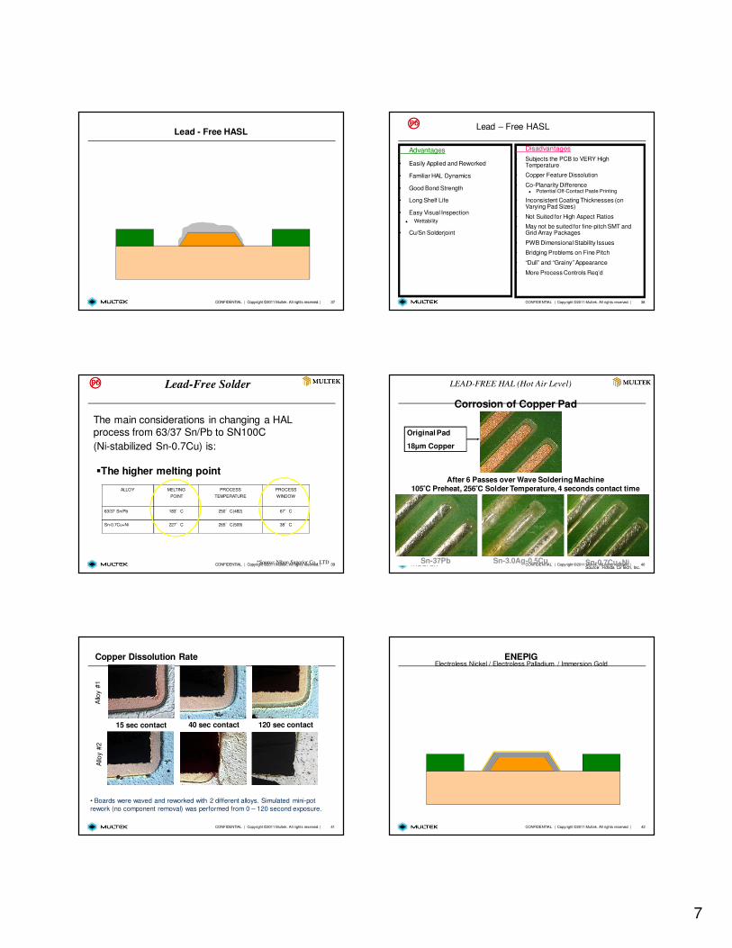
Copper Dissolution Rate
15 sec contact 120 sec contact40 sec contact
• Boards were waved and reworked with 2 different alloys. Simulated mini-pot
rework (no component removal) was performed from 0 – 120 second exposure.
Allo
y #
1A
lloy
#2
42CONFIDENTIAL | Copyright ©2011 Multek. All rights reserved. |
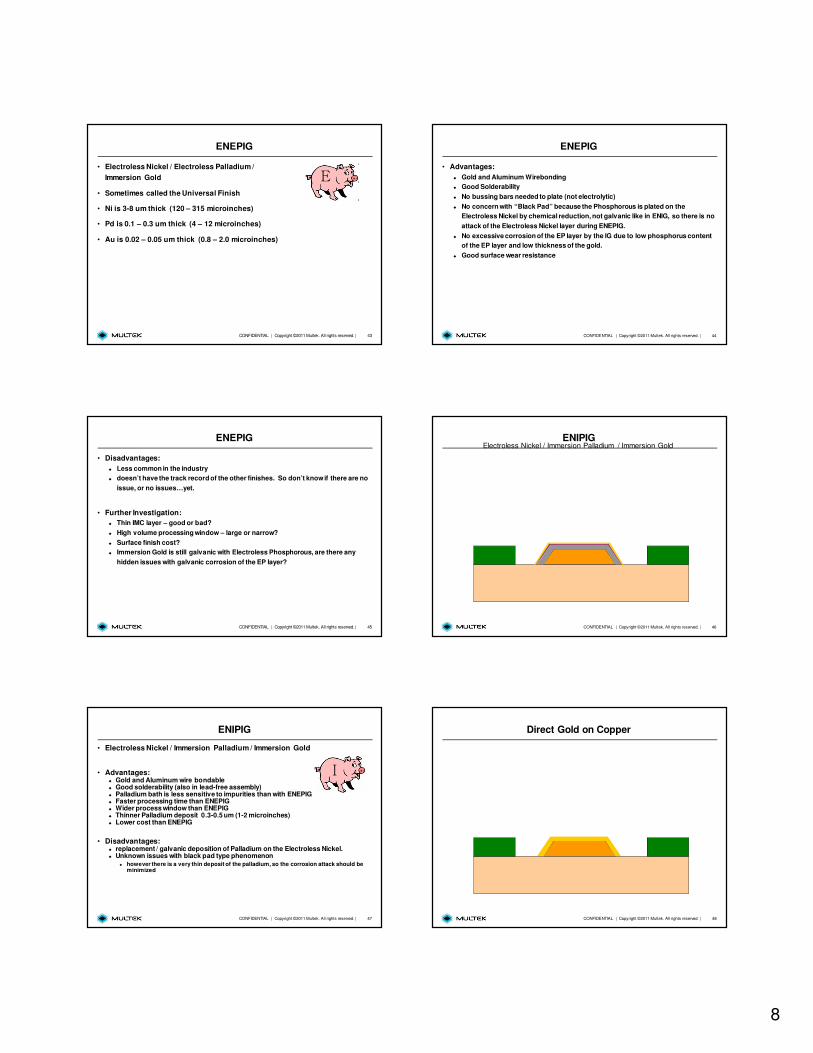
ENEPIGElectroless Nickel / Electroless Palladium / Immersion Gold
8
43CONFIDENTIAL | Copyright ©2011 Multek. All rights reserved. |
ENEPIG
• Electroless Nickel / Electroless Palladium /
Immersion Gold
• Sometimes called the Universal Finish
• Ni is 3-8 um thick (120 – 315 microinches)
• Pd is 0.1 – 0.3 um thick (4 – 12 microinches)
• Au is 0.02 – 0.05 um thick (0.8 – 2.0 microinches)
E
44CONFIDENTIAL | Copyright ©2011 Multek. All rights reserved. |
ENEPIG
• Advantages:
� Gold and Aluminum Wirebonding
� Good Solderability
� No bussing bars needed to plate (not electrolytic)
� No concern with “Black Pad” because the Phosphorous is plated on the
Electroless Nickel by chemical reduction, not galvanic like in ENIG, so there is no
attack of the Electroless Nickel layer during ENEPIG.
� No excessive corrosion of the EP layer by the IG due to low phosphorus content
of the EP layer and low thickness of the gold.
� Good surface wear resistance
45CONFIDENTIAL | Copyright ©2011 Multek. All rights reserved. |
ENEPIG
• Disadvantages:
� Less common in the industry
� doesn’t have the track record of the other finishes. So don’t know if there are no
issue, or no issues…yet.
• Further Investigation:
� Thin IMC layer – good or bad?
� High volume processing window – large or narrow?
� Surface finish cost?
� Immersion Gold is still galvanic with Electroless Phosphorous, are there any
hidden issues with galvanic corrosion of the EP layer?
46CONFIDENTIAL | Copyright ©2011 Multek. All rights reserved. |
ENIPIGElectroless Nickel / Immersion Palladium / Immersion Gold
47CONFIDENTIAL | Copyright ©2011 Multek. All rights reserved. |
ENIPIG
• Electroless Nickel / Immersion Palladium / Immersion Gold
• Advantages:� Gold and Aluminum wire bondable� Good solderability (also in lead-free assembly)� Palladium bath is less sensitive to impurities than with ENEPIG� Faster processing time than ENEPIG� Wider process window than ENEPIG� Thinner Palladium deposit 0.3-0.5 um (1-2 microinches)� Lower cost than ENEPIG
• Disadvantages:� replacement / galvanic deposition of Palladium on the Electroless Nickel.� Unknown issues with black pad type phenomenon
� however there is a very thin deposit of the palladium, so the corrosion attack should be minimized
I
48CONFIDENTIAL | Copyright ©2011 Multek. All rights reserved. |
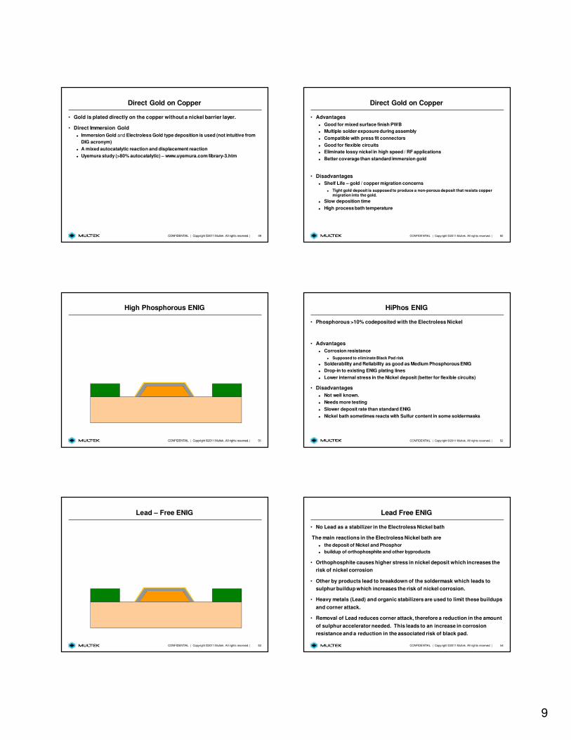
Direct Gold on Copper
9
49CONFIDENTIAL | Copyright ©2011 Multek. All rights reserved. |
Direct Gold on Copper
• Gold is plated directly on the copper without a nickel barrier layer.
• Direct Immersion Gold
� Immersion Gold and Electroless Gold type deposition is used (not intuitive from
DIG acronym)
� A mixed autocatalytic reaction and displacement reaction
� Uyemura study (>80% autocatalytic) – www.uyemura.com/library-3.htm
50CONFIDENTIAL | Copyright ©2011 Multek. All rights reserved. |
Direct Gold on Copper
• Advantages
� Good for mixed surface finish PWB
� Multiple solder exposure during assembly
� Compatible with press fit connectors
� Good for flexible circuits
� Eliminate lossy nickel in high speed / RF applications
� Better coverage than standard immersion gold
• Disadvantages
� Shelf Life – gold / copper migration concerns
� Tight gold deposit is supposed to produce a non-porous deposit that resists copper migration into the gold.
� Slow deposition time
� High process bath temperature
51CONFIDENTIAL | Copyright ©2011 Multek. All rights reserved. |
High Phosphorous ENIG
52CONFIDENTIAL | Copyright ©2011 Multek. All rights reserved. |
HiPhos ENIG
• Phosphorous >10% codeposited with the Electroless Nickel
• Advantages
� Corrosion resistance
� Supposed to eliminate Black Pad risk
� Solderability and Reliability as good as Medium Phosphorous ENIG
� Drop-in to existing ENIG plating lines
� Lower internal stress in the Nickel deposit (better for flexible circuits)
• Disadvantages
� Not well known.
� Needs more testing
� Slower deposit rate than standard ENIG
� Nickel bath sometimes reacts with Sulfur content in some soldermasks
53CONFIDENTIAL | Copyright ©2011 Multek. All rights reserved. |
Lead – Free ENIG
54CONFIDENTIAL | Copyright ©2011 Multek. All rights reserved. |
Lead Free ENIG
• No Lead as a stabilizer in the Electroless Nickel bath
The main reactions in the Electroless Nickel bath are
� the deposit of Nickel and Phosphor
� buildup of orthophosphite and other byproducts
• Orthophosphite causes higher stress in nickel deposit which increases the
risk of nickel corrosion
• Other by products lead to breakdown of the soldermask which leads to
sulphur buildup which increases the risk of nickel corrosion.
• Heavy metals (Lead) and organic stabilizers are used to limit these buildups
and corner attack.
• Removal of Lead reduces corner attack, therefore a reduction in the amount
of sulphur accelerator needed. This leads to an increase in corrosion
resistance and a reduction in the associated risk of black pad.
10
55CONFIDENTIAL | Copyright ©2011 Multek. All rights reserved. |
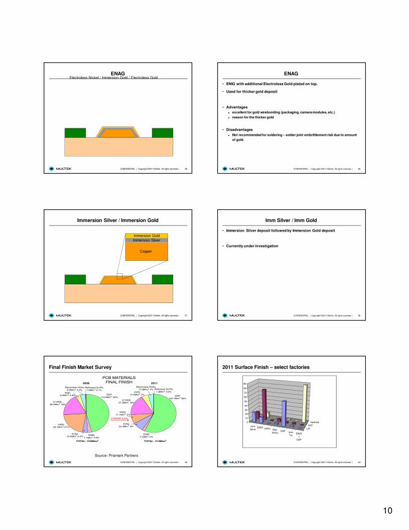
ENAGElectroless Nickel / Immersion Gold / Electroless Gold
56CONFIDENTIAL | Copyright ©2011 Multek. All rights reserved. |
ENAG
• ENIG with additional Electroless Gold plated on top.
• Used for thicker gold deposit
• Advantages
� excellent for gold wirebonding (packaging, camera modules, etc.)
� reason for the thicker gold
• Disadvantages
� Not recommended for soldering – solder joint embrittlement risk due to amount
of gold.
57CONFIDENTIAL | Copyright ©2011 Multek. All rights reserved. |
Immersion Silver / Immersion Gold
Immersion Gold
Immersion Silver
Copper
58CONFIDENTIAL | Copyright ©2011 Multek. All rights reserved. |
Imm Silver / Imm Gold
• Immersion Silver deposit followed by Immersion Gold deposit
• Currently under investigation
59CONFIDENTIAL | Copyright ©2011 Multek. All rights reserved. |
Final Finish Market Survey
PCB MATERIALSFINAL FINISH2006
TOTAL: 250Mm TOTAL: 319Mm
2011
OSP
183.7Mm 58%
OSP
115.0Mm 46%
HASL
52.1Mm 21%
HASL
17.1Mm 5%
Lf HASL
46.0Mm 18%
Lf HASL
57.3Mm 18%
ImSn9.0Mm 3.6%
ImSn
14.6Mm 5%
Electrolytic Ni/Au
8.5Mm 3.4%
Electrolytic Ni/Au
12.0Mm 4%Reflowed Sn/Pb
1.9Mm 0.7%Reflowed Sn/Pb
1.5Mm 0.0%
CAAGR 5.0%
ImAg
10.4Mm 4.2%2 ENIG
7.1Mm 2.8%2
2 2
2
2
2
2 2
2
2
2
2
2
2
2
ENIG
7.5Mm 2%2
ImAg
25.3Mm 8%2
Source: Prismark Partners
60CONFIDENTIAL | Copyright ©2011 Multek. All rights reserved. |
2011 Surface Finish – select factories
Imm
SilverENIG HASL Elec.
Ni/AuOSP
Imm
TinENIG
+
OSP
LFF
MFF
Handheld0
10
20
30
40
50
60
70
80
90
11
61CONFIDENTIAL | Copyright ©2011 Multek. All rights reserved. |
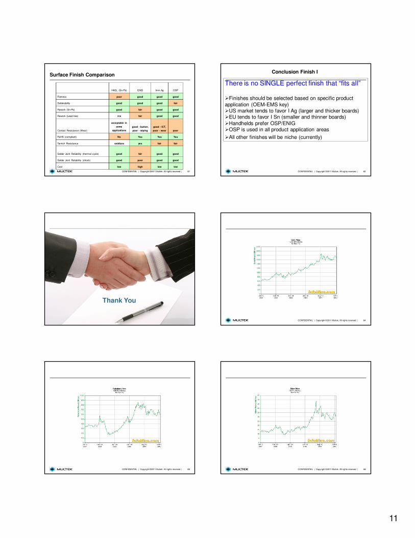
Surface Finish Comparison
HASL (Sn-Pb) ENIG Imm Ag OSP
Flatness poor good good good
Solderability good good good fair
Rework (Sn-Pb) good fair good good
Rework (Lead-free) n/a fair good good
Contact Resistance (Wear)
acceptable in
some
applications
good - button,
poor - wiping
good - ICT,
poor - wear poor
RoHS (compliant) No Yes Yes Yes
Tarnish Resistance oxidizes yes fair fair
Solder Joint Reliability (thermal cycle) good fair good good
Solder Joint Reliability (shock) good poor good good
Cost low high low low
62CONFIDENTIAL | Copyright ©2011 Multek. All rights reserved. |
Conclusion Finish I
There is no SINGLE perfect finish that “fits all”
�Finishes should be selected based on specific product
application (OEM-EMS key)�US market tends to favor I Ag (larger and thicker boards)�EU tends to favor I Sn (smaller and thinner boards)
�Handhelds prefer OSP/ENIG�OSP is used in all product application areas
�All other finishes will be niche (currently)
63CONFIDENTIAL | Copyright ©2011 Multek. All rights reserved. |
Thank You
Thank You
64CONFIDENTIAL | Copyright ©2011 Multek. All rights reserved. |
65CONFIDENTIAL | Copyright ©2011 Multek. All rights reserved. | 66CONFIDENTIAL | Copyright ©2011 Multek. All rights reserved. |
12
67CONFIDENTIAL | Copyright ©2011 Multek. All rights reserved. | 68CONFIDENTIAL | Copyright ©2011 Multek. All rights reserved. |
69CONFIDENTIAL | Copyright ©2011 Multek. All rights reserved. |