Embed Size (px)
Citation preview

NAVAL
POSTGRADUATE SCHOOL
MONTEREY, CALIFORNIA
THESIS
Approved for public release; distribution is unlimited
POWER LOSSES AND THERMAL MODELING OF A VOLTAGE SOURCE INVERTER
by
Michael Craig Oberdorf
March 2006
Thesis Advisor: Alexander Julian Second Reader: Robert Ashton

THIS PAGE INTENTIONALLY LEFT BLANK

i
REPORT DOCUMENTATION PAGE Form Approved OMB No. 0704-0188 Public reporting burden for this collection of information is estimated to average 1 hour per response, including the time for reviewing instruction, searching existing data sources, gathering and maintaining the data needed, and completing and reviewing the collection of information. Send comments regarding this burden estimate or any other aspect of this collection of information, including suggestions for reducing this burden, to Washington headquarters Services, Directorate for Information Operations and Reports, 1215 Jefferson Davis Highway, Suite 1204, Arlington, VA 22202-4302, and to the Office of Management and Budget, Paperwork Reduction Project (0704-0188) Washington DC 20503. 1. AGENCY USE ONLY (Leave blank)
2. REPORT DATE March 2006
3. REPORT TYPE AND DATES COVERED Master’s Thesis
4. TITLE AND SUBTITLE: Power Losses and Thermal Modeling of A Voltage Source Inverter
6. AUTHOR(S) Michael C. Oberdorf
5. FUNDING NUMBERS
7. PERFORMING ORGANIZATION NAME(S) AND ADDRESS(ES) Naval Postgraduate School Monterey, CA 93943-5000
8. PERFORMING ORGANIZATION REPORT NUMBER
9. SPONSORING /MONITORING AGENCY NAME(S) AND ADDRESS(ES) N/A
10. SPONSORING/MONITORING AGENCY REPORT NUMBER
11. SUPPLEMENTARY NOTES The views expressed in this thesis are those of the author and do not reflect the official policy or position of the Department of Defense or the U.S. Government. 12a. DISTRIBUTION / AVAILABILITY STATEMENT Approved for public release; distribution is unlimited
12b. DISTRIBUTION CODE
13. ABSTRACT (maximum 200 words) This thesis presents thermal and power loss models of a three phase IGBT voltage source inverter used in
the design of the 625KW fuel cell and reformer demonstration which is a top priority for the Office of Naval Research. The ability to generate thermal simulations of systems and to accurately predict a system’s response becomes essential in order to reduce the cost of design and production, increase reliability, quantify the accuracy of the estimated thermal impedance of an IGBT module, predict the maximum switching frequency without violating thermal limits, predict the time to shutdown on a loss of coolant casualty, and quantify the characteristics of the heat-sink needed to dissipate the heat under worst case conditions. In order to accomplish this, power loss and thermal models were created and simulated to represent a three phase IGBT voltage source inverter in the lab. The simulated power loss and thermal model data were compared against the experimental data of a three phase voltage source inverter set up in the Naval Postgraduate School power systems laboratory.
15. NUMBER OF PAGES
125
14. SUBJECT TERMS Power Losses Model, Thermal Modeling, IGBT, Voltage Source Inverter DC-AC
16. PRICE CODE
17. SECURITY CLASSIFICATION OF REPORT
Unclassified
18. SECURITY CLASSIFICATION OF THIS PAGE
Unclassified
19. SECURITY CLASSIFICATION OF ABSTRACT
Unclassified
20. LIMITATION OF ABSTRACT
UL
NSN 7540-01-280-5500 Standard Form 298 (Rev. 2-89) Prescribed by ANSI Std. 239-18

ii
THIS PAGE INTENTIONALLY LEFT BLANK
iii
Approved for public release; distribution is unlimited
POWER LOSSES AND THERMAL MODELING OF A VOLTAGE SOURCE INVERTER
Michael C. Oberdorf
Lieutenant, United States Navy B.S., Penn State University, 1999
Submitted in partial fulfillment of the requirements for the degree of
MASTER OF SCIENCE IN ELECTRICAL ENGINEERING
from the
NAVAL POSTGRADUATE SCHOOL March 2006
Author: Michael Craig Oberdorf
Approved by: Alexander Julian
Thesis Advisor
Robert Ashton Second Reader
Jeffery B. Knorr Chairman, Department of Electrical and Computer Engineering

iv
THIS PAGE INTENTIONALLY LEFT BLANK

v
ABSTRACT
This thesis presents thermal and power loss models of a three phase IGBT voltage
source inverter used in the design of the 625KW fuel cell and reformer demonstration
which is a top priority for the Office of Naval Research. The ability to generate thermal
simulations of systems and to accurately predict a system’s response becomes essential in
order to reduce the cost of design and production, increase reliability, quantify the
accuracy of the estimated thermal impedance of an IGBT module, predict the maximum
switching frequency without violating thermal limits, predict the time to shutdown on a
loss of coolant casualty, and quantify the characteristics of the heat-sink needed to
dissipate the heat under worst case conditions. In order to accomplish this, power loss
and thermal models were created and simulated to represent a three phase IGBT voltage
source inverter in the lab. The simulated power loss and thermal model data were
compared against the experimental data of a three phase voltage source inverter set up in
the Naval Postgraduate School power systems laboratory.

vi
THIS PAGE INTENTIONALLY LEFT BLANK

vii
TABLE OF CONTENTS
I. INTRODUCTION........................................................................................................1 A. OVERVIEW.....................................................................................................1 B. RESEARCH GOALS ......................................................................................6 C. APPROACH.....................................................................................................7
II. THERMAL MODEL...................................................................................................9 A. INTRODUCTION............................................................................................9 B. THERMAL MODEL GENERATION ........................................................10
1. Thermal System Defined ...................................................................10 2. Mathematical Model and Solution ...................................................11 3. Simulink Model ..................................................................................11
C. SUMMARY ....................................................................................................17
III. POWER LOSSES MODEL ......................................................................................19 A. REASON FOR DEVELOPMENT ...............................................................19 B. OVERVIEW...................................................................................................19 C. DEVELOPMENT OF POWER LOSSES MODEL ...................................20
1. Static Power Losses............................................................................20 a. Conduction Losses ..................................................................21 b. Blocking Losses.......................................................................29
2. Non-Static Power Losses ...................................................................29 a. Turn on/off Losses for the Upper IGBT ................................29 b. Turn on/off Losses for the Lower IGBT ................................30 c. Reverse Recovery Losses for the Lower Power Diode ...........32 d. Reverse Recovery Losses for the Upper Power Diode ...........33 e. Driving Power Losses..............................................................35
D. CREATING A THREE PHASE VSI POWER LOSSES MODEL...........35 E. SUMMARY ....................................................................................................37
IV. INITIAL SIMULATIONS ........................................................................................39 A. INTRODUCTION..........................................................................................39 B. POWER LOSSES SIMULATION ...............................................................39 C. THERMAL MODEL SIMULATION..........................................................42 D. SUMMARY ....................................................................................................47
V. EXPERIMENTAL DATA ACQUISTION..............................................................49 A. INTRODUCTION..........................................................................................49 B. CONSTRUCTION.........................................................................................49
1. Input Power ........................................................................................49 2. Three Phase Inductive Load .............................................................50 3. Measurement Devices ........................................................................51
C. DATA COLLECTION ..................................................................................53 1. First Data Run with No Coolant Flow Conducted on 08Jun05.....53

viii
2. Second Data Run with Coolant Flow Conducted on 07Jul05. .......74 D. SUMMARY ....................................................................................................83
VI. VALIDATION OF MODELS AND RESEARCH QUESTIONS ANSWERED ..............................................................................................................85 A. INTRODUCTION..........................................................................................85 B. VALIDATATION OF MODELS .................................................................85
1. Power Losses Simulation vs. Total Experimental Input Power ....85 2. Thermal Model Simulation Junction Temperatures vs.
Experimental IGBT Junction Temperature....................................87 C. SIMULATION TO ANSWER RESEARCH QUESTION.........................87
1. Simulation to Determine IGBT Junction Temperature at Different Frequencies at Maximum Design Conditions for the 625KW Fuel Cell Reformer Project for ONR.................................87
D. RESEARCH QUESTIONS READDRESSED ............................................90
VII. CONCLUSIONS ........................................................................................................93 A. CHAPTER OVERVIEW ..............................................................................93 B. SUMMARY ....................................................................................................93 C. CONCLUSIONS ............................................................................................94 D. FUTURE WORK...........................................................................................94
APPENDIX A.........................................................................................................................97
APPENDIX B .......................................................................................................................101 A. MATLAB M-FILE FOR POWER LOSSES MODEL.............................101
LIST OF REFERENCES....................................................................................................103
INITIAL DISTRIBUTION LIST .......................................................................................105
ix
LIST OF FIGURES
Figure 1. Overview of Thesis Model........................................................................... xviii Figure 2. Historic Shipboard Electrical Generator Capacities [From 3]...........................2 Figure 3. Comparison of IPS vs. Conventional Power Plants[From 5] ............................4 Figure 4. Power Electronics Building Blocks [From 5]....................................................5 Figure 5. Semikron Thermal Model of System showing 9th Order System Reduced
to three 4th Order Systems [From 6] ................................................................12 Figure 6. Thermal Model of a Fourth Order System [After 6]........................................13 Figure 7. Semikrons Simplified Thermal Model for IGBT and Free Wheeling Diode
[From 6] ...........................................................................................................14 Figure 8. Simulink Model of 4th Order Transfer Function Representing the Thermal
model of the IGBT junction to Module Case system ......................................14 Figure 9. Simulink Model of 4th Order Transfer Function Representing the Thermal
model of the Diode junction to Module Case system......................................15 Figure 10. Simulink Model of 1st Order Transfer Function Representing the Thermal
model of the Heatsink to Ambient Temperature.............................................16 Figure 11. Total Thermal Model of Inverter Module which includes the IGBT and
Diode junction temperatures ............................................................................17 Figure 12. Overview and Breakdown of Total Power Losses[From 6] ............................20 Figure 13. SKiiP 942GB120-317CTV Module Topology showing user defined
positive current direction [From Ref 6] ...........................................................21 Figure 14. Simulink Model of Upper IGBT Conduction Losses ......................................22 Figure 15. SKiiP Module Topology showing Lower Power Diode Conduction
conditions [From 6]..........................................................................................23 Figure 16. Simulink Model of Lower Power Diode Conduction Losses ..........................24 Figure 17. Electrical Model of SKiiP Module Topology showing user defined
negative current direction [From 6]. ................................................................25 Figure 18. Simulink Model of Lower IGBT Conduction Losses......................................26 Figure 19. SKiiP Module Topology showing Upper Power Diode Conduction
conditions [From 6]..........................................................................................27 Figure 20. Simulink Model of Upper Power Diode Conduction Losses...........................28 Figure 21. Simulink Model of Upper IGBT Turn On/Off Power Losses .........................30 Figure 22. Simulink Model of Lower IGBT Turn On/Off Power Losses.........................31 Figure 23. Simulink Model of Lower Power Diode Reverse Recovery Power Losses ...33 Figure 24. Simulink Model of Upper Power Diode Reverse Recovery Power Losses....35 Figure 25. Simulink Model of Summation of Power Losses for one SKiiP
942GB120-317CTV VSI ................................................................................36 Figure 26. Simulink Model of Summation of Power Losses for Three SKiiP
942GB120-317CTV VSI ................................................................................37 Figure 27. Simulink Simulation of Power Losses for Semikron Three Phase VSI..........40 Figure 28. Simulink Simulation Showing 65.6 Watts of Power Losses for Lower
IGBT ................................................................................................................41
x
Figure 29. Simulink Simulation of 35.5 Watts of Power Losses for Upper Power Diode................................................................................................................41
Figure 30. Thermal Resistance of NWK 40 Water Cooled Heatsink. [From 6] ...............43 Figure 31. Simulink Simulated Temperature at Inverter Case/Heatsink Boundary
from Thermal Model Using Power Losses Generated from Power Losses Simulation ........................................................................................................44
Figure 32. Simulink Simulated IGBT Junction Temperature from Thermal Model Using Power Losses Generated from Power Losses Simulation .....................45
Figure 33. Simulink Simulated Diode Junction Temperature from Thermal Model Using Power Losses Generated from Power Losses Simulation .....................46
Figure 34. Basic Block Diagram of Lab Equipment Setup for Experimental Data Collection.........................................................................................................50
Figure 35. Semikron DC-AC VSI Module used for the 625KW Fuel Cell and Reformer Demonstration Set Up to Match Simulink Models .........................51
Figure 36. STATCO ENERGY PRODUCTS CO. 12.1kVA VARIAC ...........................52 Figure 37. Y Connected MTE RL-10002 0.30mH Inductor .............................................52 Figure 38. Load Voltage 568mVpp using a High Voltage Differential Probe on Scale
1/500: Therefore showing 100Vrms (Equation 15). ..........................................54 Figure 39. Load Current for Data Run #1 of 56.2mVpp using two current probes and
the summing function with 50A/div at the 10mV scale (Equation 16). ..........55 Figure 40. Matlab Plot of Rise in Thermal Resistor Temperature with no coolant flow
and input power of 642 Watts for Semikron Source Inverter SKiiP942GB120-317CTV with an ambient temperature of 24°C...................70
Figure 41. Thermal Model Approximation of 1st Order System [6]. ................................70 Figure 42. CFTOOL fitting of Thermal Data to extract tau= R x C. ................................71 Figure 43. Predicted Theoretical Tj based on Input of Pmax with a Loss of Coolant
Casualty............................................................................................................74 Figure 44. Load Voltage 564mVpp using a High Voltage Differential Probe on Scale
1/500: Therefore showing 100Vrms (Equation 18). ..........................................75 Figure 45. Load Current for Data Run #2of 56.0mVpp using two current probes and
the summing function with 50A/div at the 10mV scale (Equation 19). ..........76 Figure 46. Matlab Plot of Rise in Thermal Resistor Temperature with coolant flow
and input power of 578 Watts for Semikron Source Inverter SKiiP942GB120-317CTV with an ambient temperature of 25.4°C................82
Figure 47. Simulated IGBT Junction Temperature from Simulink Thermal Model Using Maximum Design Parameters for the 625Kw Fuel Cell Reformer Project at a PWM switching frequency of 5kHz. ............................................88
Figure 48. Simulated IGBT Junction Temperature from Simulink Thermal Model Using Maximum Design Parameters for the 625Kw Fuel Cell Reformer Project at a PWM Switching frequency of 7 kHz............................................89
Figure 49. Simulated IGBT Junction Temperature from Simulink Thermal Model Using Maximum Design Parameters for the 625Kw Fuel Cell Reformer Project at a PWM switching frequency of 7 kHz. ...........................................89
xi
LIST OF TABLES
Table 1. List of initial Variables for Thermal Model.....................................................42 Table 2. Summary of Simulated Temperatures of a Semikron Skip Semikron three
phase VSI using PWM at a switching frequency of 5 kHz with an input voltage of 100Vdc, output current of 100A, and an output voltage of 100 VAC at 60Hz with an ambient temperature of 25.5°C. ...................................46
Table 3. Data Run#1 Conducted on 08Jun05 Recorded Data for Voltage Source Inverter with no water supplied to heat sink....................................................69
Table 4. Equations Relating First Order Solution of the Thermal System to the Electrical Equivalent Circuit[7] .......................................................................71
Table 5. Matlab CFTOOL Output for solving 1st Order Equivalent of Thermal System..............................................................................................................72
Table 6. Calculations and Assumptions for Determining the constant A in Buildup Equation in Table 5..........................................................................................73
Table 7. Equations and Matlab Code to Determine Time to Shutdown with a Loss of Coolant Casualty..........................................................................................73
Table 8. Data Run #2 Completed on 07Jul05.Recorded Data for Voltage Source Inverter with water supplied to heat sink at a rate of 5.31 l/min with water at a temperature of 21.5°C. ..............................................................................81
Table 9. Summary of Collected and Extracted Data from Data Run #1........................83 Table 10. Summary of Collected and Extracted Data from Data Run #2........................83 Table 11. Summary of Simulated IGBT Power Losses. ..................................................85 Table 12. Summary of Simulated Power Diode Power Losses. ......................................86 Table 13. Summary of Simulated Power Losses for One Three Phase Inverter..............86 Table 14. Summary of Experimental Input Power ..........................................................86 Table 15. Comparison of Experimental and Simulated Power Losses Data with
Percent Error ....................................................................................................86 Table 16. Comparison of Simulated vs. Experimental Thermal Response with
Percent Error ....................................................................................................87 Table 17. Summary of Simulated IGBT Junction Temperature for 625 Fuel Cell
Reformer Demonstration for different Frequencies based on Maximum Design Parameters and Maximum Ambient Temperature...............................90
Table 18. Summary of Thesis Results and Goals ............................................................94

xii
THIS PAGE INTENTIONALLY LEFT BLANK

xiii
ACKNOWLEDGMENTS
First, I would like to thank my advisor, Professor Alex Julian for his guidance in
this thesis research. He always had suggestions and new ideas when I ran into problems
with the modeling of the system, and his help in understanding the hardware was
invaluable. I would like to thank my Co-Advisor Professor Ashton for all the help he
gave me on my introduction and background information. I would like to thank Tom
Fikse from, Naval Surface Warfare Center for the funding and equipment which allowed
me to complete my thesis. Several of my fellow students also deserve to be recognized.
Carl Trask and Greg Moselle were always willing to help out with brainstorming,
troubleshooting, and coding. I would like to thank my parents for the love and support
they have given me. Finally, I would like to thank my wife for her support through all
the years we have been married, I am the man I am today because of her.

xiv
THIS PAGE INTENTIONALLY LEFT BLANK

xv
LIST OF ABBREVIATIONS, ACRONYMS, AND SYMBOLS
VSI Voltage Source Inverter
ONR Office of Naval Research
FPGA Field Programmable Gate Array
NPS Naval Postgraduate School
LOCC Loss of Coolant Casualty
IPS Integrated Power System
COTS Commercial Off The Shelf Technology
PEBB Power Electronics Building Block
AC Alternating Current
DC Direct Current
EMALS Electromagnetic Aircraft Launching System
IGBT Insulated Gate Bipolar Transistor
OOD Officer Of the Deck
FEL Free Electron Laser
NWSC Naval Warfare Service Center
TMS Thermal Management System
EM Electro Magnetic

xvi
THIS PAGE INTENTIONALLY LEFT BLANK
xvii
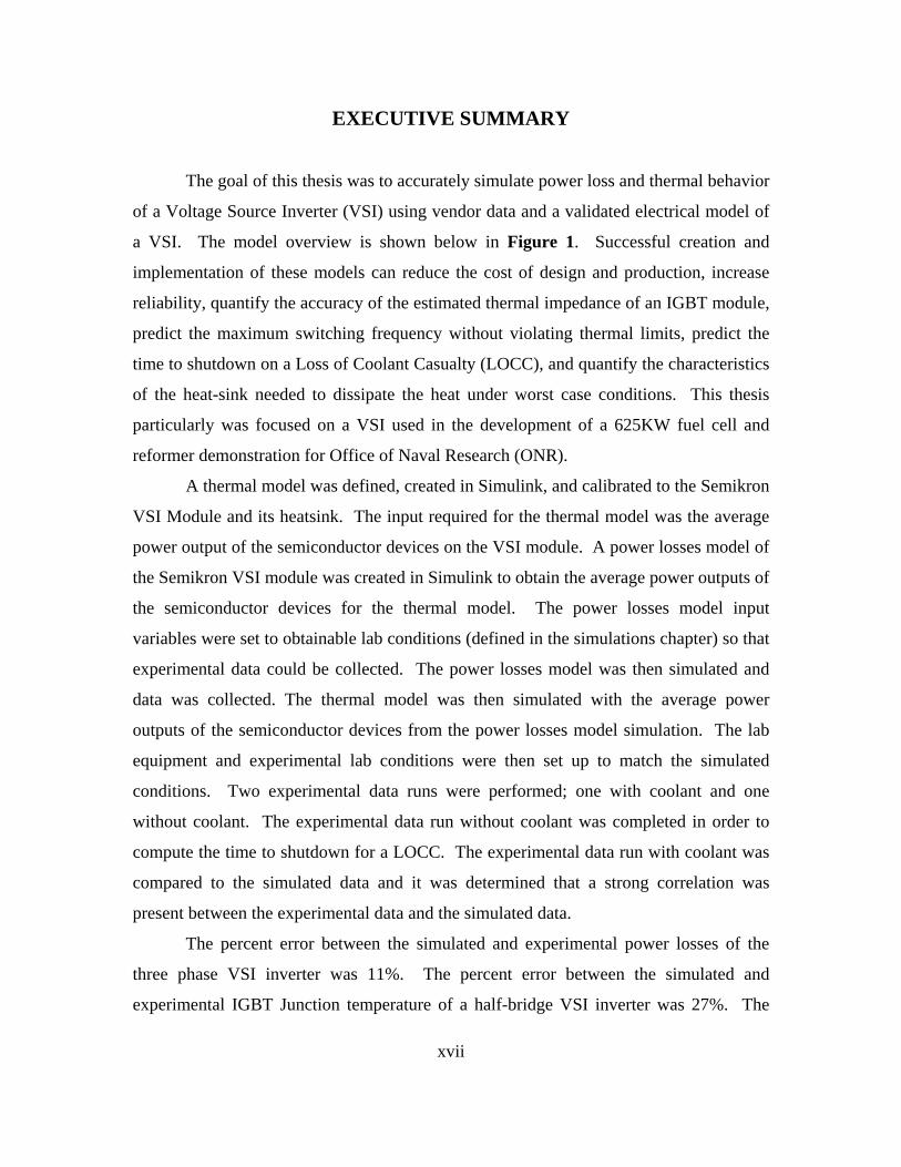
EXECUTIVE SUMMARY The goal of this thesis was to accurately simulate power loss and thermal behavior
of a Voltage Source Inverter (VSI) using vendor data and a validated electrical model of
a VSI. The model overview is shown below in Figure 1. Successful creation and
implementation of these models can reduce the cost of design and production, increase
reliability, quantify the accuracy of the estimated thermal impedance of an IGBT module,
predict the maximum switching frequency without violating thermal limits, predict the
time to shutdown on a Loss of Coolant Casualty (LOCC), and quantify the characteristics
of the heat-sink needed to dissipate the heat under worst case conditions. This thesis
particularly was focused on a VSI used in the development of a 625KW fuel cell and
reformer demonstration for Office of Naval Research (ONR).
A thermal model was defined, created in Simulink, and calibrated to the Semikron
VSI Module and its heatsink. The input required for the thermal model was the average
power output of the semiconductor devices on the VSI module. A power losses model of
the Semikron VSI module was created in Simulink to obtain the average power outputs of
the semiconductor devices for the thermal model. The power losses model input
variables were set to obtainable lab conditions (defined in the simulations chapter) so that
experimental data could be collected. The power losses model was then simulated and
data was collected. The thermal model was then simulated with the average power
outputs of the semiconductor devices from the power losses model simulation. The lab
equipment and experimental lab conditions were then set up to match the simulated
conditions. Two experimental data runs were performed; one with coolant and one
without coolant. The experimental data run without coolant was completed in order to
compute the time to shutdown for a LOCC. The experimental data run with coolant was
compared to the simulated data and it was determined that a strong correlation was
present between the experimental data and the simulated data.
The percent error between the simulated and experimental power losses of the
three phase VSI inverter was 11%. The percent error between the simulated and
experimental IGBT Junction temperature of a half-bridge VSI inverter was 27%. The
xviii
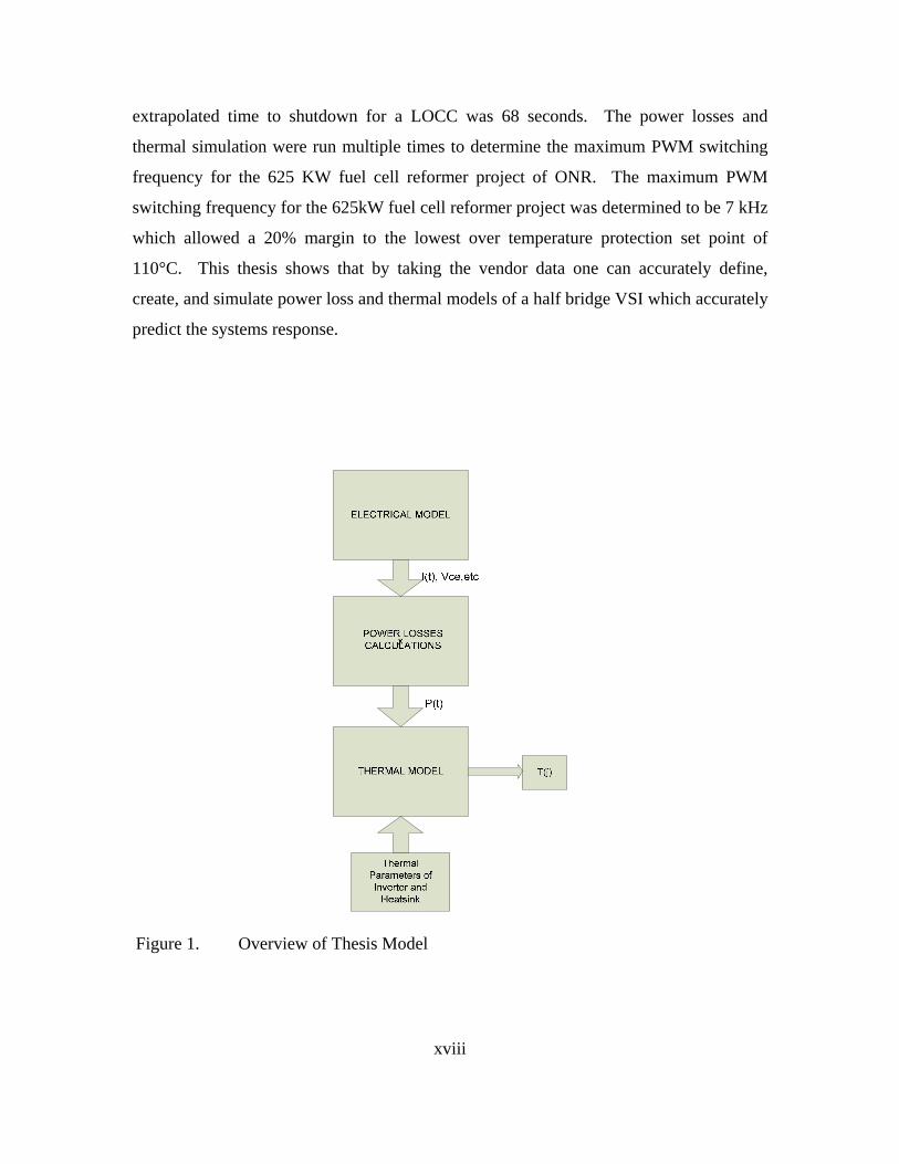
extrapolated time to shutdown for a LOCC was 68 seconds. The power losses and
thermal simulation were run multiple times to determine the maximum PWM switching
frequency for the 625 KW fuel cell reformer project of ONR. The maximum PWM
switching frequency for the 625kW fuel cell reformer project was determined to be 7 kHz
which allowed a 20% margin to the lowest over temperature protection set point of
110°C. This thesis shows that by taking the vendor data one can accurately define,
create, and simulate power loss and thermal models of a half bridge VSI which accurately
predict the systems response.
Figure 1. Overview of Thesis Model

1
I. INTRODUCTION
A. OVERVIEW As the U. S. Navy moves toward a smaller more sophisticated fleet whose ships
require less military personnel to operate them and becomes more dependent on
electronics, the need to quantify the heat dissipated by electronic loads becomes
paramount. As the number of electronic devices and inefficient weapon systems increase
the ability to accurately quantify and predict the heat loads will allow ships to move from
concentrated heat loads (i.e. propulsion system) to distributed heat loads (i.e. multiple
electronic converters).
Today, one of the acronyms of interest is COTS (Commercial Off The Shelf)
technology. The secretary of the Navy stated in January 2000 that electric drive would be
used to propel all future Navy warships.
“Changes in propulsion systems fundamentally change the character and the
power of our forces. This has been shown by the movement from sails to steam or from
propeller to jet engines… More importantly, electric drive, like other propulsion
changes, will open immense opportunities for redesigning ship architecture, reducing
manpower, improving ship life, reducing vulnerability and allocating a great deal more
power to war-fighting applications” [From 1].
The Navy’s DD(X) ship program will be constructed with an Integrated Power
System (IPS) to utilize all available shipboard power more efficiently and to unlock
propulsion power for high-powered advanced electric launch, weapons, and sensor
systems [3].
The Navy has had many transitions in its lineage that have changed the way we
fight wars and build ships. The battleship was considered a measure of a country’s naval
strength during World War I and World War II. But in World War II, the aircraft carrier
proved to be superior to the battleship during the Battle of Midway and the age of the
carrier began. The submarine also proved to be a stealthy and effective weapon during
World War II. The submarine from its beginning days of the Turtle to the newest
Virginia Class nuclear submarine, has truly redefined the battle space. Although there

2
have been many inventions and changes within the Navy the standard power distribution
architecture has remained the same for the last hundred years although electrical power
demand has increased (Figure 2), [2].
INCREASING SHIPBOARD POWER DEMAND
Figure 2. Historic Shipboard Electrical Generator Capacities [From 3]
So, why is the amount of power demand increasing and what does that have to do
with power loss and thermal modeling of a Voltage Source Inverter (VSI)? The amount
of increased power demand stems from the introduction of new technology such as the
Electro-Magnetic Aircraft Launching System (EMALS), Electro-Magnetic (EM) rail-
gun, Free Electron Laser (FEL), and high power radar. One technical report from the
Naval Surface Warfare Center (NSWC) dated July 2003 concluded that the new
generation ship will not be able to incorporate all these above listed thermal loads without
a more modernized cooling system [4]. Further, compounding the thermal load is the
introduction of distributed heat sources in the form of electronic converters. The
objective of the thermal survey was to identify, quantify and document heat loads
generated by naval systems in order to project cooling requirements for the future [4].

3
The following quotation is the summary of this study:
“The implementation of the design features of new electric distributed loads to
achieve these objectives for the next generation of warships results in the generation of
additional waste heat. Thermal issues are key in electronic product development at all
levels of the electronic product hierarchy, from components such as the chip to the
transfer of heat throughout ship systems and out to sea. Shrinking component sizes are
resulting in increasing the volumetric heat generation rates and surface heat fluxes in
many devices. The rate of heat flux is expected to eventually top 1000W/cm2 due to
material advances, smaller electronics components and faster switching speeds. The
addition of advanced power electronics, advanced radar, dynamic armor, and weapons
systems such as the EM railgun and the Free Electron Laser in future Naval Combatants,
will result in heat loads eventually requiring a significant increase in cooling capacity”
[From 4].
As the Navy moves towards IPS and away from conventional propulsion it
introduces more heat generation from power electronic loads that will need to be
quantified in order to accurately design cooling systems for future ships. The power
requirements for the new high power weapons such as the EM railgun and the FEL are so
demanding on the cooling system a Thermal Management System (TMS) for the entire
ship might need to be designed [4]. The TMS would contain thermal models of all
dissipatory equipment and its heat load given its current readiness condition. For
instance, once an Officer Of the Deck (OOD) gives the command to fire the EM railgun,
the TMS may override the command until there is sufficient cooling capacity. The ability
to provide a robust cooling system capable of handling all heat loads becomes a difficult
problem when one tries to minimize the size, weight and cost of the ship. The thermal
loads of COTS equipment may also necessitate the inclusion of a TMS; COTS equipment
generally dumps heat directly into the occupied area. This distributed thermal loading
may quickly overwhelm Heating Ventilation and Air Conditioning (HVAC) systems.
Further, new modern reduced sized electronics may require special attention, because the
power density and thus heat generation have been increased. The ships cooling capacity

4
might need to be modified in order to handle these newly introduced loads. IPS versus
conventional propulsion is shown in Figure 3 [5].
Figure 3. Comparison of IPS vs. Conventional Power Plants[From 5]
So why is the navy going to IPS? IPS has less prime mover machinery which
equates to less infrared and acoustic signatures. IPS requires a smaller machinery room
and propulsion plant which will reduce the fuel consumption over the life of the ship by
an anticipated 15-20%. The reduction in weight will equate to reduced ships
displacement and a faster ship. IPS is a modular design which will reduce construction,
repair, and modernization costs. IPS technology has longer Mean Time Between Failures
(MBTF) of propulsion components. The above characteristics equates to reduced
manpower for operations up to 50% and reduced life cycle costs up to 50%. IPS
propulsion motors have shorter electrical drive shafts when compared to the legacy
systems, allowing an increase in the ships compartmentalization and survivability. Most
importantly, the mechanical power only available for propulsion is unleashed for other

5
high power loads that could not possibly be energized by the ships service bus. The
overall design of the IPS system doesn’t require the extensive hydraulic and pneumatic
systems, but instead utilizes electro-mechanical systems which reduce both overall cost
and weight. It provides a more robust electrical power system capable of handling the
next generation weapons such as the EM railgun and the FEL [5].
The ships zonal power distribution architecture utilizes both converters and
inverters. The inverters and converters of the future could be made of Power Electronic
Building Blocks (PEBB) technology. The PEBB will be able to convert ac to dc, buck
and/or boost dc to dc, convert ac from one frequency to another, and invert dc back to ac.
Since PEBB are pre-tested “plug and play” models, any system assembled with PEBB is
pre-engineered and pre-tested to a certain extent. architecture. PEBB philosophy dictates
that large converters will be constructed by series and/or parallel combinations of
common blocks; Voltage can be increased by series connected PEBB while current can
be increased by parallel connected PEBB (Figure 4) [4, 5].
Figure 4. Power Electronics Building Blocks [From 5]
The concept PEBB contains a microprocessor/FPGA controller that allows the
module to be programmed for a variety of different functions as listed in the previous
paragraph. Ultimately, the PEBB constructed will be able to self-protect and limit stress
to other common bus connected electronic equipment. The PEBB itself is made up of
IGBT (or other electronic switching devices), diodes, laminate buses, isolated gate
drivers, controller interface card, electrolytic capacitors, etc. The switching devices and
diodes dissipate the majority of the heat as they conduct and switch from one state to

6
another. The thermal properties of the PEBB must be understood and tabulated in order
to properly integrate a useable converter into a military environment. Thus, this thesis
addresses the thermal characterization of a 625KW fuel cell converter constructed from
COTS PEBB. The ability to account for the heat generated so that it may be dissipated is
why the PEBB and IPS are relevant to this thesis.
Further, as industry constantly decreases the size of electronics the efficiency
doesn’t increase at the same rate which causes increased thermal stresses. The ability to
characterize the thermal constraints of components based on the given controller
architecture, layout, and environment becomes essential in order to reduce costs of design
and production.
B. RESEARCH GOALS During the development of a controller for a 625KW fuel cell inverter, it became
necessary to determine the maximum switching frequency of the semiconductors in the
PEBB without violating thermal limits. A high switching frequency is generally desired
to reduce the size of the filtering components. However, thermal losses increase as
frequency increases. This necessitated a study of the power losses and thermal
characteristics of the VSI. The following are the thesis goals for the power loss and
thermal modeling of a VSI :
• Model the power losses for a three phase VSI system using Simulink.
• Model the thermal behavior of a VSI system using Simulink.
• Compare the simulations to experimental measurements in order to validate
models.
• Quantify the accuracy of the estimated thermal impedance of an IGBT module.
• Predict the maximum switching frequency without violating thermal limits.
• Predict the time to shutdown on a Loss of Coolant Casualty (LOCC).
• Quantify the characteristics of the heat-sink needed to dissipate the heat under
worst case conditions.
The Comparison of the simulated data and the experimental data will be used to
validate the computer modeling of the system.

7
C. APPROACH The thermal model was defined and then created in Simulink given a valid
electrical model. The thermal model was calibrated to the Semikron VSI module (i.e.
PEBB) and its heatsink [6]. The input required in the thermal model was the average
power output of the semiconductor devices on the VSI module. In order to simulate the
average power output of the semiconductor devices, a power loss model of the Semikron
VSI module was created in Simulink. The power loss model input variables were set to
obtainable lab conditions. The model was then simulated and data was collected for
verification with experimental results. The thermal model was then simulated with the
average power outputs of the semiconductor devices from the power loss model
simulation. The lab equipment and experimental lab conditions were then set up to
match the simulated conditions. Two experimental data runs were performed: one with
coolant and one without coolant. The experiment without coolant was completed in order
to compute shutdown time for an LOCC. The experiment with coolant was compared to
the simulated data to determine if a correlation was present. Models were validated
based on the results.
D. THESIS ORGANIZATION
Chapter I is an overview of the research effort and the layout of the thesis.
Chapter II is a presents the thermal model of the IGBT half bridge dc-ac voltage
source inverter.
Chapter III presents the power losses model which computes the amount of power
losses inside the voltage source inverter along with the load in order to verify the
thermal model.
Chapter IV presents the power losses and thermal model simulation results.

8
Chapter V Experimental Data Acquisition: experimental results from the lab built
prototype in order to verify thermal model.
Chapter VI Validation of Models by comparisons between the simulated and
experimental data and readdressing the research questions.
Chapter VII provides conclusions and future research opportunities.
The appendices provide Matlab computer code, data sheets, and application notes
for the models constructed in this thesis.

9
II. THERMAL MODEL
A. INTRODUCTION In order to accomplish the research goals of this thesis a thermal model of a
voltage source inverter (VSI) was created. Specifically, it was created for a Semikron
SKiiP 942GB120-317CTV VSI. The Semikron SKiiP package was chosen because it
was the VSI that was used in the design of ONR’s 625KW fuel cell and reformer
demonstration. It was also used because it had a thermal resistor in close proximity to the
IGBT junction. The thermal resistor allowed experimental temperature to be collected
which could be compared to the simulated thermal model data of the IGBT junction
temperature. Without this feature a contact pyrometer or other thermal device would
have to be installed in order to measure the actual IGBT junction temperature.
The thermal model of the system was characterized by using the vendor
application notes and data sheets. Once the thermal model was defined, a mathematical
model representation of the system was created and solved. The mathematical model was
then implemented in a Simulink Model. The Simulink Model was then calibrated to the
data sheets for the Semikron SKiiP 942GB120-317CTV by creating a Matlab M-File for
the initial variables of the thermal model. The input required for the thermal model was
average power of the semiconductor devices on the Semikron module. Therefore, in
order to determine the thermal response of the system a power losses model was created
which is discussed in Chapter III.
The following are the benefits of creating a valid thermal model which predicts
the temperature of the IGBT and diode junctions in a voltage source inverter:
o To reduce the cost of design and production.
o Increase reliability.
o Quantify the accuracy of the estimated thermal impedance of an IGBT
module.
o Predict the maximum switching frequency without violating thermal
limits.

10
o Predict the time to shutdown on a Loss of Coolant Casualty (LOCC).
o To quantify the characteristics of the heat-sink needed to dissipate the heat
under worst case conditions.
B. THERMAL MODEL GENERATION
1. Thermal System Defined The first step in thermal modeling of a VSI was to characterize the system.
Although a more detailed system model is a ninth order system represented in Figure 5.
The vendor has stated and showed that the thermal response of the IGBT and diode
junction-case temperatures can be approximated by the solution of a fourth order system.
The data necessary to represent the fourth order approximation of the system is provided
in the vendor’s data sheet located in Appendix A. Each fourth order system from a
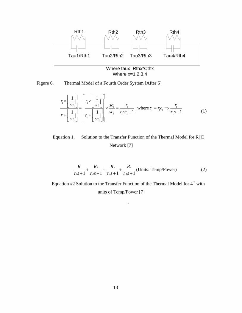
thermal stand point can be characterized as a fourth order R||C Load as seen in Figure 6
[6].
The model of the system is based on the vendor’s representation of a fourth
ordered system. As seen in Figure 7, the topology of the thermal model is made up of
half of a half bridge inverter which includes one IGBT and one free wheeling diode. The
vendors thermal model in the application notes makes some notable assumptions. First,
the temperature drop from the case of the IGBT module to the heat sink is neglected.
Second, the thermal coupling between the IGBT and the free wheeling diode is neglected.
Instead of coupling, the application notes inform the user to use the hottest modeled
semiconductor device junction temperature to be the junction temperature of both
devices. This assumption is made due to the semiconductor devices close proximity to
each other. The validity of these assumptions will be discussed in the conclusions
chapter [6].
In order to determine the temperature of the IGBT junction temperature (Tj/T1)
(Figure 7), a model of three systems must be created. One of the systems is a fourth
order system, which is the model of thermal resistance and capacitance(RthC) from IGBT
junction to case, which represents the temperature drop from the IGBT junction to case of
11
the SKiiP package. The next thermal boundary is the RthC from the case of the SKiiP
package to attached heatsink. These thermal constants are due to the thermal paste
applied and the amount of surface area for heat to dissipate. The vendor has determined
that difference in temperature between the case of the IGBT module and the heat sink is
negligible compared to the other thermal transfer functions and this system also
neglected. The last system represents the RthC model is from the water-cooled heatsink
to ambient temperature and is represented by a first ordered model.
In order to determine the temperature at the junction of the free wheeling diode
another 4th order system was created as seen in Figure 7. The system was that of a diode
junction to inverter module case. Again, the thermal boundary from the case of the SKiiP
package to attached heatsink is neglected. The last system represents the RthC model is
from the water-cooled heatsink to ambient temperature and is represented by a first
ordered model.
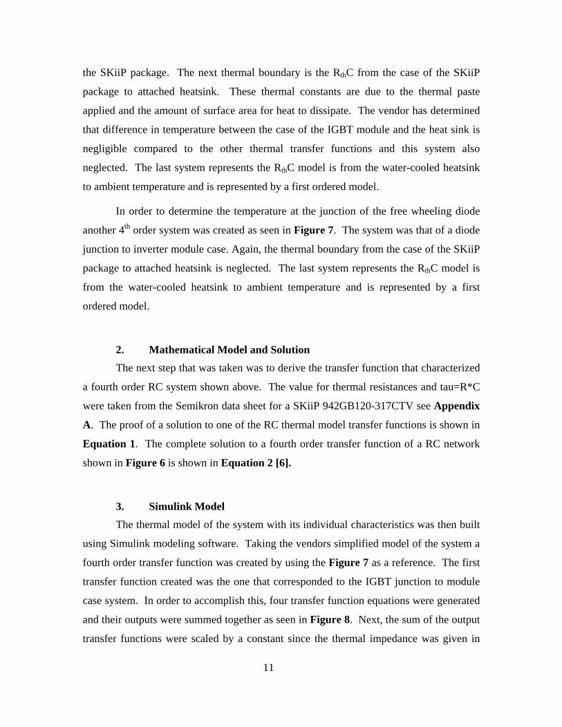
2. Mathematical Model and Solution The next step that was taken was to derive the transfer function that characterized
a fourth order RC system shown above. The value for thermal resistances and tau=R*C
were taken from the Semikron data sheet for a SKiiP 942GB120-317CTV see Appendix
A. The proof of a solution to one of the RC thermal model transfer functions is shown in
Equation 1. The complete solution to a fourth order transfer function of a RC network
shown in Figure 6 is shown in Equation 2 [6].
3. Simulink Model The thermal model of the system with its individual characteristics was then built
using Simulink modeling software. Taking the vendors simplified model of the system a
fourth order transfer function was created by using the Figure 7 as a reference. The first
transfer function created was the one that corresponded to the IGBT junction to module
case system. In order to accomplish this, four transfer function equations were generated
and their outputs were summed together as seen in Figure 8. Next, the sum of the output
transfer functions were scaled by a constant since the thermal impedance was given in

12
milli-Kelvin/Watt in the vendor datasheet (see Appendix A). The output of the sum of
the transfer functions in Figure 8 represents a change in temperature.
Figure 5. Semikron Thermal Model of System showing 9th Order System Reduced to three 4th Order Systems [From 6]
13
Rth1
Tau1/Rth1
Rth3 Rth4
Tau2/Rth2 Tau3/Rth3 Tau4/Rth4
Rth2
Where taux=Rthx*CthxWhere x=1,2,3,4
Figure 6. Thermal Model of a Fourth Order System [After 6]
1 11 1 1 1 1
1 1 11 1 1 1
11 1
1 1
, where1 11 1
r rsc sc sc r rrc
sc r sc sr r
sc sc
ττ
⎡ ⎤⎡ ⎤ ⎡ ⎤× ×⎢ ⎥⎢ ⎥ ⎢ ⎥⎣ ⎦ ⎣ ⎦⎢ ⎥= × = = ⇒
⎢ ⎥ + +⎡ ⎤ ⎡ ⎤+ +⎢ ⎥⎢ ⎥ ⎢ ⎥
⎢ ⎥⎣ ⎦ ⎣ ⎦⎣ ⎦
(1)
Equation 1. Solution to the Transfer Function of the Thermal Model for R||C
Network [7]
1 2 3 4
1 2 3 41 1 1 1R R R Rs s s sτ τ τ τ
+ + ++ + + +
(Units: Temp/Power) (2)
Equation #2 Solution to the Transfer Function of the Thermal Model for 4th with
units of Temp/Power [7]
.

14
Figure 7. Semikrons Simplified Thermal Model for IGBT and Free Wheeling Diode [From 6]
Figure 8. Simulink Model of 4th Order Transfer Function Representing the Thermal model of the IGBT junction to Module Case system

15
The next thermal boundary modeled in Simulink, as a 4th order transfer function,
was from the diode junction to the case of inverter module. In order to accomplish this,
four transfer function equations were generated and there outputs were summed to
together as seen in Figure 9. Next, the sum of the output transfer functions were scaled
by a constant since the thermal impedance was given in milli-Kelvin/Watt in the vendor
datasheet (see Appendix A). The output of the sum of the transfer functions in Figure 9
represents a change in temperature.
Figure 9. Simulink Model of 4th Order Transfer Function Representing the Thermal model of the Diode junction to Module Case system
The thermal model in Figure 10 represents the RthC from the heatsink to ambient
temperature. This transfer function was needed in order to simulate the temperature at
the IGBT and diode junction. This model was a single order transfer function because it
was the water cooled heatsink used versus the air cooled heatsink. Therefore a single
transfer function equation was generated as seen in Figure 10. The output of the transfer
functions wasn’t scaled by a constant since the thermal impedance was given in
Kelvin/Watt in the vendor datasheet (Appendix A). The output of the sum of the transfer
functions in Figure 10 represents a change in temperature.

16
Figure 10. Simulink Model of 1st Order Transfer Function Representing the Thermal model of the Heatsink to Ambient Temperature
The final step was to connect up the subsystems in order to predict IGBT and
diode junction temperatures. Using Figure 7 as a reference, the temperature at the IGBT
junction would be equal to Equation 3. The ambient temperature is a constant and
∆TAmbient to Heatsink represents the temperature drop across the heatsink and the input to that
system is the total power losses from the IGBT and the diode see Figure 7. The ∆TIGBT
module case to IGBT junction represents the temperature drop across the IGBT module
case to the IGBT junction and its input is the total power losses from the IGBT see
Figure 7. The subsystems were connected in accordance with Figure 7 from the vendor
in order to provide IGBT junction temperature and can be seen in Figure 11.
The temperature of the diode junction was calculated because depending on the
switching frequency using PWM either semiconductor device might be thermal limiting
one. The temperature of the diode junction was calculated using Equation 4. The
ambient temperature is a constant and ∆T Ambient to Heatsink represents the temperature
drop across the heatsink and the input to that system is the total power losses from the
IGBT and the diode see Figure 7. The ∆TInverter module case to Diode junction represents the
temperature drop across the inverter module case to the diode junction and its input is the
total power losses from the diode see Figure 7. The subsystems were connected in
accordance with Figure 7 from the vendor in order to provide diode junction temperature
and can be seen in Figure 11. The final step in building the thermal model was to create
an initialization file in Matlab with all the vendor data. This is described in the simulation
Chapter IV.
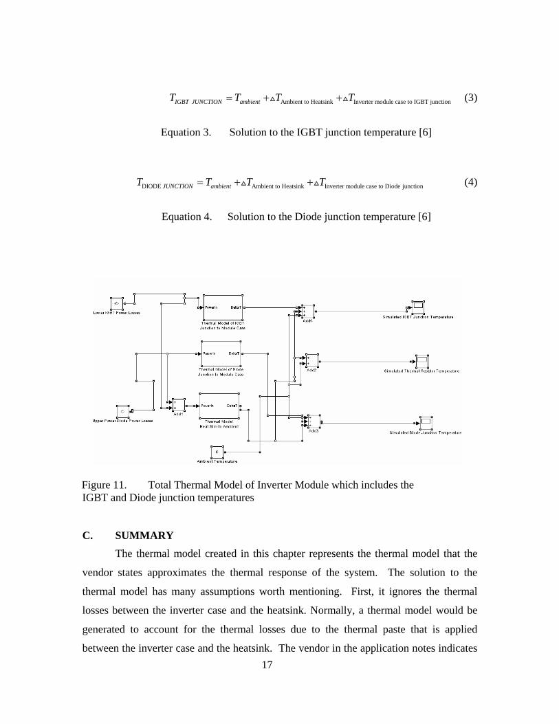
17
Ambient to Heatsink Inverter module case to IGBT junctionIGBT JUNCTION ambientT T T T= + + (3)
Equation 3. Solution to the IGBT junction temperature [6]
DIODE Ambient to Heatsink Inverter module case to Diode junctionJUNCTION ambientT T T T= + + (4)
Equation 4. Solution to the Diode junction temperature [6]
Figure 11. Total Thermal Model of Inverter Module which includes the IGBT and Diode junction temperatures
C. SUMMARY
The thermal model created in this chapter represents the thermal model that the
vendor states approximates the thermal response of the system. The solution to the
thermal model has many assumptions worth mentioning. First, it ignores the thermal
losses between the inverter case and the heatsink. Normally, a thermal model would be
generated to account for the thermal losses due to the thermal paste that is applied
between the inverter case and the heatsink. The vendor in the application notes indicates

18
that the thermal losses due to the thermal paste boundary are insignificant compared to
the other thermal losses. Second, the thermal coupling between the IGBT and the Diode
due to there close proximity is ignored because the vendor states that the thermal
coupling is minimal in the application notes. Instead of coupling, the application notes
suggest to use the hottest modeled semiconductor device junction temperature to be the
junction temperature of both devices. The relevancy and accuracy of these assumptions
will be further discussed in the simulations and conclusions chapters. In order to
compute the junction temperature using the thermal model developed in this chapter the
power losses must be computed. The power losses model is described and developed in
the next chapter.

19
III. POWER LOSSES MODEL
A. REASON FOR DEVELOPMENT
The power losses model was developed because the input required for the thermal
model created in chapter II is the average power dissipated by the semiconductor devices
in the VSI module. The simulation of thermal model is only made possible with power
data from a power losses model. After a successful thermal simulation, experimental
data will be collected in order to validate the thermal simulation data. After the
validation of the thermal model further simulation of the power losses and thermal
models will allow the research questions of Chapter I to be answered.
B. OVERVIEW To accurately predict and validate a thermal model of a VSI you must be able to
accurately predict the power losses of the system. In this thesis, a power losses model of
the semiconductor devices in the SKiiP 942GB120-317CTV was created in Simulink
using the vendor’s application notes and data given a valid electrical Simulink model of a
three phase VSI using PWM (see Appendix’s A) [6]. The power losses model was
experimentally compared to a controlled output of the VSI on a purely inductive load
with a 100 Vrms output.
The power losses of the semiconductor devices were divided into the static power
losses and the non-static power losses based on the vendors application notes [6]. The
static power losses were the on-state losses (conduction losses) and the blocking losses.
The non-static losses were divided into the switching losses (turn on/off) and driving
losses. The driving losses and blocking losses were neglected since they accounted for a
small portion of the overall power losses. An overview of the total power losses can be
seen in Figure 12 [6].

20
TOTAL POWER LOSSES
STATIC POWER LOSSES NON-STATIC POWER LOSSES
ON STATE POWER LOSSES BLOCKING POWER LOSSES SWITCHING POWER LOSSES DRIVING POWER LOSSES
TURN ON POWER LOSSES TURN OFF POWER LOSSESREVERSE RECOVERY POWER LOSSES
Figure 12. Overview and Breakdown of Total Power Losses[From 6]
C. DEVELOPMENT OF POWER LOSSES MODEL
1. Static Power Losses The first step in development of a power losses model was the development of a
validated electrical model. Since this thesis focuses on the power losses and thermal
models it is noted that without a validated electrical model of the VSI the power losses
model and thermal model couldn’t have been implemented. The electrical model will
only be referenced in order to clarify the power losses modeling. With that being said the
static power losses are made up of the on-state power losses (conduction losses) and the
blocking losses.
21
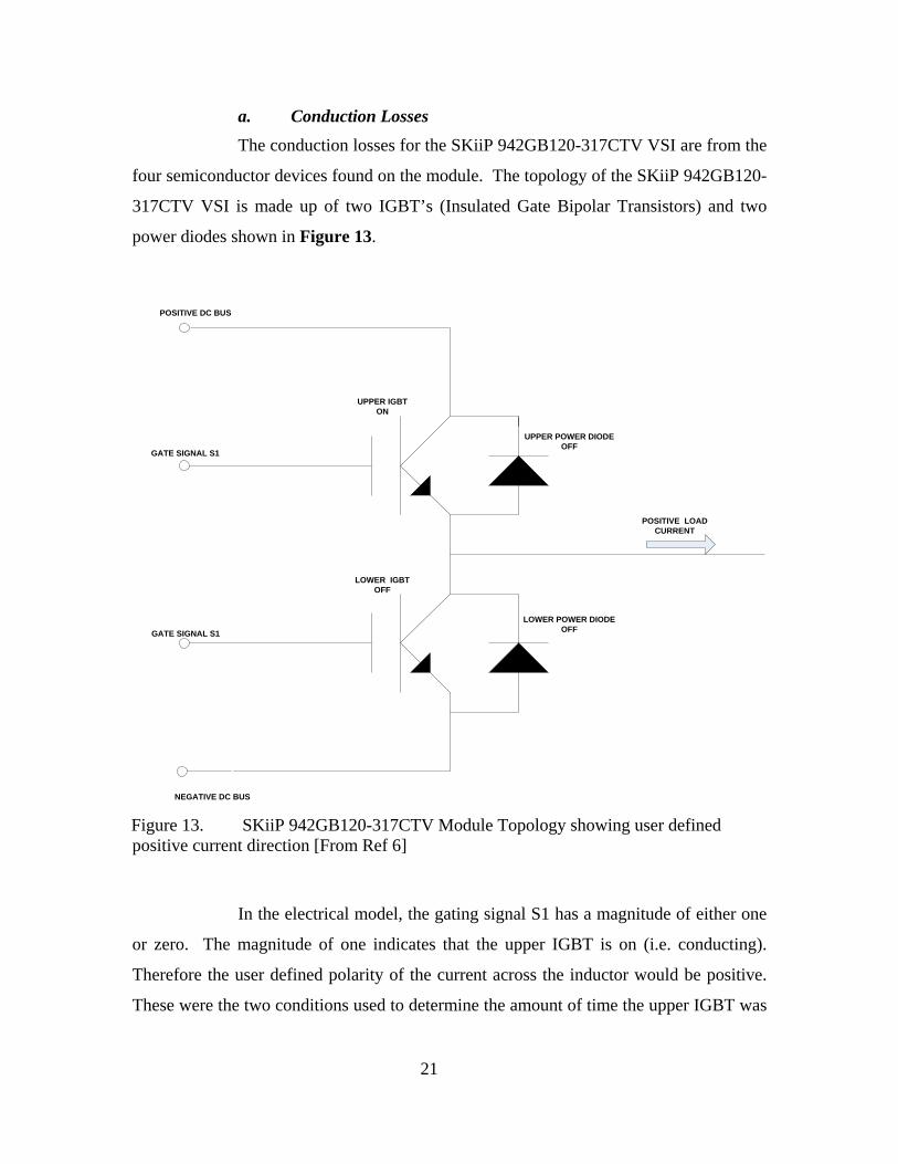
a. Conduction Losses
The conduction losses for the SKiiP 942GB120-317CTV VSI are from the
four semiconductor devices found on the module. The topology of the SKiiP 942GB120-
317CTV VSI is made up of two IGBT’s (Insulated Gate Bipolar Transistors) and two
power diodes shown in Figure 13.
UPPER IGBTON
LOWER IGBTOFF
UPPER POWER DIODEOFF
GATE SIGNAL S1
GATE SIGNAL S1
POSITIVE LOAD CURRENT
POSITIVE DC BUS
LOWER POWER DIODEOFF
NEGATIVE DC BUS Figure 13. SKiiP 942GB120-317CTV Module Topology showing user defined positive current direction [From Ref 6]
In the electrical model, the gating signal S1 has a magnitude of either one
or zero. The magnitude of one indicates that the upper IGBT is on (i.e. conducting).
Therefore the user defined polarity of the current across the inductor would be positive.
These were the two conditions used to determine the amount of time the upper IGBT was
22
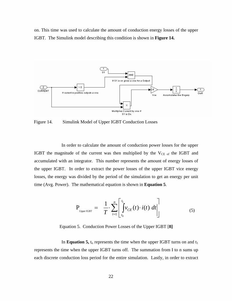
on. This time was used to calculate the amount of conduction energy losses of the upper
IGBT. The Simulink model describing this condition is shown in Figure 14.
Figure 14. Simulink Model of Upper IGBT Conduction Losses
In order to calculate the amount of conduction power losses for the upper
IGBT the magnitude of the current was then multiplied by the VCE of the IGBT and
accumulated with an integrator. This number represents the amount of energy losses of
the upper IGBT. In order to extract the power losses of the upper IGBT vice energy
losses, the energy was divided by the period of the simulation to get an energy per unit
time (Avg. Power). The mathematical equation is shown in Equation 5.
1
Upper IGBT
01
1P ( ) ( ) tn
CEi t
v t i t dtT =
⎡ ⎤= ⋅ ⋅⎢ ⎥
⎢ ⎥⎣ ⎦∑ ∫ (5)
Equation 5. Conduction Power Losses of the Upper IGBT [8]
In Equation 5, to represents the time when the upper IGBT turns on and t1
represents the time when the upper IGBT turns off. The summation from I to n sums up
each discrete conduction loss period for the entire simulation. Lastly, in order to extract
23
the amount of power losses from the upper IGBT vice energy losses the energy losses are
divided by the simulation time to give a energy per unit time (Avg. Power).
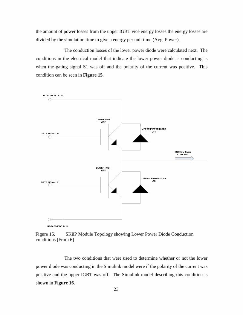
The conduction losses of the lower power diode were calculated next. The
conditions in the electrical model that indicate the lower power diode is conducting is
when the gating signal S1 was off and the polarity of the current was positive. This
condition can be seen in Figure 15.
Figure 15. SKiiP Module Topology showing Lower Power Diode Conduction conditions [From 6]
The two conditions that were used to determine whether or not the lower
power diode was conducting in the Simulink model were if the polarity of the current was
positive and the upper IGBT was off. The Simulink model describing this condition is
shown in Figure 16.

24
Figure 16. Simulink Model of Lower Power Diode Conduction Losses
In order to calculate the amount of conduction power losses for the lower
power diode the magnitude of the current was then multiplied by the VEC of the lower
power diode and accumulated with an integrator. This number represents the amount of
energy. In order to extract the power losses vice energy losses, the energy was divided
by the period of the simulation to get an energy per unit time (Power). The mathematical
equation is shown below in Equation 6.
1
Lower Power DIODE
01
1P ( ) ( ) tn
ECi t
v t i t dtT =
⎡ ⎤= ⋅ ⋅⎢ ⎥
⎢ ⎥⎣ ⎦∑ ∫ (6)
Equation 6. Conduction Power Losses Calculation for Lower Power Diode [8]
In Equation 6, to represents the time when the lower power diode turns on
and t1 represents the time when the lower power diode turns off. The summation from I
to n sums up each discrete lower power diode conduction loss period for the entire
simulation. Lastly, in order to extract the amount of conduction power losses from the
lower power diode vice energy losses the energy losses are divided by the simulation
time to give a energy per unit time (Avg. Power).
The conduction losses of the lower IGBT were calculated next. The
conditions of the Semikron VSI electrical model built in Simulink that indicate a lower

25
IGBT is conducting is when the gating signal S1 was 0 indicating the bottom IGBT was
on and the polarity of the current was negative. This condition can be seen in Figure 17.
Figure 17. Electrical Model of SKiiP Module Topology showing user defined negative current direction [From 6].
In the electrical model the gating signal S1 has a magnitude of either 1 or
0. The magnitude of 0 indicates that the lower IGBT is on (i.e. conducting). Therefore
the polarity of the current across the inductor would be negative. These were the two
conditions used to determine the amount of time the lower IGBT was on. The Simulink
model describing this condition is shown in Figure 18.
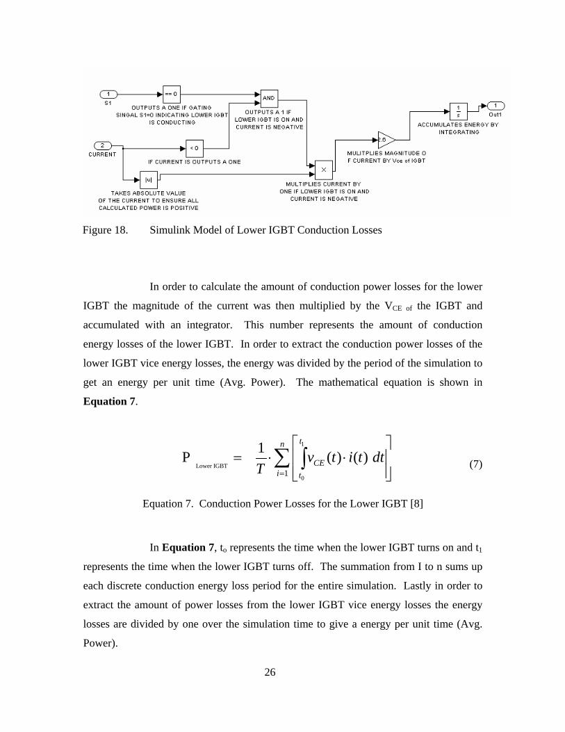
26
Figure 18. Simulink Model of Lower IGBT Conduction Losses
In order to calculate the amount of conduction power losses for the lower
IGBT the magnitude of the current was then multiplied by the VCE of the IGBT and
accumulated with an integrator. This number represents the amount of conduction
energy losses of the lower IGBT. In order to extract the conduction power losses of the
lower IGBT vice energy losses, the energy was divided by the period of the simulation to
get an energy per unit time (Avg. Power). The mathematical equation is shown in
Equation 7.
1
Lower IGBT
01
1P ( ) ( ) tn
CEi t
v t i t dtT =
⎡ ⎤= ⋅ ⋅⎢ ⎥
⎢ ⎥⎣ ⎦∑ ∫ (7)
Equation 7. Conduction Power Losses for the Lower IGBT [8]
In Equation 7, to represents the time when the lower IGBT turns on and t1
represents the time when the lower IGBT turns off. The summation from I to n sums up
each discrete conduction energy loss period for the entire simulation. Lastly in order to
extract the amount of power losses from the lower IGBT vice energy losses the energy
losses are divided by one over the simulation time to give a energy per unit time (Avg.
Power).
27
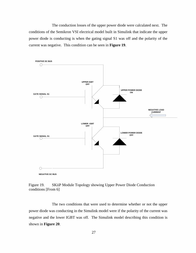
The conduction losses of the upper power diode were calculated next. The
conditions of the Semikron VSI electrical model built in Simulink that indicate the upper
power diode is conducting is when the gating signal S1 was off and the polarity of the
current was negative. This condition can be seen in Figure 19.
UPPER IGBTOFF
LOWER IGBTOFF
UPPER POWER DIODEON
GATE SIGNAL S1
GATE SIGNAL S1
NEGATIVE LOAD CURRENT
POSITIVE DC BUS
LOWER POWER DIODEOFF
NEGATIVE DC BUS
Figure 19. SKiiP Module Topology showing Upper Power Diode Conduction conditions [From 6]
The two conditions that were used to determine whether or not the upper
power diode was conducting in the Simulink model were if the polarity of the current was
negative and the lower IGBT was off. The Simulink model describing this condition is
shown in Figure 20.
28
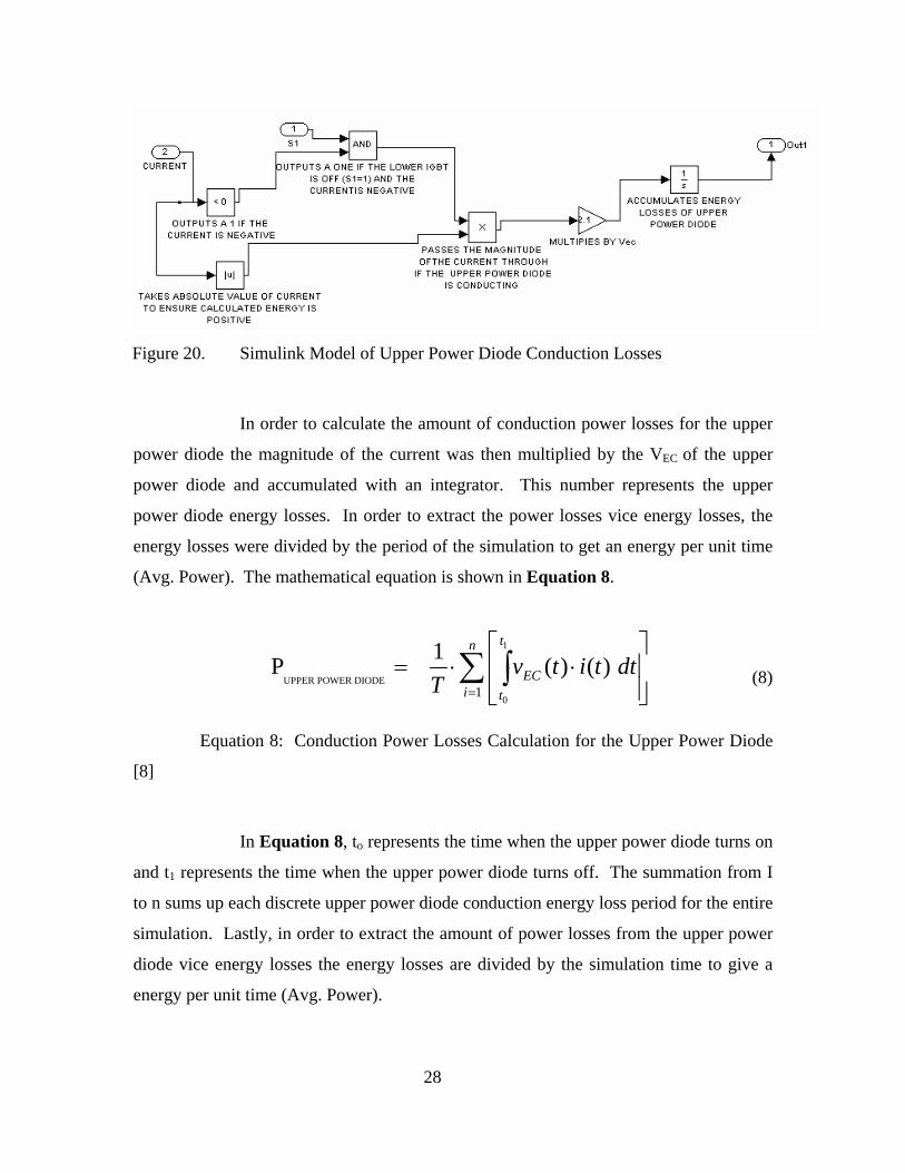
Figure 20. Simulink Model of Upper Power Diode Conduction Losses
In order to calculate the amount of conduction power losses for the upper
power diode the magnitude of the current was then multiplied by the VEC of the upper
power diode and accumulated with an integrator. This number represents the upper
power diode energy losses. In order to extract the power losses vice energy losses, the
energy losses were divided by the period of the simulation to get an energy per unit time
(Avg. Power). The mathematical equation is shown in Equation 8.
1
UPPER POWER DIODE
01
1P ( ) ( ) tn
ECi t
v t i t dtT =
⎡ ⎤= ⋅ ⋅⎢ ⎥
⎢ ⎥⎣ ⎦∑ ∫ (8)
Equation 8: Conduction Power Losses Calculation for the Upper Power Diode
[8]
In Equation 8, to represents the time when the upper power diode turns on
and t1 represents the time when the upper power diode turns off. The summation from I
to n sums up each discrete upper power diode conduction energy loss period for the entire
simulation. Lastly, in order to extract the amount of power losses from the upper power
diode vice energy losses the energy losses are divided by the simulation time to give a
energy per unit time (Avg. Power).
29
b. Blocking Losses
The blocking losses for this thesis will be neglected. The hypothesis is
that the amount of forward blocking losses will be orders of magnitude smaller than the
conduction losses, turn on/off losses, and reverse recovery losses. This hypothesis is
based on the given vendor data sheets and application notes supplied from Semikron for
the VSI modeled for this thesis.
2. Non-Static Power Losses
The non-static power losses are made up of the switching power losses and the
driver power losses for the IGBT’s. The switching power losses are made up of the turn
on/ off losses of the upper and lower IGBT and the reverse recovery losses as the diode
junctions transition from a reverse biased state to a forward biased state.
a. Turn on/off Losses for the Upper IGBT The turn on/off losses for upper IGBT were calculated using the given
data sheet from Semikron for the SKiiP 942GB120-317CTV (Appendix A). In order to
calculate the amount of turn on/off cycles of the upper IGBT a rise detector was created
in Simulink for the gating signal S1. Since the Semikron gave a value for the amount of
energy per turn on/off cycle it was only necessary to count the entire event. Therefore the
number of turn on events equaled the number of turn off events which was equal to the
number of rise detects. The way to determine whether or not it was the upper IGBT
turning on or off was to verify that the rise event happened while the current was
positive. Therefore the two conditions required to count the number of turn on/off events
for the upper IGBT was to count the number of rise events with the current being positive
assuming that for every turn on event there was a turn off event. The value of the turn
on/off losses was given by the vendor in the data sheet (see Appendix A) was related to a
maximum current and voltage. In order to scale the turn on/off losses for the actual used
voltage and current two gains were used.
The first gain block takes the absolute value of the current and multiplies
it by the turn on/off losses and then divides it by the maximum value of current
referenced in the vendor data sheet (See Appendix A). The second gain block takes the

30
current scaled turn on/off losses out of gain block one and multiplies it by the Vdc and
then divides it by the maximum value of voltage referenced in the vendor data sheet (See
Appendix A). The Simulink model coded for this event is shown in Figure 21. The
Simulink model detects switching events of the upper IGBT and adds a current and
voltage scaled turn on/off energy losses which is accumulated for the entire simulation
period. The mathematical equation describing the calculation of the upper IGBT turn
on/off Power losses is shown in Equation 9.
Figure 21. Simulink Model of Upper IGBT Turn On/Off Power Losses
( ) ( )UPPER IGBTTURN ON/OFFPOWER LOSSES
3
1
225*101P * *750 600
ndc
i
Vi
T
−
=
⎡ ⎤⎢ ⎥= ⋅⎢ ⎥⎣ ⎦
∑ (9)
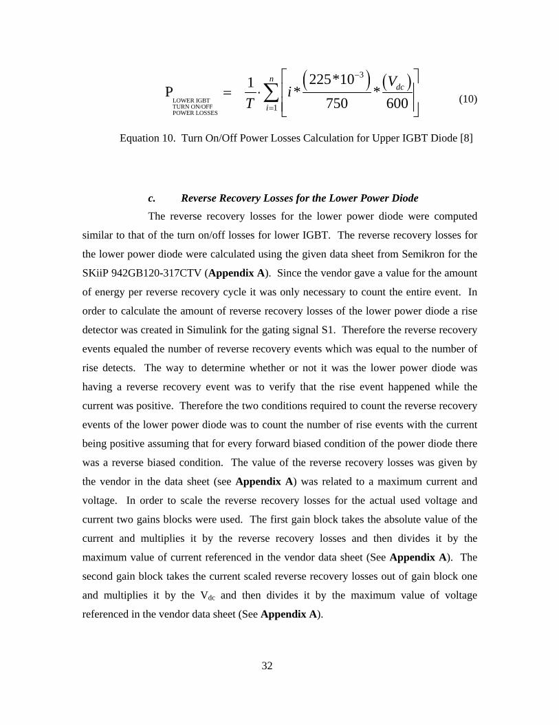
Equation 9: Turn On/Off Power Losses Calculation for Upper IGBT Diode [8]
b. Turn on/off Losses for the Lower IGBT
The turn on/off losses for lower IGBT were calculated using the given
data sheet from Semikron for the SKiiP 942GB120-317CTV (Appendix A). In order to
calculate the amount of turn on/off cycles of the lower IGBT a rise detector was created
in Simulink for the gating signal S1. Since the Semikron gave a value for the amount of

31
energy per turn on/off cycle it was only necessary to count the entire event. Therefore
the number of turn on events equaled the number of turn off events which was equal to
the number of rise detects. The way to determine whether or not it was the lower IGBT
turning on or off was to verify that the rise event happened while the current was
negative. Therefore the two conditions required to count the number of turn on/off
events for the lower IGBT was to count the number of rise events with the current being
negative assuming that for every turn on event there was a turn off event. The value of
the turn on/off losses was given by the vendor in the data sheet (see Appendix A) was
related to a maximum current and voltage. In order to scale the turn on/off losses for the
actual used voltage and current two gains were used. The first gain block takes the
absolute value of the current and multiplies it by the turn on/off losses and then divides it
by the maximum value of current referenced in the vendor data sheet (See Appendix A).
The second gain block takes the current scaled turn on/off losses out of gain block one
and multiplies it by the Vdc and then divides it by the maximum value of voltage
referenced in the vendor data sheet (See Appendix A).
The Simulink model coded for this event is shown in Figure 22. The
Simulink model detects switching events of the lower IGBT and adds a current and
voltage scaled turn on/off energy losses which is accumulated for the entire simulation
period. The mathematical equation describing the calculation of the lower IGBT turn
on/off Power losses is shown in Equation 10.
Figure 22. Simulink Model of Lower IGBT Turn On/Off Power Losses
32
( ) ( )LOWER IGBTTURN ON/OFFPOWER LOSSES
3
1
225*101P * *750 600
ndc
i
Vi
T
−
=
⎡ ⎤⎢ ⎥= ⋅⎢ ⎥⎣ ⎦
∑ (10)
Equation 10. Turn On/Off Power Losses Calculation for Upper IGBT Diode [8]
c. Reverse Recovery Losses for the Lower Power Diode The reverse recovery losses for the lower power diode were computed
similar to that of the turn on/off losses for lower IGBT. The reverse recovery losses for
the lower power diode were calculated using the given data sheet from Semikron for the
SKiiP 942GB120-317CTV (Appendix A). Since the vendor gave a value for the amount
of energy per reverse recovery cycle it was only necessary to count the entire event. In
order to calculate the amount of reverse recovery losses of the lower power diode a rise
detector was created in Simulink for the gating signal S1. Therefore the reverse recovery
events equaled the number of reverse recovery events which was equal to the number of
rise detects. The way to determine whether or not it was the lower power diode was
having a reverse recovery event was to verify that the rise event happened while the
current was positive. Therefore the two conditions required to count the reverse recovery
events of the lower power diode was to count the number of rise events with the current
being positive assuming that for every forward biased condition of the power diode there
was a reverse biased condition. The value of the reverse recovery losses was given by
the vendor in the data sheet (see Appendix A) was related to a maximum current and
voltage. In order to scale the reverse recovery losses for the actual used voltage and
current two gains blocks were used. The first gain block takes the absolute value of the
current and multiplies it by the reverse recovery losses and then divides it by the
maximum value of current referenced in the vendor data sheet (See Appendix A). The
second gain block takes the current scaled reverse recovery losses out of gain block one
and multiplies it by the Vdc and then divides it by the maximum value of voltage
referenced in the vendor data sheet (See Appendix A).

33
The Simulink model coded for this event is shown in Figure 23. The
Simulink model detects reverse recovery events of the lower power diode and
accumulates a current and voltage scaled reverse recovery energy losses for the entire
simulation period. The mathematical equation describing the calculation of the lower
power diode reverse recovery Power losses is shown in Equation 11.
Figure 23. Simulink Model of Lower Power Diode Reverse Recovery Power Losses
( ) ( )LOWER POWERDIODE REVERSERECOVERY POWER LOSSES
3
1
30*101P * *750 600
ndc
i
Vi
T
−
=
⎡ ⎤⎢ ⎥= ⋅⎢ ⎥⎣ ⎦
∑ (11)
Equation 11. Reverse Recovery Power Losses Calculation for Lower Power Diode [8]
d. Reverse Recovery Losses for the Upper Power Diode
The reverse recovery losses for the upper power diode were computed
similar to that of the turn on/off losses for upper IGBT. The reverse recovery losses for
the upper power diode were calculated using the given data sheet from Semikron for the
SKiiP 942GB120-317CTV (Appendix A). Since the vendor gave a value for the amount

34
of energy per reverse recovery cycle it was only necessary to count the entire event. In
order to calculate the amount of reverse recovery losses of the upper power diode a rise
detector was created in Simulink for the gating signal S1. Therefore the reverse recovery
events equaled the number of reverse recovery events which was equal to the number of
rise detects. The way to determine whether or not it was the upper power diode was
having a reverse recovery event was to verify that the rise event happened while the
current was negative. Therefore the two conditions required to count the reverse
recovery events of the upper power diode was to count the number of rise events with the
current being negative assuming that for every forward biased condition of the power
diode there was a reverse biased condition. The value of the reverse recovery losses was
given by the vendor in the data sheet (see Appendix A) was related to a maximum
current and voltage. In order to scale the reverse recovery losses for the actual used
voltage and current two gains blocks were used. The first gain block takes the absolute
value of the current and multiplies it by the reverse recovery losses and then divides it by
the maximum value of current referenced in the vendor data sheet (See Appendix A).
The second gain block takes the current scaled reverse recovery losses out of gain block
one and multiplies it by the Vdc and then divides it by the maximum value of voltage
referenced in the vendor data sheet (See Appendix A).
The Simulink model coded for this event is shown in Figure 24. The
Simulink model detects reverse recovery events of the upper power diode and
accumulates a current and voltage scaled reverse recovery energy losses for the entire
simulation period. The mathematical equation describing the calculation of the upper
power diode reverse recovery Power losses is shown in Equation 12.

35
Figure 24. Simulink Model of Upper Power Diode Reverse Recovery Power Losses
( ) ( )UPPER POWERDIODE REVERSERECOVERY POWER LOSSES
3
1
30*101P * *750 600
ndc
i
Vi
T
−
=
⎡ ⎤⎢ ⎥= ⋅⎢ ⎥⎣ ⎦
∑ (12)
Equation 12. Reverse Recovery Power Losses Calculation for Lower Power
Diode [8]
e. Driving Power Losses The driving losses for this thesis will be neglected. The hypothesis is that
the amount of driver losses will be orders of magnitude smaller than the conduction
losses, turn on/off losses, and reverse recovery losses. This hypothesis is based on the
given data sheets and application notes supplied from Semikron for the 3 phase VSI
modeled for this thesis.
D. CREATING A THREE PHASE VSI POWER LOSSES MODEL The entire description so far only described the modeling of power losses of one
Semikron SKiiP 942GB120-317CTV inverter pole separately. The model of all the
power losses of one inverter pole is shown in Figure 25. The outputs of each individual
type of power losses were summed together and all power losses of one IGBT and its
corresponding diode were outputted to the workspace in Matlab for input to the thermal

36
model. The thermal model only requires the power losses one IGBT and its
corresponding power diode. The rest of the power losses model was built to resemble the
experimental equipment in the lab. The system in the lab consisted of three Semikron
SKiiP 942GB120-317CTV connected as a three phase VSI DC-AC. The other two
phases were modeled identically to the phase that has been described. The output of all
energy from the three phases of voltage source inverter were then summed together and
divided by the simulation time in order to produce the total power losses and is shown in
the Simulink model(Figure 26).
Figure 25. Simulink Model of Summation of Power Losses for one SKiiP 942GB120-317CTV VSI
37
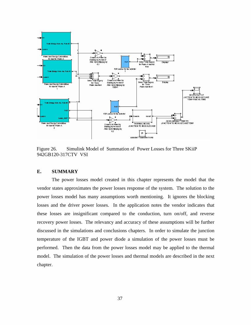
Figure 26. Simulink Model of Summation of Power Losses for Three SKiiP 942GB120-317CTV VSI
E. SUMMARY The power losses model created in this chapter represents the model that the
vendor states approximates the power losses response of the system. The solution to the
power losses model has many assumptions worth mentioning. It ignores the blocking
losses and the driver power losses. In the application notes the vendor indicates that
these losses are insignificant compared to the conduction, turn on/off, and reverse
recovery power losses. The relevancy and accuracy of these assumptions will be further
discussed in the simulations and conclusions chapters. In order to simulate the junction
temperature of the IGBT and power diode a simulation of the power losses must be
performed. Then the data from the power losses model may be applied to the thermal
model. The simulation of the power losses and thermal models are described in the next
chapter.

38
THIS PAGE INTENTIONALLY LEFT BLANK
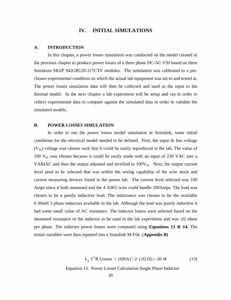
39
IV. INITIAL SIMULATIONS
A. INTRODUCTION
In this chapter, a power losses simulation was conducted on the model created in
the previous chapter to produce power losses of a three phase DC-AC VSI based on three
Semikron SKiiP 942GB120-317CTV modules. The simulation was calibrated to a pre-
chosen experimental condition on which the actual lab equipment was set to and tested at.
The power losses simulation data will then be collected and used as the input to the
thermal model. In the next chapter a lab experiment will be setup and ran in order to
collect experimental data to compare against the simulated data in order to validate the
simulated models.
B. POWER LOSSES SIMULATION In order to run the power losses model simulation in Simulink, some initial
conditions for the electrical model needed to be defined. First, the input dc bus voltage
(Vdc) voltage was chosen such that it could be easily reproduced in the lab. The value of
100 Vdc was chosen because it could be easily made with an input of 230 VAC into a
VARIAC and then the output adjusted and rectified to 100Vdc. Next, the output current
level need to be selected that was within the wiring capability of the wire stock and
current measuring devices found in the power lab. The current level selected was 100
Amps since it both measured and the 4 AWG wire could handle 100Amps. The load was
chosen to be a purely inductive load. The inductance was chosen to be the available
0.30mH 3 phase inductors available in the lab. Although the load was purely inductive it
had some small value of AC resistance. The inductor losses were selected based on the
measured resistance of the inductor to be used in the lab experiment and was .02 ohms
per phase. The inductor power losses were computed using Equations 13 & 14. The
initial variables were then inputted into a Simulink M-File. (Appendix B)
^2L I R Losses = (100A) ^ 2 (.02 ) 20 Wφ ⋅ Ω = (13)
Equation 13. Power Losses Calculation Single Phase Inductor

40
^23L I R Losses =3 (20W)=60 Wφ ⋅ (14)
Equation 14. Power Losses Calculation for Three Phase Inductor
The next step was to run the simulation with the lab calibrated input values. The
output of the simulation is seen in Figure 27. The results of the simulation were that for
the Semikron three phase VSI using PWM at a switching frequency of 5 kHz with an
input voltage of 100Vdc and a output current of 100A and output voltage of 100 VAC at
60Hz, the total power losses were 635.7 Watts as seen in Figure 27. The Outputs of the
IGBT and its corresponding diode extracted out of there respective subsystems as shown
in Figure 28&29. In the next section, the power losses of one IGBT and its
corresponding diode are placed in the thermal model created in Chapter II.
Figure 27. Simulink Simulation of Power Losses for Semikron Three Phase VSI

41
Figure 28. Simulink Simulation Showing 65.6 Watts of Power Losses for Lower IGBT
Figure 29. Simulink Simulation of 35.5 Watts of Power Losses for Upper Power Diode

42
C. THERMAL MODEL SIMULATION
In order to run the thermal model simulation in Simulink, some initial conditions
for the thermal model from the Semikron data sheets (Appendix A) needed to be defined
and are shown in Table 1. Also since the heatsink used was the water cooled heatsink
(NWK 40) the thermal resistance of the heatsink was calculated by assuming a given
flow rate of 5.3l/min and a Rth of 0.018 °C/W (Figure 30). This rate was chosen after
determining that the available equipment in the lab could support this flow rate for the
experimental data collection. After the thermal model was calibrated, the average power
of the IGBT and diode collected in the previous section were placed into the thermal
model by exporting them to Matlab workspace as variables to be used by the thermal
model.
%Thermal Model Initial Variables
%IGBT junction to Case Variables Rthi1=3 Rthi2=2 Rthi3=4 Rthi4=0 tau_i1=1
tau_i2=0.13 tau_i3=0.001 tau_i4=0
% Diode junction to Case Variables Rthd1=9 Rthd2=64 Rthd3=10 Rthd4=0 tau_d1=1
tau_d2=0.13 tau_d4=0
%Heatsink to Ambient Variables Rthhx1=0.018 tau_hx1=100
%Ambient Temperature ambient_temp=25.5
Table 1. List of initial Variables for Thermal Model.
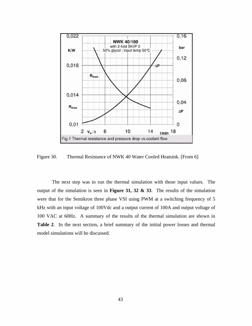
43
Figure 30. Thermal Resistance of NWK 40 Water Cooled Heatsink. [From 6]
The next step was to run the thermal simulation with those input values. The
output of the simulation is seen in Figure 31, 32 & 33. The results of the simulation
were that for the Semikron three phase VSI using PWM at a switching frequency of 5
kHz with an input voltage of 100Vdc and a output current of 100A and output voltage of
100 VAC at 60Hz. A summary of the results of the thermal simulation are shown in
Table 2. In the next section, a brief summary of the initial power losses and thermal
model simulations will be discussed.
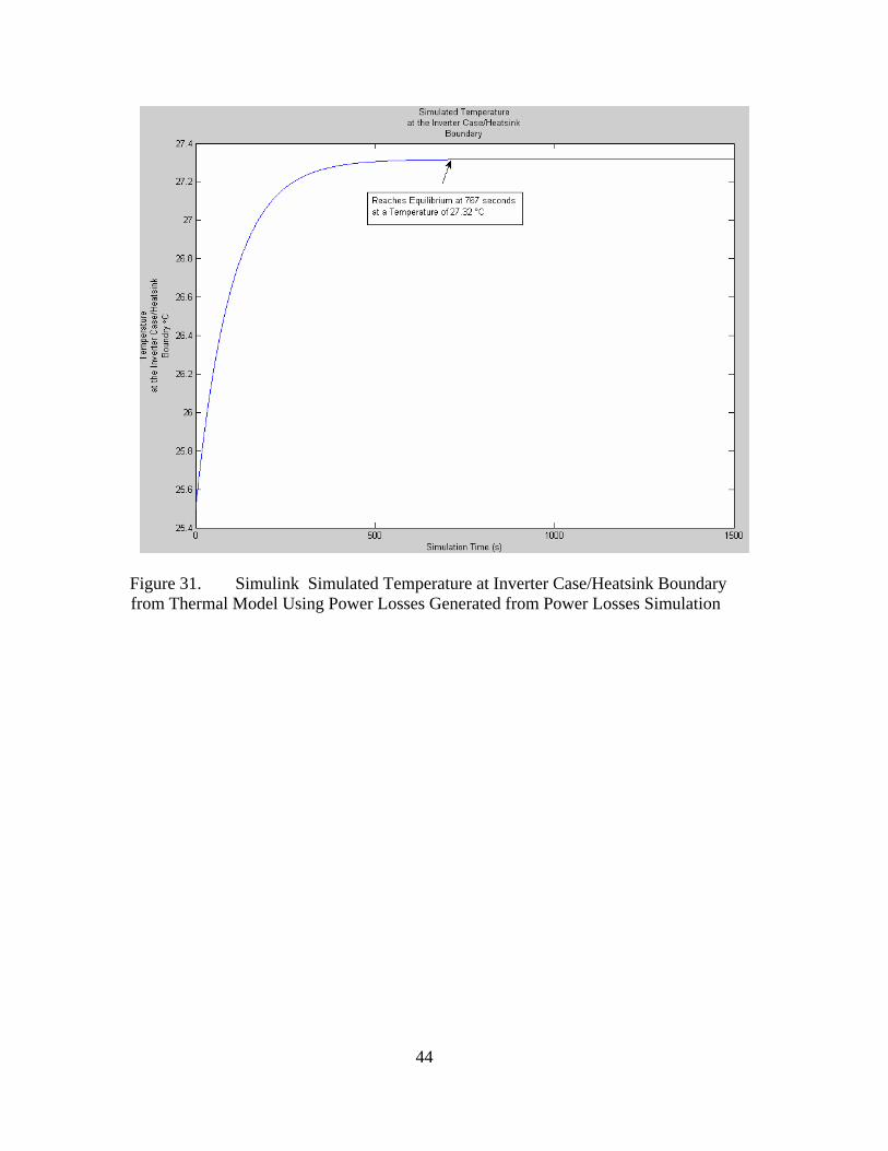
44
Figure 31. Simulink Simulated Temperature at Inverter Case/Heatsink Boundary from Thermal Model Using Power Losses Generated from Power Losses Simulation

45
Figure 32. Simulink Simulated IGBT Junction Temperature from Thermal Model Using Power Losses Generated from Power Losses Simulation

46
Figure 33. Simulink Simulated Diode Junction Temperature from Thermal Model Using Power Losses Generated from Power Losses Simulation
Simulated
IGBT
Junction
Temperature
Simulated
Diode Junction
Temperature
Simulated
Temperature at
Inverter
Case/Heatsink
Boundary
Final Simulation
Temperature 27.91°C 30.25 °C 27.32 °C
Time till
Equilibrium
(seconds)
715 560 767
Table 2. Summary of Simulated Temperatures of a Semikron Skip Semikron three phase
VSI using PWM at a switching frequency of 5 kHz with an input voltage of 100Vdc, output current of 100A, and an output voltage of 100 VAC at 60Hz with an ambient temperature of 25.5°C.
47
D. SUMMARY
The results of the initial simulation show an exponential build up function with a
rising temperature that reaches equilibrium at around 700 seconds which was the
expected response. The unexpected result obtained was that the diode junction
temperature was higher than that of the IGBT junction even though the power losses of
the diode were less than that of the IGBT. The reason for this is the values of thermal
resistance in diode provided by the vendor (Appendix A) are greater than the thermal
resistances values of the IGBT. Since there time constants are identical it makes sense
that the one with the higher power isn’t necessary the one with the higher temperature
rise. Also the input voltage was low (100Vdc) compared to its maximum (350 Vdc) and
this also contributed to the diode temperature being hottest. In the next chapter, lab
equipment will be set up to match the simulation and experimental data will be collected
in order to validate the simulated models.

48
THIS PAGE INTENTIONALLY LEFT BLANK

49
V. EXPERIMENTAL DATA ACQUISTION
A. INTRODUCTION
In order to validate the simulated data of the power losses and thermal models a
DC-AC VSI inverter was setup as in the lab to match the simulated conditions. The
controller for the DC-AC VSI used a PWM scheme at 5 kHz just like the electrical model
did for the simulations. The VSI used was the Semikron SKiiP 942GB120-317CTV,
because the hardware was available in the lab. The setup of the experimental system
used for data collection is shown in a basic block diagram in Figure 34. The
experimental data will be collected in order to determine the heat capacity of the system
and also to validate the Simulink models. The heat capacity of the system will then be
used in order to find out how long it would take for system to shutdown on over
temperature protection on a loss of coolant casualty (LOCC).
B. CONSTRUCTION The construction of the three phase DC-AC VSI system in Figure 35 was
accomplished in three steps. First, the input power to the DC-AC VSI needed to be
created from available AC from the wall outlet. Next, the three phase inductive load
needed to be connected to output of phase A, B and C of the DC-AC VSI. Finally, the
measurement devices were added in order to monitor the DC input voltage and current
and the output voltage and current and the thermal resistor voltage representing IGBT
junction temperature. The wires that were chosen to connect the given components were
chosen based on 100 Amps of current. The 4 AWG wire was used since its current
capacity was in excess of 100 Amps.
1. Input Power
The input voltage required for the DC Bus of the VSI was created by taking three
phase 208VAC 60Hz from the wall outlet and applying it to a STATCO ENERGY
PRODUCTS CO. 12.1kVA VARIAC (Figure 36). The output of the VARIAC was
applied to a CRYDOM M-50 six pack diode rectifier which rectifies the output to DC.
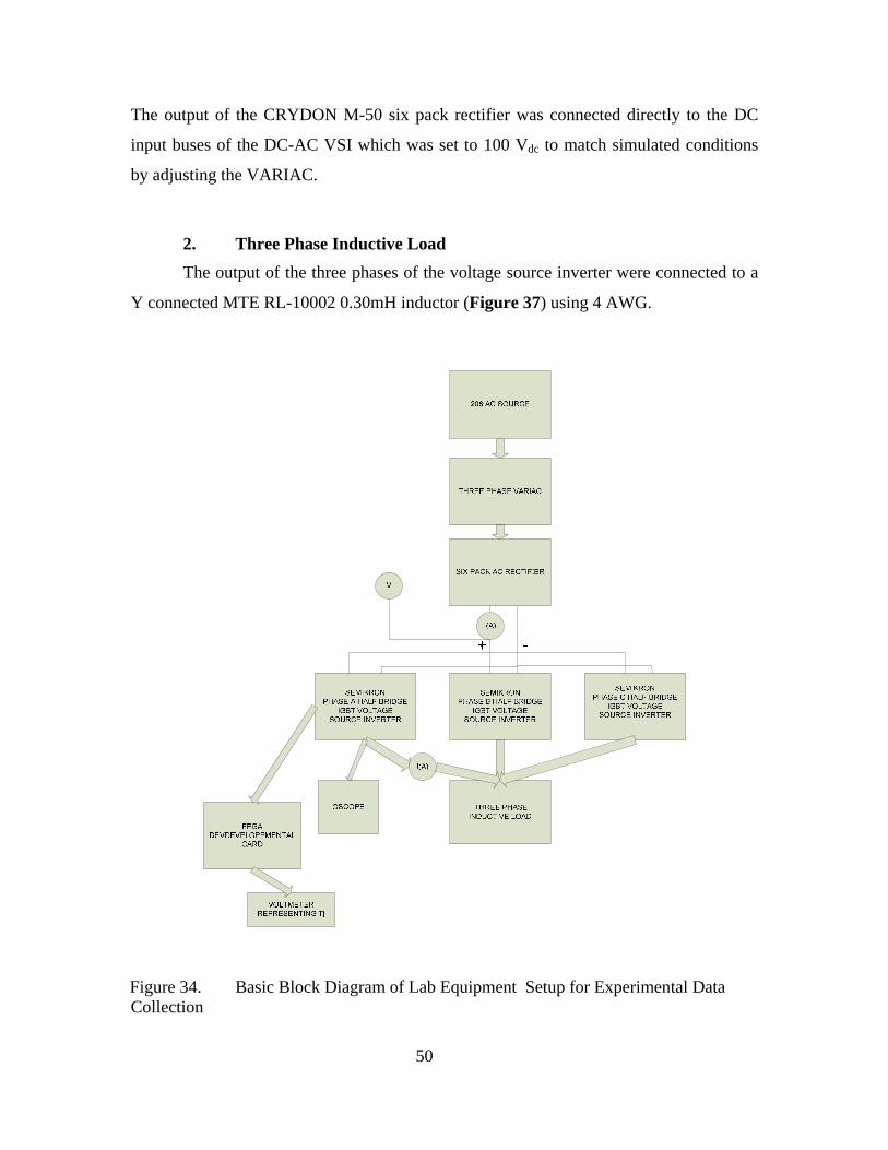
50
The output of the CRYDON M-50 six pack rectifier was connected directly to the DC
input buses of the DC-AC VSI which was set to 100 Vdc to match simulated conditions
by adjusting the VARIAC.
2. Three Phase Inductive Load The output of the three phases of the voltage source inverter were connected to a
Y connected MTE RL-10002 0.30mH inductor (Figure 37) using 4 AWG.
Figure 34. Basic Block Diagram of Lab Equipment Setup for Experimental Data Collection

51
3. Measurement Devices
The variables that needed to monitored and measured were the thermal resistor
voltage, dc input current, dc input voltage, ac output voltage and ac output current. The
output current of the CRYDOM six pack was measured with an AEMC SL206 AC/DC
current probe that was connected to a EXTECH INSTRUMENTS MultiMaster 560 True
RMS meter set to the VDC mode. The output of the current probe was a voltage that
represented the current level with a scaling factor of 10mv/A. The DC bus input voltage
was measured with a EXTECH INSTRUMENTS MultiMaster 560 True RMS set to the
VDC mode. The DC voltage that represented the junction temperature was routed from
the SKiiP module through the FPGA based controller card to a EXTECH
INSTRUMENTS MultiMaster 560 True RMS set to the VDC mode. The Load current
was measure with two TEXTRONIC AS6303 current probes. Two probes were required
since each one maximum capability was 50A. The Load Voltage was monitored and
recorded on a TEXTRONIC TDS 3012B Oscilloscope via a TEXTRONIC P5200 High
Voltage Differential Probe.
Volt-Meter Representing Thermal Resistor Temperature
representing IGBT Junction Temperature
Semikron SKiiP Module Semikron NWK 40
Water Cooled Heatsink
FPGA Based Controller Card Utilizing Pulse
Width Modulation and Relaying Thermal
Resistor Temperature from SKiiP Module to
Voltmeter
Figure 35. Semikron DC-AC VSI Module used for the 625KW Fuel Cell and Reformer Demonstration Set Up to Match Simulink Models

52
Figure 36. STATCO ENERGY PRODUCTS CO. 12.1kVA VARIAC
Figure 37. Y Connected MTE RL-10002 0.30mH Inductor

53
C. DATA COLLECTION
The experimental VSI system was connected as previously discussed and the
controller card was programmed in order to get a current of 100Arms and a voltage
100Vrms. Next, all measuring equipment was calibrated and current probes were
degaussed. Two data runs were completed. The first data run was run without any
coolant flow to the heat exchanger. This data set will be used to determine the heat
capacity of the system and later determine how long it would take for the system to
shutdown on over temperature protection on a loss of coolant casualty. The second data
run was run with cooling water applied to the heat sink in order to validate the simulated
power losses and thermal models data.
1. First Data Run with No Coolant Flow Conducted on 08Jun05
The controller card was configured to provide a load current of 100 Arms and a
load voltage of 100 Vrms. The DC bus was set to 51 VDC by adjusting the VARIAC and
the measured DC bus current was 12.6Amps which was measured on an AEMC SL206
AC/DC current probe that was connected to a EXTECH INSTRUMENTS MultiMaster
560 True RMS meter set to the VDC mode. The actual voltage that was measured was
126mV with a scaling factor of 10mV/A was 12.6Amps. The DC Bus voltage was
measured with a EXTECH INSTRUMENTS MultiMaster 560 True RMS meter set to the
VDC mode measured 51VDC. The Output Current was measured with two TEXTRONIC
AS6303 current probes that were inputted to the two channels of a TEXTRONIC TDS
3012B Oscilloscope and summed together using the summing function. Two current
probes were used because the value of current was above 100Amps which was the rating
of each individually current probe. The load voltage was measured to be 100VAC and is
shown in Figure 38 calculated in Equation 15. The current was measure to be 100
Amps shown in Figure 39 and calculated in Equation 16. The ambient room
temperature was recorded to be 24°C with a BRAUN SS CO. CAT. No. 610 Laboratory
Grade Thermometer. The experimental time was measured with a SEIKO ARCTURA
stopwatch. The thermal data was collected and recorded every thirty seconds for 125
minutes and is shown in Table 3.
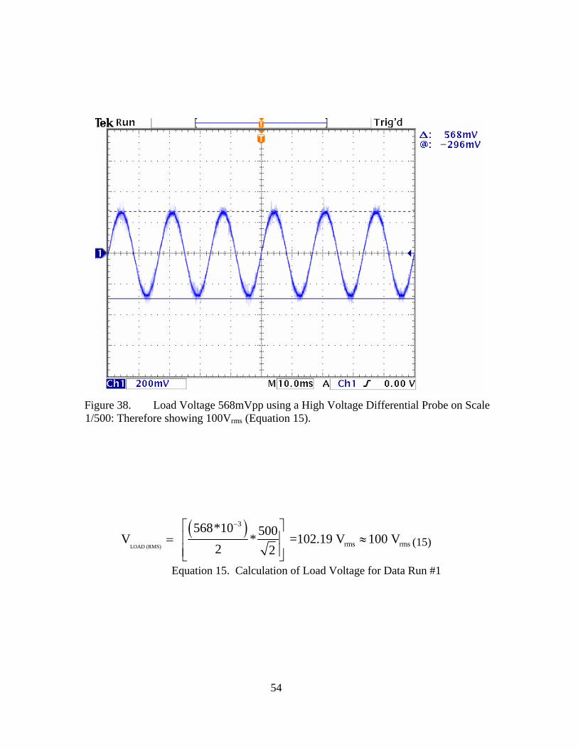
54
Figure 38. Load Voltage 568mVpp using a High Voltage Differential Probe on Scale 1/500: Therefore showing 100Vrms (Equation 15).
( )LOAD (RMS)
3
rms rms
568*10 500V * =102.19 V 100 V2 2
−⎡ ⎤⎢ ⎥= ≈⎢ ⎥⎣ ⎦
(15)
Equation 15. Calculation of Load Voltage for Data Run #1
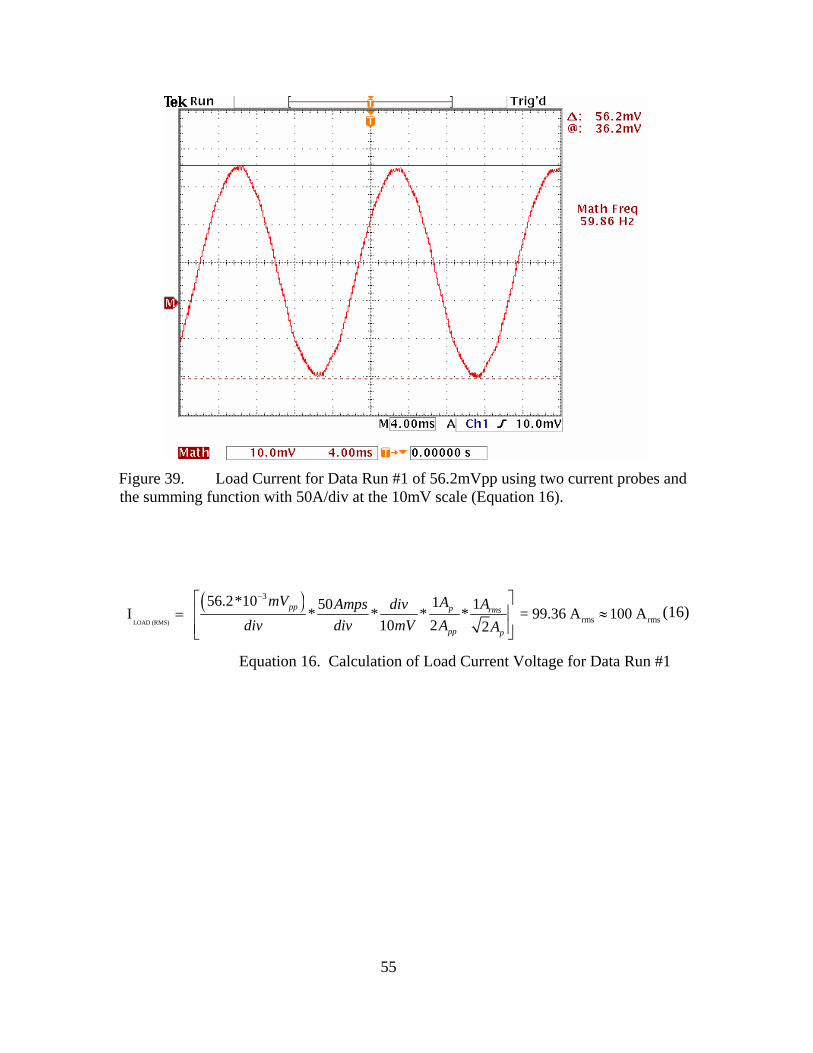
55
Figure 39. Load Current for Data Run #1 of 56.2mVpp using two current probes and the summing function with 50A/div at the 10mV scale (Equation 16).
( )LOAD (RMS)
3
rms rms
56.2*10 1 150I * * * * = 99.36 A 100 A10 2 2
pp p rms
pp p
mV A AAmps divdiv div mV A A
−⎡ ⎤⎢ ⎥= ≈⎢ ⎥⎣ ⎦
(16)
Equation 16. Calculation of Load Current Voltage for Data Run #1
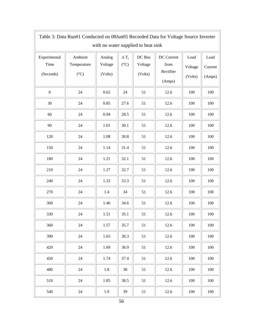
56
Table 3: Data Run#1 Conducted on 08Jun05 Recorded Data for Voltage Source Inverter
with no water supplied to heat sink
Experimental
Time
(Seconds)
Ambient
Temperature
(°C)
Analog
Voltage
(Volts)
∆ Tj
(°C)
DC Bus
Voltage
(Volts)
DC Current
from
Rectifier
(Amps)
Load
Voltage
(Volts)
Load
Current
(Amps)
0 24 0.62 24 51 12.6 100 100
30 24 0.85 27.6 51 12.6 100 100
60 24 0.94 28.5 51 12.6 100 100
90 24 1.01 30.1 51 12.6 100 100
120 24 1.08 30.8 51 12.6 100 100
150 24 1.14 31.4 51 12.6 100 100
180 24 1.21 32.1 51 12.6 100 100
210 24 1.27 32.7 51 12.6 100 100
240 24 1.33 33.3 51 12.6 100 100
270 24 1.4 34 51 12.6 100 100
300 24 1.46 34.6 51 12.6 100 100
330 24 1.51 35.1 51 12.6 100 100
360 24 1.57 35.7 51 12.6 100 100
390 24 1.63 36.3 51 12.6 100 100
420 24 1.69 36.9 51 12.6 100 100
450 24 1.74 37.4 51 12.6 100 100
480 24 1.8 38 51 12.6 100 100
510 24 1.85 38.5 51 12.6 100 100
540 24 1.9 39 51 12.6 100 100

57
Table 3: Data Run#1 Conducted on 08Jun05 Recorded Data for Voltage Source Inverter
with no water supplied to heat sink
Experimental
Time
(Seconds)
Ambient
Temperature
(°C)
Analog
Voltage
(Volts)
∆ Tj
(°C)
DC Bus
Voltage
(Volts)
DC Current
from
Rectifier
(Amps)
Load
Voltage
(Volts)
Load
Current
(Amps)
570 24 1.95 39.5 51 12.6 100 100
600 24 2 40 51 12.6 100 100
630 24 2.06 40.6 51 12.6 100 100
660 24 2.11 41.1 51 12.6 100 100
690 24 2.16 41.6 51 12.6 100 100
720 24 2.21 42.1 51 12.6 100 100
750 24 2.26 42.6 51 12.6 100 100
780 24 2.3 43 51 12.6 100 100
810 24 2.35 43.5 51 12.6 100 100
840 24 2.4 44 51 12.6 100 100
870 24 2.44 44.4 51 12.6 100 100
900 24 2.49 44.9 51 12.6 100 100
930 24 2.53 45.3 51 12.6 100 100
960 24 2.58 45.8 51 12.6 100 100
990 24 2.62 46.2 51 12.6 100 100
1020 24 2.66 46.6 51 12.6 100 100
1050 24 2.71 47.1 51 12.6 100 100
1080 24 2.75 47.5 51 12.6 100 100
1110 24 2.79 47.9 51 12.6 100 100

58
Table 3: Data Run#1 Conducted on 08Jun05 Recorded Data for Voltage Source Inverter
with no water supplied to heat sink
Experimental
Time
(Seconds)
Ambient
Temperature
(°C)
Analog
Voltage
(Volts)
∆ Tj
(°C)
DC Bus
Voltage
(Volts)
DC Current
from
Rectifier
(Amps)
Load
Voltage
(Volts)
Load
Current
(Amps)
1140 24 2.83 48.3 51 12.6 100 100
1170 24 2.87 48.7 51 12.6 100 100
1200 24 2.91 49.1 51 12.6 100 100
1230 24 2.95 49.5 51 12.6 100 100
1260 24 2.99 49.9 51 12.6 100 100
1290 24 3.03 50.3 51 12.6 100 100
1320 24 3.07 50.7 51 12.6 100 100
1350 24 3.1 51 51 12.6 100 100
1380 24 3.14 51.4 51 12.6 100 100
1410 24 3.18 51.8 51 12.6 100 100
1440 24 3.21 52.1 51 12.6 100 100
1470 24 3.25 52.5 51 12.6 100 100
1500 24 3.29 52.9 51 12.6 100 100
1530 24 3.32 53.2 51 12.6 100 100
1560 24 3.36 53.6 51 12.6 100 100
1590 24 3.39 53.9 51 12.6 100 100
1620 24 3.42 54.2 51 12.6 100 100
1650 24 3.45 54.5 51 12.6 100 100
1680 24 3.49 54.9 51 12.6 100 100
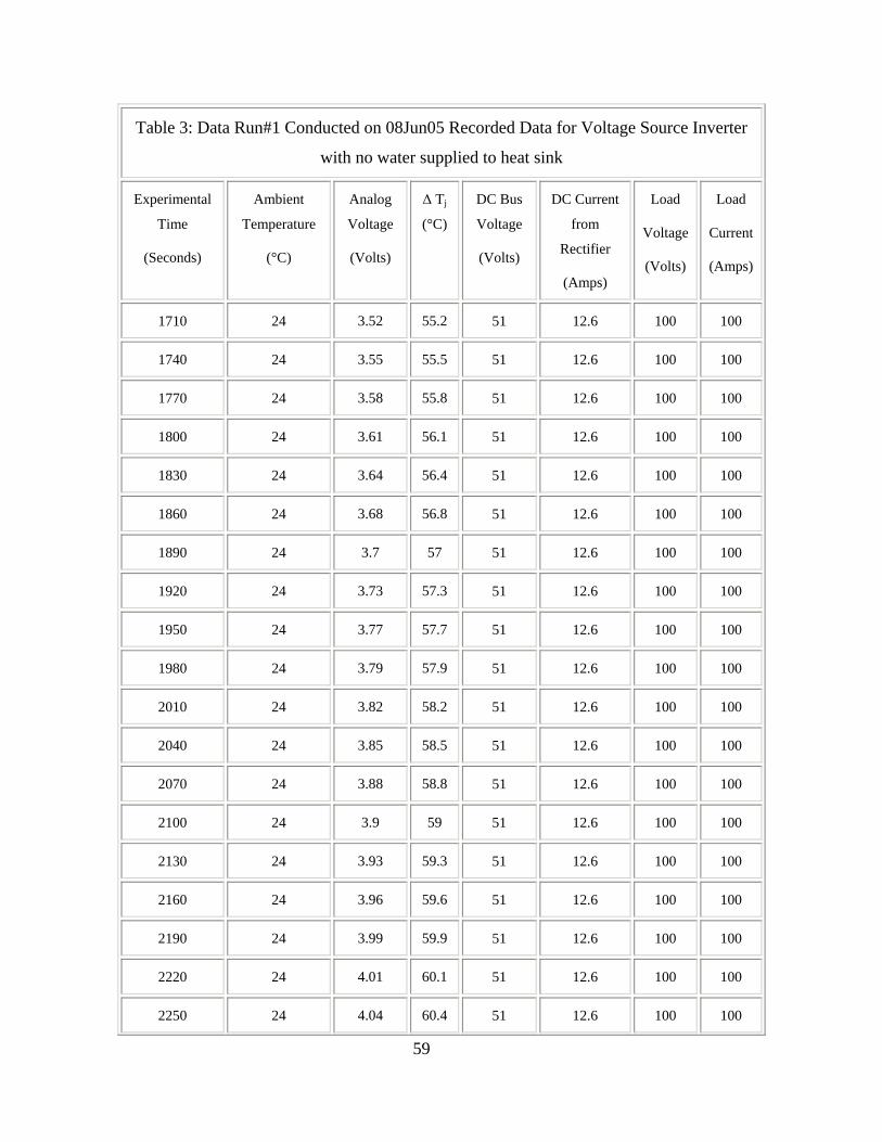
59
Table 3: Data Run#1 Conducted on 08Jun05 Recorded Data for Voltage Source Inverter
with no water supplied to heat sink
Experimental
Time
(Seconds)
Ambient
Temperature
(°C)
Analog
Voltage
(Volts)
∆ Tj
(°C)
DC Bus
Voltage
(Volts)
DC Current
from
Rectifier
(Amps)
Load
Voltage
(Volts)
Load
Current
(Amps)
1710 24 3.52 55.2 51 12.6 100 100
1740 24 3.55 55.5 51 12.6 100 100
1770 24 3.58 55.8 51 12.6 100 100
1800 24 3.61 56.1 51 12.6 100 100
1830 24 3.64 56.4 51 12.6 100 100
1860 24 3.68 56.8 51 12.6 100 100
1890 24 3.7 57 51 12.6 100 100
1920 24 3.73 57.3 51 12.6 100 100
1950 24 3.77 57.7 51 12.6 100 100
1980 24 3.79 57.9 51 12.6 100 100
2010 24 3.82 58.2 51 12.6 100 100
2040 24 3.85 58.5 51 12.6 100 100
2070 24 3.88 58.8 51 12.6 100 100
2100 24 3.9 59 51 12.6 100 100
2130 24 3.93 59.3 51 12.6 100 100
2160 24 3.96 59.6 51 12.6 100 100
2190 24 3.99 59.9 51 12.6 100 100
2220 24 4.01 60.1 51 12.6 100 100
2250 24 4.04 60.4 51 12.6 100 100
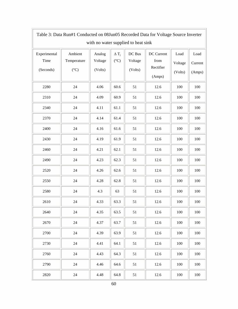
60
Table 3: Data Run#1 Conducted on 08Jun05 Recorded Data for Voltage Source Inverter
with no water supplied to heat sink
Experimental
Time
(Seconds)
Ambient
Temperature
(°C)
Analog
Voltage
(Volts)
∆ Tj
(°C)
DC Bus
Voltage
(Volts)
DC Current
from
Rectifier
(Amps)
Load
Voltage
(Volts)
Load
Current
(Amps)
2280 24 4.06 60.6 51 12.6 100 100
2310 24 4.09 60.9 51 12.6 100 100
2340 24 4.11 61.1 51 12.6 100 100
2370 24 4.14 61.4 51 12.6 100 100
2400 24 4.16 61.6 51 12.6 100 100
2430 24 4.19 61.9 51 12.6 100 100
2460 24 4.21 62.1 51 12.6 100 100
2490 24 4.23 62.3 51 12.6 100 100
2520 24 4.26 62.6 51 12.6 100 100
2550 24 4.28 62.8 51 12.6 100 100
2580 24 4.3 63 51 12.6 100 100
2610 24 4.33 63.3 51 12.6 100 100
2640 24 4.35 63.5 51 12.6 100 100
2670 24 4.37 63.7 51 12.6 100 100
2700 24 4.39 63.9 51 12.6 100 100
2730 24 4.41 64.1 51 12.6 100 100
2760 24 4.43 64.3 51 12.6 100 100
2790 24 4.46 64.6 51 12.6 100 100
2820 24 4.48 64.8 51 12.6 100 100

61
Table 3: Data Run#1 Conducted on 08Jun05 Recorded Data for Voltage Source Inverter
with no water supplied to heat sink
Experimental
Time
(Seconds)
Ambient
Temperature
(°C)
Analog
Voltage
(Volts)
∆ Tj
(°C)
DC Bus
Voltage
(Volts)
DC Current
from
Rectifier
(Amps)
Load
Voltage
(Volts)
Load
Current
(Amps)
2850 24 4.5 65 51 12.6 100 100
2880 24 4.52 65.2 51 12.6 100 100
2910 24 4.54 65.4 51 12.6 100 100
2940 24 4.56 65.6 51 12.6 100 100
2970 24 4.58 65.8 51 12.6 100 100
3000 24 4.6 66 51 12.6 100 100
3030 24 4.62 66.2 51 12.6 100 100
3060 24 4.64 66.4 51 12.6 100 100
3090 24 4.65 66.5 51 12.6 100 100
3120 24 4.67 66.7 51 12.6 100 100
3150 24 4.69 66.9 51 12.6 100 100
3180 24 4.71 67.1 51 12.6 100 100
3210 24 4.73 67.3 51 12.6 100 100
3240 24 4.74 67.4 51 12.6 100 100
3270 24 4.76 67.6 51 12.6 100 100
3300 24 4.78 67.8 51 12.6 100 100
3330 24 4.8 68 51 12.6 100 100
3360 24 4.81 68.1 51 12.6 100 100
3390 24 4.83 68.3 51 12.6 100 100
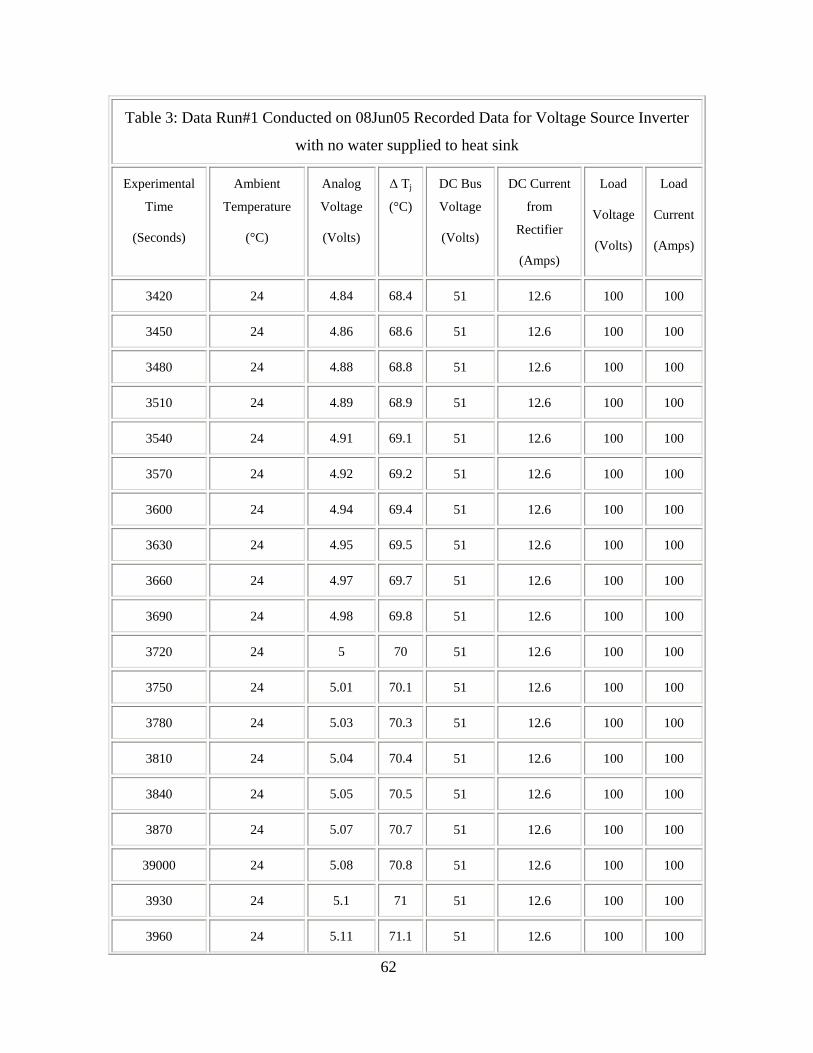
62
Table 3: Data Run#1 Conducted on 08Jun05 Recorded Data for Voltage Source Inverter
with no water supplied to heat sink
Experimental
Time
(Seconds)
Ambient
Temperature
(°C)
Analog
Voltage
(Volts)
∆ Tj
(°C)
DC Bus
Voltage
(Volts)
DC Current
from
Rectifier
(Amps)
Load
Voltage
(Volts)
Load
Current
(Amps)
3420 24 4.84 68.4 51 12.6 100 100
3450 24 4.86 68.6 51 12.6 100 100
3480 24 4.88 68.8 51 12.6 100 100
3510 24 4.89 68.9 51 12.6 100 100
3540 24 4.91 69.1 51 12.6 100 100
3570 24 4.92 69.2 51 12.6 100 100
3600 24 4.94 69.4 51 12.6 100 100
3630 24 4.95 69.5 51 12.6 100 100
3660 24 4.97 69.7 51 12.6 100 100
3690 24 4.98 69.8 51 12.6 100 100
3720 24 5 70 51 12.6 100 100
3750 24 5.01 70.1 51 12.6 100 100
3780 24 5.03 70.3 51 12.6 100 100
3810 24 5.04 70.4 51 12.6 100 100
3840 24 5.05 70.5 51 12.6 100 100
3870 24 5.07 70.7 51 12.6 100 100
39000 24 5.08 70.8 51 12.6 100 100
3930 24 5.1 71 51 12.6 100 100
3960 24 5.11 71.1 51 12.6 100 100
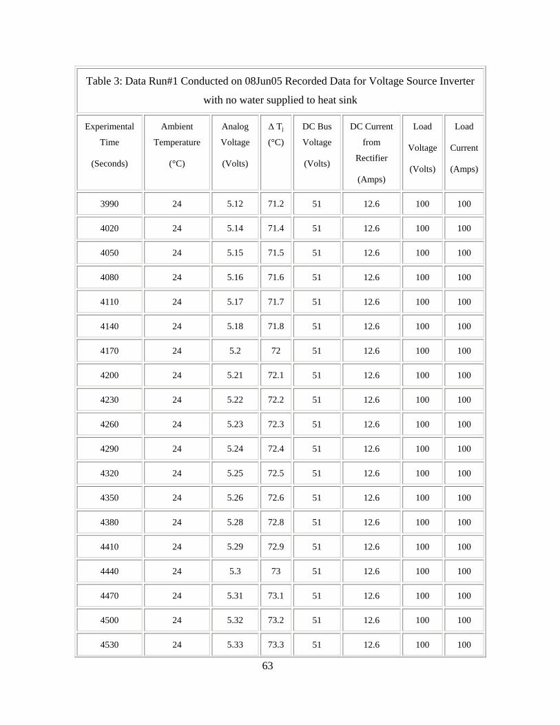
63
Table 3: Data Run#1 Conducted on 08Jun05 Recorded Data for Voltage Source Inverter
with no water supplied to heat sink
Experimental
Time
(Seconds)
Ambient
Temperature
(°C)
Analog
Voltage
(Volts)
∆ Tj
(°C)
DC Bus
Voltage
(Volts)
DC Current
from
Rectifier
(Amps)
Load
Voltage
(Volts)
Load
Current
(Amps)
3990 24 5.12 71.2 51 12.6 100 100
4020 24 5.14 71.4 51 12.6 100 100
4050 24 5.15 71.5 51 12.6 100 100
4080 24 5.16 71.6 51 12.6 100 100
4110 24 5.17 71.7 51 12.6 100 100
4140 24 5.18 71.8 51 12.6 100 100
4170 24 5.2 72 51 12.6 100 100
4200 24 5.21 72.1 51 12.6 100 100
4230 24 5.22 72.2 51 12.6 100 100
4260 24 5.23 72.3 51 12.6 100 100
4290 24 5.24 72.4 51 12.6 100 100
4320 24 5.25 72.5 51 12.6 100 100
4350 24 5.26 72.6 51 12.6 100 100
4380 24 5.28 72.8 51 12.6 100 100
4410 24 5.29 72.9 51 12.6 100 100
4440 24 5.3 73 51 12.6 100 100
4470 24 5.31 73.1 51 12.6 100 100
4500 24 5.32 73.2 51 12.6 100 100
4530 24 5.33 73.3 51 12.6 100 100

64
Table 3: Data Run#1 Conducted on 08Jun05 Recorded Data for Voltage Source Inverter
with no water supplied to heat sink
Experimental
Time
(Seconds)
Ambient
Temperature
(°C)
Analog
Voltage
(Volts)
∆ Tj
(°C)
DC Bus
Voltage
(Volts)
DC Current
from
Rectifier
(Amps)
Load
Voltage
(Volts)
Load
Current
(Amps)
4560 24 5.34 73.4 51 12.6 100 100
4590 24 5.35 73.5 51 12.6 100 100
4620 24 5.36 73.6 51 12.6 100 100
4650 24 5.37 73.7 51 12.6 100 100
4680 24 5.38 73.8 51 12.6 100 100
4710 24 5.39 73.9 51 12.6 100 100
4740 24 5.4 74 51 12.6 100 100
4770 24 5.41 74.1 51 12.6 100 100
4800 24 5.42 74.2 51 12.6 100 100
4830 24 5.43 74.3 51 12.6 100 100
4860 24 5.44 74.4 51 12.6 100 100
4890 24 5.45 74.5 51 12.6 100 100
4920 24 5.45 74.5 51 12.6 100 100
4950 24 5.46 74.6 51 12.6 100 100
4980 24 5.47 74.7 51 12.6 100 100
5010 24 5.48 74.8 51 12.6 100 100
5040 24 5.49 74.9 51 12.6 100 100
5070 24 5.5 75 51 12.6 100 100
5100 24 5.51 75.1 51 12.6 100 100
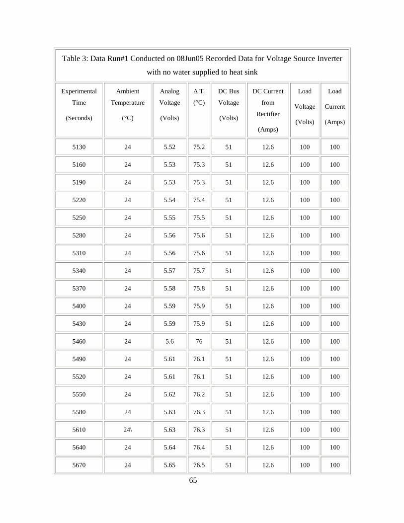
65
Table 3: Data Run#1 Conducted on 08Jun05 Recorded Data for Voltage Source Inverter
with no water supplied to heat sink
Experimental
Time
(Seconds)
Ambient
Temperature
(°C)
Analog
Voltage
(Volts)
∆ Tj
(°C)
DC Bus
Voltage
(Volts)
DC Current
from
Rectifier
(Amps)
Load
Voltage
(Volts)
Load
Current
(Amps)
5130 24 5.52 75.2 51 12.6 100 100
5160 24 5.53 75.3 51 12.6 100 100
5190 24 5.53 75.3 51 12.6 100 100
5220 24 5.54 75.4 51 12.6 100 100
5250 24 5.55 75.5 51 12.6 100 100
5280 24 5.56 75.6 51 12.6 100 100
5310 24 5.56 75.6 51 12.6 100 100
5340 24 5.57 75.7 51 12.6 100 100
5370 24 5.58 75.8 51 12.6 100 100
5400 24 5.59 75.9 51 12.6 100 100
5430 24 5.59 75.9 51 12.6 100 100
5460 24 5.6 76 51 12.6 100 100
5490 24 5.61 76.1 51 12.6 100 100
5520 24 5.61 76.1 51 12.6 100 100
5550 24 5.62 76.2 51 12.6 100 100
5580 24 5.63 76.3 51 12.6 100 100
5610 24\ 5.63 76.3 51 12.6 100 100
5640 24 5.64 76.4 51 12.6 100 100
5670 24 5.65 76.5 51 12.6 100 100

66
Table 3: Data Run#1 Conducted on 08Jun05 Recorded Data for Voltage Source Inverter
with no water supplied to heat sink
Experimental
Time
(Seconds)
Ambient
Temperature
(°C)
Analog
Voltage
(Volts)
∆ Tj
(°C)
DC Bus
Voltage
(Volts)
DC Current
from
Rectifier
(Amps)
Load
Voltage
(Volts)
Load
Current
(Amps)
5700 24 5.66 76.6 51 12.6 100 100
5730 24 5.66 76.6 51 12.6 100 100
5760 24 5.66 76.6 51 12.6 100 100
5790 24 5.67 76.7 51 12.6 100 100
5820 24 5.68 76.8 51 12.6 100 100
5850 24 5.68 76.8 51 12.6 100 100
5880 24 5.69 76.9 51 12.6 100 100
5910 24 5.69 76.9 51 12.6 100 100
5940 24 5.7 77 51 12.6 100 100
5970 24 5.7 77 51 12.6 100 100
6000 24 5.71 77.1 51 12.6 100 100
6030 24 5.71 77.1 51 12.6 100 100
6060 24 5.72 77.2 51 12.6 100 100
6090 24 5.72 77.2 51 12.6 100 100
6120 24 5.73 77.3 51 12.6 100 100
6150 24 5.74 77.4 51 12.6 100 100
6180 24 5.74 77.4 51 12.6 100 100
6210 24 5.75 77.5 51 12.6 100 100
6240 24 5.76 77.6 51 12.6 100 100
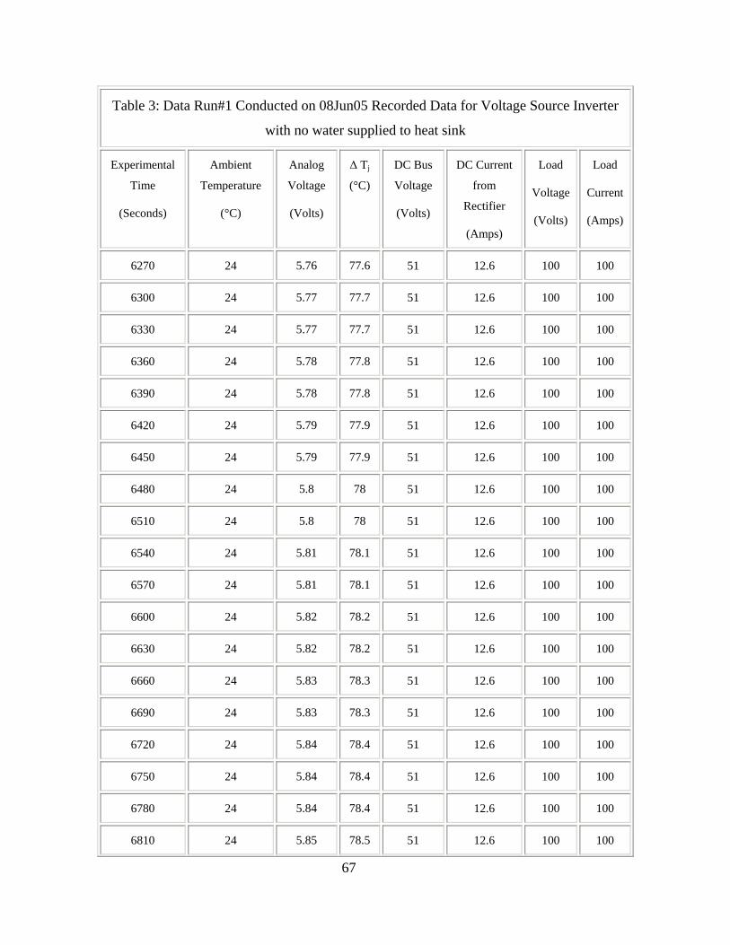
67
Table 3: Data Run#1 Conducted on 08Jun05 Recorded Data for Voltage Source Inverter
with no water supplied to heat sink
Experimental
Time
(Seconds)
Ambient
Temperature
(°C)
Analog
Voltage
(Volts)
∆ Tj
(°C)
DC Bus
Voltage
(Volts)
DC Current
from
Rectifier
(Amps)
Load
Voltage
(Volts)
Load
Current
(Amps)
6270 24 5.76 77.6 51 12.6 100 100
6300 24 5.77 77.7 51 12.6 100 100
6330 24 5.77 77.7 51 12.6 100 100
6360 24 5.78 77.8 51 12.6 100 100
6390 24 5.78 77.8 51 12.6 100 100
6420 24 5.79 77.9 51 12.6 100 100
6450 24 5.79 77.9 51 12.6 100 100
6480 24 5.8 78 51 12.6 100 100
6510 24 5.8 78 51 12.6 100 100
6540 24 5.81 78.1 51 12.6 100 100
6570 24 5.81 78.1 51 12.6 100 100
6600 24 5.82 78.2 51 12.6 100 100
6630 24 5.82 78.2 51 12.6 100 100
6660 24 5.83 78.3 51 12.6 100 100
6690 24 5.83 78.3 51 12.6 100 100
6720 24 5.84 78.4 51 12.6 100 100
6750 24 5.84 78.4 51 12.6 100 100
6780 24 5.84 78.4 51 12.6 100 100
6810 24 5.85 78.5 51 12.6 100 100

68
Table 3: Data Run#1 Conducted on 08Jun05 Recorded Data for Voltage Source Inverter
with no water supplied to heat sink
Experimental
Time
(Seconds)
Ambient
Temperature
(°C)
Analog
Voltage
(Volts)
∆ Tj
(°C)
DC Bus
Voltage
(Volts)
DC Current
from
Rectifier
(Amps)
Load
Voltage
(Volts)
Load
Current
(Amps)
6840 24 5.85 78.5 51 12.6 100 100
6870 24 5.86 78.6 51 12.6 100 100
6900 24 5.86 78.6 51 12.6 100 100
6930 24 5.86 78.6 51 12.6 100 100
6960 24 5.87 78.7 51 12.6 100 100
6990 24 5.87 78.7 51 12.6 100 100
7020 24 5.88 78.8 51 12.6 100 100
7050 24 5.88 78.8 51 12.6 100 100
7080 24 5.88 78.8 51 12.6 100 100
7110 24 5.89 78.9 51 12.6 100 100
7140 24 5.89 78.9 51 12.6 100 100
7170 24 5.89 78.9 51 12.6 100 100
7200 24 5.89 78.9 51 12.6 100 100
7230 24 5.9 79 51 12.6 100 100
7260 24 5.9 79 51 12.6 100 100
7290 24 5.91 79.1 51 12.6 100 100
7320 24 5.91 79.1 51 12.6 100 100
7350 24 5.91 79.1 51 12.6 100 100
7380 24 5.91 79.1 51 12.6 100 100
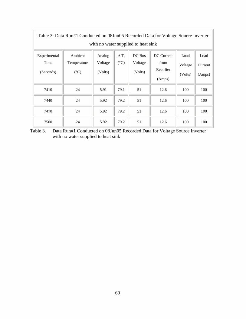
69
Table 3: Data Run#1 Conducted on 08Jun05 Recorded Data for Voltage Source Inverter
with no water supplied to heat sink
Experimental
Time
(Seconds)
Ambient
Temperature
(°C)
Analog
Voltage
(Volts)
∆ Tj
(°C)
DC Bus
Voltage
(Volts)
DC Current
from
Rectifier
(Amps)
Load
Voltage
(Volts)
Load
Current
(Amps)
7410 24 5.91 79.1 51 12.6 100 100
7440 24 5.92 79.2 51 12.6 100 100
7470 24 5.92 79.2 51 12.6 100 100
7500 24 5.92 79.2 51 12.6 100 100
Table 3. Data Run#1 Conducted on 08Jun05 Recorded Data for Voltage Source Inverter with no water supplied to heat sink

70
The plotted thermal resistor temperature for data run #1 is shown Figure 40.
Figure 40. Matlab Plot of Rise in Thermal Resistor Temperature with no coolant flow and input power of 642 Watts for Semikron Source Inverter SKiiP942GB120-317CTV with an ambient temperature of 24°C.
The experimental data plotted above correlates to the expected response of a
exponential buildup function. The above data was then used to determine the time
constant of the entire thermal system based on the first order thermal model of the system
(Figure 41) [6].
Figure 41. Thermal Model Approximation of 1st Order System [6].
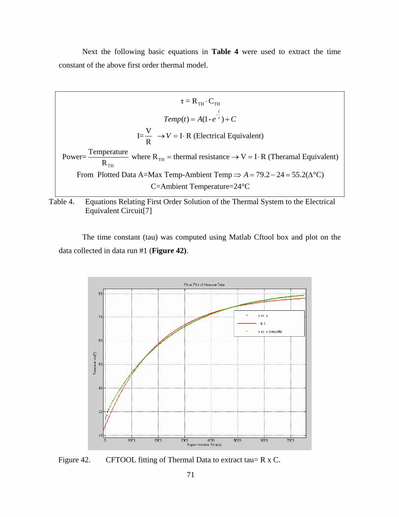
71
Next the following basic equations in Table 4 were used to extract the time
constant of the above first order thermal model.
TH TH
-
THTH
τ = R C
( ) (1- )VI= I R (Electrical Equivalent)R
TemperaturePower= where R thermal resistance V I R (Theramal Equivalent)R
From Plotted Data A=Max Temp-Ambient Temp 79.2 24 55.2(
t
Temp t A e C
V
A
τ
⋅
= +
→ = ⋅
= → = ⋅
⇒ = − = °C)C=Ambient Temperature=24°C
∆
Table 4. Equations Relating First Order Solution of the Thermal System to the Electrical Equivalent Circuit[7]
The time constant (tau) was computed using Matlab Cftool box and plot on the
data collected in data run #1 (Figure 42).
Figure 42. CFTOOL fitting of Thermal Data to extract tau= R x C.
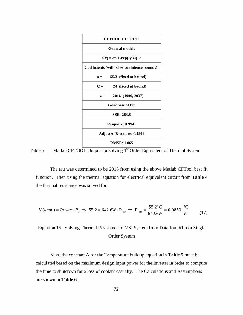
72
CFTOOL OUTPUT:
General model:
f(y) = a*(1-exp(-y/z))+c
Coefficients (with 95% confidence bounds):
a = 55.3 (fixed at bound)
C = 24 (fixed at bound)
z = 2018 (1999, 2037)
Goodness of fit:
SSE: 283.8
R-square: 0.9941
Adjusted R-square: 0.9941
RMSE: 1.065
Table 5. Matlab CFTOOL Output for solving 1st Order Equivalent of Thermal System
The tau was determined to be 2018 from using the above Matlab CFTool best fit
function. Then using the thermal equation for electrical equivalent circuit from Table 4
the thermal resistance was solved for.
TH TH55.2°C °C( ) 55.2 642.6 R R 0.0859 642.6thV temp Power R W
W W= ⋅ ⇒ = ⋅ ⇒ = = (17)
Equation 15. Solving Thermal Resistance of VSI System from Data Run #1 as a Single
Order System
Next, the constant A for the Temperature buildup equation in Table 5 must be
calculated based on the maximum design input power for the inverter in order to compute
the time to shutdown for a loss of coolant casualty. The Calculations and Assumptions
are shown in Table 6.
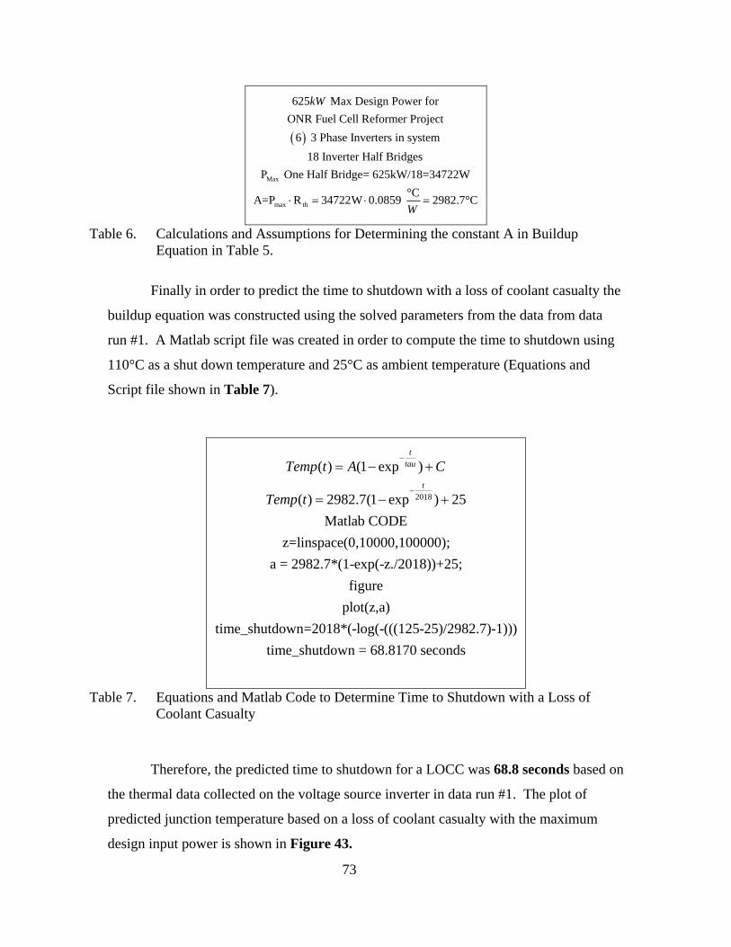
73
( )
Max
max th
625 Max Design Power forONR Fuel Cell Reformer Project
6 3 Phase Inverters in system18 Inverter Half Bridges
P One Half Bridge= 625kW/18=34722W°CA=P R 34722W 0.0859 2982.7°C
kW
W⋅ = ⋅ =
Table 6. Calculations and Assumptions for Determining the constant A in Buildup Equation in Table 5.
Finally in order to predict the time to shutdown with a loss of coolant casualty the
buildup equation was constructed using the solved parameters from the data from data
run #1. A Matlab script file was created in order to compute the time to shutdown using
110°C as a shut down temperature and 25°C as ambient temperature (Equations and
Script file shown in Table 7).
2018
( ) (1 exp )
( ) 2982.7(1 exp ) 25Matlab CODE
z=linspace(0,10000,100000);a = 2982.7*(1-exp(-z./2018))+25;
figureplot(z,a)
time_shutdown=2018*(-log(-(((125-25)/2982.7)-1)))time_shutdown
ttau
t
Temp t A C
Temp t
−
−
= − +
= − +
= 68.8170 seconds
Table 7. Equations and Matlab Code to Determine Time to Shutdown with a Loss of Coolant Casualty
Therefore, the predicted time to shutdown for a LOCC was 68.8 seconds based on
the thermal data collected on the voltage source inverter in data run #1. The plot of
predicted junction temperature based on a loss of coolant casualty with the maximum
design input power is shown in Figure 43.
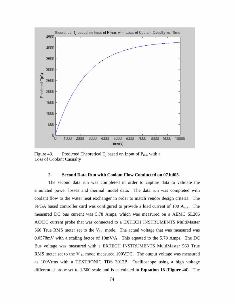
74
Figure 43. Predicted Theoretical Tj based on Input of Pmax with a Loss of Coolant Casualty
2. Second Data Run with Coolant Flow Conducted on 07Jul05. The second data run was completed in order to capture data to validate the
simulated power losses and thermal model data. The data run was completed with
coolant flow to the water heat exchanger in order to match vendor design criteria. The
FPGA based controller card was configured to provide a load current of 100 Arms. The
measured DC bus current was 5.78 Amps, which was measured on a AEMC SL206
AC/DC current probe that was connected to a EXTECH INSTRUMENTS MultiMaster
560 True RMS meter set to the VDC mode. The actual voltage that was measured was
0.0578mV with a scaling factor of 10mV/A. This equated to the 5.78 Amps. The DC
Bus voltage was measured with a EXTECH INSTRUMENTS MultiMaster 560 True
RMS meter set to the VDC mode measured 100VDC. The output voltage was measured
as 100Vrms with a TEXTRONIC TDS 3012B Oscilloscope using a high voltage
differential probe set to 1/500 scale and is calculated in Equation 18 (Figure 44). The

75
Output Current was measured with two TEXTRONIC AS6303 current probes that were
inputted to the two channels of a TEXTRONIC TDS 3012B Oscilloscope and summed
together using the summing function. Two current probes were used because the value of
current was above the rating of each current probe individually. The current was measure
to be 100 Amps seen in Figure 45 and calculated in Equation 19. The ambient room
temperature was recorded to be 25.4°C with a BRAUN SS CO. CAT. No. 610
Laboratory Grade Thermometer. The coolant temperature was recorded to be 21.5°C
with a BRAUN SS CO. CAT. No. 610 Laboratory Grade Thermometer. The flow rate
was calibrated by filling a five gallon bucket four times and averaging the flow rate. The
average was controlled until it was calculated to be 1.40gal/min. This corresponded to a
flow rate of 5.3 l/min, which corresponded to a thermal resistance of 0.018K/W which
was the thermal resistance of the heatsink used for the simulation (Figure 30). This was
done in order to match experimental conditions to previously computer simulated
conditions.
Figure 44. Load Voltage 564mVpp using a High Voltage Differential Probe on Scale 1/500: Therefore showing 100Vrms (Equation 18).
( )LOAD (RMS)
3
rms rms
564*10 500V * =99.7 V 100 V2 2
−⎡ ⎤⎢ ⎥= ≈⎢ ⎥⎣ ⎦
(18)

76
Equation 18. Calculation of Load Voltage for Data Run #2
Figure 45. Load Current for Data Run #2of 56.0mVpp using two current probes and the summing function with 50A/div at the 10mV scale (Equation 19).
( )3
LOAD (RMS)
pp p rms
pp p
56.0 *10 mV 1A 1A50Amps div* * * * = 99.26 A 100 A
rms rmsdiv div 10mV 2A 2A I
−
≈⎡ ⎤
= ⎢ ⎥⎢ ⎥⎣ ⎦
(19)
Equation 19. Calculation of Load Current Voltage for Data Run #2.
The experimental time was measured with a SEIKO ARCTURA stopwatch. The
thermal data that was collected every thirty seconds for until equilibrium was reached
which was 40 minutes. The recorded data is shown in Table 9.
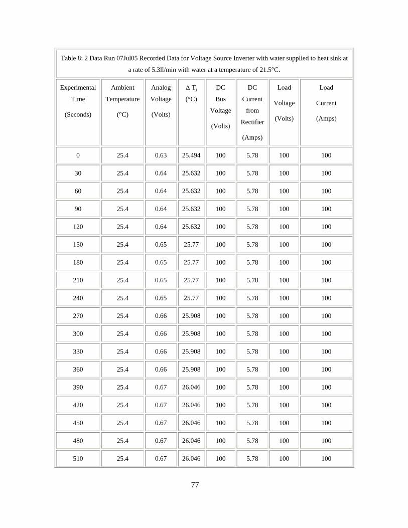
77
Table 8: 2 Data Run 07Jul05 Recorded Data for Voltage Source Inverter with water supplied to heat sink at
a rate of 5.3ll/min with water at a temperature of 21.5°C.
Experimental
Time
(Seconds)
Ambient
Temperature
(°C)
Analog
Voltage
(Volts)
∆ Tj
(°C)
DC
Bus
Voltage
(Volts)
DC
Current
from
Rectifier
(Amps)
Load
Voltage
(Volts)
Load
Current
(Amps)
0 25.4 0.63 25.494 100 5.78 100 100
30 25.4 0.64 25.632 100 5.78 100 100
60 25.4 0.64 25.632 100 5.78 100 100
90 25.4 0.64 25.632 100 5.78 100 100
120 25.4 0.64 25.632 100 5.78 100 100
150 25.4 0.65 25.77 100 5.78 100 100
180 25.4 0.65 25.77 100 5.78 100 100
210 25.4 0.65 25.77 100 5.78 100 100
240 25.4 0.65 25.77 100 5.78 100 100
270 25.4 0.66 25.908 100 5.78 100 100
300 25.4 0.66 25.908 100 5.78 100 100
330 25.4 0.66 25.908 100 5.78 100 100
360 25.4 0.66 25.908 100 5.78 100 100
390 25.4 0.67 26.046 100 5.78 100 100
420 25.4 0.67 26.046 100 5.78 100 100
450 25.4 0.67 26.046 100 5.78 100 100
480 25.4 0.67 26.046 100 5.78 100 100
510 25.4 0.67 26.046 100 5.78 100 100

78
Table 8: 2 Data Run 07Jul05 Recorded Data for Voltage Source Inverter with water supplied to heat sink at
a rate of 5.3ll/min with water at a temperature of 21.5°C.
Experimental
Time
(Seconds)
Ambient
Temperature
(°C)
Analog
Voltage
(Volts)
∆ Tj
(°C)
DC
Bus
Voltage
(Volts)
DC
Current
from
Rectifier
(Amps)
Load
Voltage
(Volts)
Load
Current
(Amps)
540 25.4 0.68 26.184 100 5.78 100 100
570 25.4 0.68 26.184 100 5.78 100 100
600 25.4 0.68 26.184 100 5.78 100 100
630 25.4 0.68 26.184 100 5.78 100 100
660 25.4 0.68 26.184 100 5.78 100 100
690 25.4 0.69 26.322 100 5.78 100 100
720 25.4 0.69 26.322 100 5.78 100 100
750 25.4 0.69 26.322 100 5.78 100 100
780 25.4 0.69 26.322 100 5.78 100 100
810 25.4 0.69 26.322 100 5.78 100 100
840 25.4 0.7 26.46 100 5.78 100 100
870 25.4 0.7 26.46 100 5.78 100 100
900 25.4 0.7 26.46 100 5.78 100 100
930 25.4 0.7 26.46 100 5.78 100 100
960 25.4 0.7 26.46 100 5.78 100 100
990 25.4 0.71 26.598 100 5.78 100 100
1020 25.4 0.71 26.598 100 5.78 100 100
1050 25.4 0.71 26.598 100 5.78 100 100

79
Table 8: 2 Data Run 07Jul05 Recorded Data for Voltage Source Inverter with water supplied to heat sink at
a rate of 5.3ll/min with water at a temperature of 21.5°C.
Experimental
Time
(Seconds)
Ambient
Temperature
(°C)
Analog
Voltage
(Volts)
∆ Tj
(°C)
DC
Bus
Voltage
(Volts)
DC
Current
from
Rectifier
(Amps)
Load
Voltage
(Volts)
Load
Current
(Amps)
1080 25.4 0.71 26.598 100 5.78 100 100
1110 25.4 0.71 26.598 100 5.78 100 100
1140 25.4 0.72 26.736 100 5.78 100 100
1170 25.4 0.72 26.736 100 5.78 100 100
1200 25.4 0.72 26.736 100 5.78 100 100
1230 25.4 0.72 26.736 100 5.78 100 100
1260 25.4 0.72 26.736 100 5.78 100 100
1290 25.4 0.73 26.874 100 5.78 100 100
1320 25.4 0.73 26.874 100 5.78 100 100
1350 25.4 0.73 26.874 100 5.78 100 100
1380 25.4 0.73 26.874 100 5.78 100 100
1410 25.4 0.73 26.874 100 5.78 100 100
1440 25.4 0.73 26.874 100 5.78 100 100
1470 25.4 0.73 26.874 100 5.78 100 100
1500 25.4 0.73 26.874 100 5.78 100 100
1530 25.4 0.74 27.012 100 5.78 100 100
1560 25.4 0.74 27.012 100 5.78 100 100
1590 25.4 0.74 27.012 100 5.78 100 100

80
Table 8: 2 Data Run 07Jul05 Recorded Data for Voltage Source Inverter with water supplied to heat sink at
a rate of 5.3ll/min with water at a temperature of 21.5°C.
Experimental
Time
(Seconds)
Ambient
Temperature
(°C)
Analog
Voltage
(Volts)
∆ Tj
(°C)
DC
Bus
Voltage
(Volts)
DC
Current
from
Rectifier
(Amps)
Load
Voltage
(Volts)
Load
Current
(Amps)
1620 25.4 0.74 27.012 100 5.78 100 100
1650 25.4 0.74 27.012 100 5.78 100 100
1680 25.4 0.74 27.012 100 5.78 100 100
1710 25.4 0.74 27.012 100 5.78 100 100
1740 25.4 0.74 27.012 100 5.78 100 100
1770 25.4 0.74 27.012 100 5.78 100 100
1800 25.4 0.75 27.15 100 5.78 100 100
1830 25.4 0.75 27.15 100 5.78 100 100
1860 25.4 0.75 27.15 100 5.78 100 100
1890 25.4 0.75 27.15 100 5.78 100 100
1920 25.4 0.75 27.15 100 5.78 100 100
1950 25.4 0.75 27.15 100 5.78 100 100
1980 25.4 0.75 27.15 100 5.78 100 100
2010 25.4 0.75 27.15 100 5.78 100 100
2040 25.4 0.75 27.15 100 5.78 100 100
2070 25.4 0.75 27.15 100 5.78 100 100
2100 25.4 0.75 27.15 100 5.78 100 100
2130 25.4 0.75 27.15 100 5.78 100 100
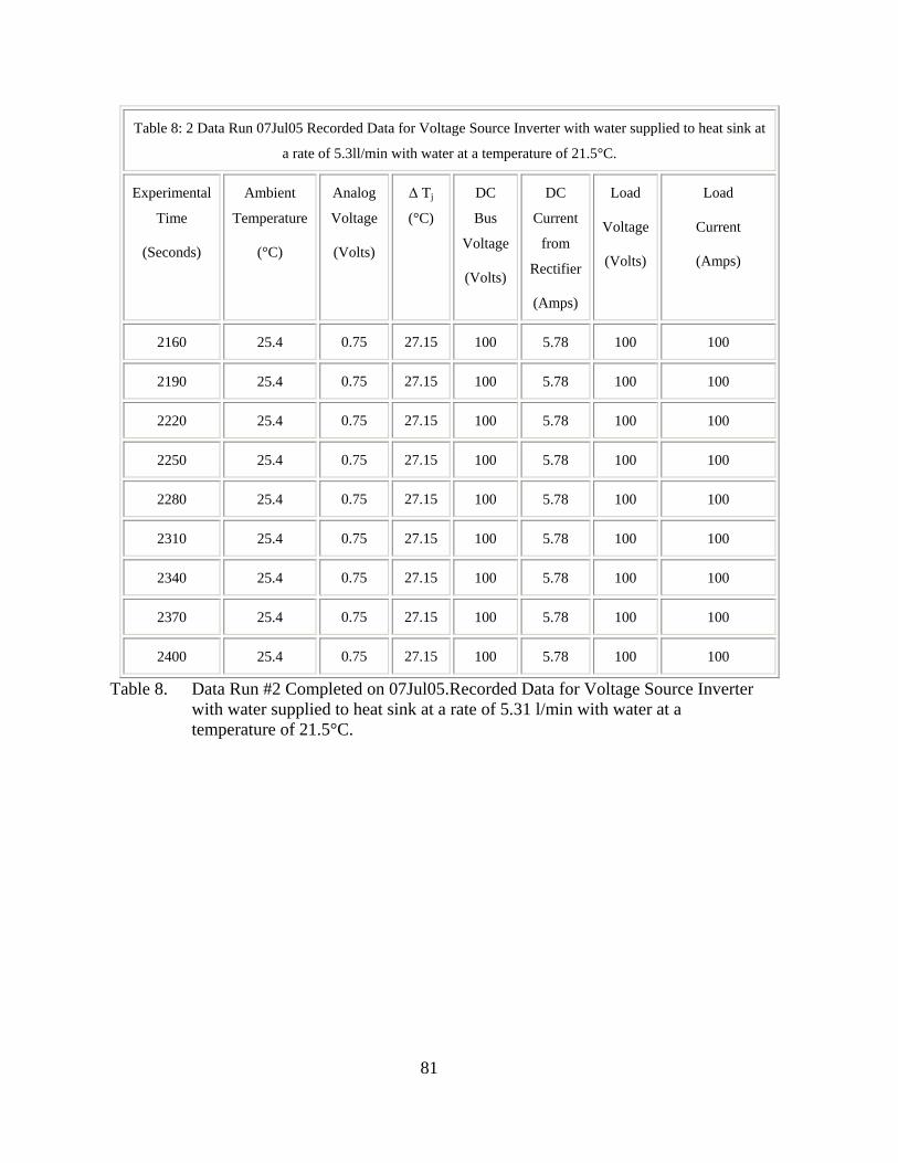
81
Table 8: 2 Data Run 07Jul05 Recorded Data for Voltage Source Inverter with water supplied to heat sink at
a rate of 5.3ll/min with water at a temperature of 21.5°C.
Experimental
Time
(Seconds)
Ambient
Temperature
(°C)
Analog
Voltage
(Volts)
∆ Tj
(°C)
DC
Bus
Voltage
(Volts)
DC
Current
from
Rectifier
(Amps)
Load
Voltage
(Volts)
Load
Current
(Amps)
2160 25.4 0.75 27.15 100 5.78 100 100
2190 25.4 0.75 27.15 100 5.78 100 100
2220 25.4 0.75 27.15 100 5.78 100 100
2250 25.4 0.75 27.15 100 5.78 100 100
2280 25.4 0.75 27.15 100 5.78 100 100
2310 25.4 0.75 27.15 100 5.78 100 100
2340 25.4 0.75 27.15 100 5.78 100 100
2370 25.4 0.75 27.15 100 5.78 100 100
2400 25.4 0.75 27.15 100 5.78 100 100
Table 8. Data Run #2 Completed on 07Jul05.Recorded Data for Voltage Source Inverter with water supplied to heat sink at a rate of 5.31 l/min with water at a temperature of 21.5°C.
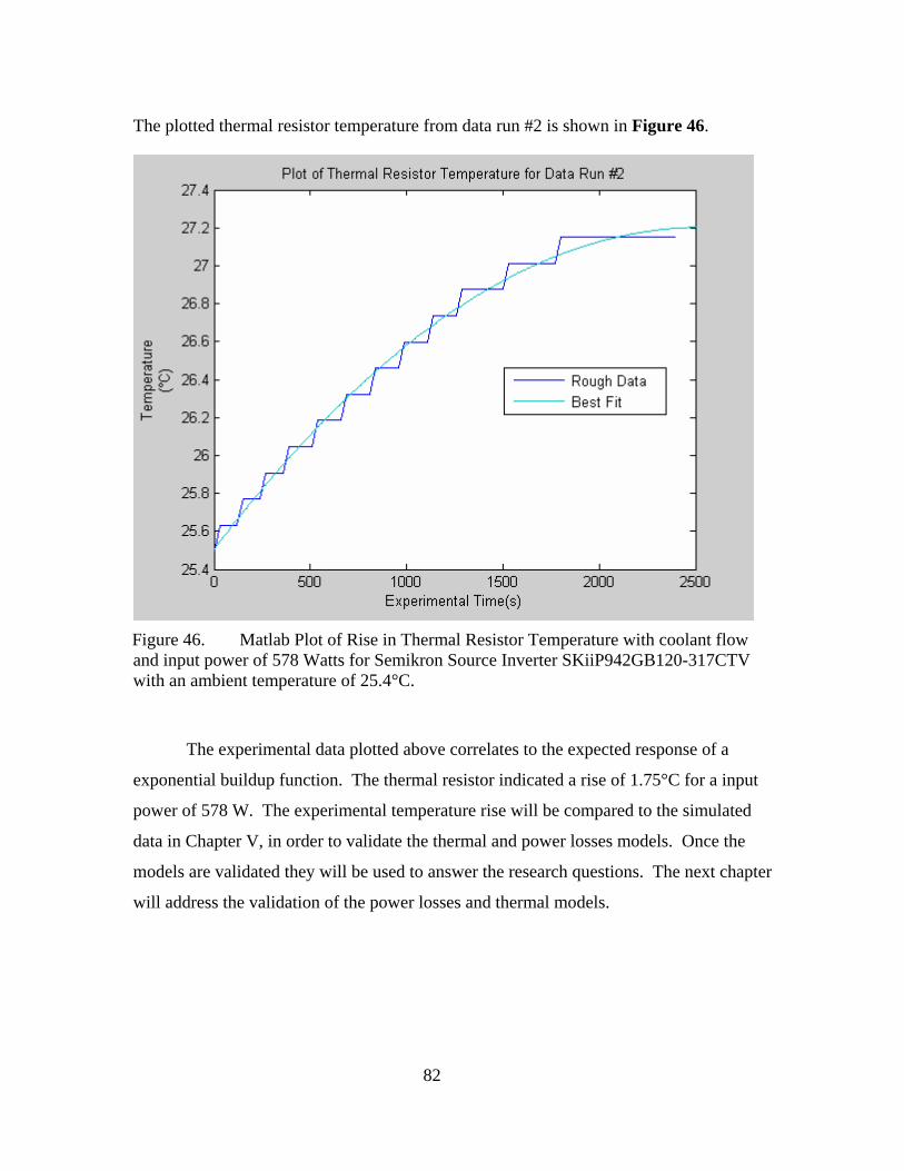
82
The plotted thermal resistor temperature from data run #2 is shown in Figure 46.
Figure 46. Matlab Plot of Rise in Thermal Resistor Temperature with coolant flow and input power of 578 Watts for Semikron Source Inverter SKiiP942GB120-317CTV with an ambient temperature of 25.4°C.
The experimental data plotted above correlates to the expected response of a
exponential buildup function. The thermal resistor indicated a rise of 1.75°C for a input
power of 578 W. The experimental temperature rise will be compared to the simulated
data in Chapter V, in order to validate the thermal and power losses models. Once the
models are validated they will be used to answer the research questions. The next chapter
will address the validation of the power losses and thermal models.

83
D. SUMMARY
The experimental thermal response of the VSI system was a buildup function as
expected. In the plotted thermal data in Figure 46 from data run #2 one can see the
Analog to Digital (A/D) resolution of the A/D converter on the Semikron module as the
temperature steps in incremental amounts. The extrapolated time to shutdown with a
LOCC indicated shutdown in 68.8 seconds. This time is assuming that the system can be
modeled as a first order system. The data was also recorded at a relatively low power
compared to the max design operating power. If the system was operating at the
maximum design power the extrapolated time to shutdown for a LOCC probably would
have been sooner. The lab equipment prevented running the equipment at maximum
design power. The summary of data collected and extracted from data runs 1&2 are
shown in Tables 9&10. In the next Chapter, the experimental data and simulated data
will be compared and the research questions will be addressed.
Data Run #1
Input
Power
Output
Voltage (AC
rms)
Ouput Current
(AC rms)
Temperature Rise/ for Simulation
Time of 7500 seconds
Extracted Max Time
to S/D With a
LOCC
No Coolant 642.6W 100V 100 A 55.2°C 68.8 seconds
Table 9. Summary of Collected and Extracted Data from Data Run #1.
Data Run
#2
Input
Power
Output Voltage (AC
rms)
Output Current (AC
rms)
Temperature Rise/ for Simulation Time of
2400 seconds
Coolant 578 100V 100 A 1.3°C
Table 10. Summary of Collected and Extracted Data from Data Run #2.

84
THIS PAGE INTENTIONALLY LEFT BLANK
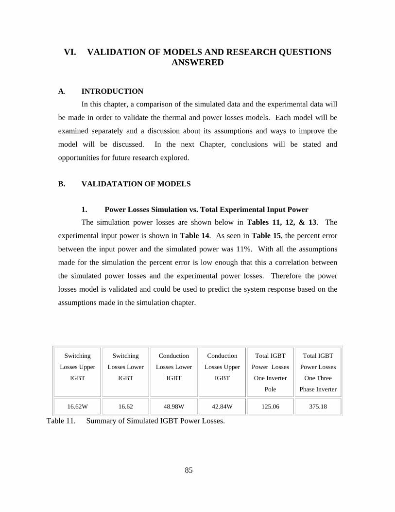
85
VI. VALIDATION OF MODELS AND RESEARCH QUESTIONS ANSWERED
A. INTRODUCTION
In this chapter, a comparison of the simulated data and the experimental data will
be made in order to validate the thermal and power losses models. Each model will be
examined separately and a discussion about its assumptions and ways to improve the
model will be discussed. In the next Chapter, conclusions will be stated and
opportunities for future research explored.
B. VALIDATATION OF MODELS
1. Power Losses Simulation vs. Total Experimental Input Power
The simulation power losses are shown below in Tables 11, 12, & 13. The
experimental input power is shown in Table 14. As seen in Table 15, the percent error
between the input power and the simulated power was 11%. With all the assumptions
made for the simulation the percent error is low enough that this a correlation between
the simulated power losses and the experimental power losses. Therefore the power
losses model is validated and could be used to predict the system response based on the
assumptions made in the simulation chapter.
Switching
Losses Upper
IGBT
Switching
Losses Lower
IGBT
Conduction
Losses Lower
IGBT
Conduction
Losses Upper
IGBT
Total IGBT
Power Losses
One Inverter
Pole
Total IGBT
Power Losses
One Three
Phase Inverter
16.62W 16.62 48.98W 42.84W 125.06 375.18
Table 11. Summary of Simulated IGBT Power Losses.
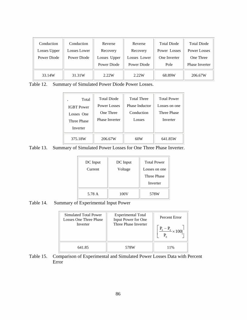
86
Conduction
Losses Upper
Power Diode
Conduction
Losses Lower
Power Diode
Reverse
Recovery
Losses Upper
Power Diode
Reverse
Recovery
Losses Lower
Power Diode
Total Diode
Power Losses
One Inverter
Pole
Total Diode
Power Losses
One Three
Phase Inverter
33.14W 31.31W 2.22W 2.22W 68.89W 206.67W
Table 12. Summary of Simulated Power Diode Power Losses.
. Total
IGBT Power
Losses One
Three Phase
Inverter
Total Diode
Power Losses
One Three
Phase Inverter
Total Three
Phase Inductor
Conduction
Losses
Total Power
Losses on one
Three Phase
Inverter
375.18W 206.67W 60W 641.85W
Table 13. Summary of Simulated Power Losses for One Three Phase Inverter.
DC Input
Current
DC Input
Voltage
Total Power
Losses on one
Three Phase
Inverter
5.78 A 100V 578W
Table 14. Summary of Experimental Input Power
Simulated Total Power Losses One Three Phase
Inverter
Experimental Total Input Power for One Three Phase Inverter
Percent Error
S E
E
P P100
P−
×⎡ ⎤⎢ ⎥⎣ ⎦
641.85 578W 11%
Table 15. Comparison of Experimental and Simulated Power Losses Data with Percent Error

87
2. Thermal Model Simulation Junction Temperatures vs. Experimental IGBT Junction Temperature
The simulated thermal response and experimental thermal response is
summarized in Table 16 from data collected in the simulation and experimental chapters.
As seen in Table 17, the percent error between the simulated thermal response and
experimental thermal response was 28%. The percent error seems higher than expected
but since the change is temperature was small the percent error looks high. If the lab
equipment would support higher currents then the percent error should be lower. With all
the assumptions made for the simulation the percent error is low enough that a correlation
between the simulated thermal response and the experimental thermal response exists.
Therefore the thermal model is validated and could be used to predict the systems thermal
response based on the assumptions made in the simulations chapter.
Table 16. Comparison of Simulated vs. Experimental Thermal Response with Percent Error
C. SIMULATION TO ANSWER RESEARCH QUESTION
1. Simulation to Determine IGBT Junction Temperature at Different Frequencies at Maximum Design Conditions for the 625KW Fuel Cell Reformer Project for ONR
The many simulations were run at different PWM frequencies at the maximum
design operating conditions for the 625KW Fuel Cell Reformer Project for ONR. Some
assumptions were made about worst case conditions for ambient temperature and a
twenty percent tolerance was added to ensure overheating doesn’t occur. The maximum
ambient temperature was chosen to be 40°C which corresponds to 104°F. This
Matlab Simulated
Data (C°)
Lab Experimental
Data
Percent Error
Rise in T(j) (C°)
2.4 1.75 27.4%

88
temperature was based on the worst anticipated ship conditions in the Persian Gulf. The
results of the simulations are shown in Figures 47, 48, and 49. The summary of the
results are shown in Table 17.
Figure 47. Simulated IGBT Junction Temperature from Simulink Thermal Model Using Maximum Design Parameters for the 625Kw Fuel Cell Reformer Project at a PWM switching frequency of 5kHz.

89
Figure 48. Simulated IGBT Junction Temperature from Simulink Thermal Model Using Maximum Design Parameters for the 625Kw Fuel Cell Reformer Project at a PWM Switching frequency of 7 kHz.
Figure 49. Simulated IGBT Junction Temperature from Simulink Thermal Model Using Maximum Design Parameters for the 625Kw Fuel Cell Reformer Project at a PWM switching frequency of 7 kHz.

90
PWM
Switching Frequency
(kHz)
Simulated Hottest
Junction Temperature
(C°)
% Margin to Over
Temperature Protection (110°C)
5 73 34 % 7 86 22%
10 115 Over-Temp Fault
Table 17. Summary of Simulated IGBT Junction Temperature for 625 Fuel Cell Reformer Demonstration for different Frequencies based on Maximum Design Parameters and Maximum Ambient Temperature
The IGBT Junction temperature was the hottest junction temperature at the
maximum design parameters for the 625kW Fuel Cell Reformer Demonstration for ONR.
The maximum design parameters were an input of 350 VDC input with an output of
440VAC at 400 Amps at 60 Hz. The over-temperature protection of the Semikron
module had a temperature range from 110-120 °C. The low range value of 110 was used
and a engineering margin of 20% was added to ensure an over-temperature condition
didn’t exist because of the PWM frequency. The simulated ambient temperature was
increased from the 25.5 °C to 40°C to account for the worst case possible ambient
temperature in a ship environment. As you can see in Table 17, the maximum PWM
switching frequency recommended is 7 kHz which allowed an 20% margin to over
temperature protection set point of 110°C.
D. RESEARCH QUESTIONS READDRESSED In this section all the research questions will be discussed and decided whether
the research goals were met and/or obtained. The goals of this thesis were to model the
power losses for three phase voltage source inverter system using Simulink, model the
thermal response of VSI system using Simulink, build lab system that matches computer
model and collect data in order to validate the computer models, quantify the accuracy of

91
the estimated thermal impedance of an IGBT module, predict the maximum switching
frequency without violating thermal limits for the 625 Fuel Cell Reformer Project of
ONR, predict the time to shutdown on a Loss of Coolant Casualty (LOCC), and quantify
the characteristics of the heat-sink needed to dissipate the heat under worst case
conditions.
The simulated power losses of the three phase VSI inverter had an accuracy of 11
% (Table 15) compared to the experimental data. This shows that by taking the vendor
data one can accurately create a power losses model of a half bridge VSI by counting
switching events of the four semiconductor devices and determining when each one is
conducting. Although the experimental data was taken at low power due to insufficient
lab equipment one could expect the same or a better response at higher power.
The simulated delta thermal response of the IGBT Junction temperature of a half-
bridge VSI inverter had an percent error of 27 % (Table 16). Although, the percent error
seems high at the low power the experiment was conducted at the percent error should
decrease when run at a higher power because the change in temperature will be larger and
the difference smaller. A thermal model of a half bridge VSI can be created by taking the
vendor data and creating a model of the system. The cost of design and production of
half-bridge IGBT VSI’s can be reduced if one takes the time to create and validate a
power losses and thermal models. These tools can allow designers and manufactures to
create a product that will work and won’t have to create many different prototypes to
achieve the desired results.
The predicted time to shutdown on a LOCC was 68.8 seconds for the 625kW
Fuel Cell Reformer project. The maximum PWM switching frequency for the 625kW
Fuel Cell Reformer project is 7 kHz which allowed an 20% margin to over temperature
protection set point of 110°C.

92
THIS PAGE INTENTIONALLY LEFT BLANK

93
VII. CONCLUSIONS
A. CHAPTER OVERVIEW This chapter summarizes the research performed in this thesis and discusses the
results of Thermal and Power Loss Models of a Voltage Source Inverter. Also, possible
areas for future research are also discussed.
B. SUMMARY The goal of this thesis was to show that one can take the vendor data for a voltage
source inverter given a valid electrical model and accurately simulate a power loss and
thermal model and that these models would allow one to reduce the cost of design and
production, increase reliability, quantify the accuracy of the estimated thermal impedance
of an IGBT module, predict the maximum switching frequency without violating thermal
limits and to quantify the characteristics of the heat-sink needed to dissipate the heat
under worst case conditions. This thesis particularly was focused on a voltage source
inverter used in the development of a 625KW Fuel Cell and Reformer demonstration for
ONR (Office of Naval Research).
The power losses model of the Semikron VSI module was initially created in
Simulink with input variables set to an obtainable lab conditions so that experimental
data could be collected. The thermal model was defined and then created in Simulink
and calibrated to the Semikron VSI Module and heatsink with an input that was the
average power output of the semiconductor devices of the power losses model. The
power losses model was then simulated and data collected. The thermal model was then
simulated with the average power outputs of the semiconductor devices from the power
losses model simulation. The experimental lab conditions were set up to match the
models simulated conditions. Two data runs were performed, one without coolant in
order to calculated the time to shutdown on over-temperature protection on a LOCC. The
second experimental data run with coolant flow was to collect experimental data to
compare to the simulated models in order to validate them. The data was compared and it
was determined that a strong correlation was present between the experimental data and

94
the simulated data. The power losses and thermal simulation were then run many times to
determine the maximum PWM switching frequency for the 625 Kw Fuel Cell Reformer
Project of ONR.
C. CONCLUSIONS This thesis indicates one can take the vendor data for a VSI given a valid
electrical model and accurately simulate power loss and thermal models. Once created
the validated models will allow engineers to reduce the cost of design and production,
increase reliability, quantify the accuracy of the estimated thermal impedance of an IGBT
module, predict the maximum switching frequency without violating thermal limits, and
to quantify the characteristics of the heat-sink needed to dissipate the heat under worst
case conditions. The summary of the results of this thesis are shown in Table 18.
Matlab Simulated
Data
Lab Experimental
Data
Percent Error
Rise in ∆T(j) (C°) 2.4 1.75 27.4%
Power Losses (W) 636.7 578 9%
Extrapolated Time to
Shutdown on LOCC
(seconds)
68 NA NA
Maximum PWM Switching Frequency
(kHz)
7 NA NA
Table 18. Summary of Thesis Results and Goals
D. FUTURE WORK There are several opportunities for future work in this area. Additional
investigation would be best suited to try collecting experimental and simulated data at the
maximum design ratings of the 625KW fuel cell reformer project. The correlation

95
between simulated data and the data collected at the maximum design ratings should be
higher. Currently, the lack of adequate lab equipment and power precludes this from
happening. Another area for future research would be the method of switching could be
varied to see which method of switching (PWM, space vector, hysteresis, etc) gives the
best quality power with the least amount of heat generated.

96
THIS PAGE INTENTIONALLY LEFT BLANK

97
APPENDIX A

98
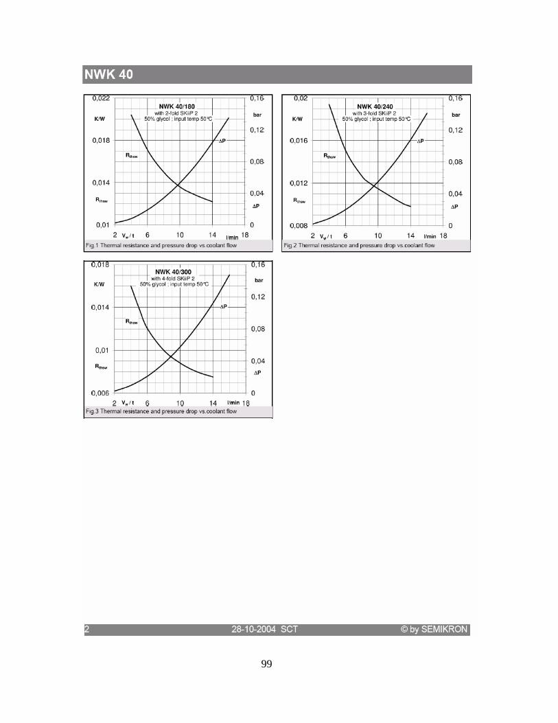
99

100
THIS PAGE INTENTIONALLY LEFT BLANK

101
APPENDIX B
A. MATLAB M-FILE FOR POWER LOSSES MODEL
Filename: fuel_cell_intlab5.m
i_load=100; %Sets load current% ffilter=4000; Tsw = (2*100*10^-6); %PWM switching frequency f_fund = 60; %Fundamental output frequency% Vdc=100; %Input Voltage to inverters omega=2*pi*60; oversample=1; tstep = Tsw/100; %sets step size% tstop=20/f_fund %sets simulation stop time% Lfa=90*10^-6; Lfb=Lfa; Lfc=Lfa; Cf= (170+6*45)*1e-6*3; Cfa=Cf; Cfb=Cfa; Cfc=Cfb; alpha=0*2*0.2*sqrt(Lfa*Cfa)/Vdc;%active damping gain Loa=900*10^-6; Lob=Loa; Loc=Loa; Roa=0.023; %current is in phase winding, system is characterized for a delta connected winding Rob=Roa; Roc=Roa; %Kp_i=sqrt(3)/Vdc/8; %Ki_i=1000*sqrt(3)/Vdc/8; %Current control loop gain Kp_i=.01;%current PI gain is amplified to account for the SV modulation scaling Ki_i=.5; %Current control loop gain %Kp_v=.2; Kp_v=.5; Kp_rms=0; Ki_rms=0; %Voltage control loop gain %Kp_i=.0005/2; %Ki_i=10/4; %Kp_v=.00005*200; %Ki_v=20*4; Amat_indI = zeros(2); Bmat_indI = inv([Lfa -Lfb;Lfc Lfb+Lfc]); Cmat_indI = [1 0 ;0 1 ;-1 -1 ]; %Ic = -Ia-Ib Dmat_indI = zeros(3,2);
102
Filename: fuel_cell_intlab5.m(continued) Amat_caps = zeros(3); Bmat_caps = [1/Cfa 0 0; 0 1/Cfb 0; 0 0 1/Cfc]; Cmat_caps = eye(3); Dmat_caps = zeros(3); Amat_load = [-Roa/Loa 0 0; 0 -Rob/Lob 0; 0 0 -Roc/Loc]; Bmat_load = [1/Loa 0 0; 0 1/Lob 0 ; 0 0 1/Loc]; Cmat_load = eye(3); Dmat_load = zeros(3); one_zero_state=0; %Set to one so that only one zero state is used in modulation if one_zero_state == 1 gain1 = 1; gain2 = 0; else gain1 = 1/2; gain2 = 1; end turns_ratio=208/480/sqrt(3); trans1=turns_ratio*sqrt(3)/2*[sqrt(3) 1 0;-1 sqrt(3) 0;0 0 0]; trans1_qd=trans1(1:2,1:2); trans2=turns_ratio*sqrt(3)/2*[sqrt(3) -1 0;1 sqrt(3) 0;0 0 0]; trans2_qd=trans2(1:2,1:2); trans3=1/(turns_ratio*sqrt(3)/2)*[sqrt(3)/4 1/4 0;-1/4 sqrt(3)/4 0; 0 0 0];

103
LIST OF REFERENCES
[1] William F. Weldon, et al. “Roadmap to an Electric Naval Force,” NRAC Report 02-01, NRAC, Arlington, VA, March 2003
[2] Brad P. Bittle, “Hysteresis Control of Parallel Connected Hybrid Inverters”,
Masters Thesis, Naval Post Graduate School, Monterey California, September 2005. [3] Mike Collins, “DD(X) IPS Revolution in Shipboard Power,” NAVSEA
PEO-510 Internal Presentation, Washington D.C., February 2003 [4] R. Steck, et al. “Surface Ship Thermal Management Survery-Part 1,”
CARDIVNSWC-TR-92-03-21, CARDDIVNSWC, Philadelphia, PA, July 2003 [5] IEEE Power Electronics Subcommittee Task Force 2, “Power Electronics
Building Block Concepts,” IEEE Power Engineering Society Report 04TP170, IEEE Press, New York, 2004
[6] “Semikron Application Notes for Skiip Modules” Semikron website,
www.semikron.com, last accessed 19 January 2006
[7] A. Bruce Carlson, “CIricuits” pp (254-258), Brooks/Cole Thomson Learning, Inc., 511 Forest Lodge Rd. Pacific Grove, California, 2000
[8] Ned Mohan, Tore M Undeland, and William P Robbins, “Power
Electronics, 3rd Edition,” pp (225-248), John Wiley and Sons, Inc., Hoboken, New Jersey, 2003
[9]Vladimir Blasko, Rich Lukaszewski, and Ray Sladky, “Online Thermal Management Strategy of a Three Phase Voltage Source Inverter”, Proc. IEEE Industry Applications Society 34th Annual Meeting, pp. 1423-1431, 1999.
[10] Zhaohui Luo, Hyungkeun Ahn and Mahnoud A El Nokali, “A Thermal Model for Insulated Gate Bipolar Transistor Module”, Proc. IEEE Transactions on Power Electronics VOL. 19. No. 4., pp. 902-907, July 2004.
[11]H. Alan Mantooth and Allen R. Hefner. Jr. “ Electo-thermal Simulation of an IGBT PWM Inverter”, National Institute of Standards and Technology, pp. 77-84, 1993.
[12] Zhaohui Luo, Hyungkeun Ahn and Mahnoud A El Nokali, “A Thermal
Model for Insulated Gate Bipolar Transistor Module”, Proc. IEEE Transactions on Power Electronics VOL. 19. No. 4., pp. 902-907, July 2004.
104
[13] L. W. Nagel, “SPICE2: A computer Program to simulate semiconductor circuits”, ERL Memo. ERL-M-520, University of California, Berkley, 1975.
[14] G. N. Ellision, “Thermal Computations for Electronic Equipment”, Van
Nostrand Reinhold: New York, 1984. [15] A. R. Hefner, “Semiconductor Measurement Technology: INTANT-IGBT
Network Simulation and Transient Analysis Tool”, NIST Special Publication 400-88, 1992.
[16] A. R. Hefner and D. M. Diebolt, “An Experimentally Verified IGBT Model Implemented in the Saber Circuit Simulator,” IEEE PESC Conf. Rec., 1991.
[17] A. R. Hefner and D. L. Blackburn, “Simulating the Dynamic Electro-
Thermal Behavior of Power Electronics Circuits and Systems,” Conf, Rec. IEEE Workshop on Computers in Power Electronics, 1992.
[18] A. R. Hefner, “A Dynamic Electro-Thermal Model for the IGBT,” IEEE IAS
Conf. Rec., 1992. [19] A. R. Hefner and D. L. Blackburn, “Thermal Component Models for Electro-
Thermal Network Simulation,” Proc. IEEE Semiconductor Thermal Measurement and Management SEMI-THERM Symposium, 1993.
[20] Brian E. Souhan, “Closed Loop Control of Cascaded Multi-level Converter
to minimize Harmonic Distortion”, Masters Thesis, Naval Post Graduate School, Monterey California, June 2005.
105
INITIAL DISTRIBUTION LIST
1. Defense Technical Information Center Ft. Belvoir, VA
2. Dudley Knox Library Naval Postgraduate School Monterey, CA
3. Naval Surface Warfare Center Carderock Division Code 984 Attn: Tom Fikse Philadelphia, PA
4. Office of Naval Research Code 334, Room 669 Attn: Terry Ericksen Arlington, VA
5. Dr. Jeffrey Knorr, Chairman, Department of Electrical and Computer Engineering Code EC/Ko Naval Postgraduate School Monterey, CA
6. Dr. Robert W. Ashton, Department of Electrical and Computer Engineering Code EC/Ah Naval Postgraduate School Monterey, CA
7. Dr. Alexander Julian, Department of Electrical and Computer Engineering Code EC/Jl Naval Postgraduate School Monterey, CA