Embed Size (px)
Citation preview
AD-A238 596IlJ 1111 ll 1 11111 111! 1111 1( lii 11111
NAVAL POSTGRADUATE SCHOOLMonterey, California
THESIS
DESIGN OF A STABILIZED, DC-POWEREDANALOG LASER DIODE DRIVER
by
John Joseph Bradunas
September 1990
Thesis Advisor: John P. Powers
Approved for public release; distribution is unlimited
91-04991

BestAvai~lable
Copy

UNCLASSI FIEDSECURITY CLASSIFICATION OF THIS PAGE
Form ApprovedREPORT DOCUMENTATION PAGE OMB No 0704-0188
la REPORT SECURITY CLASSIFICATION lb RESTRICTIVE MARKINGSUNCLASSIFIED2a SECURITY CLASSIFICATION AUTHORITY 3 DISTRIBUTION, AVAILAB!LITY OF REPORT
Approved for public release;2b DECLASSIFICATION/ DOWNGRADING SCHEDULE distribution is unlimited
4 PERFORMING OR%3ANIZATION REPORT NUMBER(S) 5 MONITORING ORGANIZATION REPORT NUMBER(S)
6a NAME OF PERFORMING ORGANIZATION 6b OFFICE SYMBOL 7a NAME OF MONfiORING ORGANIZATION(If applicable)
Naval Postgraduate School EC Naval Postgraduate School6c. ADDRESS (City, State, and ZIP Code) 7b ADDRESS (City, State, and ZIP Code)
8a. NAME OF FUNDING SPONSORING 8b OFFICE SYMBOL 9 PROCUREMENT INSTRUMENT IDENTIFICATION NUMBERORGANIZATION (If applicable)
8c. ADDRESS (City, State, and ZIP Code) 10 SOURCE OF FUNDING NUMBERSPROGRAM PROJECT TASK WORK UNITELEMENT NO NO NO jACCESSION NO
11 TITLE (Include Security Classification)DESIGN OF A STABILIZED, DC-POWERED LASER DIODE DRIVER
12 PERSONAL AUTHOR(S)
BRADUNAS, John J.13a TYPE OF REPORT 13b TIME COVERED 14 DATE OF REPORT (Year.MonthDay) 15 PAGE COUNT
Master's Thesis FROM _ TO September 199016 SUPPLEMENTARY NOTATION The views expressed in this thesis are those of theauthor and do not reflect the official policy or position of the Depart-ment of Defense or the US Government.
17 COSATI CODES 18 SUBJECT TERMS (Continue on reverse if necessary and identify by block number)
FIELD GROUP SUB-GROUP semiconductor laser diode; thermoelectriccooling; laser diode driver; intensitymodulation
19 ABSTRACT (Continue on reverse if necessary and identify by block number)This thesis presents the design, implementation and evaluation of a de-powered, stabilized-output laser diode drive unit for use in an analogfiber-optic communication transmitter. The driver circuits provide fora stable temperature-controlled operating environment by monitoring thethermistor in the laser diode module and by controlling the current tothe module's integral thermoelectric cooler. Output optical power ismaintained at desired bias and peak-to-peak levels by processing thesignal from the monitor photodiode and amplifying (if necessary) the acand dc drive units. These efforts offset the degradation of the laserdiode's capabilities due to heat and age.
20 DISTRIBUTION, AVAILABILITY OF ABSTRACT 21 ABSTRACT SECURITY CLASSIFICATION
JOUNCLASSIFIED/UNLIMITED 0J SAME AS RPT 0] DTIC USERS UNCLASSIFIED22a NAME OF RESPONSIBLE INDIVIDUAL 22b TELEPHONE (Include Area Code) 22c OFFICE SYMBOL
POWERS, John P. 408-646-2679 EC/Po
DD Form 1473, JUN 86 Previous editions are obsolete SECURTY CLASSIFICATION OF I-IS PAGE
S/N 0102-LF-014-6603 UNCLASSIFIEDi

Approved for public release; distribution is unlimited.
Design of a Stabilized, DC-Powered
Analog Laser Diode Driver
by
John J. BradunasMajor, United States Marine Corps
B.S., Cornell University
Submitted i!-, partial fulfillmentof the requirements for the degree of
MASTER OF SCIENCE IN ELECTRICAL ENGINEERING
from the
NAVAL POSTGRADUATE SCHOOL
September 1990
Author: ___
U-'-Aohn J. Bradunas
Approved by:
John P. Powers, Thesis Advisor
Sherif Michael, Second Reader
Michael A. Morgan, ChairmanDepartment of Electrical and Computer Engineering
ii

ABSTRACT
This thesis presents the design, implementation and evaluation of a dc-
powered, stabilized-output laser diode drive unit for use in an analog fiber-optic
communication transmitter. Th-_ 'river circuits provide for a stable temperature-
controlled operating environment by monitoring the thermistor in the laser diode
module and by controlling the current to the module's integral thermoelectric
cooler. Output optical power is maintained at desired bias and peak-to-peak
levels by processing the signal from the laser diode's monitor photodiode and
amplifying (if necessary) the ac and dc drive currents. These efforts offset the
degradation of the laser diode's capabilities due to heat and age.
*coesslon For
NTTS GRA&IDTIC TAB
....... By .ll P " _Dist r',t'ut Iou/
Availability Codes
_ .... .: an c . .Dist Spooial

TABLE OF CONTENTS
I. INTRODUCTION ................................... 1
A. BACKGROUND ............................... 1
B. THESIS OBJECTIVES ........................... 1
C. SYSTEM DESIGN OVERVIEW ........................ 3
II. LASER DIODE PHYSICS ............................ 5
A. RADIATIVE RECOMBINATION ........................ 5
B. LASING CAVITIES ............................. 8
C. OUTPUT CHARACTERISTICS ..................... 10
D. LASER DIODE MATERIALS ...................... 11
E. LASER DIODE DESIGNS ........................ 13
1. Single Heterostructures ........................ 13
2. Double Heterostructures ....................... 14
F. RELIABILITY ................................ 21
G. CHOICE OF SOURCE ........................... 22
H. SUM MARY .................................. 25
III. TEMPERATURE STABILIZATION NETIWORK ............... 27
A. THERMOELECTRIC COOLING .................... 27
iv

1. Peltier Effect .................................. 27
2. Design Parameters ............................. 29
3. R eliability ................................. 32
4. TEC Limitations ............................... 32
B. CIRCUIT IMPLEMENTATION ....................... 33
1. System Design .............................. 33
2. Wiper Voltage versus Temperature Relationship ........ ,U
3. System Flexibility ............................ 44
C. SUM M ARY .................................. 44
IV. POWER STABILIZATION NETWORK ..................... 45
A. REQUIREMENTS FOR STABILIZATION .............. 45
B. PHOTODIODE CURRENT-TO-VOLTAGE CONVERTER ... 48
1. Photodiode Operation ............................ 48
2. Transimpedance Amplifier .. ...................... 49
C. DRIVE CURRENT COMPENSATION CIRCUITRY ........ 51
1. Output Bias Sensor .. .......................... 51
2. Signal Peak-to-Peak Sensor .. ..................... 51
3. Bias Compensation Circuit ........................ 57
4. Automatic Gain Control Circuit . .................. 61
5. Final Summing Circuit .. ........................ 64
D. DRIVE "CURRENT' LIMITER ....................... 65
E. SURGE PROTECTION ............................ 68
v

F. VOLTAGE-TO-CURRENT CONVERTER CIRCUIT ........ 69
G. SUM M ARY .................................. 71
V. TEST AND EVALUATION ............................. 72
A. INTRODUCTION ................................. 72
B. EVALUATION PROCEDURE ........................ 72
1. Test Equipment and Set-up .. ..................... 72
2. Operating Procedures ... ........................ 73
a. Start-up .. ............................... 73
b. Laser Diode Modulation ...................... 75
c. Shut-down ... ............................. 75
C. DRIVING THE LASER DIODE WITH DC SIGNALS ..... 76
1. Without Temperature Stabilization ................... 76
2. With Temperature Stabilization ..................... 83
D. MODULATING THE LASER DIODE ................. 89
1. Veiifying Network Design .. ...................... 89
2. Too Little/Too Much Output Bias .. ................ 93
3. Minimum/Maximum Modulation Limits .............. 95
4. Dynamic Range ............................. 97
E. SUM MARY .................................. 99
VI. CONCLUSIONS ................................... 101
A. SUMMARY OF RESULTS ........................ 101
vi

Et. AREAS FOR FURTHER STUDY...................... 101
LIST OF REFERENCES.................................... 103
INITIAL DISTRIBUTION LIST............................... 106
vii

LIST OF TABLES
1. QLM-1300-SM-BH LASER DIODE ....................... 25
2. WIPER VOLTAGE VERSUS THERMISTOR RESISTANCE ...... 40
3. RESPONSE WITHOUT TEMPERATURE STABILIZATION ...... 77
4. DESIRED VERSUS ACTUAL OPTICAL OUTPUT BIAS LEVELS 82
5. TEMPERATURE STABILIZATION TEST VALUES ............. 84
6. TEMPERATURE-STABILIZED LASERTRON RESPONSE ....... 85
7. TEMPERATURE DEPENDENCE OF PHOTODIODE CURRENT 86
8. DESIRED VERSUS ACTUAL OUTPUT POWER FLUCTUATION 90
9. GAIN-PHASE RESPONSE OF STABILIZATION NETWORK ...... 98
viii

LIST OF FIGURES
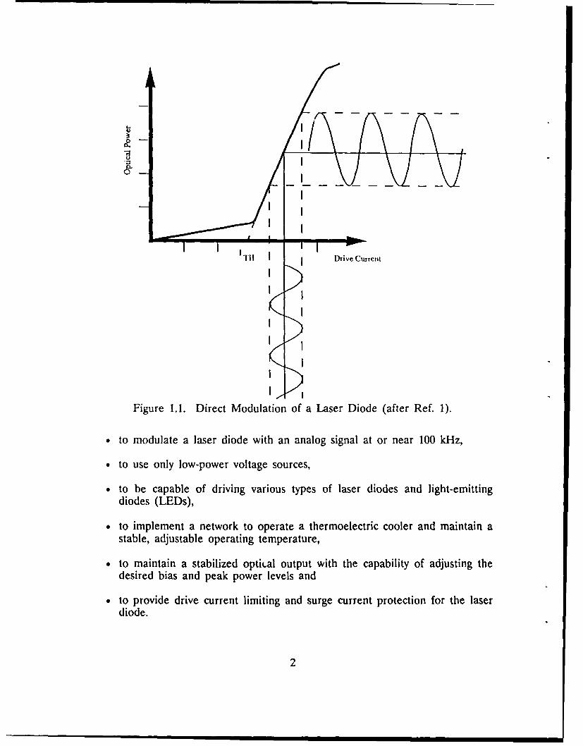
1.1. Direct Modulation of a Laser Diode ..................... 2
1.2. Functional Schematic of a Laser Transmitter ................... 4
2.1. Energy Level Diagram of a pn-junction ........................ 7
2.2. Transfer Function of a Laser Diode ...................... 9
2.3. Temperature Dependence of a Laser Diode ................... 12
2.4. Double Heterostructure Laser Diode ........................ 15
2.5. Energy Level Diagram of a Double Heterostructure Laser Diode . 17
2.6. End View of a Buried Heterostructure InGaAsP/InP Laser Diode . 19
3.1. Thermoelectric Cooling Couple ......................... 28
3.2. Feedback Loop for Temperature Control ..................... 33
3.3. Thermistor Temperature versus Resistance .................... 34
3.4. Voltage Regulators ................................. 36
3.5. Precision +2 V DC Regulator ......................... 37
3.6. TEC Drive Circuit ................................. 38
3.7. Thermistor Temperature versus R10 Wiper Voltage ............. 41
3.8. Set-point Temperature versus Wiper Voltage ................... 43
4.1. Effect of Aging and Heat on Optical Output ................... 45
4.2. Power Stabilization Network ........................... 47
4.3. Photodiode Current versus Optical Power .................. 49
ix

4.4. Transimpedance Amplifier ............................ 50
4.5. Photodiode Output Analyzer ........................... 52
4.6. Properly Clamped Signal ............................. 53
4.7. Signal Clamped Above Ground ......................... 54
4.8. Signal Clamped Below Ground ......................... 55
4.9. Bias Compensation Circuit ............................ 58
4.10. Automatic Gain Control Circuit ........................ 62
4.11. Final Summing Circuit .............................. 64
4.12. Drive "Current" Limiter .................................. 66
4.13. Clipped Signal ......................................... 67
4.14. "Slow-on Slow-off' Power Supply ........................... 68
4.15. "Slow-on Slow-off' Circuit ............................ 69
4.16. Voltage Controlled Current Source ...................... 70
5.1. Test Equipment Set-up .............................. 73
5.2. Optical Output versus Drive Current (Not Temperature Stabilized) 78
5.3. Optical Output versus Photodiode Current (Not Temperature Stabilized)80
5.4. Thermistor Resistance versus Output Power ..................... 81
5.5. Module Temperature versus Output Power .................... 81
5.6. Optical Output versus Drive Current (Temperature Stabilized) . . .. 87
5.7. Optical Output versus Photodiode Current (Temperature Stabilized) . 88
5.8. Modulated Laser Diode Current ............................ 89
5.9. Modulated Triangular Wave ................................ 92
5.10. Modulated Square Wave ................................. 92
x

5.11. Current-limited W aveform ................. .......... 93
5.12. Modulation with Too Little Bias ....................... 94
5.13. Modulation with Too Much Bias ....................... 95
5.14. Minimum Detectable Modulation ....................... 96
5.15. Maximum Allowable Modulation ....................... 96
5.16. Dynamic Range of Stabilization Networks ................. 100
xi

I. INTRODUCTION
A. BACKGROUND
This thesis is a continuation of ongoing research being conducted at the
Naval Postgraduate School involving the development of fiber-optic communication
links for use in hostile environments. The particular goal of this research effort
was to design, implement and evaluate a stabilized, dc-powered laser diode (LD)
drive unit which can be used to transmit analog signals over fiber-optic cables.
The light output of a laser diode can be directly modulated by varying the
amount of applied current. The results of this method can be seen in the typical
output versus drive current curve shown in Fig. 1.1. Such a modulation technique
has the advantage of simplicity and the potential for high-speed operation.
However, the physical process of producing coherent light creates thermal and
aging problems which directly affect the operational stability of the laser diode,
possibly resulting in an undesirable optical output or even damage to the module
itself. Consequently, a network was created which maintains a stable operating
environment within the module and which can electrically modify the input to the
laser diode in order to achieve desired optical levels.
B. THESIS OBJECTIVES
The major design requirements for the driver mechanism built during this
thesis effort were:
0
!"i'l I I Drive Curem
Figure 1.1. Direct Modulation of a Laser Diode (after Ref. 1).
" to modulate a laser diode with an analog signal at or near 100 kHz,
* to use only low-power voltage sources,
" to be capable of driving various types of laser diodes and light-emittingdiodes (LEDs),
* to implement a network to operate a thermoelectric cooler and maintain astable, adjustable operating temperature,
* to maintain a stabilized optiial output with the capability of adjusting thedesired bias and peak power levels and
* to provide drive current limiting and surge current protection for the laserdiode.
2

C. SYSTEM DESIGN OVERVIEW
Figure 1.2 is a simplified functional schematic of a laser transmitter. Those
items enclosed by the dashed lines are normally included in a single laser diode
module. The two major components of the stabilization mechanism, the cooling
system and bias network, are discussed in detail in this thesis. Chapter II
discusses the operation of a laser diode, highlighting the specific problems which
affected the network design. Chapter III describes the temperature stabilization
circuit, specifically addressing the Peltier effect and the technique of thermoelectric
cooling. Chapter IV presents the network used to maintain the bias point and the
peak optical output power levels from the laser diode; this involves the extensive
use of high-speed operational amplifiers (op-amps) in signal-processing circuits.
Both stabilization networks are tested and evaluated in Chapter V by using the
driver to transmit various waveforms via a fiber optic cable. Finally, Chapter VI
contains concluding remarks and recommendations for areas of further research.
3

0
CAi

II. LASER DIODE PHYSICS
A. RADIATIVE RECOMBINATION
Energy level diagrams for semiconductor materials used in lasing are not as
sharp and distinct as those of other lasing media such as ruby or neon. Atoms
in n- and p-type materials are packed so closely together that separate energy
levels are difficult to distinguish; therefore the levels are grouped into bands.
Although energy distributions within the semiconductors can still be represented
by the Einstein relations for absorption and emission, optical transitions are
between bands vice discrete energy levels.
Electrons with the highest energy (i.e., those in the outermost ring around
their nucleus) occupy the conduction band. These electrns have enough energy
to carry an electrical current and consequently move easily through the
semiconductor material. The next highest energy state is the valence band; at
these levels, electrons are still tied to their parent nucleus and cannot carry a
current, however they can be excited and moved to the conduction band. In order
for an electron to transition to the higher band, it must receive sufficient energy
to exceed the gap potential between the valence and conduction bands. In
addition to the absorption of this energy difference, the probability of such a
transition must also be sufficiently high. If both of these conditions are met, the
basic building blocks for the creation of light exist, an excited electron in a high-
energy band and a matching positive carrier (i.e., hole) ready for recombination.
5

At the junction of an n- and p-type semiconductor, a thin depletion region
is formed by the recombination of these carriers. As shown in Fig. 2.1a, this
region forms a barrier (or bandgap) potential between the n- and p-type materials.
With no voltage applied across the semiconductor, the barrier prevents the
interdiffusion of charge carriers (the holes and electrons) from their respective
regions. When a forward voltage is applied as in Fig. 2.1b, the barrier is reduced
and carriers are "injected" into the junction region--hence, the term injection laser
[Ref. l:p. 12].
Equilibrium is achieved via two types of recombination. Nonradiative
recombinations result in vibrations in the materials crystal lattice, producing heat
[Ref. 2:p. 249]. However, if the recombination is radiative, a photon is emitted;
the amount of energy in the released photon approximately equals E., the
bandgap potential between the valence and conduction bands of the material. The
wavelength of the light emitted is determined by
U. _(2.1)E9
where h is Planck's constant (6.63 x 10⁻³⁴ J-s) and c is the speed of light in a
vacuum (3.00 x 10⁸ m-s-). This phenomenon of light production via induced
carrier recombination at the junction of semiconductor material is called
"electroluminescence." [Ref. 1:p. 11]
Up to this point, discussion of the production of light has not distinguished
between the types of emissions that could result from radiative recombinations.
As noted, the application of a forward voltage across a semiconductor, inducing
6

CONDUCTION BAND
T BANDGAP
Barrier
e-j { e Holes
IeeeeIJunction
I I
VALENCE BAND
a) No Voltage Applied
CONDUCTION BAND
Barrier Electrons
Barrierhv
[ Holes
I IJunction
VALENCE BAND
b) Forward Voltage Applied
Figure 2.1. Energy Level Diagram of a pn-Junction (after Ref. 1).
7

a current through the structure, can lead to the release of photons. If this current
is kept below a certain critical value, called the lasing threshold (or ITH) , the
semiconductor device emits noncoherent light spontaneously and randomly (i.e.,
it functions as a light emitting diode). However, when sufficient current is applied
to the junction, more electrons are moved to an excited state and a population
inversion is achieved. At that time a randomly emitted photon from a
recombination can act to stimulate another recombination and emission, which can
emit another photon, and so on. This chain reaction amplifies the light as it
passes through the material, producing a coherent output (hence the acronym
LASER--Light Amplification by Stimulated Emission ot Radiation).
Semiconductor devices which can act as lasers are known as semiconductor laser
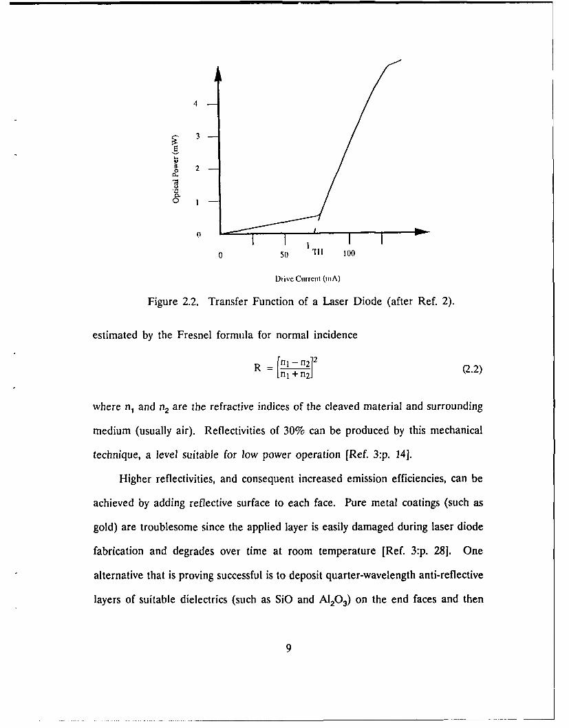
diodes, or simply laser diodes. Figure 2.2 shows a typical power versus current
relationship in a laser diode; the effect of a drive current exceeding ITH is
apparent by the increased slope of the output curve.
B. LASING CAVITIES
In order to sustain this amplification, opposite faces of the semiconductor
structure are cleaved along crystalline planes to create parallel reflective surfaces.
This in effect forms an optical cavity similar to a Fabry-Perot interferometer.
The end mirrors created by the cleaving reflect some of the photons back into the
active light-producing region surrounding the pn-junction. The feedback creates
an oscillatory wave of light along the junction which equals cavity losses and helps
to sustain the stimulated emissions. The reflectivity at the cleaved surface can be
8
4
E3
0 2
S5o T1I 100
Drive Current (mA)
Figure 2.2. Transfer Function of a Laser Diode (after Ref. 2).
estimated by the Fresnel formula for normal incidence
R= [n + n2J (2.2)
where n1 and n2 are the refractive indices of the cleaved material and surrounding
medium (usually air). Reflectivities of 30% can be produced by this mechanical
technique, a level suitable for low power operation [Ref. 3:p. 14].
Higher reflectivities, and consequent increased emission efficiencies, can be
achieved by adding reflective surface to each face. Pure metal coatings (such as
gold) are troublesome since the applied layer is easily damaged during laser diode
fabrication and degrades over time at room temperature [Ref. 3:p. 281. One
alternative that is proving successful is to deposit quarter-wavelength anti-reflective
layers of suitable dielectrics (such as SiO and A120 3) on the end faces and then
9

applying a highly reflective silver layer onto the dielectric. Although there remains
a design problem to ensure only slight degradation in performance over time,
reflectivities approaching 98% have been achieved [Ref. 4:p. 96].
C. OUTPUT CHARACTERISTICS
While Eq. 2.1 shows the relation between the wavelength of the emitted light
and the material-dependent bandgap energy E., dopants in the n- and p-type
materials can be used to vary the wavelength of the emitted light. For example,
the wavelength of light emitted from a GaAs semiconductor laser diode can range
between 0.85 um and 0.95 pm depending on the doping concentrations
[Ref. 2:p. 256]. Typical n-material dopants including silicon, tin (Sn),
tellurium (Te) and germanium, while zinc (Zn), tin, tellurium and germanium are
used to dope p-type regions [Ref. 5:p. 236].
Another major factor in determining output wavelength, and one of the
major drawbacks in the use of laser diodes, is the strong dependence of the lasing
threshold current on temperature. Studies have shown that as the junction
temperature increases, the bandgap energy decreases, in a typical lightly-doped
active region, at a rate approximately equal to 0.5 meV-K -1 [Ref. 3:p. 361. This
energy shift also increases the output wavelength by 0.3 zo 0.5 nm-K - 1 due to the
near-linear relation of E. and x, as demonstrated in Eq. 2.1 [Ref. 6]. However,
compounds with high bandgap energies are less sensitive to increases in
temperature since they can maintain carrier confinement over a wider temperature
range [Ref. 3:p. 20].
10

The increase in junction temperature also forces an increase in the threshold
current necessary to maintain the diode in the lasing region of the power-current
spectrum. Figure 2.3 is an example of the output variations caused by junction
heating. It has been shown experimentally that the threshold current of most laser
diodes changes exponentially with junction temperature, i.e.,
- exp T- - 2 2.3)
where T1 and T2 are the temperatures in the active region and To is a material-
dependent temperature constant [Refs. 3:p. 20 and 2:p. 2811. This exponential
relationship can be approximated over small regions by a linear rate of change
of about 1.5%-K -1 [Ref. 7:p. 1401. In other words, at a constant current, the
radiated power would be significantly reduced as the temperature rises; the shifting
output curve may allow the device to leave the lasing region and revert to
LED-type radiation or may drive the diode into a non-linear output region
(see Fig. 2.3).
D. LASER DIODE MATERIALS
Unfortunately, not all semiconductor materials are useful as lasing media.
When the first high-efficiency light generation from a pn-junction was reported by
RCA Laboratories in 1962, it was recognized that the (then) most common
semiconductor materials--silicon (Si) and germanium (Ge)--were not suitable as
optical sources. It was discovered that Si and Ge have a low probability for
radiative recombination compared to nonradiative emissions. This was due to the
11

fact that Si and Ge, both Group IV elements in the periodic table, are indirect
bandgap materials. [Ref. l:p. 151
In the junction of direct bandgap (Groups III and V) semiconductors,
opposing charge carriers in different bands have the same value of crystal
30 C 50C 70 C4
3
2
0
0 50 100
Drive Current (mA)
Figure 2.3. Temperature Dependence of a Laser Diode (after Ref. 2).
momentum; i.e., the energy maximum of a hole in the valence band is
approximately equal to the energy minimum of an electron in the conduction
band. Therefore, at recombination, electron momentum is nearly constant and the
energy released (Eg) is nearly all in the optical spectrum.
However, in indirect bandgap materials, these minimum/maximum energy
levels do not correspond and a third particle of energy (a phonon) is needed to
equate the two energy levels and to produce a photon. This three-particle process
12

has a much lower probability of occurring than a two-particle direct bandgap
recombination, therefore Si and Ge semiconductors are much less likely to
produce light than combinations of gallium (Ga), arsenide (As), antimide (Sb),
indium (In) or phosphide (P) compounds, all of which are Group III or V
elements. A detailed discussion of material suitability for the production of
coherent light is discussed in Refs. 3:p. 10 and 2:pp. 250-252.
E. LASER DIODE DESIGNS
1. Single Heterostructures
The discussion thus far has described the capabilities and operating
requirements for a laser diode constructed of a single alloy doped to form n- and
p-type regions. Such homostructures have inherent limitations which prevent high
efficiencies in producing optical power:
* charge carriers diffuse within the pn-junction active region due to Coulombrepulsion, reducing the carrier density which reduces the probability ofradiative recombination and
* the light produced in the active region tends to spread as it propagatesthrough the device, causing a rapid expansion of the optical wavefrontbeyond the active region where it no longer contributes to the oscillationprocess. [Ref. 8:p. 268]
Hence, to increase the efficiency of the laser diode, a technique is
needed to reduce the effects of these problems (i.e., somehow the diode must be
modified to confine both the charge carriers and the light wave to a smaller
region).
13

In 1968, Bell and RCA Laboratories came up with a possible solution
to these problems, a heterostructure laser diode was constructed [Ref. l:p. 28].
A junction was created by matching two dissimilar materials which have close to
the same atomic spacings. GaAs was used form the n-type region and AIGaAs
the p-type. This single heterostructure device displayed two improvements over
earlier homostructure diodes:
* The stimulated electron carriers were confined to a thin region adjacent tothe junction thereby keeping carrier density high in a small area and allowingradiative recombinations to occur in a controlled region of the device.
* Since AIGaAs has a lower index of refraction than GaAs, most of the lightproduced in the junction was prevented from escaping into the light-absorbing p-type material and was reflected back into the active regionaround the junction. [Ref. l:p. 28]
The heterostructure provides a dielectric cavity which acts as an optical
waveguide. It is precisely this fact which led to the large reduction in threshold
current in semiconductors at room temperature and made the laser diode practical
as a coherent light source. Heterostructures reduced the current density
requirements in the active region to approximately 100 A-cm - 2 in order to induce
lasing; homostructure diodes required densities of 50,000 to 100,000 A-cm 2
[Ref. 3:p. 101
2. Double Heterostructures
The success of single heterostructure devices inevitably led to the
development of double heterostructure diodes. Figure 2.4 is a representative
example of the improved system. Upon a substrate of n-type GaAs is grown
14

1 10
15L

successive layers of n-type AIGaAs, p-type GaAs, p-type A1GaAs and finally
p-type GaAs (used solely to facilitate the attachment of electrical contacts). The
small active region of p-type GaAs is surrounded by the AlGaAs alloy which has,
as mentioned before, a lower index of refraction. Therefore, light is reflected
back at the junction boundary above and below the active region as the wave
oscillates through the device.
The energy level diagram of Figure 2.5 demonstrates how an
InGaAsP/InP double heterostructure diode confines charge carriers to the active
region. The applied forward voltage allows the carriers to easily enter the active
region from their respective materials. However, the energy level difference
between the active region and its adjacent layers forms a barrier potential which
keeps the electrons and holes within the small area. The current density is
consequently kept high which increases the probability of a stimulated emission
and therefore raises the power output and overall efficiency of the system to 10%,
nearly twenty times that of a homostructure diode. [Ref. I:pp. 29-33]
As explained above and as can be seen in Figs. 2.4 and 2.5, double
heterostructures limit the longitudinal and transverse power distributions within the
diode, but provide little restrictions on lateral losses out the side of the active
region. Although the use of mirrors or cleaving may improve these losses, there
is a better way to completely confine the active region. By etching a narrow mesa
stripe in a double heterostructure semiconductor and then burying the combination
in a high resistivity, lattice-matched n-type material (with a higher bandgap energy
and lower index of refraction), the active region would be strictly confined on all
16

-0,.
I .....
ix.)-NN,~
.~**.\*~(J >t
..~ 0
U ~ 0X
174

four longitudinal surfaces. Consequently, both the charge carriers and light wave
would be contained within an extremely small area. [Ref. 2:p. 273]
Figure 2.6 is an end view of such a buried double heterostructure laser
diode. The active region is the n-type InGaAsP material surrounded by higher
bandgap energy and lower index of refraction materials, keeping most of the
charge carriers and the optical output in the small area. This reduction in the
size of the active region allows for a further reduction in the necessary threshold
current to values less than 20 mA. It is also easier to produce a reasonably
defect-free active region because of its relatively small size. In addition, the
thermal resistance in this area is generally reduced since more of the heat
produced by nonradiative recombination can be conducted into the large
surrounding inactive semiconductor regions. The surrounding materials also
protect this critical region from external contaminants along its major dimensions,
a situation important for long-term stable operation. [Ref. 3:p. 231
Well-designed buried double heterostructure diodes can produce a
single-lobe Gaussian-shaped elliptical beam output; this is a single spatial mode
device which is considered essential for modern fiber optic communication
[Ref. 9:p. 163]. Such diodes have been tested with modulation bandwidths of
2 GHz; attached to a single-mode, step-index fiber, a transmitter sent information
at a rate of 800 Mbps over 60 km without the use of electro-optic repeaters
[Refs. 2:p. 273 and 10:p. 285].
The buried double heterostructure semiconductor is an example of an
index-guided laser diode. Similar device types include buried crescent (BC),
18

IV.I... .....-
19)

transverse junction stripe (TJS) and channel substrate planar (CSP) systems. The
aforementioned performance improvements can also be achieved from a second
family of double heterostructures. Classified as gain-guided devices, they create
an optical waveguide and carrier confinement region not by the variation of
refractive indices, but by the optical power gain introduced only by the injected
charge carriers in the narrow stripe active region [Ref. 1l:p. 191]. Examples of
this type of laser diode include oxide stripe, diffused stripe, proton bombardment
stripe and phase-locked array structures [Ref. 9:p. 162].
Gain-guided devices can achieve a high total output power, generally
produce less noise in communication networks and are less susceptible to
saturation via optical feedback [Ref. 12:p. 58]. However, index-guided laser diodes
(such as the buried double heterostructure) have several distinct advantages:
a sharper power versus current "knee" at the threshold current value,
less spontaneous emission below threshold, allowing for a more efficient "on-off keying" communication scheme,
a peak output power exceeding 10 mW in a single spatial mode,
little or no astigmatism of the output wavefront (i.e., the beam appears tooriginate from the same location in both the horizontal and vertical planesallowing for easier coupling to a lens or fiber) and
a very stable far-field pattern with respect to time, ensuring a relativelyconstant high-efficiency coupling into fibers with low numerical apertures,throughout the system lifetime. [Refs. 10:p. 291 and 13:p. 3711
20

F. RELIABILITY
Early laser diodes experienced extremely short lifetimes--1 to 100 hours--
however, current crystal growth techniques and power systems have improved so
that 50,000 hours of continuous operation are not uncommon [Ref. 14:p. 212].
Unfortunately, system reliability will always be affected by two major forms of
degradation, gradual and catastrophic.
Gradual degradation can be caused by the formation of nonradiative
recombination centers in the active regions. Under microscopic examination, these
flaws appear as dark lines near the pn-junction and reduce the light-producing
efficiency of the diode [Ref. 15:p. 290]. Another problem is the slow decay of
the reflectivity of the end mirrors, possibly due to operation at excessive power
levels. Joule heating, resulting from high current densities, can increase the
thermal and electrical resistance of the metal contacts. As a general rule of
thumb, increasing junction temperature by 10 C halves the expected mean-time-
to-failure [Ref. 9:p. 167]. These three conditions may force an increase in the
required threshold current ITH and a decrease in the internal quantum efficiency,
both of which lead to shorter diode lifetimes.
Gradual degradation typically occurs in three stages:
* a sudden decrease in operating efficiency with only minor changes in lasing
properties (e.g., output power or wavelength),
* dark lines begin to appear in the emission pattern and
e the near-field pattern quickly develops "dark spots" accompanied by a rapiddecrease in power output, even at stable (room) temperatures. [Ref. 3:p. 54]
21
Although gradual degradation is laser diodes cannot be eliminated, several
techniques can been used to extend a structure's lifetime:
• improved material selection and precise crystal growth,
• improved fabrication techniques for the hardened reflective surfaces,
* better bonding of metallization layers on semiconductor materials and
• heat sinking of the substrate to lower the temperature of the active region.
Catastrophic degradation, as the name implies, is a sudden and (usually)
unexpected failure of the laser diode system. Typically, the mirror facets are
physically damaged, terminating any oscillation and output. The damage is usually
the result of high input currents which produce excessive output power levels and
acoustical shock waves in the active region which crack or melt the mirrors. Such
a situation reduces the output power to zero almost immediately. Care must also
be taken to ensure power-on/off current spikes and random transients are filtered
to avoid temporary surges which exceed design input thresholds. However, by
carefully monitoring the bias and modulation currents, this type of fatal damage
can be avoided. [Ref. 9:p. 1651
G. CHOICE OF SOURCE
Although the laser driver design developed in this thesis can easily be
adapted for use with a wide range of laser diodes, for purposes of clarity it will
be convenient to choose a single representative device to aid in system
development. Since this design was to power a light source in a fiber-optic
22

communication network, the device which best suits this application would be a
logical choice as a "typical" laser diode.
Studies have shown that semiconductors which operate at long wavelengths
(at or greater than 1300 nm) have several advantages for use in optical systems.
Transmission losses with these sources are typically low, and modulation
bandwidths can exceed 1 GHz [Ref. 12:p. 57]. In typical silica-based fibers,
absorption mechanisms restrict wavelengths to less than 1600 nm and OH
absorption is dominant at 1400 nm [Ref. 10:p. 285]. However losses with a
1300 nm source have been shown to be 0.35 dB-km - ' compared to
1.81 dB-km - 1 for 850 nm and 0.40 dB-km - 1 for 1380 nm light [Ref. 16].
Consequently, a 1300 nm laser diode is a good choice for use in long-haul, high-
bandwidth data transfer systems.
The previous sections have demonstrated the superior design of a buried
heterostructure diode in terms of stability and efficiency. After several
experiments with various combinations of elements in building a buried
heterostructure, the quaternary alloy InGaAsP, grown on an InP substrate, proved
very favorable for both sources and detectors operating at a wavelength of
1300 nm. Specifically, the chemical compositions under study [in Ref. 3:p. 14]
were
In xGal _ xAsyPI -y (2.4)
23

where x and y indicated mole fractions in the alloy and were related by
y = 2.16 (1 - x) (2.5)
By varying the value of x (and therefore y), the output wavelength of the laser
diode can be adjusted.
However, this combination does have a potential problem area; its extreme
sensitivity to temperature can result in a large and rapidly rising nonradiative
recombination current in the active region [Ref. 2:p. 282]. A slight increase in
junction heating could drastically increase lTH and produce a wide swing in spectral
emissions. For example, using Eq. 2.3 and a typical value of 60 C fo: T0 in
lnGaAsP semiconductors, a 60 C temperature increase in the active region would
increase ITH by a factor of 2.7 [Ref. 9:p. 1651. With a InGaAsP laser diode, this
temperature difference can force a shift in peak wavelength of 0.1 nm for every
degree C increase [Ref. 9:p. 165].
Emphasis must therefore be placed on temperature stability during the design
process; this is required not just to maintain a specific lTH and output wavelcngth
but also, as mentioned earlier, to reduce the likelihood of a catastrophic failure
and to delay the effects of gradual degradation (e.g., cooling can be increased as
a diode ages so that IT H can be kept relatively constant over a device's lifetime).
The source used in this design process was the Lasertron QLM-1300-SM-
BH, a 1300 nm GalnAsP/InP single-mode, buried-heterostructure laser module
containing a thermoelectric cooler, thermistor and GaInAs/InP monitor
photodiode. A single-mode fiber pigtail is coupled to the laser and provides
24

minimum optical feedback and good coupling efficiency. Table 1 lists pertinent
features of this source.
TABLE 1. QLM-1300-SM-BH LASER DIODE [Ref. 17]
Continuous Wave (CW) rated output power 1.00 mW
Threshold current 36.0 mA
Peak wavelength 1290 nm(at 0.5 mW CW output power at 25 C)
Supply current at rated output power 45.0 mA
Photomonitor current at rated output power 95.0 pA
Spectral width 1.10 nm(Full wave, half maximum width at0.5 mW CW output power at 25 C)
Thermistor resistance at 5 C 27.3 ktat 10 C 20.0 koat 15 C 15.5 koat 25 C 10.0 ktat 32 C 7.5 ktat 40 C 5.0 koat 50 C 3.5 ktat 60 C 2.5 kt
Thermoelectric cooler inputs (at 25 C)current 0.64 Avoltage 0.95 V
H. SUMMARY
Semiconductor laser diodes have evolved into rugged, reliable systems and
are now the popular choice for many optical applications. New alloys, innovative
structures and efficient construction techniques have produced devices which
possess many advantages over other emitters:
25

" high (10 mW) output power,
" narrow (1 nm or less) spectral linewidth which results in less materialdispersion in fibers,
" high coherence which allows for focusing of the output beam to produce highirradiance and
" small active regions to facilitate coupling to single-mode fibers.[Ref. 2:p. 262]
Having intnduced the concept of laser light, subsequent chapters in this
thesis address the design, implementation and testing of the circuits necessary for
the stable, controlled operation of a laser diode.
26

III. TEMPERATURE STABILIZATION NETWORK
A. THERMOELECTRIC COOLING
1. Peltier Effect
The small dimensions of the laser diode module makes typical methods
of cooling impractical or ineffective. Fortunately, the use of thermoelectric cooler
(TEC) modules can readily satisfy the need for temperature stability within the
small confines of a laser diode package.
TEC modules utilize the Peltier effect, named after the discoverer of
this phenomenon in 1834. Peltier found that by passing an electric current
through a junction of dissimilar materials, heat could be created or absorbed at
the junction, depending on the direction of the current flow. The operation is
similar to the carrier movement in the active region of a laser diode (see Figs. 2.1
and 2.5). However, in the case of a 'EC, the heavily-doped n- and p-type
materials are separated by an electrical conductor.
To create and sustain the cooling effect, the module is reversed biased,
as shown in Fig. 3.1. Electrons are pumped from the p-type to n-type region
where they are moved from the valence band to the conduction band. Via the
classical laws of thermodynamics, work has been done on the electron and
therefore energy (i.e., heat) is absorbed and the junction is cooled. As the
junction temperature decreases, heat is drawn from the heat source through an
electrical insulator (which is also a good thermal conductor). The same process
27

00
-VI-U C-A
_______VA
1' 0.-TNooF
MA
'N
L
28U

holds true for the flow of holes in the opposite direction. Therefore, both carriers
work together to remove heat from the junction at a rate proportional to the
current applied. In an equal but opposite manner, heat can be produced at the
junction by forward biasing the module. By connecting the doped regions in series
electrically and in parallel thermally with a sensor and reversible current circuit,
the module can heat or cool a system and maintain a stable environment.
Several couples similar to Fig. 3.1 can be joined in parallel or in series
(i.e., cascaded) to increase the maximum heat transfer rate and absolute
cooling/heating temperature. Single 0.40 cm x 0.40 cm x 0.25 cm couples of
doped bismuth telluride, the most common material used, can reduce junction
temperatures to well below freezing [Ref. 18]. Cascaded modules can easily arrive
at and maintain 65 C temperature differentials and can do so quickly. Current
levels of performance can change laser diode temperatures from 25 C to 0 C
(±0.2 C) in 60 seconds while temperature stabilities of ±0.001 C have been
achieved [Ref. 19:p. 114].
2. Design Parameters
There are several system parameters that need to be specified prior to
selecting a particular TEC device. The available cold surface temperature (Tc,
the heat sink temperature) must be established. Since the physical dimensions of
the TEC module places the heat sink so close to the heat source, the desired
operating temperature is considered equal to Tc; normally this is room
temperature or approximately 25 C. The heat source temperature TH must take
29

into account the ambient temperature of the environment and the efficiency of the
heat exchange action between the hot side of the TEC and the heat sink. The
amount of heat removed (absorbed) by the heat sink Qc must include all thermal
loads on the hot side of the TEC. These include the active heat load itself (e.g.,
a laser diode can produce over 700 mW of heat at 25 C [Ref. 19:p. 110]),
conduction and convection losses to or from any surrounding media and radiation
from nearby heat sources. In fact, air currents near the heat source are often the
limiting factor in maintaining a stable temperature [Ref. 19:p. 114].
The rate at which the load must be cooled will the determine the size
of the TEC module needed and the power required. For example, lowering the
temperature of a laser diode from 25 C to 0 C would take a 2.0 cm x 3.5 cm x
3.5 cm TEC over 40 s and would require 50 W of power [Refs. 18 and
19:p. 1101. A faster cooling rate would necessitate a larger module and
consequently more power.
It also should be noted that TEC devices do not remove or add heat
at a constant rate and slow down the exchange process as the heat source
approaches the maximum rated temperature differential of the module [Ref. 18].
This maximum differential is material-dependent and is specified by
ATMAX = 0.5Z(Tc)2 (3.1)
where Tc is the available cold junction temperature (as stated above) in degrees
Kelvin and Z is the specific material's thermoelectric figure of merit. This figure
of merit is, in turn, defined for various substances by
30

z DE (3.2)
where a is the Seebek or thermoelectric coefficient in V-K - 1, p is the resistivity
in n-cm and r. is the thermal conductivity in W-K-'-cm-'. Using the value of Z
specified for bismuth telluride (Z = 3 x 10- 3 K-'), ATMAx can reach 75 C. The
TEC mounted inside the QLM-1300-SM-BH can maintain the laser diode active
region at -20 C with an ambient temperature of 65 C. [Ref. 17]
In addition, a desired coefficient of performance (COP) may affect the
previous factors. Defined by
COP - QC (3.3)
where Qc is the total amount of heat transferred and QIN is the total electrical
power supplied, the COP establishes the efficiency of heat removal by the
exchanger. The higher the COP, the less power is needed for operation and the
less total heat (the sum of Qc and QIN) needs to be rejected. Higher COP values
however, usually mean a higher price per thermocouple. [Ref. 18]
Finally, care must be taken with the dc power source driving the TEC.
Any ac ripple in the supply current degrades the cooling effect. The reduction in
capability can be approximated by the following
ATRWPLE = ATMAX (3.4)1 +N2
31

where &TMAX is defined by Eq. 3.1 and ATRIPPLE is the maximum differential
possible with N percent ripple in the supply current. Armed with this information
and the capabilities of the available power supplies, standard performance graphs
can be used to determine the size and number of TFEC modules needed.
[Ref. 18]
3. Reliability
Due to their solid state construction, TEC modules are extremely robust
and reliable, despite their small size. As long as the unit is operated within its
specified supply current parameters, mean-time-to-failure can exceed 100,000 hours
at elevated operating temperatures of 100 C; at room temperature (25 C), this
lifetime is doubled or tripled. [Ref. 18]
Due to its physical layout, each TEC is quite resistant to shock,
vibration and compressive loading. However, care should be taken when
subjecting a module to shear forces. [Ref. 18]
4. TEC Limitations
There are, of course, limitations to the capabilities of any TEC unit
which must be taken into account prior to use. The heat sink, i.e., the cold side
of the module, must be maintained at or below the desired operating temperature
in order to provide a cool surface for proper exchange action. The TEC module
should be mounted as efficiently as possible onto the heat source in order to
increase responsivity and provide high thermal conductivity. [Ref. 18]
32

B. CIRCUIT IMPLEMENTATION
1. System Design
Once it has been decided that a TEC will be used, some sort of
electronic circuit must be built to regulate the current into the module and
maintain a stable heat source temperature. Figure 3.2 is the basic schematic for
such a feedback loop. The actual temperature of the source is measured using
Thermistor
Module
Set-point
Bipolar Error Signal Error
Output Processor AmplifierDriver
Figure 3.2. Feedback Loop for Temperature Control (from Ref. 19).
a negative-temperature-coefficient thermistor mounted as close as possible to the
active heat source. Although these devices are inexpensive, accurate and highly
sensitive, their resistance is a nonlinear function of temperature. Figure 3.3 is a
graph of the characteristics of the thermistor built into the Lasertron module.
The points indicated by the small squares are the data from Table 1; they are
simply connected by a smooth curve (the solid line). Using linear regression and
33

a least-squares fit model, the data of Table 1 was modeled as
Temperature = 70.11 exp [(- 0.0978XResistance)] (3.5)
and is plotted in Figure 3.3 by the dotted line (with points indicated by circles).
QCD
c'o
H
0
0.0 5.0 10.0 15.0 20.0 25.0 30.0RESISTANCE (KOHMs)
Figure 3.3. Thermistor Temperature versus Resistance.
The close fit indicates the thermistor temperature-resistance relationship is indeed
exponential. However, this may not be a problem if temperature swings are not
very large; the relationship of resistance versus temperature may be approximated
by a straight line for small changes in temperature.
Within the cooling network of Fig. 3.2, the measured temperature (i.e.,
thermistor resistance) is compared to a set-point temperature (resistance),
producing an error signal. The circuitry of Fig. 3.2 implements a form of
34

=A + BE + I Edt + DdE (3.6)Cf dt
where Ic is the current sent to the TEC, E is the error signal and A through D
are constants which depend on the thermal load and the cooling performance
required [Ref. 19:p. 113].
Most simple controllers are concerned only with the first two terms of
Eq. 3.6. Easily constructed using a bias current and op-amp gain mechanism, the
basic controller is designed to produce a fast response with a minimal overshoot
to a desired set point (i.e., temperature). However, there always exists a residual
error, even after the controller settles to a final state. Although this error could
be partially reduced by applying a constant bias current, this technique is practical
only when the set-point and device temperatures are relatively constant
[Ref. 19:pp. 113-114]. This thesis design is, by choice, to be used with a wide
variety of laser diode devices and therefore this basic circuit would not meet the
flexibility and stability requirements.
The residual error problem can be solved by adding the third term of
Eq. 3.6, the integrator, to the control loop. Once the constant C is determined
experimentally (to produce a fast response with minimal overshoot), the network
can accommodate a relatively wide variety of thermal loads. Unfortunately,
integration of large residual errors can be slow, necessitating the implementation
of a complete proportional-integral-differential loop (all four terms of Eq. 3.6).
However, as explained in Ref. 19, the occurrence of such large differentials in
tightly coupled loads (such as laser diode modules with built-in TECs) is rare, and
35

the added complexity of the complete circuit is not usually justified. Therefore,
the proportional-integral network of Figs. 3.4 through 3.6 was designed for
temperatut stabilization.
Figure 3.4 shows the supply voltage regulators necessary for the TEC
circuit, as well as the other portions of the total design. The decision to use
+12 VR I7
M3 "tK
2484
- CI -C2
. u 3 o 1.
IK
±ote: . Resistance expressed in o Lms.2. Cpacitance expressed in microfarads.
VR2.M337K
cc< 120
C3 C4+ Ee 1.0
Figure 3.4. Voltage Regulators (from Ref. 20).
large, monolithic devices in later circuits required an external power source of
± 15 V dc. Powering the op-amps required ±-5 V dc, therefore the LM317 and
LM337 voltage regulators were used in accordance with Ref. 20. The cooling
circuit also needed a very precise voltage for use by the comparator op-amps,
36

therefore the source of Fig. 3.5 was constructed to provide a very stable, buffered
+2 V dc.
RS4. 7K
042. 95K
N .VR3 e. 1 s i ;
27 EIK OI:AMC348e4
Re V"9. 31K
Note: 1. Resistance expressed in ohms.2. Capacitance expressed in microfarads.
Figure 3.5. Precision +2 V DC Regulator (from Ref. 21).
These regulated voltages were then fed to the circuit of Fig. 3.6 which
drives the variable current source for the TEC. The desired operating (set-point)
temperature is established by adjusting the potentiometer at R10, and the resulting
reference voltage is sent to the inverting input of the comparator network of OA3.
The actual laser diode temperature is sensed by the thermistor in the feedback
loop of OA2; this "temperature" value is then passed to the comparator. The two
values are compared in OA3, producing an output voltage comparable to the
difference in temperatures. [Ref. 21]
The feedback loop on OA3 (R24 and CI) helps speed up its reaction
to slow variances in the set-point and actual temperature signals, reduces
oscillations in the comparator output and eliminates any "dead zones," i.e., small
variances between the outputs of OA1 and OA2 which could produce no reaction
37

L)LCU
1-U
*L
LhO
Mc Lo
-aa
L A C1
A x C-
'A U Viou I.,-
000
06
04 r- -
NK
a IL
au 0038

(i.e., output) from the comparator [Ref. 22:p. 4021. The error signal from OA3
is integrated by OAI:C and the proper amount of cooling current is fed to the
TEC via Q2.
The current is regulated in the following manner. As the thermistor
resistance drops, the output of OA2 will increase relative to the output of OAI:B.
This in turn will increase the output of the difference amplifier OA3. The output
of the inverting integrator OA1:C will consequently decrease. When this output
is negative, Q1 will turn on and positive current will pass to the TEC to cool the
laser diode module. By the same analysis, if the thermistor resistance increases
abc!,e the desired set-point level, 01 is turned off and negative current is fed to
the TEC which heats the module. When the inputs to OA3 are equal, the set-
point temperature equals the laser diode temperature and no cooling/heatialg
current is passed to the TEC.
A separate ± 5 V dc high current source is necessary for the Darlington
configuration to operate effectively. Table 1 indicates that the QLM-1300-SM-
BH can sustain 0.636 A of cooling current; this is supplied by the ±5 V/1 A
sources. The resistance and high wattage values of R29, R30 and R31 ensure the
laser module maximum current rating is not exceeded and prevent overload
damage to the TEC. With the values of resistance used in Fig. 3.6 and a TEC
load resistance of 1.48 n (as computed from Table 1), this cooling circuit supplies
a range of currents between -0.03 A and 0.62 A.
39

2. Wiper Voltage versus Temperature Relationship
In uder tc easily use the circuit of Fig. 3.6, a relationship between the
desired set-point temperature and the wiper voltage at R10 must be found. To
do this, a dummy 1.48 o load was applied across the TEC+ and TEC- terminals
in Fig. 3.6. Then several values of resistance were placed across the THERMI
and THERM_2 terminals; R10 was varied until a voltage swing was noted across
the dummy load at the TEC terminals. By measuring the wiper voltage at R10
at the moment the current supply shifted, a relationship between the desired
temperature and actual temperature can be approximated. Table 2 shows the
resulting data; it was noted that the current swing for the varying resistances
occurred at different points depending on whether the wiper voltage across R10
was changed from high (+2 V dc) to low (0 V dc) or from low to high. This
means there is a built-in error in the circuit of Fig. 3.6 which must be taken into
consideration during use. The average value of each set of voltages is also shown;
this is the value which was used in all subsequent calculations.
TABLE 2. WIPER VOLTAGE VERSUS THERMISTOR RESISTANCE
Thermistor Wiper Voltage (V)Resistance (ko)
High-to-Low Low-to-High Average Error9.96 1.60 1.74 1.67 t_0.07
14.76 1.20 1.30 1.25 ±_0.0520.49 0.86 0.98 0.92 t_0.0624.68 0.67 0.79 0.73 ±0.0629.80 0.49 0.59 0.54 t 0.0534.20 0.37 0.47 0.42 ±0.05
40

The resistance versus average voltage values of Table 2 were plotted in
Fig. 3.7: the data is represented by the squares and is simply connected by a
smooth curve (the solid line).C
C
U)\2-;
C I II
0.0 0.5 1.0 1.5 2.0VOLTAGE (V)
Figure 3.7. Thermistor Resistance versus RIO Wiper Voltage.
Again using linear regression and a least-squares fit, the resistance-wiper voltage
relationship was modeled as
Resistance = 50.91 exp [(- 0.983XVoltage)] (3.7)
which is shown in Fig. 3.7 as a dotted line (with points noted as circles). This
plot shows that the resistance-wiper voltage relationship is also exponential. By
combining Eqs. 3.5 and 3.7, the following relationship is produced
Temperature = 70.11 exp [- 4.98 exp [(- 0.983XVoltage)] (3.8)
41

The solid line in Fig. 3.8 (with points noted by squares and connected by a
smooth curve) is a graph of Eq. 3.8. By using linear regression and a least-
squares fit, a linear model of Eq. 3.8 (over the entire range of wiper voltages)
was found to be
Temperatue = 18.2 (Voltage) -4.78 (3.9)
which is plotted as the dotted line in Fig. 3.8 (with points noted by circles). As
can be seen, there is not a very close match between this first model and the
predicted relationship of Eq. 3.8. However, it can be seen that the predicted
relationship of Eq. 3.8 is nearly linear for RIO wiper voltages greater than 1.25
V dc. Therefore, by using linear regression and a least-squares fit on the near-
linear portion of Eq. 3.8, the second modeled relationship was found to be
Tenmperature = 25.0 (Voltage)- 15.0 (3.10)
which is shown by the dashed line in Fig. 3.8 (with points indicated by triangles).
There is obviously a much better match between the second model and the linear
portion of the predicted relationship of Eq. 3.8; there is, of course, an ever-
increasing error as the desired set-point temperature is lowered below
approximately 15 C (i.e., reducing the RIO wiper voltage below 1.25 V dc). Since
the Lasertron laser diode module will probably be operated at or near room
temperature (25 C), which is well within the linear portion of the predicted
relationship, Eq. 3.10 could be used as an accurate representation of the set-point
temperature versus R10 wiper voltage relationship.
42

0 C
Cj
0i-4
06*P__44-
0'0 O*Ol 0,2 0,1 0*
.1 ~-~i43

3. System Flexibility
The network of Figs. 3.4 through 3.6 may be used for other TECs with
higher/lower current ratings by:
* increasing/decreasing the output of the high current source or
• decreasing/increasing the series resistance R31.
However, care must be taken to ensure that:
" the maximum current and voltage levels of the TIP125 Darlington and2N4126 PNP transistor are not exceeded,
* the TIP125 Darlington is adequately heat-sinked and
" the high current source is not overdriven.
C. SUMMARY
The capabilities of thermoelectric coolers have allowed designers to maintain
the compact size of operational laser diode modules while, at the same time,
maintaining the necessary temperature control. By creating a controllable
environment for electroluminescence, not only can the optical output be
maintained at stabilized levels in spite of operating temperatures, but
" the output wavelength can be precisely "tuned" through a small range ofvalues and
" compensation for gradual degradation (i.e., aging) can be effected byincreasing the amount of cooling, thereby extending the useful lifetime of thelaser diode.
44

IV. POWER STABILIZATION NETWORK
A. REQUIREMENTS FOR STABILIZATION
Chapter II described the effects of gradual degradation on the performance
characteristics of a laser diode. Two major reasons for these losses are age and
heat. Figure 4.1 demonstrates the effect of these changes in the power-current
curve of a typical device. As the laser diode ages (or temperature increases) from
time t1 to t2 to t3 , the output curve shifts to higher threshold currents as well as
tl t2 t3
0..
I IT", I-n, Drive Current
Figure 4.1. Effect of Aging and Heat on Optical Output (after Ref. 2).
decreases slope. To combat the effects due to heat, the network in Chapter III
was designed to maintain a stable operating temperature. The cooling circuits
could also compensate for slight aging effects; i.e., the set-point temperature could
45

be lowered below the desired operating point until the required optical power
levels were achieved.
However, cooling cannot completely stabilize the laser diode's output nor can
it correct for severe aging problems. In addition, Ref. 17 states that the
thermoelectric cooler response time within the laser module used for this design
is typically 30 s; such a delay could be fatal to the device. Therefore, a separate
network is needed which can measure the actual optical power from the laser
diode, compare the values to desired levels and to modify the drive current to
produce the correct output.
Figure 4.2 is a block diagram of such a network. A photodiode monitors the
output of the laser diode and produces a current linearly proportional to the
radiated optical power. This current is changed to a voltage via a transimpedance
amplifier. This voltage is then simultaneously analyzed to verify the average
optical power and maximum amplitude variation of the output analog signal.
The dc bias voltage of the output signal is compared with a voltage
representing the desired average power. The difference will drive an integrator
which will increase or decrease its output as necessary until the measured dc bias
matches the desired level.
The output of the transimpedance amplifier, after passing through a coupling
capacitor to remove the dc component, is analyzed to determine the maximum
peak-to-peak fluctuation of the optical signal. The ratio of the actual variationto
required variation is multiplied by the actual analog signal to create a voltage
which will produce the desired power modulation.
46

SI
U, H
I
0
47

The bias and modulation voltages are first summed and then checked by a
series clipper to prevent an overload signal being sent to the laser diode and to
avert the possibility of a catastrophic degradation. This clipped voltage is then
converted to a current to drive the laser diode at the desired power levels.
B. PHOTODIODE CURRENT-TO-VOLTAGE CONVERTER
1. Photodiode Operation
The function of any photodiode (PD) is to convert incident optical
power into an electrical signal. As discussed in Refs. 2:pp. 326-347 and
7:pp. 147-162 a current is produced by the reverse-biased device (i.e., in a
photoconductive mode), a technique which is the reverse of the
electroluminescence phenomenon discussed in Chapter II. Regardless of the type
of construction (pn, pin, avalanche, etc.), the output of a PD typically corresponds
to the curve of Fig. 4.3. Although the data used to construct Fig. 4.3 is derived
from Table 1, the transfer characteristic of most PDs can be represented by such
a straight line, a relationship which does not vary appreciably with age or
temperature [Ref. 23:p. 176]. The power stabilization network developed in this
chapter depends only on the responsivity R of the PD at the emitted wavelength
of the LD being monitored. This performance characteristic (or energy conversion
efficiency) is defined as
R =(4.1)PM
48

I
95Detector Photocurrent (pA)
Figure 4.3. Photodiode Current versus Optical Power (after Ref. 17).
where Pine is the optical power incident on the PD, and lout is the PD output
current at that level of incident power. As shown in Eq. 4.1, using the data from
Table 1, the integral PD in the Lasertron module has a responsivity of
approximately 0.1 A-W -1. In this instance, the dark current (id) of this particular
PD is ignored, since it is nominally less than 0.1 pA [Ref 17]; however, care must
be taken as the module temperature changes, which can double id for every
10 C increase [Ref 7 :p. 1541. Extremely small optical signals (in this case those
less than 10 uW) could be lost in the dark-current noise.
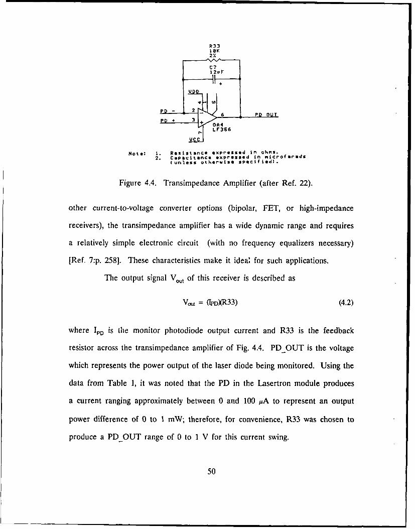
2. Transimpedance Amplifler
The second half of the receiver circuit is the preamplifier which is used
to linearly change the PD current into a voltage. This voltage is then analyzed
by subsequent stages to produce a stabilized drive current. Figure 4.4 is the
transimpedance circuit which begins the stabilization network. Compared with
49
R331OK2%
C712pF
V v
PP - 3 PD OUT
+
j
+P OUTLF366
Note: 1. Resistance expressed in oHms.2. Capacitance expressed in mcrofarads
(unless otherwise specified).
Figure 4.4. Transimpedance Amplifier (after Ref. 22).
other current-to-voltage converter options (bipolar, FET, or high-impedance
receivers), the transimpedance amplifier has a wide dynamic range and requires
a relatively simple electronic circuit (with no frequency equalizers necessary)
[Ref. 7:p. 258]. These characteristics make it ideal for such applications.
The output signal Vout of this receiver is described as
Vou = (pD)(R33) (4.2)
where IPD is the monitor photodiode output current and R33 is the feedback
resistor across the transimpedance amplifier of Fig. 4.4. PDOUT is the voltage
which represents the power output of the laser diode being monitored. Using the
data from Table 1, it was noted that the PD in the Lasertron module produces
a current ranging approximately between 0 and 100 uA to represent an output
power difference of 0 to 1 mW; therefore, for convenience, R33 was chosen to
produce a PDOUT range of 0 to 1 V for this current swing.
50

One problem with this circuit is the potential for thermal noise from the
feedback resistor R33. However, the noise from the transimpedance configuration
is less than most other receivers (except the high impedance option) and the
relatively low value of R33 reduces this problem even further [Ref. 7:p. 258].
C. DRIVE CURRENT COMPENSATION CIRCUITRY
1. Output Bias Sensor
Once the photodiode current is converted to PD_OUT, the voltage is
analyzed to determine the actual dc component (i.e., bias level) of the laser
diode's optical output. The upper half of Fig. 4.5 is the circuit used to produce
a dc voltage comparable to the drive current bias. The voltage-follower
configuration of OA5 provides buffering between the transimpedance amplifier of
Fig. 4.4 and the rest of tile compensation circuit. The low-pass filter network of
R36 and C7 then extracts the voltage ACTBIAS which represents the dc
component of PDOUT. The value of C7 was chosen large enough to maintain
a near constant bias value without oscillations over a relatively long period of
time; the charging period for such a capacitor is not a factor in this circuit since
turn-on delay safety requirements for the laser diode will exceed this time span.
The second voltage follower OA6 provides additional buffering, and the
offset nulling action of R37 compensates for any losses in this network.
2. Signal Peak-to-Peak Sensor
The voltage from the transimpedance amplifier is also analyzed to
measure the maximum fluctuation of the photodiode output (i.e., the maximum
51

10to
SOw , -in
T- I n +
'am
..
co
ae+ L
UMU
'00
W.. me:
OL NN 1L
%DM XM L.
'00
*to am..
01. 0
0a-N mum
O.5 A- I
0
01
eam.04
WIL
as 52

peak-to-peak variation of the optical output signal). Referring again to Fig. 4.5
(and as discussed in Ref. 22:pp. 232-233), the voltage PDOUT charges the
coupling capacitor C8 and thereby clamps this signal's peak negative value to zero
(i.e., ground). When PDOUT swings negative, OA7 drives D2 on, maintaining
the charge of C8. When the negative peak has passed and D2 has turned off, the
charge of C8 is still maintained since the only current drains are the inputs to
OA5 and OA6 (typically 30 pA) [Ref. 24: p. 3.2]. This results in a fast-charge,
slow-decay response to changes in the maximum fluctuation of PDOUT.
If the ac component of PDOUT is relatively large or small, the
circuitry with OA7 and OA8 may not be able to accurately clamp the signal to
grund, the.rby resulting in a biased waveform being measured for peak values
by follow-on circuitry. Figures 4.6 through 4.8 demonstrate this problem.
Figure 4.6. Properly Clamped Signal.
53

Figure 4.6 is a properly clamped waveform; the most negative peak of the sine
wave is held at ground (the solid line). The actual signal amplitude is 0.5 V and
the circuitry will produce that value.
If the amplitude of the wave is too small, as in Fig. 4.7, the negative
Ei dLIwh
Figure 4.7. Signal Clamped Above Ground.
peak may not be clamped to ground, producing an error in the measured peak-
to-peak fluctuation. The measured value is more than the actual peak-to-peak,
therefore the compensated drive signal would have less fluctuation than desired.
As shown in Fig. 4.7, the actual signal amplitude is 0.230 V; however the circuit
will measure a peak-to-peak difference of 0.295 V which includes the amount of
offset (-I-0.065 V) in the clamped signal.
If the amplitude is too big (as in Fig. 4.8), the circuit could measure a
peak-to-peak fluctuation that is less than the true value, forcing the compensated
54

drive current to be more than is desired. The 0.775 V peak-to-peak signal in
Fig. 4.8 would be measured with a 0.725 V amplitude due to the negative offset
(approximately -0.050 V) in the improperly clamped waveform.
Figure 4.8. Signal Clamped Below Ground.
Therefore, R40 and R41 are provided to allow precise clamping of
PDOUT to ground. Varying the negative supply voltage to 0A8 via R40
perfornis large, coarse adjustments to the clamp, while R41 fine-tunes the balance
to precisely adjust the clamping. By monitoring the output of 0A8 during
operation, proper clamping action can be verified. If this is not possible, R40 and
R41 can be preset to produce acceptable performance over an a priori (or likely)
range of fluctuations.
For example, according to Table 1 the Lasertron output power ranges
between 0 and 1.0 mW; this corresponds to a photodiode current of 0 to 95.0 pA
which results in a PDOUT voltage from Fig. 4.4 of approximately 0 to 1.0 V.
55

After adjusting R40 and R41 to the median expected signal (i.e., 0.5 V from
PDOUT), accurate clamping of peak-to-peak signal amplitudes between 0.370 V
and 0.735 V (a - 26% to +47% range in maximum signal values without
noticeable error) can still be realized. This median value can, of course, be
changed as required. However, care must be taken to ensure the negative swing
of the analog signal does not drive the laser diode drive current below its
specification-sheet threshold value. Although this stabilization network will
compensate for changes in 'TH due to aging and heat, user-specified peak-to-peak
levels which are too large or bias settings which are too low will adversely affect
the action of this circuitry.
The clamped signal can now easily be measured to determine the
maximum PDOUT voltag-' differential, which represents the maximum optical
output difference from the laser diode. In Fig. 4.5, C10 is used to store a dc
voltage equal to the peak of the clamped signal from OA8. To accomplish this,
OA9 drives D3 on when the slope of the clamped signal goes positive; the rising
signal charges CIO to the peak voltage and the capacitor holds this value even
when the slope of the clamped input goes negative. As recommended in
Ref. 22:p. 254, CIO is made of polystyrene to ensure low leakage and low
dielectric absorption and thereby to accurately maintain the desired peak voltage
value.
The bleed resistor R46 is used to develop another fast-charge, slow-
decay response. Circuit settling times are minimized by C9; configured as shown
in Fig. 4.5, the circuit arrives within 0.1% of the true peak value within 10 ps or
56

less. Finally, R44 helps to prevent overdrive damage to OA9 from C10 when the
supply voltages are switched off. [Ref. 22:pp. 254-255]
Two inverting gain amplifiers, OA10 and OAll, are used to compensate
for losses within this peak-to-peak detector circuit (and within follow-on stages)
and to maintain (with the help of Cll) a stabilized dc output [Ref. 22:p. 402].
Together they produce ACTPKPK, the voltage which represents the maximum
fluctuation in optical power detected by the photodiode in the laser diode module.
3. Bias Compensation Circuit
Once the actual signal bias level is measured (as represented by the
voltage ACTBIA0 from Fig. 4.5), this value must be compared to a desired
output bia. level. This comparison is used to produce a compensated bias signal
which represents the amount of drive which must be supplied to the laser diode
in order to increase or decrease the optical output to achieve the desired bias
level. Although this circuit produces a compensated voltage, this voltage is
converted into a drive current by a voltage-controlled current source in a
subsequent stage. Figure 4.9 is the circuit used to produce this compensated dc
signal.
The desired bias level is set by R52; using the components shown, the
wiper voltage swing is 0 to L. V, which represents a 0 to 1.0 mW output signal
bias variation. To increase/decrease tnis range, R51 can be decreased/increased.
The differential amplifier configuration of OA12 produces a voltage comparable
to the difference between the actual and desired optical power bias levels. Care
57

CD
a..
U) MDa, I( a I
000OCU
I +z
Ic N (n
(Dr(4,D m C
58 1
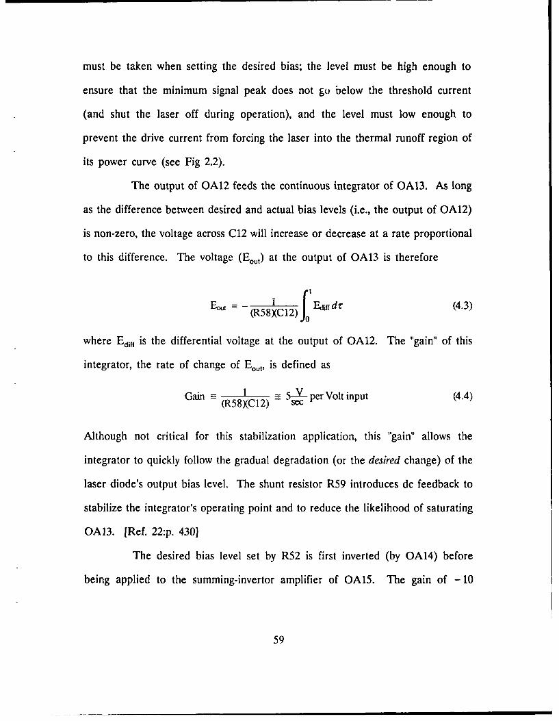
must be taken when setting the desired bias; the level must be high enough to
ensure that the minimum signal peak does not go below the threshold current
(and shut the laser off during operation), and the level must low enough to
prevent the drive current from forcing the laser into the thermal runoff region of
its power curve (see Fig 2.2).
The output of OA12 feeds the continuous integrator of OA13. As long
as the difference between desired and actual bias levels (i.e., the output of OA12)
is non-zero, the voltage across C12 will increase or decrease at a rate proportional
to this difference. The voltage (Eout) at the output of OA13 is therefore
Eouw - - 1 Ediadr (4.3)(R58XC12) E d(
where Edi" is the differential voltage at the output of OA12. The "gain" of this
integrator, the rate of change of Eout, is defined as
Gain - 1 = per Volt input (4.4)(R58XC12) sec
Although not critical for this stabilization application, this "gain" allows the
integrator to quickly follow the gradual degradation (or the desired change) of the
laser diode's output bias level. The shunt resistor R59 introduces dc feedback to
stabilize the integrator's operating point and to reduce the likelihood of saturating
OA13. [Ref. 22 :p. 4301
The desired bias level set by R52 is first inverted (by OA14) before
being applied to the summing-invertor amplifier of OA15. The gain of - 10
59

induced by R65 and R69 (negative gain since this voltage will be applied to a
summing-inveror amplifier) is due to the current-to-optical power ratio of the
diode during lasing. Table 1 indicates that this ratio for this particular device is
approximately
Al _ 45 mP-35 mA 10 A-W 1 (4.5)AP 1 mW
Consequently a gain factor of 10 is used when formulating the desired bias level
(which is actually represented in mW) and computing the required drive current.
If this current-to-power ratio is different than 10:1 for the laser diode being used
with this circuit, R65 must be altered as needed to produce the expected results.
A voltage which corresponds to the laser diode's threshold current is set
by R67 in Fig. 4.9. The wiper voltage can vary between -1.0 V and 0 V which
represents a threshold current range of 0 to 100 mA (the variation is over
negative voltage since this will be used in a summing-invertor amplifier); this range
can be increased/decreased by decreasing/increasing R66. This value of threshold
current is obtained from the particular laser diode's specification sheet
(e.g., Table 1) and is set during circuit start-up procedures.
Finally, these three representative voltages--the desired bias level, the
difference between the desired and measured levels and the value representing a
particular laser diode's threshold current--are summed in OA15. The result is the
voltage COMPBIAS which corresponds to the compensated bias current level
necessary to achieve the desired average optical output from the laser diode.
60

4. Automatic Gain Control Circuit
In order to achieve dhe desired maximunm peak-to-peak fluctuation in the
optical output of the laser diode, the peak measured variance (from the circuit in
Fig. 4.5) must be compared to a desired value, and the actual modulation input
amplified or attenuated accordingly. These comparisons and modifications are
accomplished by the circuit in Fig. 4.10.
The desired maximum swing in optical power is set by R71; the wiper
voltage varies between 0 and 0.1 V, representing a power variation between 0 and
1.0 mW. The range of vnltages representing this desired value is one-tenth the
range of ACTPKPK, the true power variance; this increas..d gain factor of ten
is inherent in the output of the divider configuration of OA16 [Ref. 25:p. 6.18].
This range can be increased/decreased by decreasing/increasing R72. Again care
must be taken when setting the desired peak-to-peak variation; the fluctuation
must not allow the laser to shut off (i.e., force the drive current below threshold)
or to enter its thermal runoff region (see Fig. 2.2).
The output of OA16 represents the ratio of the desired peak optical
power fluctuation to the measured value. This ratio can be as large as ± 10 and
is limited only by the electrical capabilities of the AD534 [Ref. 26:p. 6.28].
However, the inputs of OA17 are restricted to the range of ±1.0 V
[Ref. 25:p. 6.44]. Therefore, the output of OA16 is sent through a voltage divider
(R73 and R74) to ensure that OA17 is not overdriven.
The computed ratio is then used to modify the actual input signal
(applied across pins 1 and 2 of OA17) via the wideband, dc-coupled multiplier
61

Ca-
w -O
um10
to " m7L.
-4- Z 04
CD
& N & (
a v c
-U EMr. -u
at 0
LaM,*M
626

network of OA17 and OA18. Since inputs of OA17 are limited to ± 1.0 V (as
noted above), an input signal fluctuation of 1.0 V should correspond to the
maximum output power swing from the laser diode being driven. In this design
case, using the Lasertron specifications described in Table 1, a 1.0 V peak-to-
peak input signal would represent a 1.0 mW optical signal fluctuation. As an
illustrative example, if a peak-to-peak fluctuation of 0.5 mW was required from
the laser diode, the wiper voltage of R71 would be adjusted to 0.05 V and the
input signal would require a peak-to-peak fluctuation of 0.5 V. The compensation
circuitry would then modify the input signal to take into account the module's
aging and temperature effects as noted by the current from the monitor
photodiode. If the peak power of the laser diode is different than the Lasertron
being used in this design, the 1.0 V peak input could readily represent a larger
(or smaller) maximum optical output by changing certain amplifier resistors in the
subsequent final summing amplifier stage.
It must be noted that this network is not designed to modify the input
modulation signal, i.e., to amplify (or attenuate) a weak (or strong) electrical
signal. Although the automatic gain control circuitry can be used to artificially
boost a weak input signal, the system is intended to stabilize the optical output
of the laser diode being driven; it assumes that the incoming electrical signal from
the signal generator is of the correct strength to produce the desired peak-to-peak
power fluctuation; i.e., if a 0.5 mW peak-to-peak fluctuation is desired, an input
signal of 0.5 V is assumed at pins 1 and 2 of OA17.
63

As configured in Fig. 4.10, the full-scale swing at the output of OA18
is ± 1.0 V and is accurate to within 1% [Ref. 25:p. 6.471. Due to the divider
network of R73 and R74 and the gain in the OA17 and OA18 circuitry, this
voltage represents one-fifth the necessary signal to drive the laser diode and
achieve the desired optical power fluctuation. The signal is amplified in the next
stage.
The voltage-follower configuration of OA19 provides for stabilization of
the compensated input signal and helps to impedance-match the circuit of
Fig. 4.10 to the final summing stage.
5. Final Summing Circuit
All that remains to be done in the compensation circuitry is to combine
the bias and modulation signals in a summing network. Figure 4.11 is such a
network, with the compensated signals COMPBIAS and COMP_PKPK being
R84 R8620K 20K
COP BIAS XI
C 19 RS
2.Cpctn. exr.sd n 2~cOKa'a
4F 22K Fia R
45 OA21
-- - Cie1.0
Note: 1. Resistance expressed in ohms.2. Calpacitalnce expressed in micro(Brads.
Figure 4.11. Final Summing Circuit (after Ref. 22).
64

combined in the summing-invertor OA20. Resistors R85 and R86 supply the gain
which is required for the amplified peak-to-peak signal as discussed in the
paragraph above; the coupling capacitor C17 removes any stray dc signal which
may be in COMP_PKPK. It is R85 which can be changed to produce different
power fluctuation levels for 1.0 V inputs to OA17 (see Fig. 4.10); a laser diode
with a peak output power of 3.0 mW would use a value one-third of that shown
for R85 in Fig. 4.11, a peak power of 0.5 mW would need a resistor twice that
shown, and so on. Obviously, the specification sheet of the laser diode being
driven must be referenced and the proper value of R85 inserted prior to operation
in order to maintain the proper relationships between desired power fluctuation
as set by R71, the peak-to-peak fluctuation of th: imput signal and the optical
output of the laser diode.
Finally, since OA20 creates an inverted signal, OA21 is used to produce
the necessary positive waveform COMPSIG.
D. DRIVE "CURRENT" LIMITER
In order to provide overload protection for the laser diode, the series
clipping circuit of Fig. 4.12 is included in stabilization network. The wiper voltage
of R89 is used to set the "current" limit; since the signals being processed are
voltages, this circuit does not really limit current but limits the voltage which will
be used to produce the drive current in the next stage. The wiper of R89 can
vary between 0 and 5.0 V, corresponding to a current limit range of 0 to 500 mA;
care must therefore be taken to set a proper limit so as not to negate the effect
65

of the series clipper. The range of limits can be decreased by including a resistor
between R89 and VCC or can be increased by using a higher voltage than VCC
sourcing R89.
ROB
2%KNoe C2. Ce222tace ex s6 -e C L I Pd A4 SIG
2. pC e rr LF356S
o A222 L 2 e 4 I O A" 0 2 362
EL241
(COMP _IG or t e l m t s t b R8 -is .le s t Ia s t h i p t o h ot g
r,- co N 9 1 4 D I S
1IN914
--- 1 C2
Note: I. Resistance exp essed in ohms.
2 , C c p ac t n c e e x p e s s e d i n m i cr: o fa r md s .
Figure 4.12. Drive "Current" Limiter (after Ref. 22).
The two diodes (D4 and D5) connected to OA22 and OA23 perform a
gating function for the compensated signal, allowing whichever voltage
(COMPSIG or the limit set by R89) is less to pass to the input of the voltage
follower OA24; this combination is therefore labelled the "Linear-OR Gate"
[Ref. 22:p. 229). Whenever COMPSIG falls below the set limit, OA23 turns D5
off and COMPSIG is passed directly through to OA24. If COMPSIG exceeds
the limit, OA22 turns D4 off and the set limit voltage appears at the voltage
follower OA24.
66

To realize a high-speed (100 kHz or more) clipper, OA22 and OA23 must
necessarily have extremely fast response times and slew rates to produce the
proper clipped, compensated drive signal (CLIPSIG) to the next stage. The
EL2041, with a 90 MHz bandwidth, 250 V/Ms slew rate and 90 ns settling time
(to within 0.05% of final value), is ideal for this application [Ref. 27:p. 1.135].
Figure 4.13 demonstrates the results of this clipping circuit; the wiper voltage
EEEEEE
Figure 4.13. Clipped Signal.
of R89 was set at 0.480 V (corresponding to a current limit of 48.0 mA). The
minimum overshoot noted in Fig. 4.13 (0.020 V) was constant for all clipping
limits. Excellent response was achieved for high speed signals (here at 100 kHz)
due to the capabilities of the EL2041 used for both A22 and A23.
67

E. SURGE PROTECTION
Laser diodes are extremely susceptible to current spikes which may appear
in the drive current; therefore, some buffering is needed between the network's
external power supply and current-producing stage. This buffer acts as a "slow-
on slow-off' network to prevent these surges from reaching the laser diode during
powering up/down of the circuits or in the case of an unscheduled power
interrupt.
Figure 4.14 demonstrates the desired supply voltage-versus-time relationship
0>
Timeti t 2 t3 t4
Figure 4.14. "Slow-on Slow-off' Power Supply.
for the surge protector. At some time t,, external power is connected to the
circuit (i.e., turned "on"), and the output of the slow-start circuit "slowly" increases
to its maximum value (+ 15 V for this network) at t2. The term "slowly" is
relative; current spikes are on the order of a few pico- or nanoseconds in duration
and voltage transients usually disappear after a few milliseconds, therefore several
milliseconds delay between t1 and t 2 will be sufficient to prevent harmful surges.
68
At t3, power is disconnected (either intentionally or not) and the "slow-off' system
"gradually" reduces (again during a few milliseconds) the voltage to 0 V.
Figure 4.15 is derived from Ref. 20:p. 2.14. By closing switch S1, LED Li
indicates external power is connected; consequently Li acts as an indicator of
+15 St VR4T .M317K
Fige.1. "Vin +Souw-off +Cc SL0U
L-o I R92
R03 49. 9K"> , R90 _ C24
". -- -- 2S
Note: 1. ResistaInce expressed in ohms.2. Capaicitalnce expressed in microfaralds.
Figure 4.15. "Slow-on Slow-off' Circuit (after Ref. 20)
power failure. Simultaneously, regulator VR4 slowly charges C24. When S1 is
opened (or the + 15 V power is otherwise interrupted) C24 slowly discharges
through the Q3, VR4, R91, R92 and D6 network, thereby providing a slowly
decreasing voltage source.
F. VOLTAGE-TO-CURRENT CONVERTER CIRCUIT
With a voltage available which represents the laser drive current necessary
to obtain the desired optical output (CLIPSIG), a conversion circuit is necessary
to actually produce the required supply current. Figure 4.16 serves as a general-
purpose, low-power voltage-controlled current source. The sensitivity of the
69

voltage-to-current conversion is inversely proportional to the quality of R93;
consequently, a prerision-type resistor (in this case a 2% wire-wrapped device) is
required for high accuracy.
D)7IN4085
+15R9o I R95
2%8G 28K3
R97 R98
1.o1K 1. Re" R94 ' e [- 10 OA26 +15 SLOU_ 2U 2
2.2 LaaiF ne356se I iroaas
62N2219
4780
Irl - , c LASER+
DS R991N4eO5 I
-15 2
Note: a. Resistance expressed in ohms.2. C1acitance expressed in icrofarads.
Figure 4.16. Voltage-Controlled Current Source (after Ref. 22).
The laser diode drive current Ioc is determinedd by
ILD = CLPSG(4.6)R70
The voltage CLIP-SIG will typically vary between 0.35 V and 1.00 V (using the
data available from Table 1), therefore the current supplied to the laser diode
must necessarily range between 35 mA and 100 mA; currents which are much
greater than 100 mA will possibly result in a catastrophic degradation of the laser
diode's output and should therefore be limited by the circuit of Fig. 4.12. Since
OA25 has a rated current of only 25 mrA (verified by experimentation), a boosted
output configuration for the cut-rent source is needed. Transistor Q4, rated at
100 mA with a 300 MHz bandwidth [Ref. 28:p. 4.93], is sourced from the "slow-
70

start" + 15 V. Relay K1 is included to allow an even greater delay in the drive
current during power-up and a quicker disconnect of current during power-down.
Diodes D7 and D8 prevent potentially damaging reverse currents from reaching
the laser diode. R99 facilitates the monitoring of the actual drive current; by
placing a voltmeter across the 1 n resistor, the dc and ac components of the
supply current can be measured.
As shown in Fig. 4.16, the laser anode will be connected to the point
LASER - and cathode to IASER_+. The current from OA19 will then
modulate the forward-biased laser diode, which produces a current in the reverse-
biased monitor photodiode and closes the power stabilization network loop.
G. SUMMARY
Although laser diodes have demonstrated extremely long lifetimes, their
transfer functions (of changing electrical power into optical power) are greatly
affected by age and operating environment. As devices get older or operate at
changing temperatures, varying levels of drive current are required to produce the
same level of optical power as new, temperature-stabilized diodes. In order to
maintain a consistent performance throughout a laser diode's lifetime, the drive
current must be continually monitored and (if necessary) modified to produce the
desired optical power modulation. This stabilization network will compensate for
most effects of gradual degradation and, with a signal clipping circuit, will help to
reduce the likelihood of a catastrophic failure.
71
V. TEST AND EVALUATION
A. INTRODUCTION
Both stabilization networks--cooling and power--were subjected to several
tests to evaluate their capabilities to drive a laser diode in steady-state conditions.
By supplying various signal waveforms (sine/triangular/square waves at several
frequencies) and by varying desired output parameters (device temperature, optical
signal bias and modulation levels), the theoretical circuit design was evaluated
regarding stability and dynamic range.
B. EVALUATION PROCEDURE
1. Test Equipment and Set-up
Figure 5.1 is a block diagram of the equipment used and the
interconnections necessary in the system evaluation. A Wavetek Model 143
generates the modulated test signal to the power stabilization network. Both
networks provide input to the Optologic TF-DIP Laser/LED test fixture which
cradles the laser diode and provides a convenient method of obtaining feedback
regarding module temperature and output power levels. Care must be taken to
ensure the laser diode module's 14-pin DIP layout matches that of the Optologic
fixture; different pin outlines might result in circuit damage or catastrophic failure
of the module. The pigtail output of the laser diode is fed to a Photodyne Model
1600XP optical waveform analyzer which produces a voltage comparable to the
72

TEKTRONIXModel 2465A Channeloscilloscope =ED
PHOTODYNE WAVETEKModel 1600XP Model 143pcalnaer function generator
OPTOLOGICTF-DIP
LASER/LED
"] B ias Peak
Set-point LLevel Fluctuation
Temperature 0 0 PowerDrive Stabilization
___ Threshold Current NetworkTemperature Current Limit
Stabilization 0 0Network
Figure 5.1. Test Equipment Set-up.
incident optical signal. This electrical signal, along with the monitor photodiode
and original signal, are displayed on a Tektronix Model 2465A oscilloscope.
2. Operating Procedures
a. Start-up
To ensure safe operation of the laser module, this start-up
procedure should be followed:
73
* Connect test equipment as shown in Fig. 5.1.
" Ensure that switch S1 is open (LED L1 should be off).
" Energize external power (_t15 V dc and ±5 V/1 A dc sources).
• Adjust set-point temperature to desired operating point by setting the wipervoltage of R10 to the desired operating temperature accordirg to Eq. 3.10.
* Decrease the wiper voltage of R67 to set the threshold current as specifiedin the laser diode's data sheet; the wiper voltage varies between 0 and-1.0 V which corresponds to a threshold current range of 0 to 100 mA.
" Ensure that the wiper voltages of R52 (optical bias) and R71 (desired peak-to-peak optical fluctuation) are set to 0 V.
• Adjust R89 to set the necessary current limit level; the wiper voltage of R89ranges between 0 and 5 V, corresponding to a current limit of 0 to 500 mA.
* Close S1 (L1 will light); after a few seconds, relay Ki will close allowingcurrent to flow to the laser diode.
Set the modulated signal amplitude fluctuation (via the Wavetek attenuationverniers) to the value corresponding to the desired optical power fluctuation(e.g., a 1.0 V peak-to-peak variance in input signal results in a 1.0 mW peak-to-peak fluctuation in the Lasertron module's output).
* Increase the wiper voltage of R52 to set the desired bias level; the wipervoltage varies between 0 and 1 V corresponding to a signal bias variation of0 to 1.0 mW.
" Increase the wiper voltage of R71 to set the desired maximum variation inthe modulated optical signal; the wiper voltage ranges between 0 and 0.1 Vcorresponding to a power fluctuation of 0 to 1.0 mW.
The reason that all power levels are initialized to zero prior to
connecting the laser diode is one of device safety. With the laser diode
disconnected, there is obviously no monitor photodiode signal entering the power
stabilization network. If desired power levels were indeed specified at values
greater than zero by R52, R67 or R71 prior to the connection of the laser diode
74

module, the integrator (OA13) would attempt to match its output to the non-
existent monitor photodiode signal. Therefore, the output of the integrator could
quickly saturate at several volts. Depending on the limiting value set by R89, this
could lead to a bias current of several hundred milliamps being applied to the
laser diode when S1 is closed and may result in a catastrophic degradation of the
module. Consequently, desired operating levels are set after the laser diode
module is connected to the network.
b. Laser Diode Modulation
The output waveforms on the oscilloscope should be closely
monitored to ensure desired power levels are not exceeding the capability of the
laser diode being tested. Temperature, signal bias and fluctuation levels can be
varied to observe the effect on the optical waveform.
c. Shut-down
Whether powering-down of the networks is intentional or
unintentional, the steps for a proper system shut-down are:
" Open SI (L1 turns off).
" Reset the wiper voltages of R67 (threshold current), R52 (optical bias) andR71 (desired fluctuation) 0 V.
" Disconnect modulated test signal.
" Disconnect external power (t.15 V dc and ±5 V/1 A dc sources).
75

C. DRIVING THE LASER DIODE WITH DC SIGNALS
1. Without Temperature Stabilization
Using only the power stabilization network, a dc drive current was
applied to the laser diode in increasing levels from 0 to approximately 100 mA.
Threshold current was set to -0.35 V (by R67) to correspond to the specification
sheet threshold current of 35 mA, and the desired peak-to-peak fluctuation was
set to 0 (at R71) to indicate a dc output is desired; no external signal was applied
to the network (via OA17). Then by increasing the desired bias level (at R52),
the unmodulated optical output can be changed. The drive current was monitored
by the voltage drop across the 1 n resistor R99; an ammeter was used to display
monitor photodiode current and thermistor resistance was read from an ohmmeter
across the module's thermistor leads (since the cooling network was not
connected). The actual optical output was converted by the Photodyne analyzer
and displayed on the Tektronix oscilloscope. The Photodyne analyzer required
approximately five minutes of warm-up time before readings could be taken; the
analyzer produced an output of nearly -2.8 mV without an optical input, and the
five minutes allowed the analyzer's output to stabilize at approximately 0 inV.
Table 3 shows the results of this test. As can be expected, the trace on the
oscilloscope was extremely "fuzzy" at lower output levels (less than 0.040 mW)
since the laser diode is acting as an LED and not emitting coherent light with a
narrow spectral width. As noted earlier, the increasing module temperature also
affects the operation of the photodiode and small signals can be lost in such noise.
76

TABLE 3. RESPONSE WITHOUT TEMPERATURE STABILIZATION
Drive Optical Photodiode Thermistor'Current (mA) Output (mW) Current (mA) Resistance (kn)
3.6 0.0 0.0003 11.3710.5 0.0 0.0005 11.0515.0 0.0 0.0007 10.9320.8 0.006 0.0011 10.7125.0 0.010 0.0013 10.5930.0 0.012 0.0017 10.3935.0 0.016 0.0024 10.2236.3 0.018 0.0028 10.1637.0 0.022 0.0030 10.0238.0 0.024 0.0040 9.9939.0 0.040 0.0100 9.9040.0 0.062 0.0186 9.8641.0 0.084 0.0283 9.8242.0 0.104 0.0384 9.7843.0 0.128 0.0486 9.7544.0 0.154 0.0601 9.6945.0 0.178 0.0694 9.6646.0 0.204 0.0777 9.6047.0 0.226 0.0862 9.5648.0 0.246 0.0968 9.5349.0 0.270 0.1073 9.5150.0 0.292 0.1169 9.4251.0 0.320 0.1245 9.4052.0 0.345 0.1333 9.3753.0 0.365 0.1432 9.3454.0 0.385 0.1526 9.3055.0 0.410 0.1619 9.2860.0 0.510 0.2045 9.1565.0 0.610 0.2459 &9970.0 0.690 0.2815 8.7675.0 0.780 0.3149 8.5380.0 0.870 0.3450 8.3685.0 0.930 0.3729 8.19
But once the drive current exceeded threshold, the optical power levels became
very distinct. Figure 5.2 is a plot of the measured output power versus drive
current; it has the classic form of a laser diode transfer function (see Fig. 2.2).
77

CC
EN%
0 0i
z Hl
o>N 74
- .U
rn0
00
z
01T 8*0 9,0 f0o 2 oO
(SJIJviwvIN) HUZIMOd Lfld~flO
78

The measured photodiode activity is shown by the solid line in Fig. 5.3.
Using linear regression and a least-squares fit, the data from Table 3 was modeled
as
Output Power = 2.5 W-A:-(Photodiode Cunent) (5.1)
In other words, the tnured photodiode responsivity R is
R - 1 0.4 A-W- 1 (5.2)2.5 W-A- '
This value is four times the specification sheet value (see Eq. 4.1). Consequently,
in order to maintain the design criterion of a 1.0 V maximum output from OA4
(PDOUT), R33 was changed from 10.0 ko to 2.5 kn; i.e.,
PDOUTmax = (IpE=)(R33) =_ (0.4 mA)(2.5 kW) = 1.0 V (5.3)
This change preserves the basic assumptions behind the remainder to the power
stabilization network.
Without temperature stabilization, it was expected that the thermistor
resistance would decrease as the laser diode's output power increased. This was
confirmed by the data in Table 3; Fig. 5.4 is a plot of the thermistor resistance
versus output power. Using this data and Eq. 3.5, Fig. 5.5 was created which
shows the relationship between module temperature and output power. It can be
seen that the laser diode temperature quickly increased with little change in
output and then gradually increased as the output increased. Consequently, this
temperature variation affected the transfer function plotted in Fig. 5.2; this effect
79

0D
-t
0 4
1-a-
o In
Ho H
Cl)
800

can be negated by connecting the temperature stabilization network designed in
Chapter III.
NO TEMPERATURE STABILIZATIONE-
I ,tI I I
0.0 0.2 0.4 0.6 0.8 1.0
OUTPUT POWER (MILLIWATTS)Figure 5.4. Thermistor Resistance versus Output Power.
0
HNO TEMPERATURE STABILIZATIONC;
0.0 0.2 0.4 0.6 0.8 1.0OUTPUT POWER (MILLIWATTS)
Figure 5.5. Module Temperature versus Output Power.
81

One final test was needed to compare the accuracy of the desired bias
level to the actual optical output as measured on the oscilloscope. The wiper
voltage of R52 was adjusted between 0.0 V and 0.9 V, representing a desired
optical bias level of 0.0 mW to 0.9 mW. At the same time, the Photodyne
analyzer output was monitored on the oscilloscope and on a digital voltmeter; with
these devices, a 0.0 mV to 0.1 mV range represents a 0.0 mW to 1.0 mW laser
diode output. The result of this test are shown in Table 4.
TABLE 4. DESIRED VERSUS ACTUAL OPTICAL OUTPUT BIAS LEVELS
Desired ActualOptical Output (mW) Laser Diode Output (mW)
0.0 0.00.1 0.0850.2 0.1800.3 0.2800.4 0.3750.5 0.4600.6 0.5650.7 0.6500.8 0.7350.9 0.840
As can be seen, there is an offset of approximately -0.015 mW to -0.060 mW
between desired and actual power levels; this difference can be explained by the
approximation used in the transimpedance amplifier circuit and by the input offset
voltages of the unbalanced op-amps used throughout the network [Refs. 24:p. 3.2
and 27:p. 1361. Although the offset is small and can be easily dealt with during
operations, attempts were made to eliminate these differences. This could be
82

accomplished by altering summing ratios or op-amp biases somewhere within the
whole network. However, changing resistor ratios in the network after the bias
compensation circuit (Fig. 4.9) would also -ffect the peak-to-peak compensation
values. Tht.refore, the problem would have to be dealt with solely by
manipulating the elements in the bias compensation circuit. By altering the input
resistances within the circuit, greater error was introduced. The only suitable
results occurred when the offset voltage potentiometers in Fig 4.9 (R57, R64 and
R70) were altered to reduce the difference between desired and actual output.
Unfortunately, changing the offset nulls of ihe op-amps resulted in the saturation
of the OA13 integrator at 4.5 V during power-up. This meant a surge of 450 mA
through the laser diode when relay K1 was closed. To prevent such a dangerous
situation, the op-amps of Fig. 4.9 were rebalanced by returning the nulling
potentiometers to their original values. The differences noted in Table 4 would
have to be taken into account during operation.
2. With Temperature Stabilization
The same test procedures were conducted on the laser diode as before,
however the cooling network was activated and the module operating temperature
was varied to determine its affect on optical output. The desired operating
temperature was set by adjusting the wiper voltage of R10 according to Eq. 3.10.
The current to the TEC was then allowed to stabilize before applying drive
current. This brief period would allow the module to reach the desired operating
temperature before output power began increasing (which increases the
83

temperature of the module as shown in Fig. 5.5). The wiper voltages and stable
TEC currents used for the test are shown in Table 5.
TABLE 5. TEMPERATURE STABILIZATION TEST VALUES
Desired Operating RIO Wiper Stabilized TECTemperature (C) Voltage (V) Current (mA)
15.0 i.2 98.120.0 1.4 26.325.0 1.6 -32.230.0 1.8 -32.2
The stabilized TEC current levels were necessary to offset the difference between
set-point and ambient (22.5 C) temperatures. With a desired temperature higher
tl, .n ambient, the TEC current was actually heating the module. This heating
current peaked at -32.2 mA since this is the maximum value allowed from the
-5 V/1 A source through R30 (see Fig. 3.6); this reverse-biased current was
limited to this maximum to prevent damage to the TEC.
Table 6 shows the results from the drive currents applied to the laser
diode stabilized at four different operating temperatures. Figure 5.6 displays this
data plotted on a single graph; as discussed in Chapter 'I, an increase in set-point
temperature from 15 C to 30 C results in an iacrzase in threshold current from
approximately 32.0 mA to 40.0 mA. There is however, little change in the slope
of the lasing region of the four graphs.
The monitor photodiode current was also noted during the stabilization
test to detect any dependence of responsivity to set-point temperature; Table 7
shows these results and Fig. 5.7 displays the data on one graph. The nearly
84

TABLE 6. TEMPERATURE-STABILIZED LASERTRON RESPONSE
Optical Output (mW)Drive
Current (mA) 15 C 20 C 25 C 30 C
0.0 0.0 0.0 0.0 0.09.0 0.016 0.006 0.0 0.008
15.0 0.024 0.016 0.0 0.01420.0 0.030 0.020 0.0 0.02025.0 0.036 0.026 0.004 0.02230.0 0.038 0.030 0.009 0.02635.0 0.076 0.032 0.013 0.02836.0 0.100 0.038 0.016 0.02837.0 0.122 0.064 0.018 0.03038.0 0.148 0.092 0.022 0.03239.0 0.174 0.116 0.035 0.03440.0 0.202 0.140 0.060 0.03441.0 0.226 0.166 0.086 0.03842.0 0.250 0.190 0.110 0.04843.0 0.274 0.212 0.136 0.07044.0 0.300 0.238 0.162 0.09245.0 0.330 0.260 0.188 0.12246.0 0.350 0.284 0.210 0.14847.0 0.375 0.312 0.236 0.17248.0 0.400 0.340 0.260 0.19249.0 0.425 0.365 0.285 0.21650.0 0.440 0.385 0.310 0.24055.0 0.555 0.510 0.425 0.36560.0 0.680 0.625 0.540 0.47565.0 0.760 0.710 0.640 0.58070.0 0.870 0.830 0.740 0.68075.0 0.950 0.900 0.820 0.77080.0 1.000 0.990 0.910 0.86085.0 1.000 1.020 0.990 0.940
coincident lines indicate the monitor photodiode's responsivity is nearly constant
over "normal" operating temperature ranges. This simplifies the total network
design by alleviating the need to compensate the photodiode output current for
temperature differentials.
85

TABLE 7. TEMPERATURE DEPENDENCE OF PHOTODIODE CURRENT
Photodiode Current (mA)/Optical Output (mW)
15 C 20 C 25 C 30 C
0.0002/0 0.0003/0 0.0002/0 0.0002/00.0005/0.016 0.0005/0.006 0.0005/0 0.0005/0.0080.0009/0.024 0.0008/0.016 0.0007/0 0.0008/0.0140.0012/0.030 0.0011/0.020 0.0011/0 0.0010/0.0200.0016/0.036 0.0014/0.026 0.0014/0.004 0.0013/0.0220.0022/0.038 0.0019/0.030 0.0017/0.009 0.0016/0.0260.0188/0.076 0.0034/0.032 0.0024/0.013 0.0021/0.0280.0306/0.100 0.0053/0.038 0.0026/0.016 0.0022/0.0280.0421/0.122 0.0167/0.064 0.0031/0.018 0.0024/0.0300.0544/0.148 0.0282/0.092 0.0039/0.022 0.0026/0.0320.0661/0.174 0.0393/0.116 0.0097/0.035 0.0028/0.0340.0769/0.202 0.0504/0.140 0.0203/0.060 0.0032/0.0340.0890/0.226 0.0616/0.166 0.0307/0.086 0.0040/0.0380.1005/0.250 0.0718/0.190 0.0420/0.110 0.0082/0.0480.1112/0.274 0.0825/0.212 0.0528/0.136 0.0175/0.0700.1220/0.300 0.0937/0.238 0.0628/0.162 0.0273/0.0920.1336/0.330 0.1045/0.260 0.0724/0.188 0.0380/0.1220.1440/0.350 0.1150/0.284 0.0825/0.210 0.0481/0.1480.1548/0.375 0.1260/0.312 0.0924/0.236 0.0588/0.1720.1661/0.400 0.1378/0.340 0.1031/0.260 0.0686/0.1920.1781/0.425 0.1480/0.365 0.1132/0.285 0.0787/0.2160.1887/0.440 0.1586/0.385 0.1242/0.310 0.0877/0.2400.2425/0.555 0.2101/0.510 0.1747/0.425 0.1352/0.3650.2939/0.680 0.2608/0.625 0.2223/0.540 0.1811/0.4750.3459/0.760 0.3084/0.710 0.2685/0.640 0.2238/0.5800.3901/0.870 0.3515/0.830 0.3097/0.740 0.2651/0.6800.4369/0.950 0.3968/0.900 0.3522/0.820 0.3023/0.7700.4520/1.000 0.4338/0.990 0.3880/0.910 0.3391/0.860
0.4518/1.020 0.4248/0.990 0.3705/0.940
86

0<0E--N
g= L -
o 1: +a
(SILLV~t~rl"IIN) NHAdJl~l
87E

mOC~
00
0
oD
T-o0*0 0'
(Sd4VIIlI) HA~dLf~~f0
880

D. MODULATING THE LASER DIODE
1. Verifying Network Design
An external modulation signal was connected to the stabilization
networks (both power and temperature) and the laser diode was tested with
various waveforms of different frequencies. Figure 5.8 is a typical optical
waveform as transformed the Photodyne analyzer into an electrical signal; with a
desired bias level of 0.5 mW at a frequency of 100 kHz, a sine wave was sent
through the laser diode producing a 50.0 mV biased, 100 kHz modulated signal.
t
Figure 5.8. Modulated Laser Diode Output.
As was done with the dc bias level adjustment, a test was conducted to
verify the correlation between desired peak-to-peak fluctuation (as set by R71 in
Fig. 4.10) with the actual output observed on the oscilloscope. The waveform of
Fig 5.8 was used in this experiment; with the desired bias level set at 0.5 mW,
89

the frequency kept at 100 kHz and the temperature stabilized to 25 C, the input
signal amplitude was varied (using the Wavetek). The desired fluctuation level
was set via the wiper voltage of R71; the variation of 0 to 13 mV corresponded
to a 0 to 1 mW peak-to-peak power fluctuation. It was quickly seen that the
optical output from the stabilization network was greater than the desired
fluctuation by a factor of two; therefore, R85 (Fig. 4.11) was changed from 2.0 kn
to 4.22 kn to correct the problem. Table 8 shows the comparisons of desired to
realized power fluctuation obtained in this experiment before and after changing
R85.
TABLE 8. DESIRED VERSUS ACTUAL OUTPUT POWER FLUCTUATION
Actual Output Fluctuation (mW)
Desired Fluctuation (mW) R85 = 2.0 ko R85 = 4.22 ko
0.05 0.100 0.0520.10 0.215 0.1060.15 0.320 0.1900.20 0.420 0.2180.25 0.540 0.2620.30 0.3220.40 0.4260.50 0.5350.60 0.6250.70 0.7350.80 0.8100.90 0.900
The remaining error in results can be attributed to the approximation used in the
transimpedance amplifier circuit.
90

It should be noted that measurements were difficult to make at the
extremes of the optical output; the low power levels (less than 0.190 mW)
produced traces on the oscilloscope which were extremely "fuzzy" while the higher
power levels (above 0.8 mW) resulted in waveforms with jitter. This "fuzziness"
may be aue to the fact that the dc bias applied to the laser diode was not large
enough to produce a sharp output; experiments have shown that drive currents at
or near threshold can show significant output distortion while small increases in
the bias current greatly improve the "cleanliness" of the optical output
[Ref. 2 9 :p. 247]. The solution to this problem may seem obvious: increase the
dc bias. Unfortunately, this technique results in the second noted distortion, that
of jitter. Laser diodes tend to exhibit such stationary self-pulses (i.e., jitter) when
they are dc biased to values over a few percent above threshold; this behavior
may become more apparent as the module ages, although the rate of the
pulsations (normally 0.1 to a few GHz) may decrease with time [Refs. 30:p. 231
and 31:p. 565].
With R85 changed to 4.22 kt, Figs. 5.9 and 5.10 were taken to confirm
the network's peak-to-peak stabilization capability. The desired peak-to-peak
fluctuation in both cases (and in Fig 5.8) was 0.4 mW, with the actual results are
shown in the figures (a cursor AV value of 40.0 mV equates to a peak-to-peak
power fluctuation of 0.4 mW). The actual fluctuation is close to the desired level
and differences can be attributed to the transimpedance amplifier resistor ratios
(as mentioned earlier) and oscilloscope reading approximations.
91

i 5a.
Figure 5.9. Modulated Triangular Wave.
Figure 5.10. Modulated Square Wave.
As a final check of the limiting circuit (Fig. 4.12), the maximum drive
current was reduced to 60 mA by reducing the wiper voltage of R89 to 0.6 V.
The same sinusod of Fig. 5.8 was then sent through the network and the resulting
waveform is shown in Fig. 5.11. The desired peak-to-peak fluctuation remains at
92

0.4 mW (represented by the oscilloscope AV of 40.5 mV); however the waveform
is clipped at 0.6 mW (at the 60 mV graticule). There is an overshoot which lasts
for 1.3 s and exceeds the desired power clipping level by approximately 0.12 mW
(i.e., 12.0 mV on the oscilloscope trace). This problem can be attributed to the
typical 1.5 s settling time of the LF356 and the nominal 10% overshoot expected
from each EL2041 [Refs. 24:p. 3.2 and 27:p. 1.1371.
Figure 5.11. Current-limited Waveform.
2. Too Little/Too Much Output Bias
Figure 5.12 demonstrates the effect of too little optical bias and too
much signal modulation. With the bias level set at 0.15 mW (i.e., 15.0 mV on the
oscilloscope), a signal with over 0.34 mW of desired optical modulation was
transmitted through the laser. As can be seen, the laser actually shuts off during
part of the transmission cycle. Although this technique may be useful for an "on-
93

Figure 5.12. Modulation With Too Little Bias.
off keying" (OOK) communication scheme, the driving of the laser diode below
threshold greatly reduces the speed at which an electrical signal can be converted
into optical power.
On the other hand, Fig. 5.13 is the result of a modulated signal with too
much optical bias. The output of the laser diode clearly shows distortion as the
optical power approaches (or tries to exceed) the maximum rating of the laser
diode. Distortion in the upper peaks of the sine wave indicates the attempt at
"overdrive," and this may result in damage to the laser diode if continued. As
mentioned previously in Chapter IV, care must be taken not to underdrive or
overdrive the laser diode module; desired bias and fluctuation levels need to be
compared so that the optical output does not produce unexpected (as in Fig 5.12)
or potentially dangerous (as in Fig 5.13) results for the laser diode.
94

Figure 5.13. i "odulation With Too Much Bias.
3. Nlinimum/Maximum Modulation Limits
The power stabilization network was then adjusted to determine the
minimum and maximum limits of modulation. After setting the desired optical
bias level to a convenient median value (in the next two cases, 0.5 mW), the
desired peak-to-peak fluctuation level (at R71) and the input signal (into OA17)
were varied to find the smallest and largest signal which could be identified on
the oscilloscope trace. Figure 5.14 shows the result of a desired fluctuation of
0.004 mW being set at R71 (with a wiper voltage of 0.4 mV) and an input signal
of 4.0 mV peak-to-peak amplitude bcing applied. Despite tle quality of the
oscilloscope trace, the resulting optical output can be distinguished as a sinusoidal
with a power fluctuation of approximately 0.021 moW. This can be considered the
minimum signal fluctuation which can be transmitted by this network (and test
95

WEhU
Figure 5.14. Minimum Detectable Modulation.
equipment); tile difference between desired and realized signal values are for the
same -easons discussed previously. Similarly, Fig. 5.15 shows the mar~inno signal
Figure 5.15. Maximum Allowable Modulation.
96

fluctuation allowed. The desired peak-to-peak variance was set to 0.9 mW by
adjusting a 90.0 mV wiper voltage at R71 (the largest value allowable by design).
The input signal was also changed to a 0.9 V peak-to-peak amplitude and the high
optical power peaks are beginning to demonstrate the distortion shown previously.
Figures 5.14 and 5.15 show the wide range of possible signal levels which can be
handled by these stabilization networks.
4. Dynamic Range
Although most of the design work for these networks has used test
signals with frequencies at or near 100 kHz, an examination of the system's
performance with signal frequencies over a wide spectrum is necessary. To
observe these reactions, two pieces of equipment were added to the test set-up of
Fig. 5.1. The signal from the Wavetek function generator was also applied to
an HP 5328A frequency counter in order to obtain an accurate frequency
measurement. In addition, an HP 3575A gain-phase meter was connected in order
to determine the amplitude and phase changes between the actual optical
waveform (from the Photodyne analyzer) and a reference signal (from the same
Wavetek generator producing the actual input signal).
The signal amplitude noted at 100 kHz was used as a reference for all
measurements. Since an input modulation variation of 0.5 V produced an output
from the Photodyne analyzer of 50.0 mV (an input fluctuation of 0.5 V indicates
a desired optical output change of 0.5 mW which translates to a Photodyne output
of 50.0 mV), there is an expected amplitude difference between the reference
97

signal and actual outnut at 100 kHz. Therefore all the gain measurements taken
from the HP 3575A were offset by the necessary correction factor; i.e.,
Correction Factor = 20 log L-0 - -20 dB (5.4)
With the operating temperature stabilized to 25 C, an optical bias of 0.5 mW and
a desired peak-to-peak fluctuation set at 0.4 mW (similar to Fig. 5.1), the input
signal's frequency was changed and data taken. Table 9 shows the results of this
experiment.
TABLE 9. GAIN-PHASE RESPONSE OF STABILIZATION NETWORK
Frequency (kHz) Amplitude (dB) Phase (degrees)
0.5 -12.5 -140.01.0 -9.2 86.02.0 -4.5 60.65.0 -2.7 33.7
10.0 -2.1 19.315.0 -1.7 11.520.0 -1.4 7.250.0 -0.3 2.7
100.0 0.0 -7.2150.0 0.4 -19.3200.0 0.9 -29.1500.0 1.7 -81.6
1000.0 1.8 -164.91500.0 0.6 84.62000.0 -3.7 -17.53000.0 -9.7 -163.04000.0 -13.0 84.65000.0 -10.8 24.5
Severe distortion occurred in the sinusoidal output at frequencies below 5.0 kHz
and above 5.0 MHz; therefore data in these regions was not taken. A negative
98

phase value in Table 9 indicates the output waveform lags the reference signal;
a positive phase means the output lags the reference by 180 degrees plus the value
shown (i.e., a phase difference of 86.0 degrees means the output lags the reference
by 266.0 degrees).
Figure 5.16 is a Bode plot of the data from Table 9. The figure
indicates the stabilization network has a reasonable response between 2.0 kHz and
2.0 MHz, with system losses less than 5.0 dB. Performance at lower frequencies
can be improved by substituting slower, but higher precision op-amps (such as the
OP-07 family). Higher frequency response would require faster, larger bandwidth
integrated circuits or a complete network redesign using matched, discrete
components.
E. SUMMARY
The tests used in this chapter adequately evaluated the performance of the
temperature and power stabilization networks. Data obtained from the tests
verified the validity of the designs and proved that the circuits satisfied the basic
system criteria established in Chapter 1. Some capabilities exceed those initially
required and demonstrate thy flexibility of the networks.
99

(6338530) 3SYHd0021l 00M 0,09 010 0109- OlOz1- 0*321-.
L I - I I i C
........ ..... . .. ....... .. . ...... ...... ...... . . ....... ..; - ,~~ ~~~~~~~~ ; . . . . . . . ..-. . . . . . . .
........ ...... .......................... ......
.... .. . .. .
CCD
. p 0
...................... ....... ......- :.......-........-....-
......................... ----- .............. ...... .............. ........... ........ ... ............. ............. .... ( 0 0 ) .. .... ..... .I. .. ..... .... .... .. .. . .. ..... ..... ...
.. .. .. ... .. ..... .. .. .. .. ... .. * 1 0 0 ..

VI. CONCLUSIONS
A. SUMMARY OF RESULTS
This thesis accomplished the major objectives as outlined in Chapter I. The
circuit development has included a great deal of flexibility which allows the driving
of a wide array of light-producing devices using low-voltage power sources. By
simply changing certain resistors, laser diode modules with different responsivities
and power transfer functions can be accommodated. Network testing has
demonstrated the system's ability to modulate a laser diode at rates between
2.0 kHz and 2.0 MHz without appreciable loss (less than 5.0 dB); stable outputs
were noted within this range of frequencies for various input levels. Module
protection against supply surges was provided by power delay circuits, and overall
drive currents were adequately limited by a signal clipping network. Finally, the
capability of the temperature stabilization network was readily apparent by its
effect on the optical output of the laser diode during testing; its cooling abilities
were limited only by the characteristics of the TEC mounted inside the laser diode
module and by the output of the high-current power sources.
B. AREAS FOR FURTHER STUDY
To properly test the stabilization networks, the effects of long-term operation
need to be considered; therefore, experiments of several hours (if not days) of
continuous modulation must be conducted. By monitoring voltages and currents
101

at key points, the capability of the design can be truly assessed. Utilizing the
networks in extreme environments can also be explored; underwater, desert or
arctic communications are three possible applications. Such remote operations
would also benefit from the construction of smaller, higher-power voltage sources.
Methods to improve the dynamic range of the system may be investigated
by replacing components with devices of higher bandwidths; however this may
require some redesign to eliminate the need for complex (and relatively slow)
integrated circuits such as the AD534 and AD834 multipliers.
The drive system can be expanded to become the center of a total
communication scheme which uses a wide variety of analog encoding. This would
also include the design and implementation of a receiver network as well as
encoding/decoding hardware. In addition, a slight modification to the bias
compensation circuit would allow the design to process digital vice analog
modulation schemes.
102

LIST OF REFERENCES
1. R.W. Campbell and F.M. Mims Ill, Semiconductor Diode Lasers, Howard W.Sams, Co., Indianapolis, Indiana, 1972
2. J.M. Senior, Optical Fiber Communications: Principles and Practice, Prentice-Hall, Fnglewood Hills, New Jersey, 1985
3. H. Kressel, M. Ettenberg, J.P. Wittke and I. Ladany, "Laser Diodes andLEDs for Fiber Optical Communication," in Topics in Applied Physics:Semiconductor Devices for Optical Communication, Vol. 39, 2d. ed., H. Kressel,ed., pp. 9-60, Springer-Verlag, New York, 1982
4. F.K. Reinhart, K. Hayashi and M.B. Panish, "Mode Reflectivity andWaveguide Properties of Double-Heterostructure Injection Lasers," inSemiconductor Injection Lasers, J.K. Butler, ed., pp. 92-105, IEEE Press, NewYork, 1980
5. E. Pinkas, B.I. Miller, I. Hayashi and P.W. Foy, "GaAs-AlxGa1 _.As DoubleHeterostructure Lasers: Effect of Doping on Lasing Characteristics ofGaAs," in Semiconductor Injection Lasers, J.K. Butler, ed., pp. 234-242, IEEEPress, New York, 1980
6. Notes for EC3550 (Fiber Optic Systems Fundamentals), Naval PostgraduateSchool, 1989 (unpublished)
7. J.C. Palais, Fiber Optic Communications, 2d. ed., Prentice-Hall, EnglewoodCliffs, New Jersey, 1988
8. J.P. Powers, EC 3210 Notes, Naval Postgraduate School, Monterey, California,1989 (unpublished)
9. M. Ettenberg and D. Sarnoff, "Specifications and Characteristics of LaserDiodes for the User," in Optical Component Specifications for Laser-BasedSystems and Other Modem Optical Systems, SPIE Critical Review of TechnologySeries, VoL 607, R.E. Fisher and W.J. Smith, eds., pp. 161-167, InternationalSociety for Optical Engineering, Bellingham, Washington, 1986
10. H. Kressel and M. Ettenberg, "Light Sources--An Update," in Topics inApplied Physics: Semiconductor Devices for Optical Communication, Vol 39,,2d. ed., H. Kressel, ed., pp. 285-291, Springer-Verlag, New York, 1982
103

11. P.K. Cheo, Fiber Optics: Devices and Systems, Prentice-Hall, EnglewoodCliffs, New Jersey, 1985
12. D.G. Baker, Monomode Fiber-Optic Design: With Local-Area and Long-HaulNetwork Applications, Van Nostrand Reinhold Company, New York, 1987
13. Optics Guide 3, Melles Griot, Irvine, California, 1985
14. R.G. Hunsperger, Integrated Optics: Theory and Technology, Springer-Verlag,New York, 1982
15. H. Kressel and H.F. Lockwood, "A Review of Gradual DegradationPhenomena in Electroluminescent Diodes," in Semiconductor Injection Lasers,J.K. Butler, ed., pp. 290-298, IEEE Press, New York, 1980
16. S.A. Esty, "Transmitting Video by Light," Installer/Technician, December 1988,reprint from Corning Incorporated, Corning, New York, 1990
17. Specification Sheet for LASERTRON GaInAsP/InP QLM-1300-SM-BH lasermodule, part number QLM-1300SM-101, serial number 5020583, Burlington,Massachusetts, 1985
18. Application Notes for Thermoelectric Devices, Materials Electronic ProductsCorporation, Trenton, New Jersey, 1987
19. L.A. Johnson, "Controlling Temperatures of Diode Lasers and DetectorsThermoelectrically," Laseis & Optronics, pp. 109-114, April 1988
20. "Linear Circuits: Voltage Regulators and Supervisors," Texas InstrumentsInc., Dallas, Texas, 1989
21. SDL-800 Laser Diode Driver User's Manual, Spectra Diode Labs, San Jose,California, November 1986
22. W.G. Jung, IC Op-Amp Cookbook, 3d. ed., Howard W. Sams & Co.,Indianapolis, Indiana, 1988
23. J.P. Powers, An Introduction to Fiber Optic Systems, Naval PostgraduateSchool, Monterey, California, 1987 (unpublished)
24. "Linear Databook," National Semiconductor Corporation, Santa Clara,California, 1980
25. "Linear Products Databook," Analog Devices, Inc., Norwood, Massachusetts,April 1988
104

26. "Integrated Circuits," Analog Devices, Inc., Norwood, Massachusetts, April1984
27. "1990 Data Book: Monolithic & Hybrid Integrated Circuits," llantec, Inc.,Milpitas, California, 1988
28. "The Transistor and Diode Data Book for Design Engineers," TexasInstruments Incorporated, Dallas, Texas, 1973
29. C.L. Tang, ed., Quantum Electronics: Methods of Experimental Physics,Volume 15, Part A, Academic Press, New York, 1979
30. G. Arnold, P. Russer and K. Petermann, "Modulation of Laser Diodes," inTopics in Applied Physics: Semiconductor Devices for OpticalCommunication, Volume 39, 2d. ed., H. Kressel, ed., pp. 213-242, Springer-Verlag, New York, 1982
31. I.V. Kaminow and T. Li, "Modulation Techniques," in Introduction to OpticalFiber Communications, Y. Suematsu and K. Iga, eds., pp. 557-593, JohnWiley & Sons, Inc., New York, 1982
105
INITIAL DISTRIBUTION LIST
No. of Copies
1. Defense Technical Information Center 2Cameron StationAlexandria, Virginia 22304-6145
2. Library, Code 52 2Naval Postgraduate SchoolMonterey, California 93943-5002
3. Department Chairman, Code EC 1Department of Electrical and Computer EngineeringNaval Postgraduate SchoolMonterey, California 93943-5002
4. Professor John P. Powers, Code EC/Po 4Department of Electrical and Computer EngineeringNaval Postgraduate SchoolMonterey, California 93943-5002
5. Professor Sherif Michael, Code EC/Mi 2Department of Electrical and Computer EngineeringNaval Postgraduate SchoolMonterey, California 93943-5002
6. Commandant of the Marine Corps 1Code TE 06Headquarters, U.S. Marine CorpsWashington, D.C. 20380-0001
106