Embed Size (px)
Citation preview
NAU85L40 Evaluation Board
Nuvoton Technology Corporation America Tel: 1-408-544-1718 Fax: 1-408-544-1787
Rev. 0.1: April 1, 2016 1
NAU85L40 Evaluation Board User Manual
NAU85L40 Evaluation Board
Nuvoton Technology Corporation America Tel: 1-408-544-1718 Fax: 1-408-544-1787
Rev. 0.1: April 1, 2016 2
Version 2.0 User Manual
Contents
1 INTRODUCTION ................................................................................................................................. 4
2 SETUP ................................................................................................................................................. 6 2.1 Power Connectors ........................................................................................................................................ 6 2.2 Analog Input Connector ................................................................................................................................ 7 2.3 I
2S I/O Ports ................................................................................................................................................. 9
2.4 Jumper setting summary ............................................................................................................................ 10 2.5 PCB Setting ................................................................................................................................................ 11 2.6 AP Connections and Readout Setting ........................................................................................................ 12
3 NAU85L40 EVALUATION BOARD GUI ............................................................................................ 15 3.1 Device Control ............................................................................................................................................ 16 3.2 Quick Start ................................................................................................................................................. 17 3.3 FLL ............................................................................................................................................................. 19 3.4 Digital Audio Interface ................................................................................................................................ 20 3.5 Clock Div .................................................................................................................................................... 21 3.6 PowerUp and Gains ................................................................................................................................... 22 3.7 ADC ............................................................................................................................................................ 23 3.8 Filters ......................................................................................................................................................... 24 3.9 Limiters ....................................................................................................................................................... 25 3.10 Others ........................................................................................................................................................ 26
4 NAU85L40 EVALUATION BOARD SCHEMATIC ............................................................................. 28
Figure 1: NAU85L40 Evaluation Board with analog input configuration ......................................................................... 4
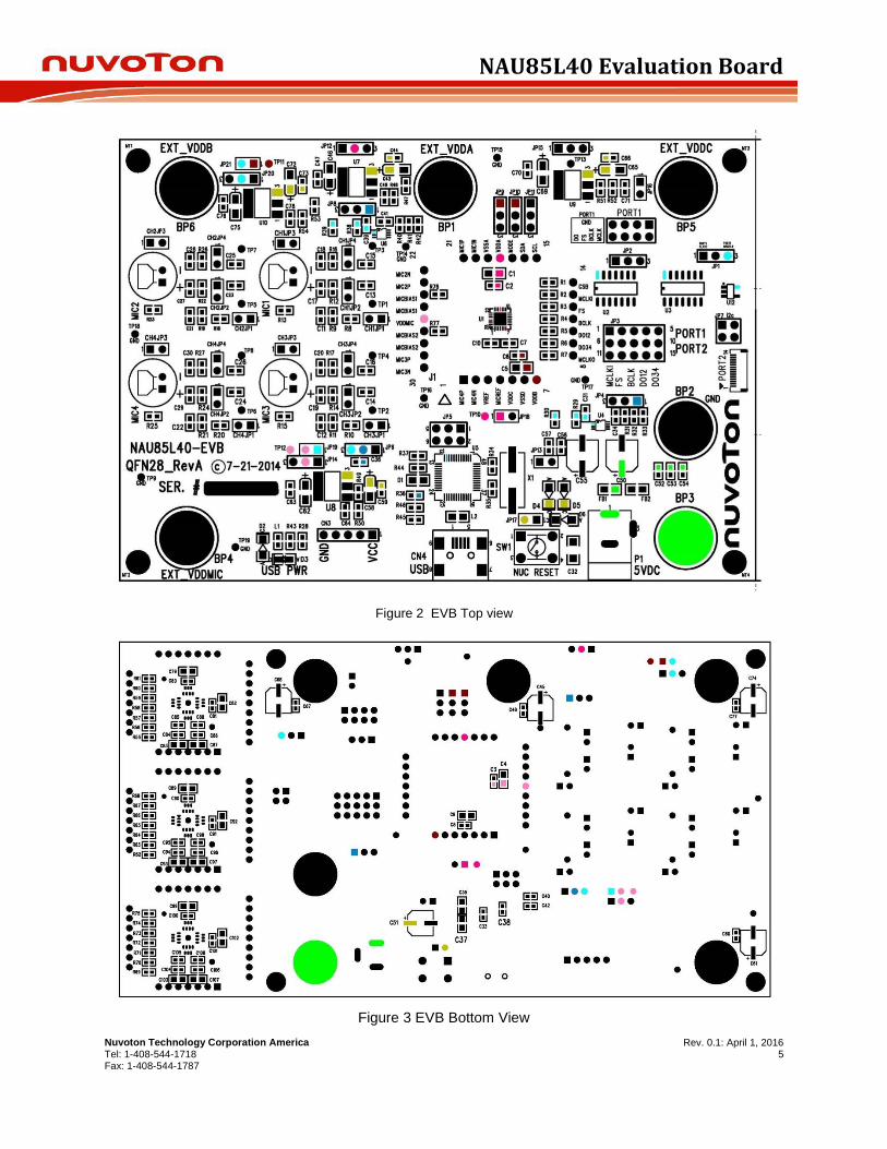
Figure 2 EVB Top view ................................................................................................................................................. 5
Figure 3 EVB Bottom View ............................................................................................................................................. 5
Figure 4: External Connectors on EVB for Power Supplies ........................................................................................... 6
Figure 5: Jumpers Locations on EVB for different Power Connections ......................................................................... 7
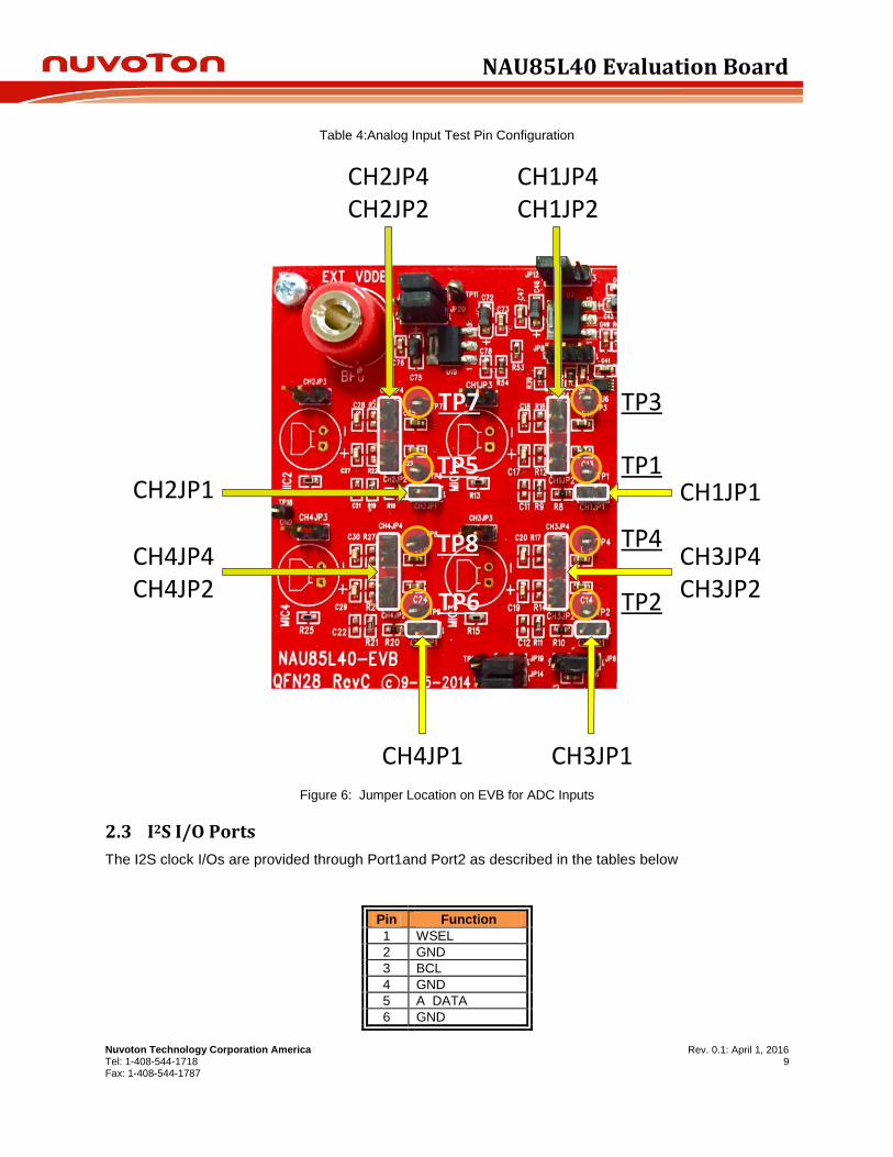
Figure 6: Jumper Location on EVB for ADC Inputs ....................................................................................................... 9
Figure 7: ADC connection with AP outputs .................................................................................................................. 12
Figure 8: AP connection for NAU85L40 ADC ............................................................................................................... 12
Figure 9: I2S Port connection forNAU85L40 ................................................................................................................ 13
Figure 10: AP Measurement Readout .......................................................................................................................... 14
Figure 11: NAU85L40 GUI Front page—Device Control .............................................................................................. 15
Figure 12: Device Control Tab dictation ....................................................................................................................... 16
Figure 13: Quick Start Tab .......................................................................................................................................... 18
Figure 14: NAU85L40 Demo GUI FLL Tab .................................................................................................................. 20
Figure 15: NAU85L40 Demo GUI Digital Audio Interface Tab ..................................................................................... 21
Figure 16: NAU85L40 Demo GUI Digital Clock Div Tab .............................................................................................. 22
Figure 17: NAU85L40 Demo GUI Digital PowerUp& Gains Tab .................................................................................. 23
NAU85L40 Evaluation Board
Nuvoton Technology Corporation America Tel: 1-408-544-1718 Fax: 1-408-544-1787
Rev. 0.1: April 1, 2016 3
Figure 18: NAU85L40 Demo GUI Digital ADC Tab ...................................................................................................... 24
Figure 19: NAU85L40 Demo GUI Digital Filters Tab .................................................................................................... 25
Figure 20: NAU85L40 Demo GUI Digital Limiter Tab ................................................................................................... 26
Figure 21: NAU85L40 Demo GUI Digital Others Tab ................................................................................................... 27
Table 1: Power Supply Voltages .................................................................................................................................... 7
Table 2: MIC Jumper Configuration ............................................................................................................................... 8
Table 3: Analog Input Configuration ............................................................................................................................... 8
Table 4:Analog Input Test Pin Configuration .................................................................................................................. 9
Table 5: I2S I/O Port2 Pin out ...................................................................................................................................... 10
Table 6: Jumper Connections Summary ...................................................................................................................... 11
NAU85L40 Evaluation Board
Nuvoton Technology Corporation America Tel: 1-408-544-1718 Fax: 1-408-544-1787
Rev. 0.1: April 1, 2016 4
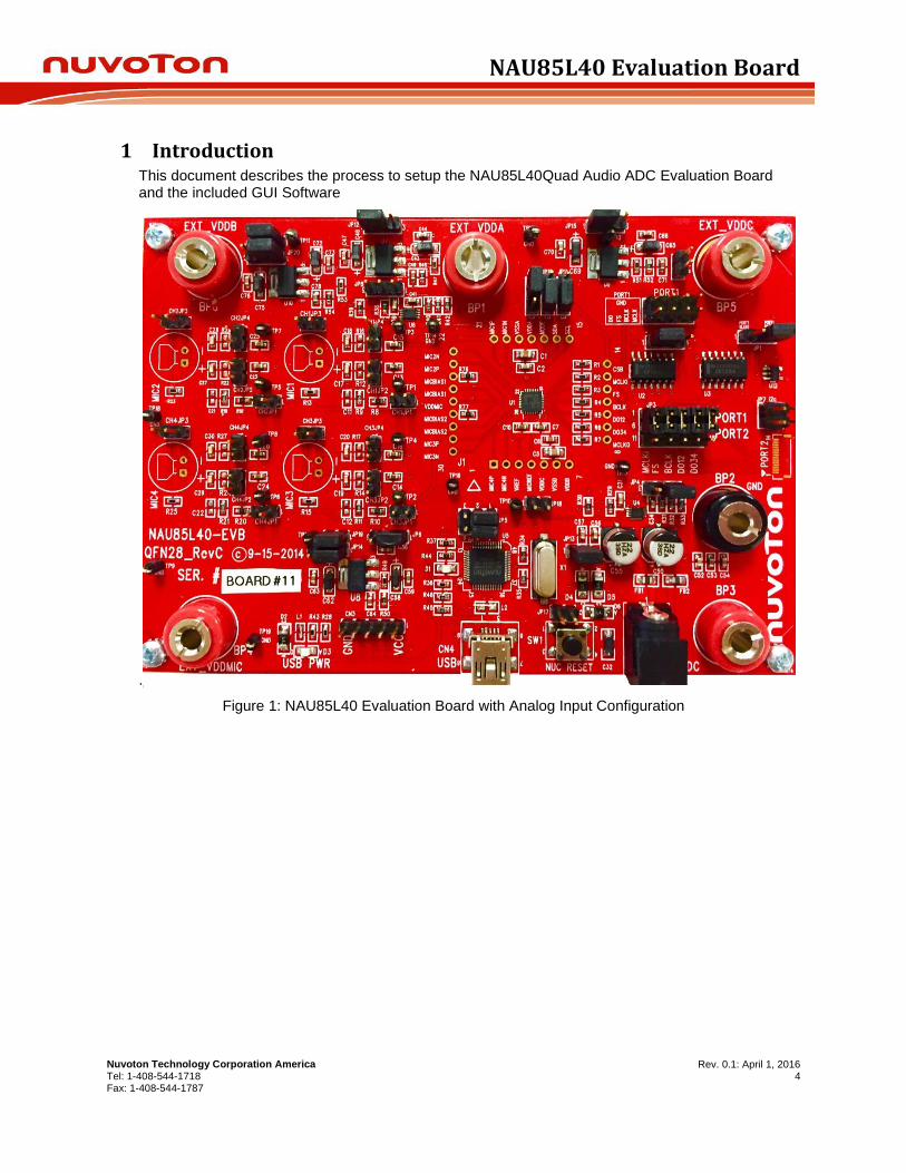
1 Introduction This document describes the process to setup the NAU85L40Quad Audio ADC Evaluation Board and the included GUI Software
.
Figure 1: NAU85L40 Evaluation Board with Analog Input Configuration
NAU85L40 Evaluation Board
Nuvoton Technology Corporation America Tel: 1-408-544-1718 Fax: 1-408-544-1787
Rev. 0.1: April 1, 2016 5
Figure 2 EVB Top view
Figure 3 EVB Bottom View
NAU85L40 Evaluation Board
Nuvoton Technology Corporation America Tel: 1-408-544-1718 Fax: 1-408-544-1787
Rev. 0.1: April 1, 2016 6
2 Setup
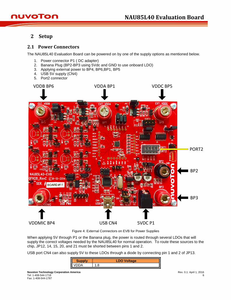
2.1 Power Connectors
The NAU85L40 Evaluation Board can be powered on by one of the supply options as mentioned below.
1. Power connector P1 ( DC adapter) 2. Banana Plug (BP2-BP3 using 5Vdc and GND to use onboard LDO) 3. Applying external power to BP4, BP6,BP1, BP5 4. USB 5V supply (CN4) 5. Port2 connector
VDDB BP6 VDDA BP1 VDDC BP5
VDDMIC BP4 USB CN4 5VDC P1
BP2
BP3
PORT2
Figure 4: External Connectors on EVB for Power Supplies
When applying 5V through P1 or the Banana plug, the power is routed through several LDOs that will supply the correct voltages needed by the NAU85L40 for normal operation. To route these sources to the chip, JP12, 14, 15, 20, and 21 must be shorted between pins 1 and 2.
USB port CN4 can also supply 5V to these LDOs through a diode by connecting pin 1 and 2 of JP13.
Supply LDO Voltage
VDDA 1.8
NAU85L40 Evaluation Board
Nuvoton Technology Corporation America Tel: 1-408-544-1718 Fax: 1-408-544-1787
Rev. 0.1: April 1, 2016 7
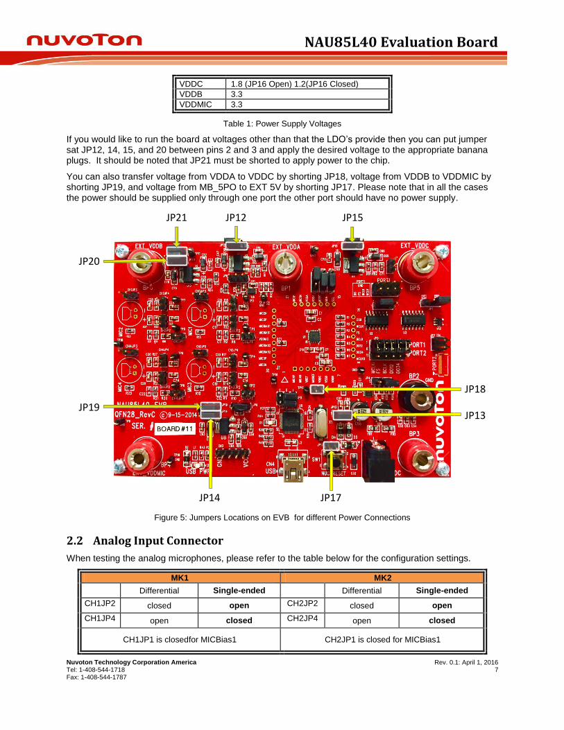
VDDC 1.8 (JP16 Open) 1.2(JP16 Closed)
VDDB 3.3
VDDMIC 3.3
Table 1: Power Supply Voltages
If you would like to run the board at voltages other than that the LDO’s provide then you can put jumper sat JP12, 14, 15, and 20 between pins 2 and 3 and apply the desired voltage to the appropriate banana plugs. It should be noted that JP21 must be shorted to apply power to the chip.
You can also transfer voltage from VDDA to VDDC by shorting JP18, voltage from VDDB to VDDMIC by shorting JP19, and voltage from MB_5PO to EXT 5V by shorting JP17. Please note that in all the cases the power should be supplied only through one port the other port should have no power supply.
JP18
JP13
JP15JP12JP21
JP20
JP19
JP14 JP17
Figure 5: Jumpers Locations on EVB for different Power Connections
2.2 Analog Input Connector
When testing the analog microphones, please refer to the table below for the configuration settings.
MK1 MK2
Differential Single-ended Differential Single-ended
CH1JP2 closed open CH2JP2 closed open
CH1JP4 open closed CH2JP4 open closed
CH1JP1 is closedfor MICBias1 CH2JP1 is closed for MICBias1
NAU85L40 Evaluation Board
Nuvoton Technology Corporation America Tel: 1-408-544-1718 Fax: 1-408-544-1787
Rev. 0.1: April 1, 2016 8
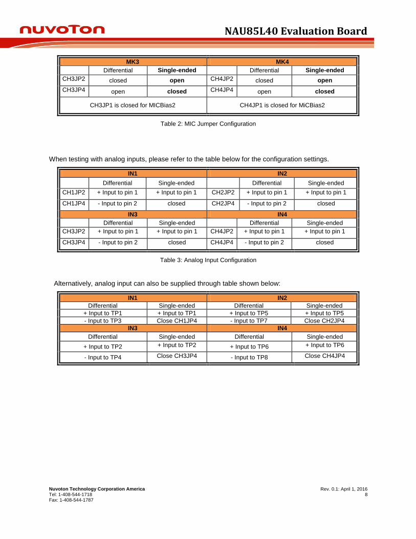
MK3 MK4
Differential Single-ended Differential Single-ended
CH3JP2 closed open CH4JP2 closed open
CH3JP4 open closed CH4JP4 open closed
CH3JP1 is closed for MICBias2 CH4JP1 is closed for MiCBias2
Table 2: MIC Jumper Configuration
When testing with analog inputs, please refer to the table below for the configuration settings.
IN1 IN2
Differential Single-ended Differential Single-ended
CH1JP2 + Input to pin 1 + Input to pin 1 CH2JP2 + Input to pin 1 + Input to pin 1
CH1JP4 - Input to pin 2 closed CH2JP4 - Input to pin 2 closed
IN3 IN4
Differential Single-ended Differential Single-ended
CH3JP2 + Input to pin 1 + Input to pin 1 CH4JP2 + Input to pin 1 + Input to pin 1
CH3JP4 - Input to pin 2 closed CH4JP4 - Input to pin 2 closed
Table 3: Analog Input Configuration
Alternatively, analog input can also be supplied through table shown below:
IN1 IN2
Differential Single-ended Differential Single-ended
+ Input to TP1 + Input to TP1 + Input to TP5 + Input to TP5
- Input to TP3 Close CH1JP4 - Input to TP7 Close CH2JP4
IN3 IN4
Differential Single-ended Differential Single-ended
+ Input to TP2 + Input to TP2 + Input to TP6 + Input to TP6
- Input to TP4 Close CH3JP4 - Input to TP8 Close CH4JP4
NAU85L40 Evaluation Board
Nuvoton Technology Corporation America Tel: 1-408-544-1718 Fax: 1-408-544-1787
Rev. 0.1: April 1, 2016 9
Table 4:Analog Input Test Pin Configuration
CH3JP4CH3JP2
CH1JP1
CH3JP1CH4JP1
CH4JP4CH4JP2
CH2JP1
CH2JP4CH2JP2
CH1JP4CH1JP2
TP3
TP1
TP4
TP2
TP7
TP5
TP8
TP6
Figure 6: Jumper Location on EVB for ADC Inputs
2.3 I2S I/O Ports
The I2S clock I/Os are provided through Port1and Port2 as described in the tables below
Pin Function
1 WSEL
2 GND
3 BCL
4 GND
5 A DATA
6 GND
NAU85L40 Evaluation Board
Nuvoton Technology Corporation America Tel: 1-408-544-1718 Fax: 1-408-544-1787
Rev. 0.1: April 1, 2016 10
Table 4: I2S I/O Port1 Pin Out
Pin Function
1 GND
2 Master Clock
3 GND
4 Bit Clock
5 GND
6 Frame Clock
7 GND
8 Data Out
Table 5: I2S I/O Port2 Pin Out
To select port1 connect pins 1-6, 2-7, 3-8, 4-9, and 5-10 of JP3.Else,to select port2 short pins 6-11, 7-12, 8-13, 9-14, and 10-15 of JP3.Port1 can be used for measurement with analyzer.
If AP is configured as master of I2S bus then JP1 1-2 jumper need to be used. In case AP is configured as slave use JP1 2-3.
You can select two possible set of Digital Output through JP2. If pins 2 and 3 of JP2 are shorted the digital output of Channel 1 and 2(ADC DO12 pin 10 on DUT) is selected. And if pins 1 and 2 are shorted the digital output of Channel 3 and 4(ADC DO34 pin 9 on DUT) is selected.
For I2C communication connect pins 1 and 2 of JP4 and JP5, please leave other pins of JP5 open for RevA board. Short pins 1 and 2 of JP6 if you are using USB supply. Else if you are using VDDB supply Verify that the VDDB voltage level is at 3.3V and connect pins 2 and 3 of JP6. You can connect pins 1 and 2 of JP9 to enable Mode pin for 2-wire Read/Write operation. The Device Address of the NAU85L04 is either 0x1C(CSB=0) or 0x1D (CSB=1).
2.4 Jumper setting summary
Table 6 below shows all the jumper connections and its corresponding functions:
7 B DATA
8 GND
9 MCLK
10 GND
11 I2C_SCL
12 I2C_SDA
13 GND
14 5 PO
Jumper Number
Pins Connected
Function Comments
JP12 1 and 2 VDDA from LDO
2 and 3 External VDDA
JP14 1 and 2 VDDMIC from LDO
2 and 3 External VDDMIC
JP15 1 and 2 VDDC from LDO
2 and 3 External VDDC
JP20 1 and 2 VDDB from LDO Use along with JP21
NAU85L40 Evaluation Board
Nuvoton Technology Corporation America Tel: 1-408-544-1718 Fax: 1-408-544-1787
Rev. 0.1: April 1, 2016 11
Table 6: Jumper Connections Summary
2.5 PCB Setting
2 and 3 External VDDB
JP21 1 and 2 VDDB from LDO Should be shorted to supply power to the chip
JP13 1 and 2 USB 5V to EXT5V Should be used only if USB power supply is used to power the chip.
JP18 1 and 2 VDDA shorted to VDDC
JP19 1 and 2 VDDB shorted to VDDMIC
JP17 1 and 2 MB_5PO shorted to EXT 5V
CH1JP2 1 and 2 MIC1 Differential
CH1JP4 1 and 2 MIC1 Single Ended
CH1JP1 1 and 2 Supplies MICBias1 to MIC1
CH2JP2 1 and 2 MIC2 Differential
CH2JP4 1 and 2 MIC2 Single Ended
CH2JP1 1 and 2 Supplies MICBias1 to MIC2
CH3JP2 1 and 2 MIC3 Differential
CH3JP4 1 and 2 MIC3 Single Ended
CH3JP1 1 and 2 Supplies MICBias2 to MIC3
CH4JP2 1 and 2 MIC4 Differential
CH4JP4 1 and 2 MIC4 Single Ended
CH4JP1 1 and 2 Supplies MICBias2 to MIC4
JP3
1 and 6
PORT1 in use
2 and 7
3 and 8
4 and 9
5 and 10
6 and 11
PORT2 in use
7 and 12
8 and 13
9 and 14
10 and 15
JP1 2 and 3 Set AP as MASTER
1 and 2 Set AP as SLAVE
JP2 2 and 3 DO of CH1 and 2 selected ADC DO12 pin 10 on DUT
1 and 2 DO of CH3 and 4 selected ADC DO34 pin 9 on DUT
JP4 1 and 2 I2C Comm Enable U4.
JP5 1 and 2 I2C Comm
JP6 1 and 2
I2C Comm When using USB supply
2 and 3 When using VDDB
JP9 1 and 2 MODE Pin Hi
JP10 1 and 2 CSB HI 0x1D address
2 and 3 CSB LO 0x1C address
JP11 2 and 3 Set CSB as I2C address selection pin.
NAU85L40 Evaluation Board
Nuvoton Technology Corporation America Tel: 1-408-544-1718 Fax: 1-408-544-1787
Rev. 0.1: April 1, 2016 12
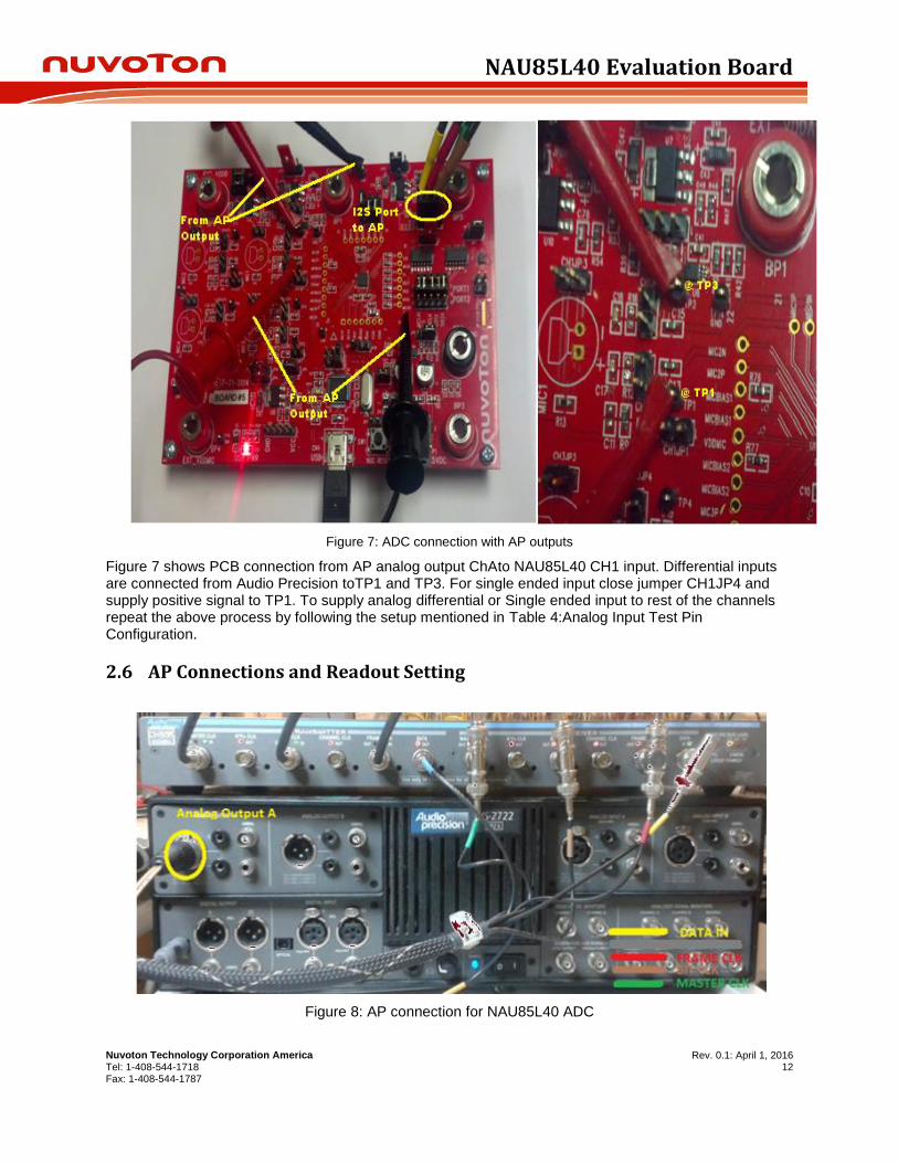
Figure 7: ADC connection with AP outputs
Figure 7 shows PCB connection from AP analog output ChAto NAU85L40 CH1 input. Differential inputs are connected from Audio Precision toTP1 and TP3. For single ended input close jumper CH1JP4 and supply positive signal to TP1. To supply analog differential or Single ended input to rest of the channels repeat the above process by following the setup mentioned in Table 4:Analog Input Test Pin Configuration.
2.6 AP Connections and Readout Setting
Figure 8: AP connection for NAU85L40 ADC
NAU85L40 Evaluation Board
Nuvoton Technology Corporation America Tel: 1-408-544-1718 Fax: 1-408-544-1787
Rev. 0.1: April 1, 2016 13
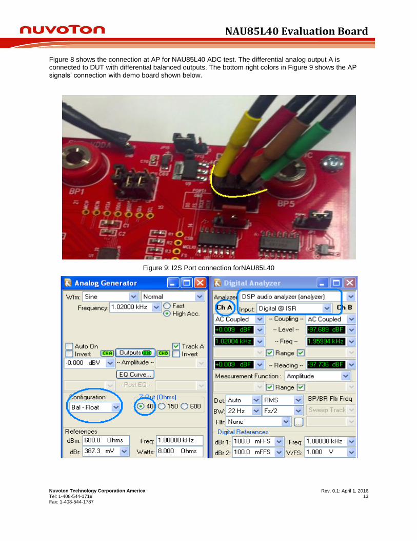
Figure 8 shows the connection at AP for NAU85L40 ADC test. The differential analog output A is connected to DUT with differential balanced outputs. The bottom right colors in Figure 9 shows the AP signals’ connection with demo board shown below.
Figure 9: I2S Port connection forNAU85L40
NAU85L40 Evaluation Board
Nuvoton Technology Corporation America Tel: 1-408-544-1718 Fax: 1-408-544-1787
Rev. 0.1: April 1, 2016 14
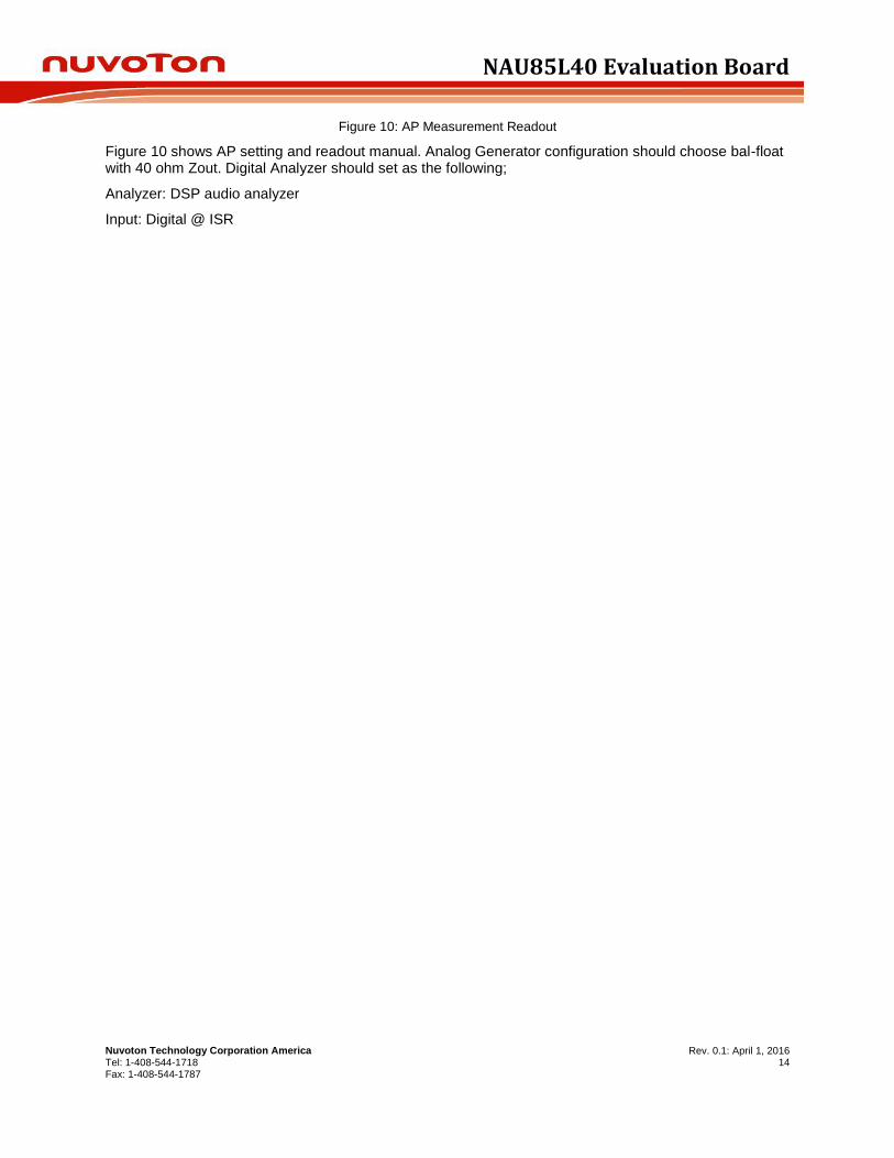
Figure 10: AP Measurement Readout
Figure 10 shows AP setting and readout manual. Analog Generator configuration should choose bal-float with 40 ohm Zout. Digital Analyzer should set as the following;
Analyzer: DSP audio analyzer
Input: Digital @ ISR
NAU85L40 Evaluation Board
Nuvoton Technology Corporation America Tel: 1-408-544-1718 Fax: 1-408-544-1787
Rev. 0.1: April 1, 2016 15
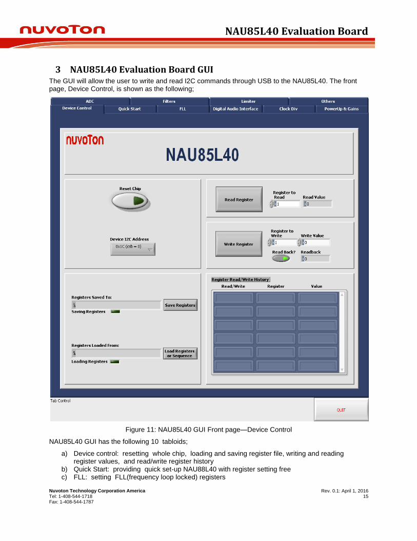
3 NAU85L40 Evaluation Board GUI The GUI will allow the user to write and read I2C commands through USB to the NAU85L40. The front page, Device Control, is shown as the following;
Figure 11: NAU85L40 GUI Front page—Device Control
NAU85L40 GUI has the following 10 tabloids;
a) Device control: resetting whole chip, loading and saving register file, writing and reading register values, and read/write register history
b) Quick Start: providing quick set-up NAU88L40 with register setting free c) FLL: setting FLL(frequency loop locked) registers
NAU85L40 Evaluation Board
Nuvoton Technology Corporation America Tel: 1-408-544-1718 Fax: 1-408-544-1787
Rev. 0.1: April 1, 2016 16
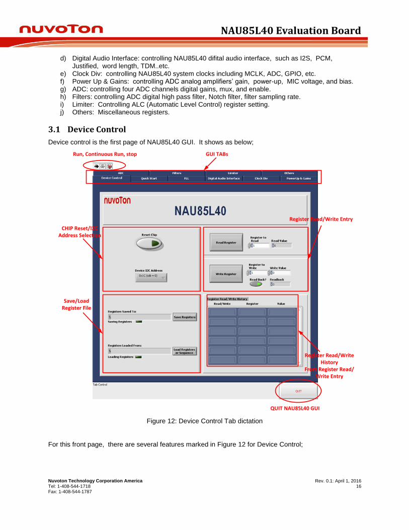
d) Digital Audio Interface: controlling NAU85L40 difital audio interface, such as I2S, PCM, Justified, word length, TDM..etc.
e) Clock Div: controlling NAU85L40 system clocks including MCLK, ADC, GPIO, etc. f) Power Up & Gains: controlling ADC analog amplifiers’ gain, power-up, MIC voltage, and bias. g) ADC: controlling four ADC channels digital gains, mux, and enable. h) Filters: controlling ADC digital high pass filter, Notch filter, filter sampling rate. i) Limiter: Controlling ALC (Automatic Level Control) register setting. j) Others: Miscellaneous registers.
3.1 Device Control
Device control is the first page of NAU85L40 GUI. It shows as below;
Run, Continuous Run, stop GUI TABs
CHIP Reset/I2C Address Selection
QUIT NAU85L40 GUI
Register Read/Write Entry
Register Read/Write History
From Register Read/Write Entry
Save/LoadRegister File
Figure 12: Device Control Tab dictation
For this front page, there are several features marked in Figure 12 for Device Control;
NAU85L40 Evaluation Board
Nuvoton Technology Corporation America Tel: 1-408-544-1718 Fax: 1-408-544-1787
Rev. 0.1: April 1, 2016 17
a) RUN, Continuous Run, STOP: are buttons for run, continuous run, and
stop command for Nau85L40 GUI. When click the white arrow, , GUI starts to run.
will change to . During GUI running, , click to stop GUI.
b) GUI Tabs; The summary of all NAU85L40 Tabs shows on top edge. Clicking specific tab, GUI will enter the tab for further application. As shown and marked in Figure 12, currently there are ten tabs available.
c) CHIP Reset/I2C Address Chip reset: reset button will clean up all current register settings saving in GUI, and I2C address selection is used to select a right I2C address for GUI.
d) Register Read/Write Entry: register settings tab allows the user to write to and read from a single register. When writing a register, you can choose whether or not to have the GUI automatically read the register after every write by using the “Read back?”
,button. Using this button ensures that the register was written correctly.
e) Save/Load Register file: button will save all registers to or load a set of registers to or
from a text file of your choice. To load a file, click button, a directory path window will show up for you to select register file. To save verified register settins,
clicking and allocate the register settings to target directory f) Register Read/Write History: the table will show the last 6 entry from read/write register
setting. g) QUIT: Selecting “Quit” button to quit NAU85L40 GUI.
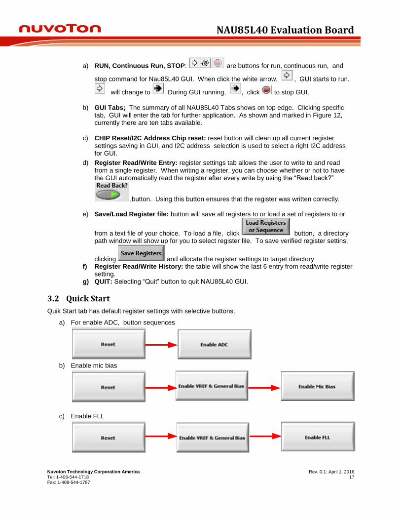
3.2 Quick Start
Quik Start tab has default register settings with selective buttons.
a) For enable ADC, button sequences
b) Enable mic bias
c) Enable FLL
NAU85L40 Evaluation Board
Nuvoton Technology Corporation America Tel: 1-408-544-1718 Fax: 1-408-544-1787
Rev. 0.1: April 1, 2016 18
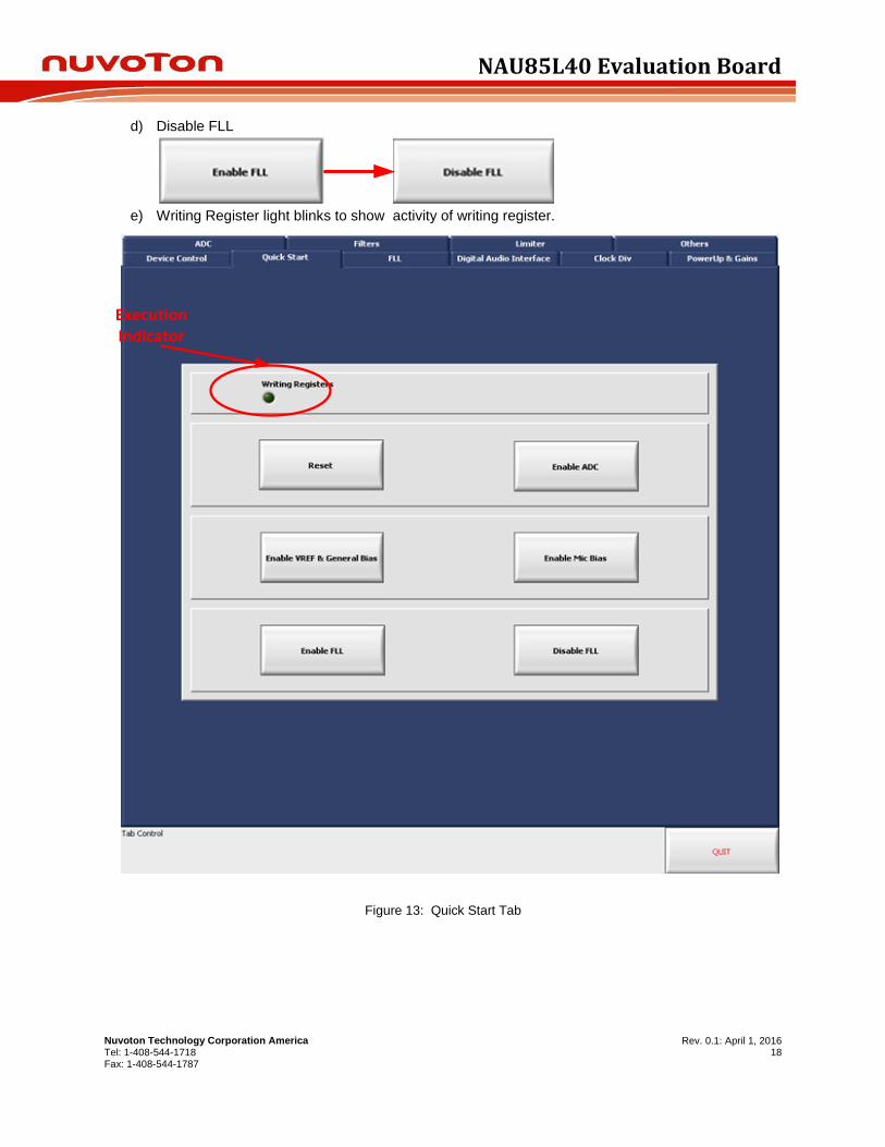
d) Disable FLL
e) Writing Register light blinks to show activity of writing register.
ExecutionIndicator
Figure 13: Quick Start Tab
NAU85L40 Evaluation Board
Nuvoton Technology Corporation America Tel: 1-408-544-1718 Fax: 1-408-544-1787
Rev. 0.1: April 1, 2016 19
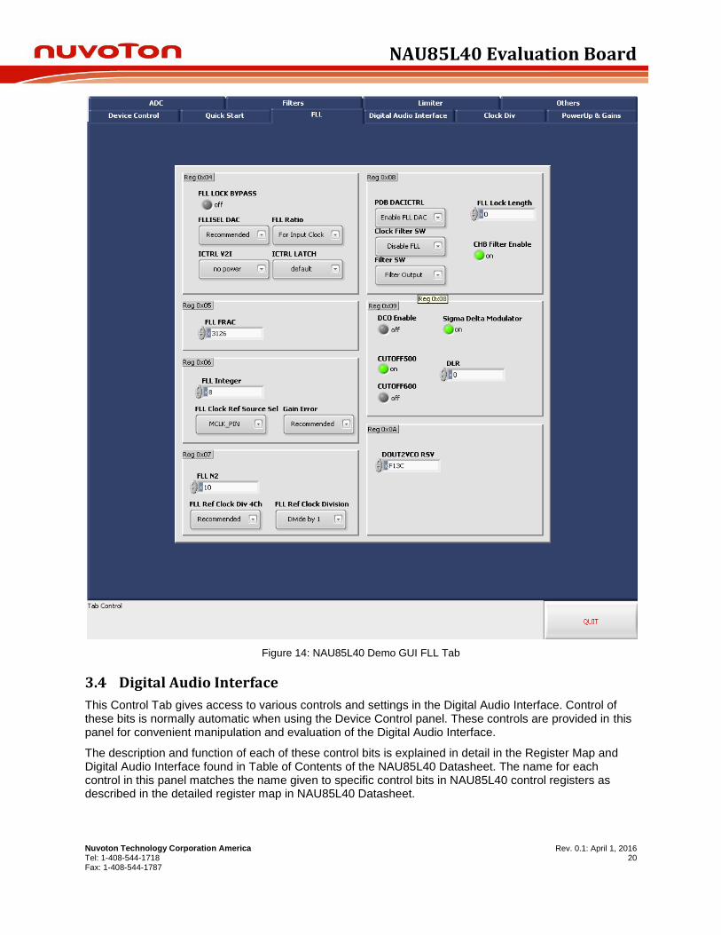
3.3 FLL
The integrated FLL can be used to generate a master system clock, MCLK, from MCLKl, BCLK or FS as a reference. Because of the FLL’s tolerance of jitter, it may be used to generate a stable MCLK from less stable input clock sources or it can be used to generate a free-running clock in the absence of an external reference clock source.
This Control Tab gives access to various controls and settings in the FLL block. Control of these bits is normally automatic when using the Device Control panel. These controls are provided in this panel for convenient manipulation and evaluation of the FLL section features.
The description and function of each of these control bits is explained in detail in the Register Map and FLL found in Table of Contents of the NAU85L40 Datasheet. The name for each control in this panel matches the name given to specific control bits in NAU85L40 control registers as described in the detailed register map in NAU85L40 Datasheet.
NAU85L40 Evaluation Board
Nuvoton Technology Corporation America Tel: 1-408-544-1718 Fax: 1-408-544-1787
Rev. 0.1: April 1, 2016 20
Figure 14: NAU85L40 Demo GUI FLL Tab
3.4 Digital Audio Interface
This Control Tab gives access to various controls and settings in the Digital Audio Interface. Control of these bits is normally automatic when using the Device Control panel. These controls are provided in this panel for convenient manipulation and evaluation of the Digital Audio Interface.
The description and function of each of these control bits is explained in detail in the Register Map and Digital Audio Interface found in Table of Contents of the NAU85L40 Datasheet. The name for each control in this panel matches the name given to specific control bits in NAU85L40 control registers as described in the detailed register map in NAU85L40 Datasheet.
NAU85L40 Evaluation Board
Nuvoton Technology Corporation America Tel: 1-408-544-1718 Fax: 1-408-544-1787
Rev. 0.1: April 1, 2016 21
Figure 15: NAU85L40 Demo GUI Digital Audio Interface Tab
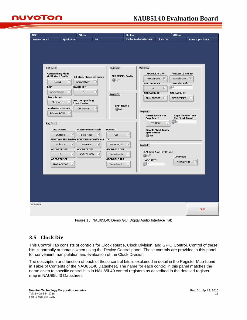
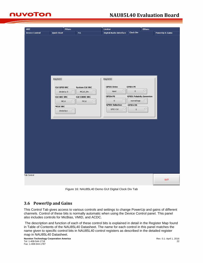
3.5 Clock Div
This Control Tab consists of controls for Clock source, Clock Division, and GPIO Control. Control of these bits is normally automatic when using the Device Control panel. These controls are provided in this panel for convenient manipulation and evaluation of the Clock Division.
The description and function of each of these control bits is explained in detail in the Register Map found in Table of Contents of the NAU85L40 Datasheet. The name for each control in this panel matches the name given to specific control bits in NAU85L40 control registers as described in the detailed register map in NAU85L40 Datasheet.
NAU85L40 Evaluation Board
Nuvoton Technology Corporation America Tel: 1-408-544-1718 Fax: 1-408-544-1787
Rev. 0.1: April 1, 2016 22
Figure 16: NAU85L40 Demo GUI Digital Clock Div Tab
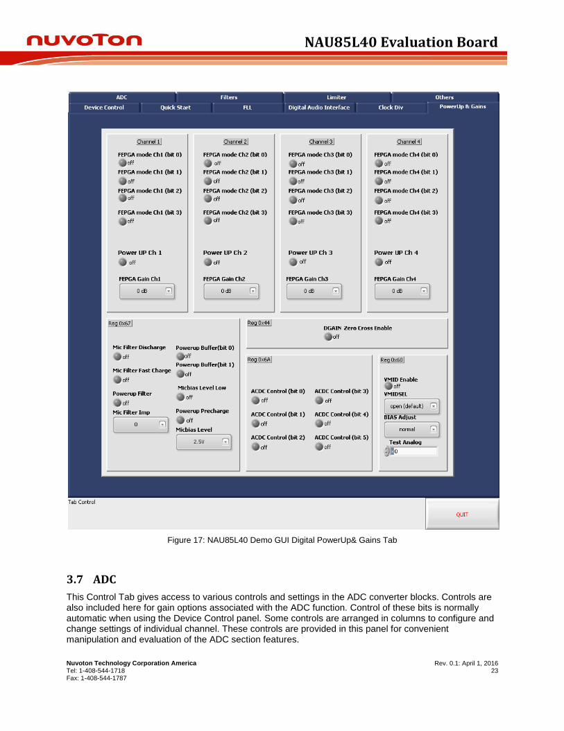
3.6 PowerUp and Gains
This Control Tab gives access to various controls and settings to change PowerUp and gains of different channels. Control of these bits is normally automatic when using the Device Control panel. This panel also includes controls for MicBias, VMID, and ACDC.
The description and function of each of these control bits is explained in detail in the Register Map found in Table of Contents of the NAU85L40 Datasheet. The name for each control in this panel matches the name given to specific control bits in NAU85L40 control registers as described in the detailed register map in NAU85L40 Datasheet.
NAU85L40 Evaluation Board
Nuvoton Technology Corporation America Tel: 1-408-544-1718 Fax: 1-408-544-1787
Rev. 0.1: April 1, 2016 23
Figure 17: NAU85L40 Demo GUI Digital PowerUp& Gains Tab
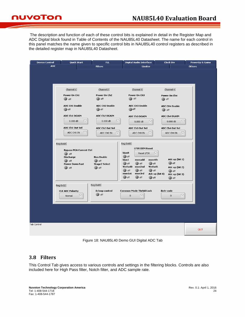
3.7 ADC
This Control Tab gives access to various controls and settings in the ADC converter blocks. Controls are also included here for gain options associated with the ADC function. Control of these bits is normally automatic when using the Device Control panel. Some controls are arranged in columns to configure and change settings of individual channel. These controls are provided in this panel for convenient manipulation and evaluation of the ADC section features.
NAU85L40 Evaluation Board
Nuvoton Technology Corporation America Tel: 1-408-544-1718 Fax: 1-408-544-1787
Rev. 0.1: April 1, 2016 24
The description and function of each of these control bits is explained in detail in the Register Map and ADC Digital block found in Table of Contents of the NAU85L40 Datasheet. The name for each control in this panel matches the name given to specific control bits in NAU85L40 control registers as described in the detailed register map in NAU85L40 Datasheet.
Figure 18: NAU85L40 Demo GUI Digital ADC Tab
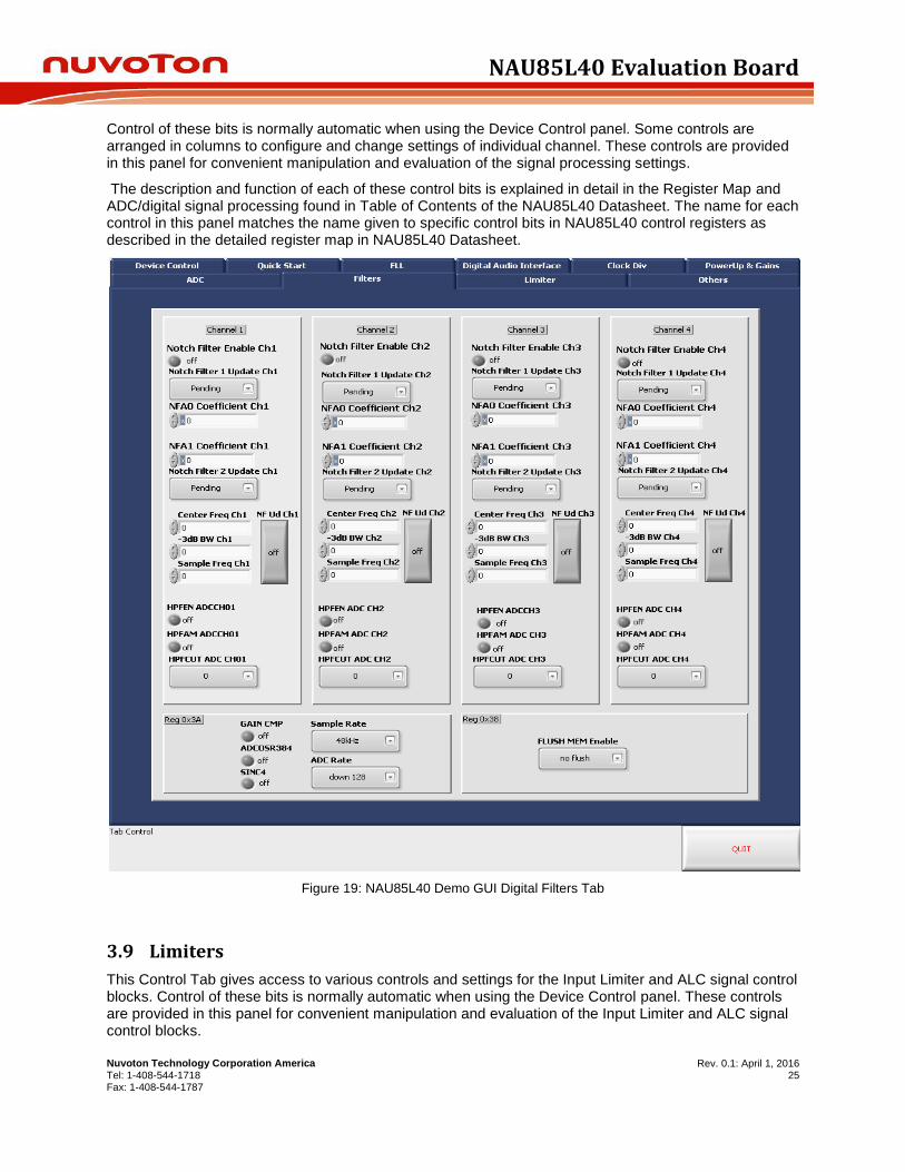
3.8 Filters
This Control Tab gives access to various controls and settings in the filtering blocks. Controls are also included here for High Pass filter, Notch filter, and ADC sample rate.
NAU85L40 Evaluation Board
Nuvoton Technology Corporation America Tel: 1-408-544-1718 Fax: 1-408-544-1787
Rev. 0.1: April 1, 2016 25
Control of these bits is normally automatic when using the Device Control panel. Some controls are arranged in columns to configure and change settings of individual channel. These controls are provided in this panel for convenient manipulation and evaluation of the signal processing settings.
The description and function of each of these control bits is explained in detail in the Register Map and ADC/digital signal processing found in Table of Contents of the NAU85L40 Datasheet. The name for each control in this panel matches the name given to specific control bits in NAU85L40 control registers as described in the detailed register map in NAU85L40 Datasheet.
Figure 19: NAU85L40 Demo GUI Digital Filters Tab
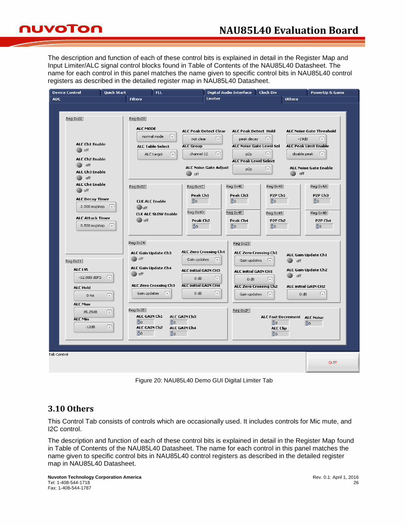
3.9 Limiters
This Control Tab gives access to various controls and settings for the Input Limiter and ALC signal control blocks. Control of these bits is normally automatic when using the Device Control panel. These controls are provided in this panel for convenient manipulation and evaluation of the Input Limiter and ALC signal control blocks.
NAU85L40 Evaluation Board
Nuvoton Technology Corporation America Tel: 1-408-544-1718 Fax: 1-408-544-1787
Rev. 0.1: April 1, 2016 26
The description and function of each of these control bits is explained in detail in the Register Map and Input Limiter/ALC signal control blocks found in Table of Contents of the NAU85L40 Datasheet. The name for each control in this panel matches the name given to specific control bits in NAU85L40 control registers as described in the detailed register map in NAU85L40 Datasheet.
Figure 20: NAU85L40 Demo GUI Digital Limiter Tab
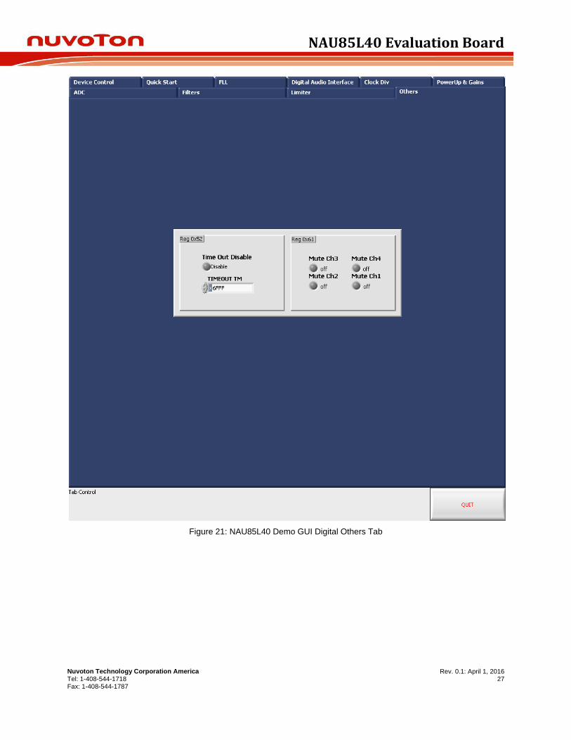
3.10 Others
This Control Tab consists of controls which are occasionally used. It includes controls for Mic mute, and I2C control.
The description and function of each of these control bits is explained in detail in the Register Map found in Table of Contents of the NAU85L40 Datasheet. The name for each control in this panel matches the name given to specific control bits in NAU85L40 control registers as described in the detailed register map in NAU85L40 Datasheet.
NAU85L40 Evaluation Board
Nuvoton Technology Corporation America Tel: 1-408-544-1718 Fax: 1-408-544-1787
Rev. 0.1: April 1, 2016 27
Figure 21: NAU85L40 Demo GUI Digital Others Tab
NAU85L40 Evaluation Board
Nuvoton Technology Corporation America Tel: 1-408-544-1718 Fax: 1-408-544-1787
Rev. 0.1: April 1, 2016 28
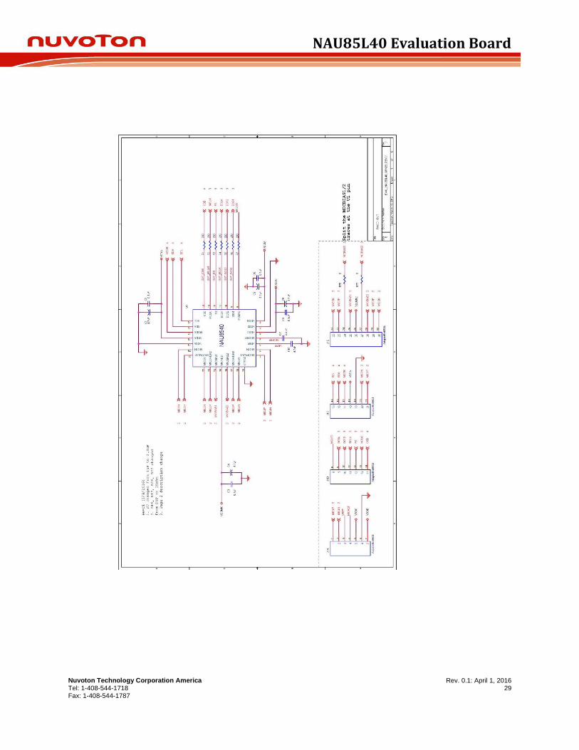
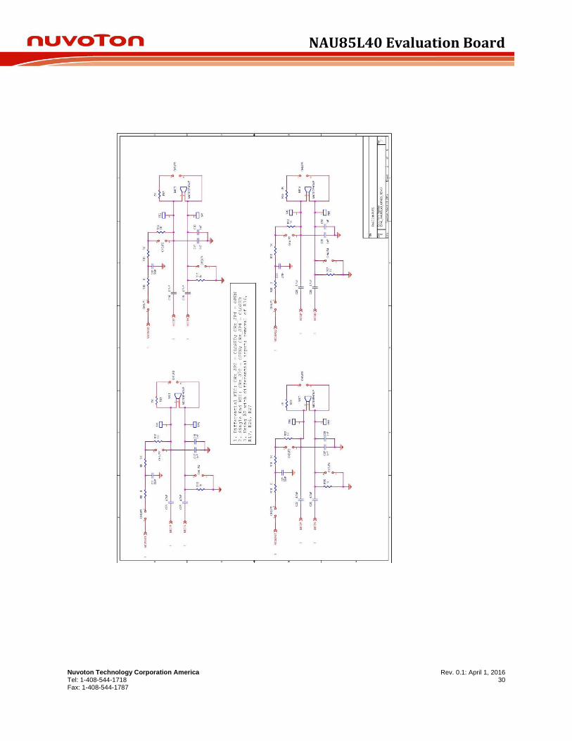
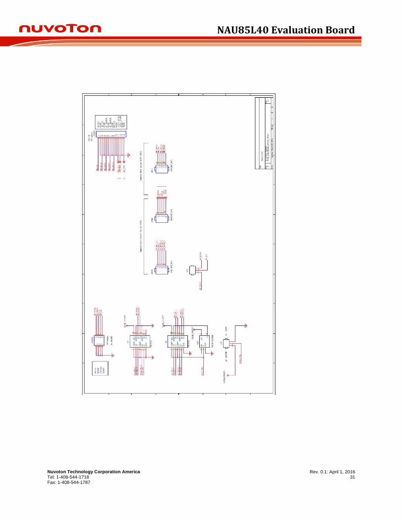
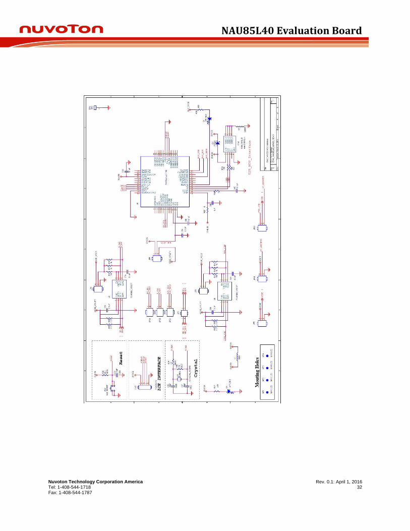
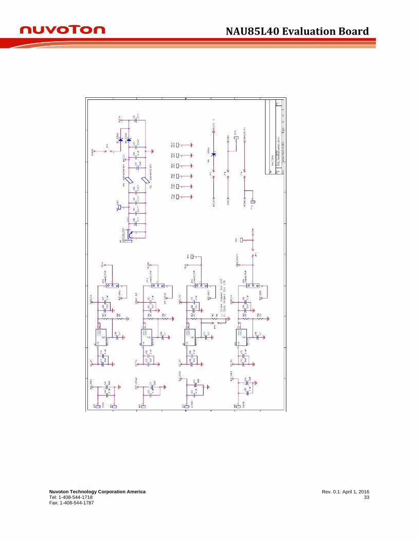
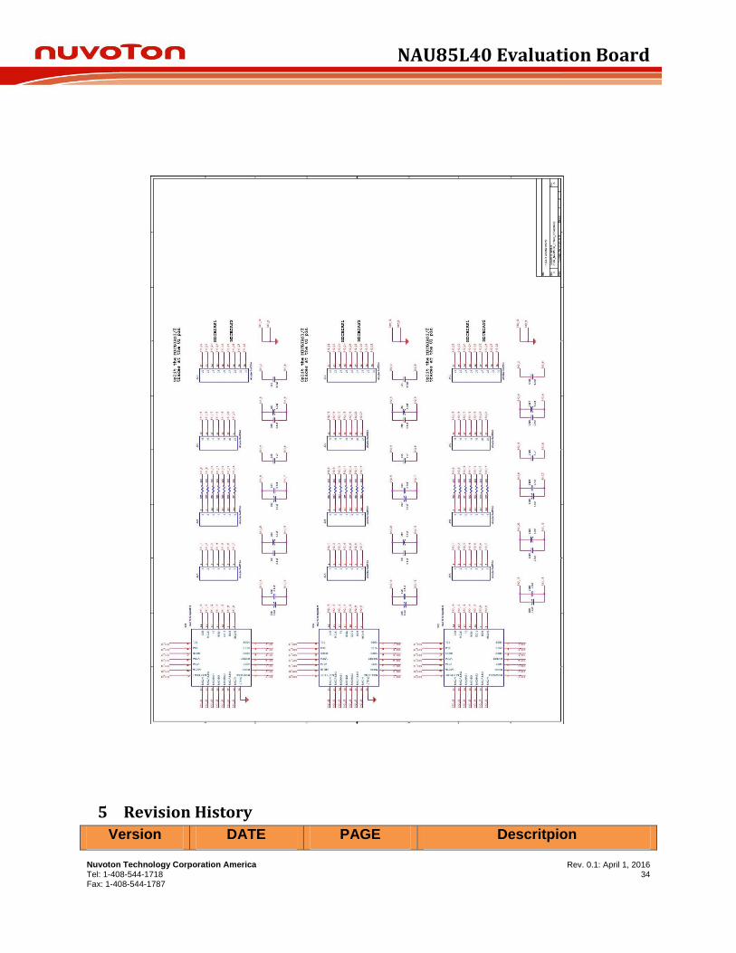
4 NAU85L40 Evaluation Board Schematic
NAU85L40 Evaluation Board
Nuvoton Technology Corporation America Tel: 1-408-544-1718 Fax: 1-408-544-1787
Rev. 0.1: April 1, 2016 29
NAU85L40 Evaluation Board
Nuvoton Technology Corporation America Tel: 1-408-544-1718 Fax: 1-408-544-1787
Rev. 0.1: April 1, 2016 30
NAU85L40 Evaluation Board
Nuvoton Technology Corporation America Tel: 1-408-544-1718 Fax: 1-408-544-1787
Rev. 0.1: April 1, 2016 31
NAU85L40 Evaluation Board
Nuvoton Technology Corporation America Tel: 1-408-544-1718 Fax: 1-408-544-1787
Rev. 0.1: April 1, 2016 32
NAU85L40 Evaluation Board
Nuvoton Technology Corporation America Tel: 1-408-544-1718 Fax: 1-408-544-1787
Rev. 0.1: April 1, 2016 33
NAU85L40 Evaluation Board
Nuvoton Technology Corporation America Tel: 1-408-544-1718 Fax: 1-408-544-1787
Rev. 0.1: April 1, 2016 34
5 Revision History
Version DATE PAGE Descritpion
NAU85L40 Evaluation Board
Nuvoton Technology Corporation America Tel: 1-408-544-1718 Fax: 1-408-544-1787
Rev. 0.1: April 1, 2016 35
0.1 April 1, 2015 28-33 Updated new schematic


![AK7734 Evaluation Board Rev - AKM Evaluation Board Rev.1 AKD7734-A [AKD7734-A] 2011/07 - 2 - Evaluation Board Diagram Board Diagram +12V-12V](https://img.pdfslide.us/doc/110x75/5c03e45309d3f203258d6861/ak7734-evaluation-board-rev-akm-evaluation-board-rev1-akd7734-a-akd7734-a-201107.jpg)