Embed Size (px)
Citation preview
Charles M. LieberHarvard University
Nanowires: A Platform for Nanoscience & Nanotechnology
http://cmliris.harvard.edu
Outline of PresentationWhy Nanowires Synthesis of Functional NanowiresNanoelectronic-Biology InterfaceConclusions & Future
Why Nanowires?
Central importance of nanoscale wires in integrated nanosystemsFundamental scientific questions in 1-dimensional systemsSynthetic challenge of controlling structure and composition on many length scalesNew/novel materials can make revolutionary vs. evolutionary changes in science and technology!
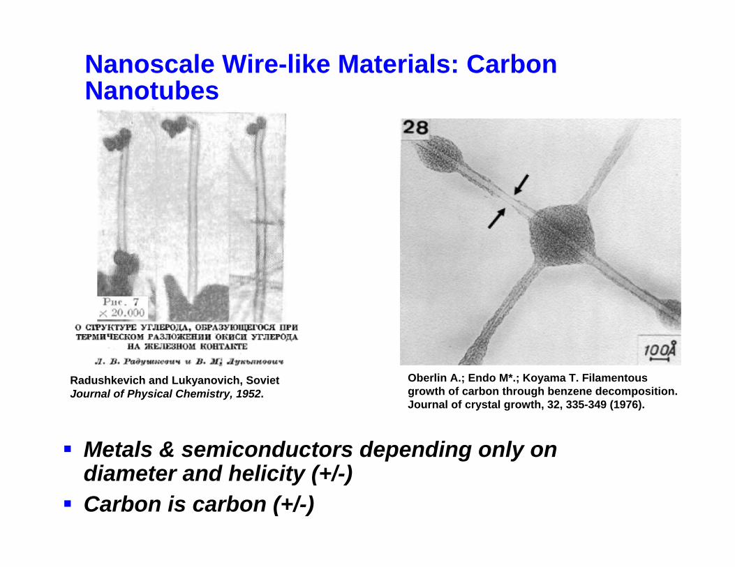
Nanoscale Wire-like Materials: Carbon Nanotubes
Oberlin A.; Endo M*.; Koyama T. Filamentous growth of carbon through benzene decomposition. Journal of crystal growth, 32, 335-349 (1976).
Radushkevich and Lukyanovich, Soviet Journal of Physical Chemistry, 1952.
Metals & semiconductors depending only on diameter and helicity (+/-)Carbon is carbon (+/-)
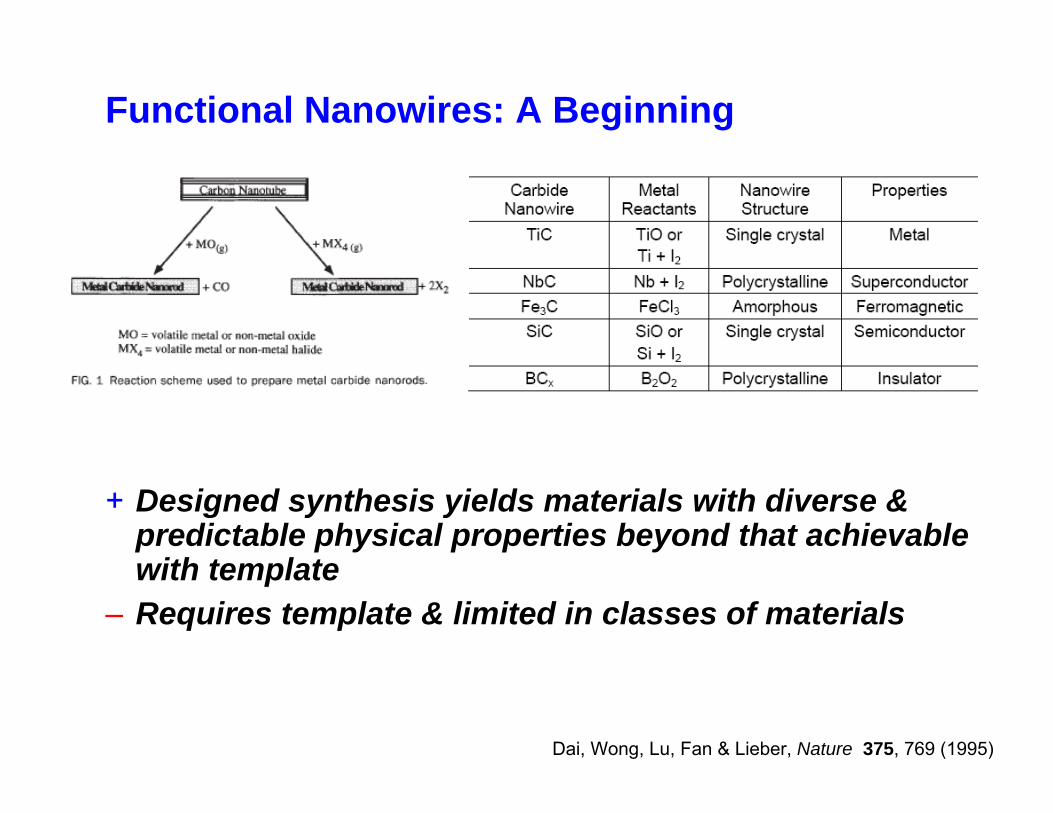
Functional Nanowires: A Beginning
Dai, Wong, Lu, Fan & Lieber, Nature 375, 769 (1995)
+ Designed synthesis yields materials with diverse & predictable physical properties beyond that achievable with template
– Requires template & limited in classes of materials
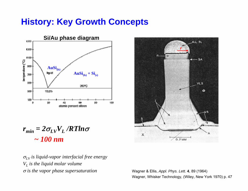
Si/Au phase diagram
Wagner, Whisker Technology, (Wiley, New York 1970) p. 47
AuSi(ls) + Si(s)
History: Key Growth Concepts
AuSi(ls)
r
rmin = 2σLVVL /RTlnσ~ 100 nm
σLV is liquid-vapor interfacial free energyVL is the liquid molar volumeσ is the vapor phase supersaturation Wagner & Ellis, Appl. Phys. Lett. 4, 89 (1964)
Nanowires: A General & Predictable Approach
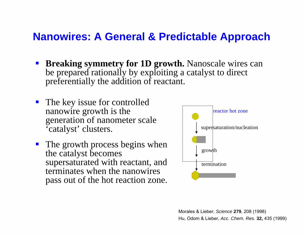
Breaking symmetry for 1D growth. Nanoscale wires can be prepared rationally by exploiting a catalyst to direct preferentially the addition of reactant.
supersaturation/nucleation
growth
termination
reactor hot zoneThe key issue for controlled nanowire growth is the generation of nanometer scale ‘catalyst’ clusters.
The growth process begins when the catalyst becomes supersaturated with reactant, and terminates when the nanowires pass out of the hot reaction zone.
Morales & Lieber, Science 279, 208 (1998)Hu, Odom & Lieber, Acc. Chem. Res. 32, 435 (1999)
Nanocluster-Catalyzed Nanowire Growth: An Early Summary
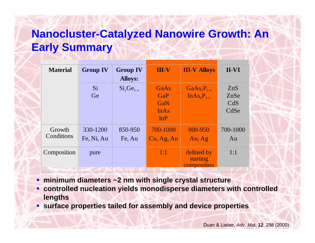
minimum diameters ~2 nm with single crystal structurecontrolled nucleation yields monodisperse diameters with controlled lengthssurface properties tailed for assembly and device properties
Material Group IV Group IVAlloys:
III-V III-V Alloys II-VI
SiGe
SixGe1-x GaAsGaPGaNInAsInP
GaAsxP1-x
InAsxP1-x
ZnSZnSeCdS
CdSe
GrowthConditions
330-1200Fe, Ni, Au
850-950Fe, Au
700-1000Cu, Ag, Au
800-950Au, Ag
700-1000Au
Composition pure 1:1 defined bystarting
composition
1:1
Duan & Lieber, Adv. Mat. 12, 298 (2000)
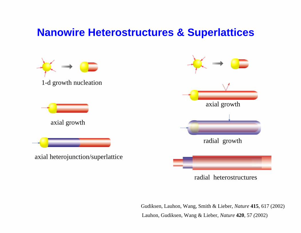
Nanowire Heterostructures & Superlattices
1-d growth nucleation
axial growth
axial heterojunction/superlattice
Gudiksen, Lauhon, Wang, Smith & Lieber, Nature 415, 617 (2002)
Lauhon, Gudiksen, Wang & Lieber, Nature 420, 57 (2002)
radial growth
axial growth
radial heterostructures
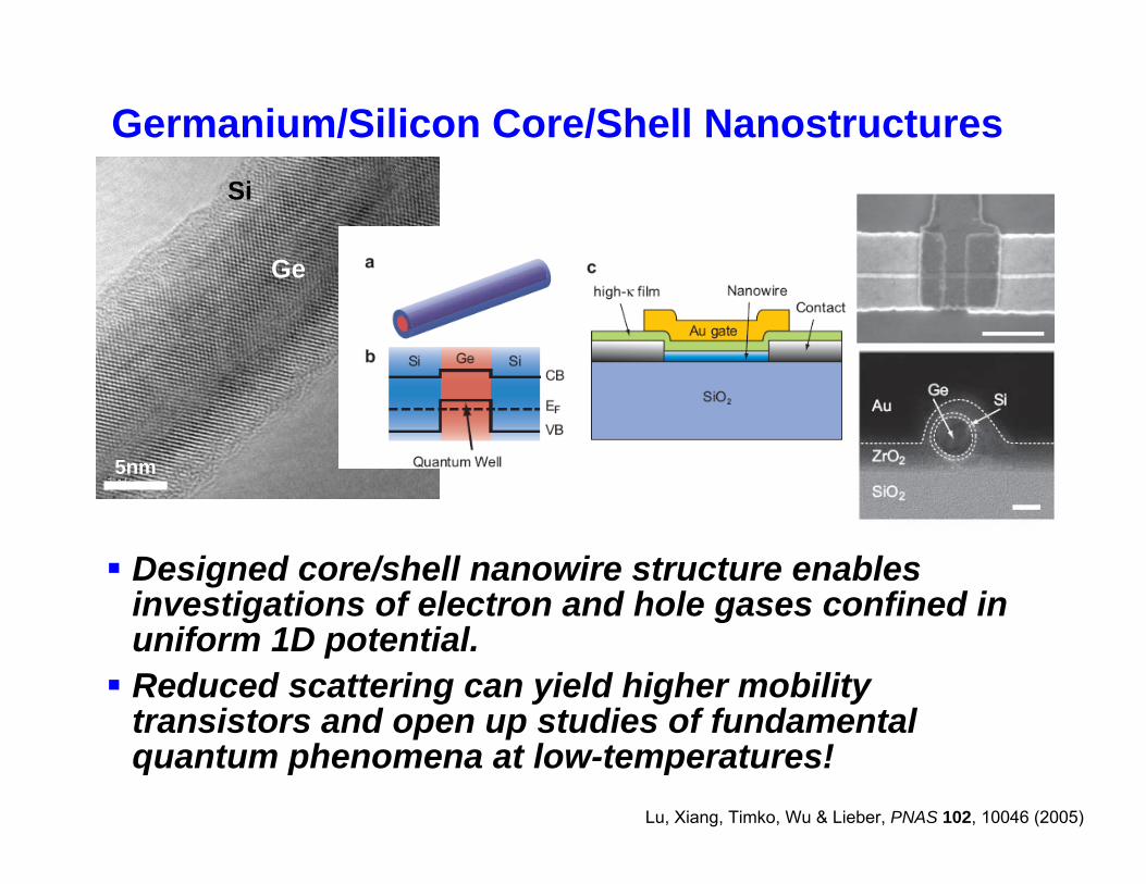
Germanium/Silicon Core/Shell Nanostructures
Lu, Xiang, Timko, Wu & Lieber, PNAS 102, 10046 (2005)
Designed core/shell nanowire structure enables investigations of electron and hole gases confined in uniform 1D potential.Reduced scattering can yield higher mobility transistors and open up studies of fundamental quantum phenomena at low-temperatures!
5nm
Si
Ge
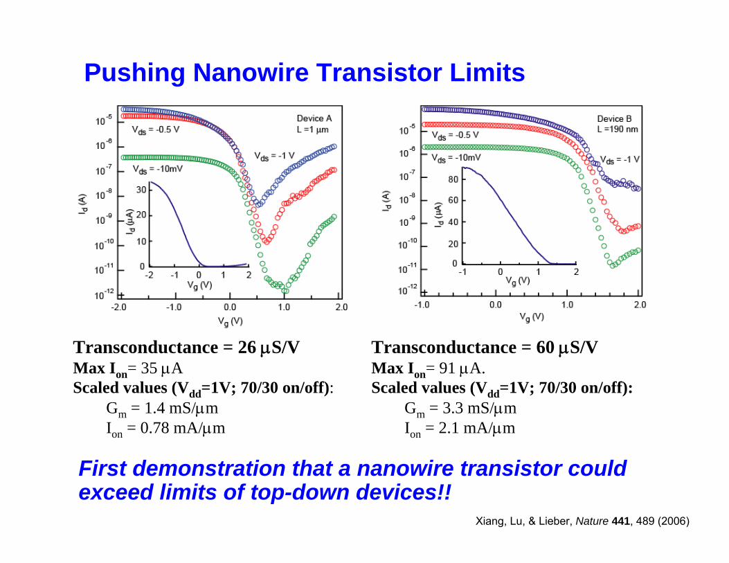
Pushing Nanowire Transistor Limits
Transconductance = 26 μS/VMax Ion= 35 μAScaled values (Vdd=1V; 70/30 on/off):
Gm = 1.4 mS/μmIon = 0.78 mA/μm
Transconductance = 60 μS/VMax Ion= 91 μA. Scaled values (Vdd=1V; 70/30 on/off):
Gm = 3.3 mS/μmIon = 2.1 mA/μm
Xiang, Lu, & Lieber, Nature 441, 489 (2006)
First demonstration that a nanowire transistor could exceed limits of top-down devices!!
Nanowire FETs: How Good Are They?
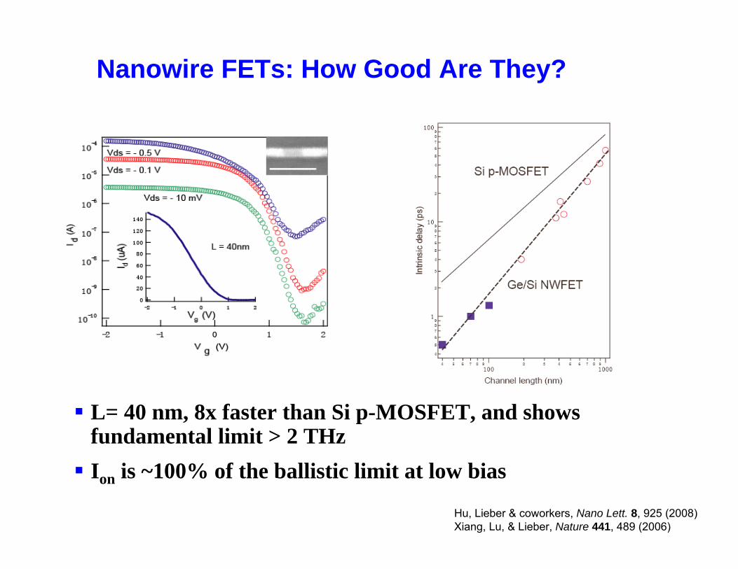
Transconductance = 182 μS/VMax Ion= 152 μAScaled values (Vdd=0.5V; 70/30 on/off):
Gm = 5.0 mS/μmIon = 1.7 mA/μm
S = 160 mV/decade
L= 40 nm, 8x faster than Si p-MOSFET, and shows fundamental limit > 2 THzIon is ~100% of the ballistic limit at low bias
Hu, Lieber & coworkers, Nano Lett. 8, 925 (2008)Xiang, Lu, & Lieber, Nature 441, 489 (2006)
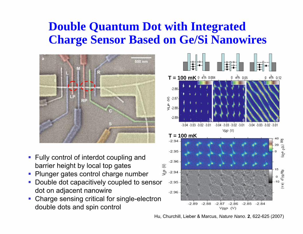
Fully control of interdot coupling and barrier height by local top gatesPlunger gates control charge numberDouble dot capacitively coupled to sensor dot on adjacent nanowireCharge sensing critical for single-electron double dots and spin control
Double Quantum Dot with Integrated Charge Sensor Based on Ge/Si Nanowires
Hu, Churchill, Lieber & Marcus, Nature Nano. 2, 622-625 (2007)
T = 100 mK
T = 100 mK
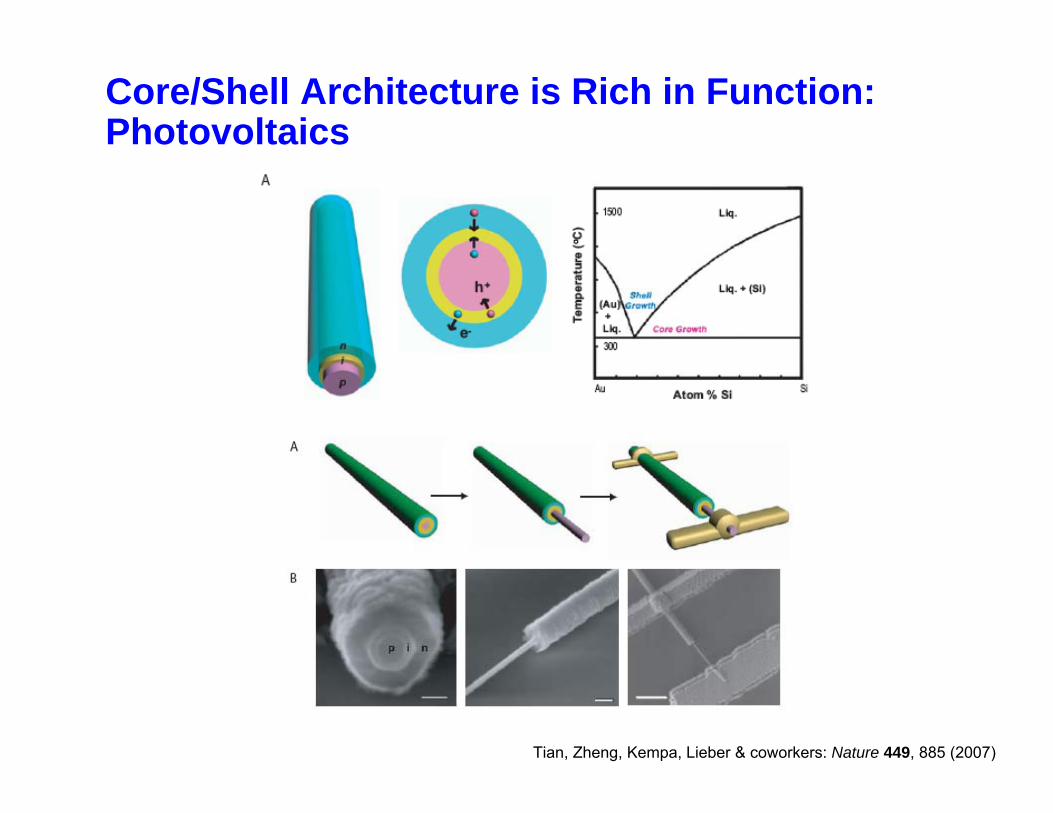
Core/Shell Architecture is Rich in Function: Photovoltaics
p-type/intrinsic/n-type (p-i-n) core/shell/shell silicon nanowires in which the structure and composition of the core and shells are readily controlled. Radial structures might enable improved carrier collection and overall efficiency, comparable to single crystal semiconductors,while retaining solution processing of nanoparticle and organic systems.
Tian, Zheng, Kempa, Lieber & coworkers: Nature 449, 885 (2007)
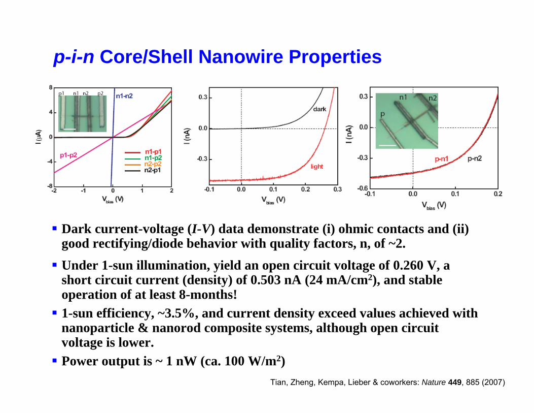
p-i-n Core/Shell Nanowire Properties
Dark current-voltage (I-V) data demonstrate (i) ohmic contacts and (ii) good rectifying/diode behavior with quality factors, n, of ~2.Under 1-sun illumination, yield an open circuit voltage of 0.260 V, a short circuit current (density) of 0.503 nA (24 mA/cm2), and stable operation of at least 8-months!1-sun efficiency, ~3.5%, and current density exceed values achieved with nanoparticle & nanorod composite systems, although open circuit voltage is lower.Power output is ~ 1 nW (ca. 100 W/m2)
Tian, Zheng, Kempa, Lieber & coworkers: Nature 449, 885 (2007)
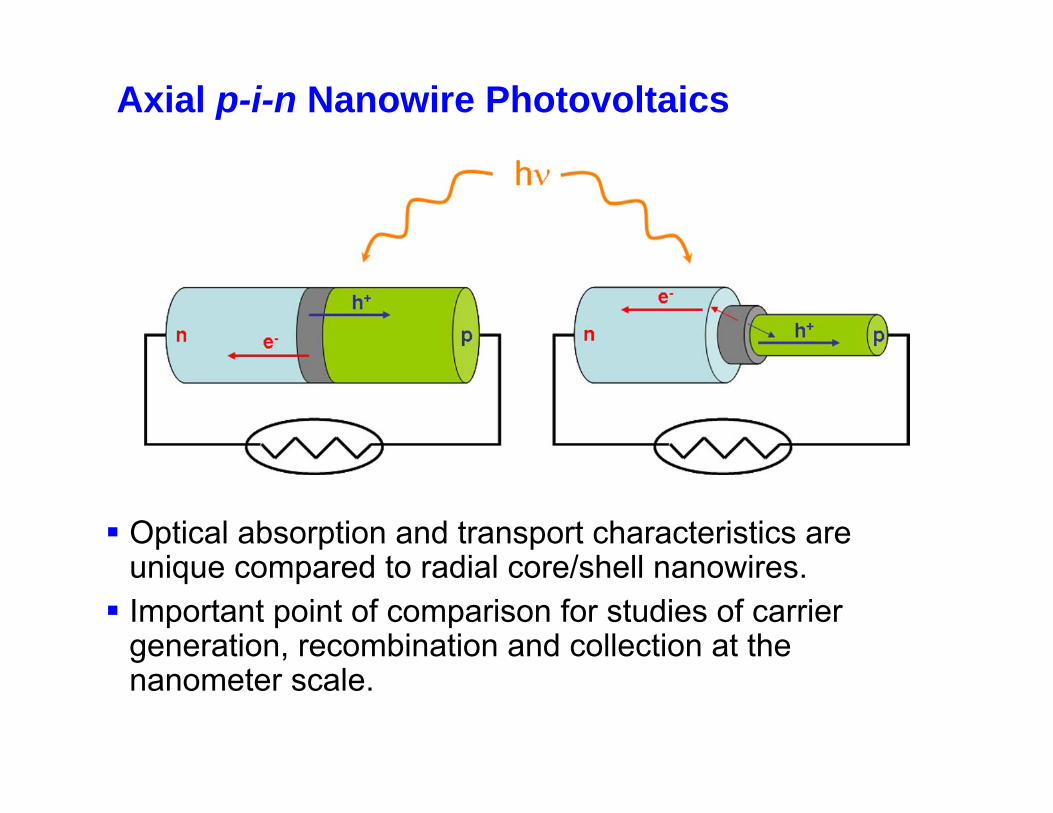
Axial p-i-n Nanowire Photovoltaics
Optical absorption and transport characteristics are unique compared to radial core/shell nanowires. Important point of comparison for studies of carrier generation, recombination and collection at the nanometer scale.
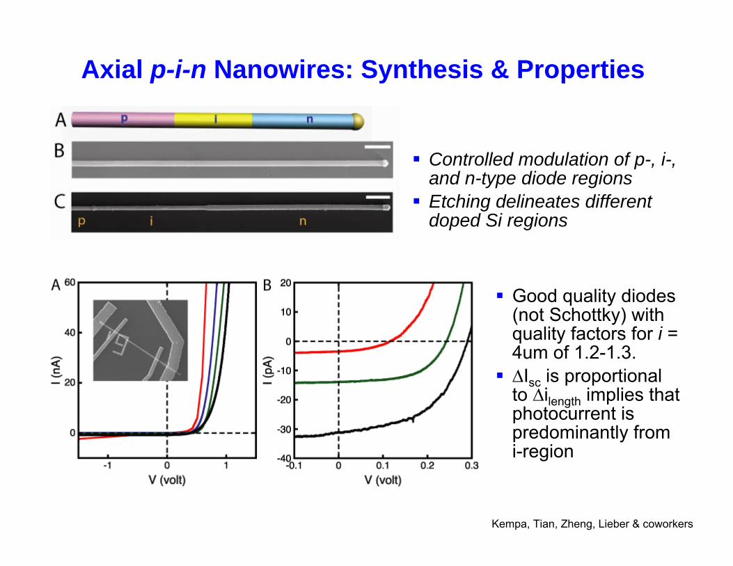
Axial p-i-n Nanowires: Synthesis & Properties
Controlled modulation of p-, i-, and n-type diode regionsEtching delineates different doped Si regions
Kempa, Tian, Zheng, Lieber & coworkers
Good quality diodes (not Schottky) with quality factors for i = 4um of 1.2-1.3.∆Isc is proportional to ∆ilength implies that photocurrent is predominantly from i-region
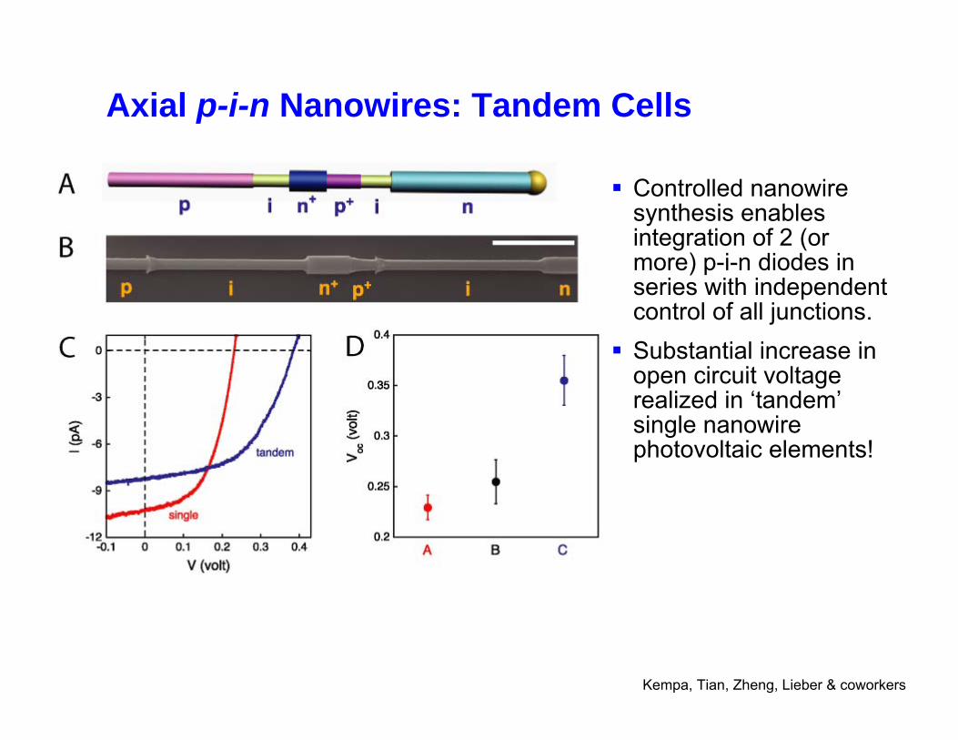
Axial p-i-n Nanowires: Tandem Cells
Controlled nanowire synthesis enables integration of 2 (or more) p-i-n diodes in series with independent control of all junctions.Substantial increase in open circuit voltage realized in ‘tandem’single nanowire photovoltaic elements!
Kempa, Tian, Zheng, Lieber & coworkers
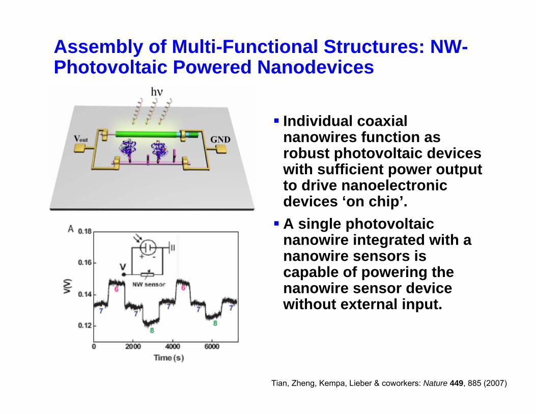
Individual coaxial nanowires function as robust photovoltaic devices with sufficient power output to drive nanoelectronic devices ‘on chip’.A single photovoltaic nanowire integrated with a nanowire sensors is capable of powering the nanowire sensor device without external input.
Tian, Zheng, Kempa, Lieber & coworkers: Nature 449, 885 (2007)
Assembly of Multi-Functional Structures: NW-Photovoltaic Powered Nanodevices
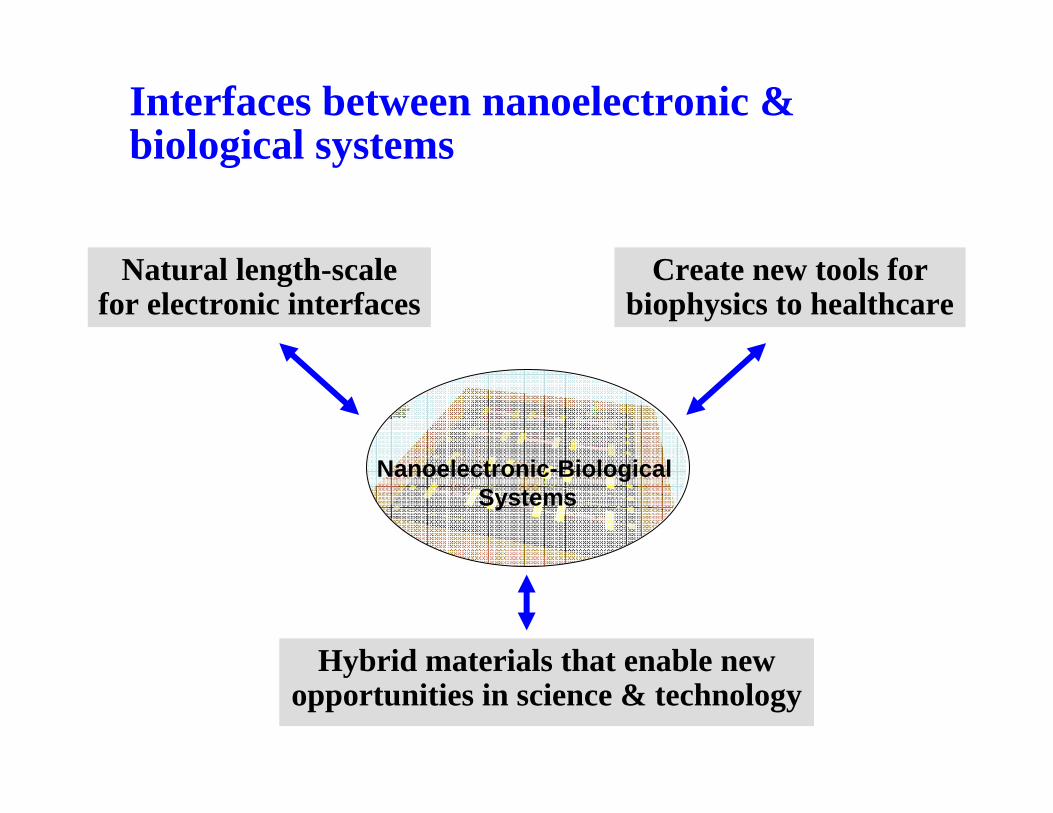
Interfaces between nanoelectronic & biological systems
Natural length-scale for electronic interfaces
Nanoelectronic-Biological Systems
Create new tools for biophysics to healthcare
Hybrid materials that enable new opportunities in science & technology
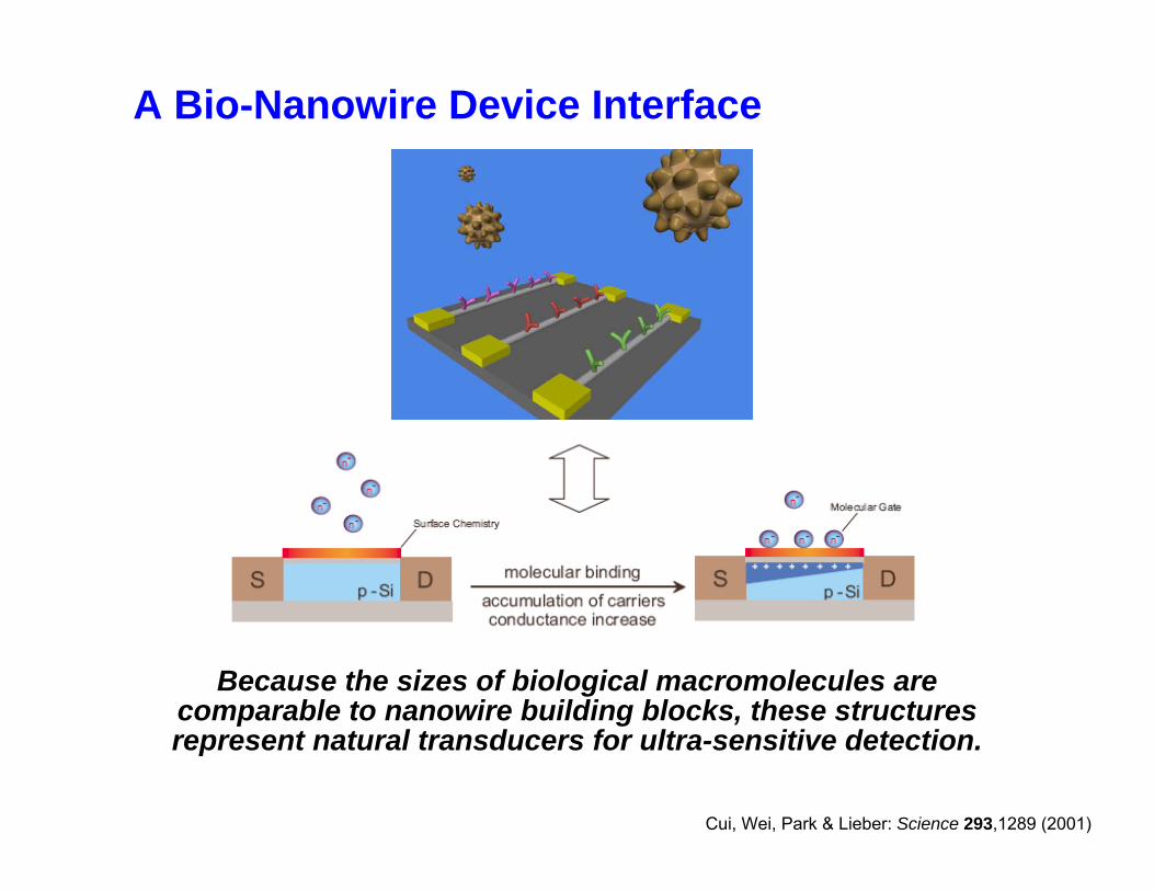
A Bio-Nanowire Device Interface
Planar FET
Cui, Wei, Park & Lieber: Science 293,1289 (2001)
Because the sizes of biological macromolecules are comparable to nanowire building blocks, these structures represent natural transducers for ultra-sensitive detection.
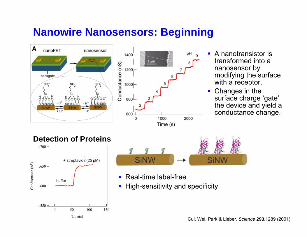
Nanowire Nanosensors: Beginning
A nanotransistor is transformed into a nanosensor by modifying the surface with a receptor.Changes in the surface charge ‘gate’the device and yield a conductance change.
Cui, Wei, Park & Lieber, Science 293,1289 (2001)
+ streptavidin(25 pM)
buffer
Detection of Proteins
Real-time label-free High-sensitivity and specificity
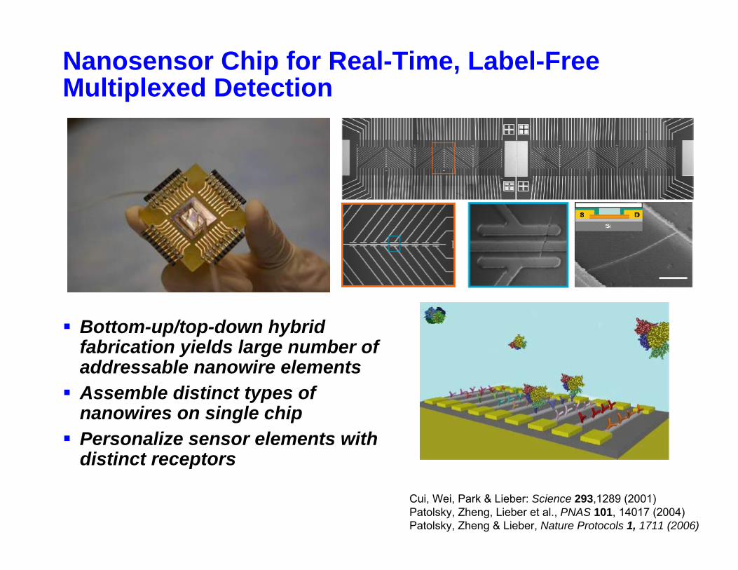
Nanosensor Chip for Real-Time, Label-Free Multiplexed Detection
Bottom-up/top-down hybrid fabrication yields large number of addressable nanowire elementsAssemble distinct types of nanowires on single chipPersonalize sensor elements with distinct receptors
Cui, Wei, Park & Lieber: Science 293,1289 (2001)Patolsky, Zheng, Lieber et al., PNAS 101, 14017 (2004)Patolsky, Zheng & Lieber, Nature Protocols 1, 1711 (2006)
Buffer
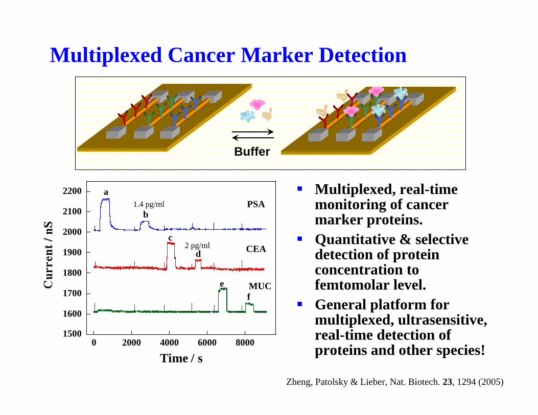
Multiplexed Cancer Marker Detection
1500
1600
1700
1800
1900
2000
2100
2200
0 2000 4000 6000 8000
Time / s
a
b
c
d
ef
PSA
CEA
MUC
Multiplexed, real-time monitoring of cancer marker proteins.Quantitative & selective detection of protein concentration to femtomolar level.General platform for multiplexed, ultrasensitive, real-time detection of proteins and other species!
1.4 pg/ml
2 pg/ml
Zheng, Patolsky & Lieber, Nat. Biotech. 23, 1294 (2005)
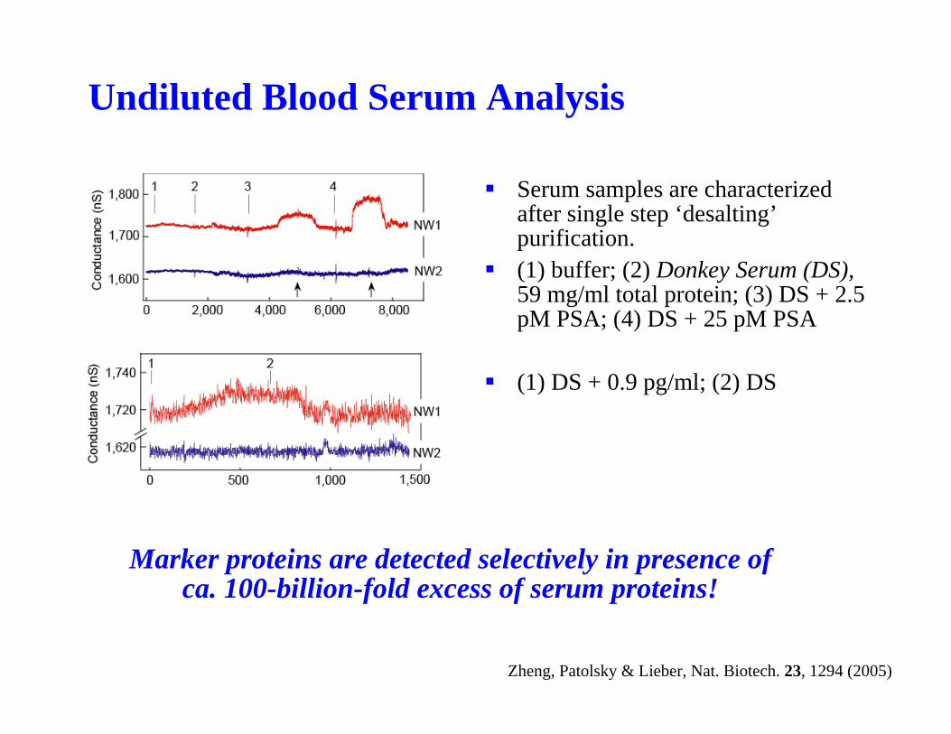
Undiluted Blood Serum Analysis
Serum samples are characterized after single step ‘desalting’purification. (1) buffer; (2) Donkey Serum (DS),59 mg/ml total protein; (3) DS + 2.5 pM PSA; (4) DS + 25 pM PSA
(1) DS + 0.9 pg/ml; (2) DS
Zheng, Patolsky & Lieber, Nat. Biotech. 23, 1294 (2005)
Marker proteins are detected selectively in presence of ca. 100-billion-fold excess of serum proteins!
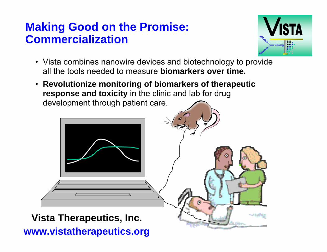
• Vista combines nanowire devices and biotechnology to provide all the tools needed to measure biomarkers over time.
• Revolutionize monitoring of biomarkers of therapeutic response and toxicity in the clinic and lab for drug development through patient care.
Making Good on the Promise: Commercialization
Vista Therapeutics, Inc.www.vistatherapeutics.org
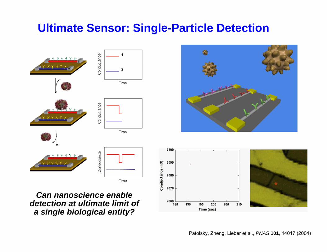
Ultimate Sensor: Single-Particle Detection
Can nanoscience enable detection at ultimate limit of a single biological entity?
Patolsky, Zheng, Lieber et al., PNAS 101, 14017 (2004)
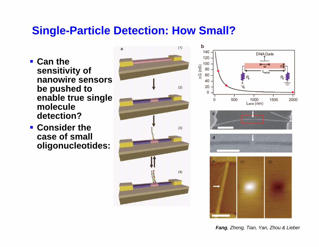
Single-Particle Detection: How Small?
Can the sensitivity of nanowire sensors be pushed to enable true single molecule detection?Consider the case of small oligonucleotides:
Fang, Zheng, Tian, Yan, Zhou & Lieber
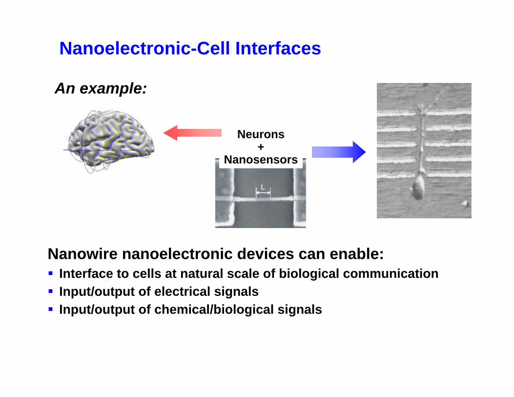
Nanoelectronic-Cell Interfaces
Neurons+
Nanosensors
Nanowire nanoelectronic devices can enable:Interface to cells at natural scale of biological communicationInput/output of electrical signalsInput/output of chemical/biological signals
An example:
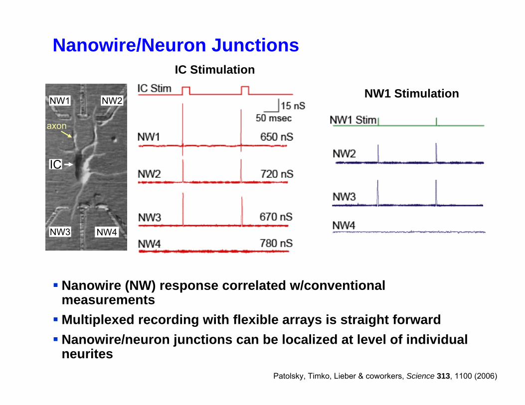
Nanowire/Neuron Junctions
NW1 NW2
NW3 NW4
axon
IC
IC Stimulation
NW1 Stimulation
Nanowire (NW) response correlated w/conventional measurementsMultiplexed recording with flexible arrays is straight forwardNanowire/neuron junctions can be localized at level of individual neurites
Patolsky, Timko, Lieber & coworkers, Science 313, 1100 (2006)
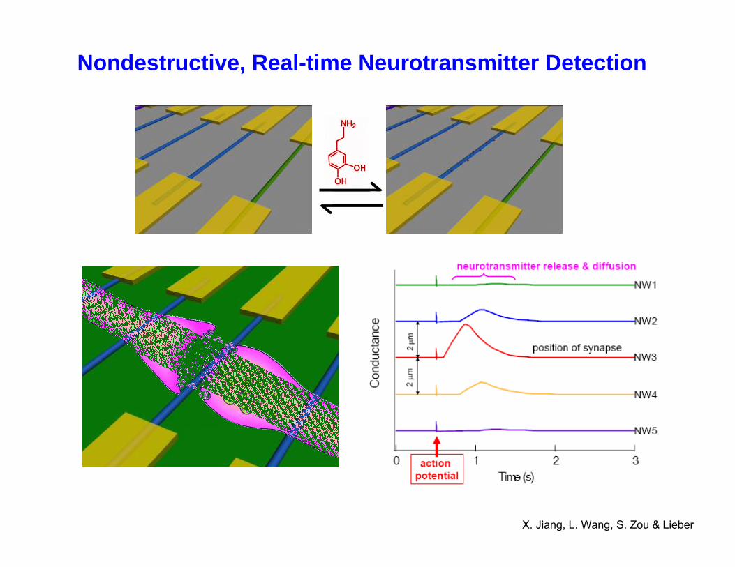
Nondestructive, Real-time Neurotransmitter Detection
X. Jiang, L. Wang, S. Zou & Lieber
Selective detection of neurotransmitter dopamine to at least 100 fM sensitivity Reversible & nondestructivePotential for high spatial and temporal resolutionPotential for simultaneous neurotransmitter & action potential recording
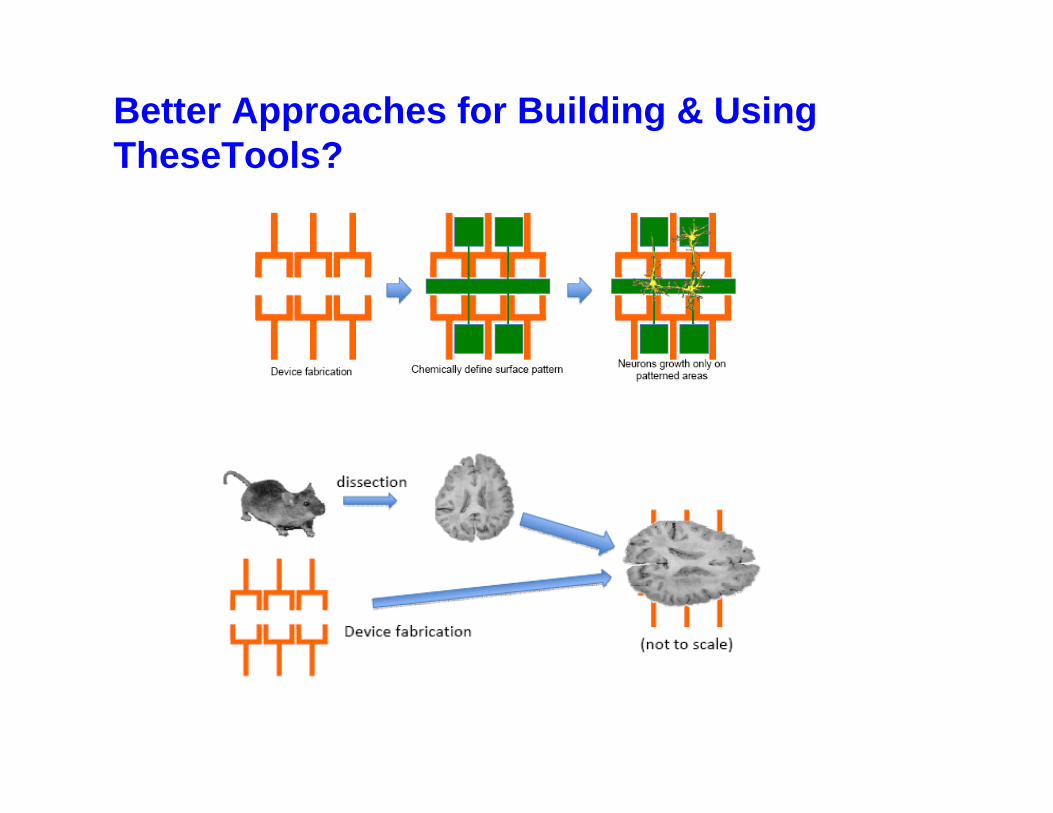
Better Approaches for Building & Using TheseTools?
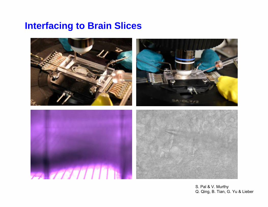
Interfacing to Brain Slices
S. Pal & V. MurthyQ. Qing, B. Tian, G. Yu & Lieber
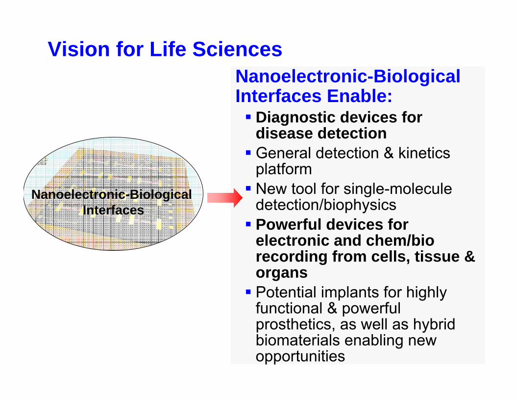
Vision for Life SciencesNanoelectronic-Biological Interfaces Enable:
Diagnostic devices for disease detectionGeneral detection & kinetics platform New tool for single-molecule detection/biophysicsPowerful devices for electronic and chem/bio recording from cells, tissue & organsPotential implants for highly functional & powerful prosthetics, as well as hybrid biomaterials enabling new opportunities
Nanoelectronic-Biological Interfaces
Evaluating Research Motivation: Progress?
Synthetic challenge of controlling structure and composition on many length scalesFundamental scientific questions in 1-dimensional systemsCentral importance of nanoscale wires in integrated nanosystemsNew/novel materials can make revolutionary vs. evolutionary changes in science and technology!
⇒ Many fundamental scientific questions remain, and will require bold researchers to address.
⇒ Pushing ourselves to identify and tackle these ‘big’challenges, while difficult, offers the best opportunity to make revolutionary advances and benefit society!
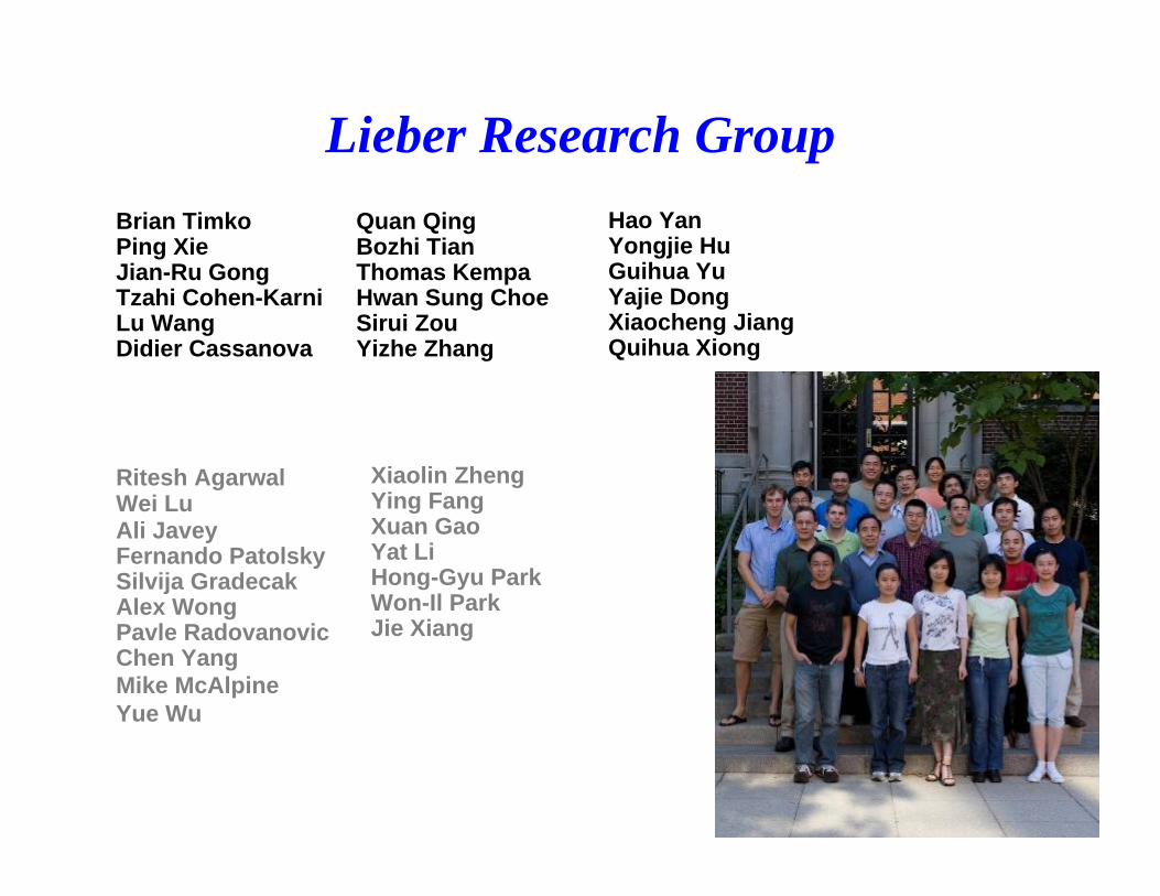
Lieber Research GroupBrian TimkoPing XieJian-Ru GongTzahi Cohen-KarniLu WangDidier Cassanova
Quan QingBozhi TianThomas KempaHwan Sung ChoeSirui ZouYizhe Zhang
Hao YanYongjie HuGuihua YuYajie DongXiaocheng JiangQuihua Xiong
Xiaolin ZhengYing Fang Xuan GaoYat LiHong-Gyu Park Won-Il ParkJie Xiang
Ritesh AgarwalWei LuAli JaveyFernando PatolskySilvija GradecakAlex Wong Pavle RadovanovicChen Yang Mike McAlpineYue Wu