Embed Size (px)
Citation preview
Nanoscale
PAPER
Cite this: DOI: 10.1039/c4nr01914h
Received 9th April 2014,Accepted 12th October 2014
DOI: 10.1039/c4nr01914h
www.rsc.org/nanoscale
Nanowire-based multifunctional antireflectioncoatings for solar cells†
Pritesh Hiralal,*a Chihtao Chien,a Niraj N. Lal,b Waranatha Abeygunasekara,a,c
Abhishek Kumar,a Haider Butt,d Hang Zhou,e Husnu Emrah Unalan,f
Jeremy J. Baumbergb and Gehan A. J. Amaratungaa
Organic (P3HT/PCBM) solar cells are coated with ZnO nanowires as antireflection coatings and show up
to 36% enhancement in efficiency. The improvement is ascribed to an effective refractive index which
results in Fabry–Perot absorption bands which match the polymer band-gap. The effect is particularly
pronounced at high light incidence angles. Simultaneously, the coating is used as a UV-barrier, demon-
strating a 50% reduction in the rate of degradation of the polymers under accelerated lifetime testing. The
coating also allows the surface of the solar cell to self-clean via two distinct routes. On one hand, photo-
catalytic degradation of organic material on ZnO is enhanced by the high surface area of the nanowires
and quantified by dye degradation measurements. On the other, the surface of the nanowires can be
functionalized to tune the water contact angle from superhydrophilic (16°) to superhydrophobic (152°),
resulting in self-cleaning via the Lotus effect. The multifunctional ZnO nanowires are grown by a low cost,
low temperature hydrothermal method, compatible with process limitations of organic solar cells.
Introduction
The last few years have seen a fourfold drop in the moduleprice of solar cells.1 Accompanied by high energy costs, photo-voltaic (PV) energy has become an economically attractive can-didate in many high insolation/high energy cost locationsaround the planet. Further reductions in cost and improve-ments in conversion efficiency are fundamental to furtherextend the range of locations in which photovoltaic energy isan economically sound option.
The current output of a photovoltaic cell depends princi-pally on two factors; on the likelihood of an incident photonbeing absorbed, generating electron–hole pairs, and on theprobability of the charge carriers being collected. The necessity
of lowering costs is driving reduction in PV cell thickness,reducing the use of material as well as permitting the use ofcheaper, low diffusion-length materials as the absorbing base.
Organic solar cells are a good example with rapidly improv-ing efficiencies.2 In a typical organic solar cell, light absorptioncreates strongly bound excitons that must be dissociated intofree charges at a donor/acceptor interface. This need forexciton dissociation (diffusion length ∼10 nm) complicates thedesign and fabrication of efficient organic solar cells, limitingthe thickness of organic films to around 100 nm, whichdespite strong absorption, is insufficient to utilize most of theincoming light, particularly at longer wavelengths. The keysolution is to enhance the optical path length by strongly trap-ping light within the cell. Various light trapping techniqueshave been proposed and explored. Electromagnetic fieldoptimization by adjusting film thicknesses allows absorptionto be increased.3 Periodic gratings4 can form oblique anglediffractions but are ineffective in preventing big reflectionlosses, and Bragg reflectors,5 while having high reflectivity, canonly double the optical path length. Photonic crystal backreflectors have been shown to increase optical path length bytwo orders of magnitude.6 Surface plasmons in nanoscalemetals have also been exploited to enhance absorption in PVcells.7–9 Additionally, randomly or periodically nanostructuredmaterials10,11 have emerged as specific building blocks forconstructing light-trapping assemblies.
Nanowire arrays show anti-reflective and light trapping pro-perties; silicon NW arrays of a few microns in length have been
†Electronic supplementary information (ESI) available. See DOI: 10.1039/c4nr01914h
aCentre of Advanced Photonics and Electronics, Department of Engineering,
University of Cambridge, 9 JJ Thomson Av., CB3 0FA Cambridge, UK.
E-mail: [email protected]; Fax: +44 (0)1223 748348; Tel: +44 (0)1223 748325bNanoPhotonics Centre, Cavendish Laboratory, University of Cambridge, CB3 0HE
Cambridge, UKcDepartment of Electrical and Electronic Engineering, University of Peradeniya,
Sri LankadSchool of Mechanical Engineering, University of Birmingham, Birmingham B15 2TT,
UKeSchool of Electronic and Computer Engineering, Peking University, Shenzhen
Graduate School, ChinafDepartment of Metallurgical and Materials Engineering, Middle East Technical
University, Ankara, Turkey
This journal is © The Royal Society of Chemistry 2014 Nanoscale
Publ
ishe
d on
13
Oct
ober
201
4. D
ownl
oade
d by
Aus
tral
ian
Nat
iona
l Uni
vers
ity o
n 06
/11/
2014
05:
55:1
7.
View Article OnlineView Journal
noted for their strong broadband optical absorption acrossmultiple incident angles and their dark visual appearance.12–14
This reduction in reflectance seems to be a common character-istic of nanowire arrays.15–17
Textured ZnO films by metalorganic chemical vapor depo-sition where considered as anti-reflection (AR) coatings earlyon.18 ZnO has a wurtzite structure and due to the surface ener-getics of its crystal facets, easily grows as NWs.19 The dimen-sions of these NWs can be easily controlled by the processparameters, and they can be produced at low temperaturesand large scales,20 making them attractive candidates forphotovoltaic antireflection coatings.21 ZnO NWs have alreadybeen coated onto Si solar cells,22,23 demonstrating someimprovement in efficiency.
In this work, we demonstrate ZnO NWs as antireflectioncoatings on organic photovoltaic cells for the first time. The ZnONW coating brings additional benefits to photovoltaic cells, notpreviously studied in conjunction, namely UV protection andself-cleaning. The band-gap of ZnO (3.2 eV, ∼380 nm) is justsufficient to absorb in the ultraviolet (UV) region. The organiccomponents in OPVs are known to degrade in short times (fewhours) under the combined presence of UV and O2 or H2O.
24
We demonstrate the ZnO coating lowers the UV componentreaching the organic layer and reduces the rate of degradationof the cell. ZnO is a photocatalytic semiconductor; the UV itabsorbs in turn generates charge carriers which can be used tocatalyse redox reactions in the presence of O2 and water, per-mitting the breakdown of organic molecules on its surface.25
This can be used as a self-cleaning mechanism for organicstains, addressing long term yield reduction issues fromsoiling.26
As grown ZnO is naturally superhydrophilic, however, ade-quate surface functionalisation can be used to lower surfaceenergy, which combined with the high surface area of the NWcoating yields a superhydrophobic structure.27 in which thewater–ZnO interface becomes energetically unfavourable andrain water droplets would simply roll off the surface, carryingdirt particles with them, known as the ‘Lotus effect’.28
All three effects, namely AR, UV barrier and self-cleaningare demonstrated and characterized using the same ZnO NW
coating over an organic solar cell. The AR properties are morepronounced when the incoming light is offset from normalincidence, which under a practical scenario forms the majorpart of a solar cells active life. The growth method used (hydro-thermal) uses mild conditions and is compatible with thethermal tolerances of organic PV.
Experimental methodZnO nanowire growth
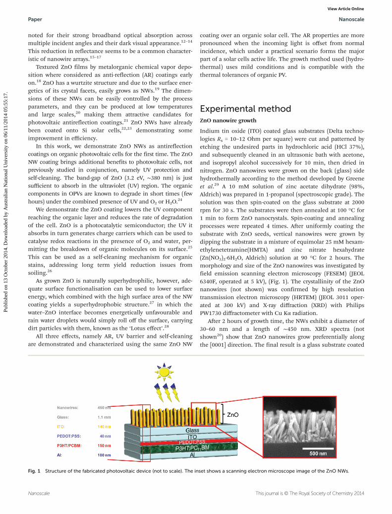
Indium tin oxide (ITO) coated glass substrates (Delta techno-logies Rs = 10–12 Ohm per square) were cut and patterned byetching the undesired parts in hydrochloric acid (HCl 37%),and subsequently cleaned in an ultrasonic bath with acetone,and isopropyl alcohol successively for 10 min, then dried innitrogen. ZnO nanowires were grown on the back (glass) sidehydrothermally according to the method developed by Greeneet al.29 A 10 mM solution of zinc acetate dihydrate (98%,Aldrich) was prepared in 1-propanol (spectroscopic grade). Thesolution was then spin-coated on the glass substrate at 2000rpm for 30 s. The substrates were then annealed at 100 °C for1 min to form ZnO nanocrystals. Spin-coating and annealingprocesses were repeated 4 times. After uniformly coating thesubstrate with ZnO seeds, vertical nanowires were grown bydipping the substrate in a mixture of equimolar 25 mM hexam-ethylenetetramine(HMTA) and zinc nitrate hexahydrate(Zn(NO3)2·6H2O, Aldrich) solution at 90 °C for 2 hours. Themorphology and size of the ZnO nanowires was investigated byfield emission scanning electron microscopy (FESEM) (JEOL6340F, operated at 5 kV), (Fig. 1). The crystallinity of the ZnOnanowires (not shown) was confirmed by high resolutiontransmission electron microscopy (HRTEM) (JEOL 3011 oper-ated at 300 kV) and X-ray diffraction (XRD) with PhilipsPW1730 diffractometer with Cu Kα radiation.
After 2 hours of growth time, the NWs exhibit a diameter of30–60 nm and a length of ∼450 nm. XRD spectra (notshown20) show that ZnO nanowires grow preferentially alongthe [0001] direction. The final result is a glass substrate coated
Fig. 1 Structure of the fabricated photovoltaic device (not to scale). The inset shows a scanning electron microscope image of the ZnO NWs.
Paper Nanoscale
Nanoscale This journal is © The Royal Society of Chemistry 2014
Publ
ishe
d on
13
Oct
ober
201
4. D
ownl
oade
d by
Aus
tral
ian
Nat
iona
l Uni
vers
ity o
n 06
/11/
2014
05:
55:1
7.
View Article Online
with patterned ITO on one side and vertically aligned ZnONWs on the other.
Organic photovoltaic device fabrication
The active material of the organic photovoltaic devices was pre-pared by dissolving [6,6]-phenyl-C61-butyric acid methyl ester(PCBM, Solenne) in dichlorobenzene and then blending regiore-gular poly(3-hexylthiophene-2,5-diyl) (P3HT, Sepiloid P200, RiekeMetals) with an average molecular weight, Mw = 20–30 K, withoutfurther purification. The resulting solution of 64 mg ml−1 con-centration at 1 : 1 ratio was left stirring overnight at 45 °C.
Poly(3,4-ethylenedioxythiophene) poly(styrenesulfonate),(PEDOT–PSS, Baytron P 4083) was deposited by spin coating at5000 rpm onto the pre-patterned ITO substrate and then driedat 135 °C for 15 min, resulting in a 40 nm film. Subsequently,the devices where moved into a N2 glovebox for deposition ofthe photoactive layer. The P3HT–PCBM solution was depositedby spin casting at 1300 rpm. 100 nm thick Al electrodes weredeposited via thermal evaporation (pressure ∼3 × 10⁻⁶ Torr),resulting in active device areas of 8 mm2. After evaporation,the devices were further annealed at 150 °C for 5 minutes. Thestructure of the resulting device is shown in Fig. 1. Typically,8 devices were fabricated per substrate and each individualsubstrate had 4 of the 8 devices covered with ZnO NWs, inorder to minimise interdevice variations.
The solar cells were characterized immediately after fabrica-tion in ambient air environment at room temperature. Externalquantum efficiency (EQE) spectra were measured using a 100 Wtungsten halogen lamp, dispersed through a monochromator.A Keithley 237 source measure unit was used to measure theshort circuit current as a function of wavelength. The incidentlight intensity was continuously monitored during measure-ment by a reference photodiode calibrated by placing a Hama-matsu S8746-01 calibrated photodiode at the sample position.The current–voltage (I–V) characteristics of the devices weremeasured using a computer controlled HP 4140 source meter.An AM 1.5 solar simulator (Oriel 67005 with AM1.5 filter) at100 mW cm−1 was used as the illumination source.
Results and discussionAntireflection
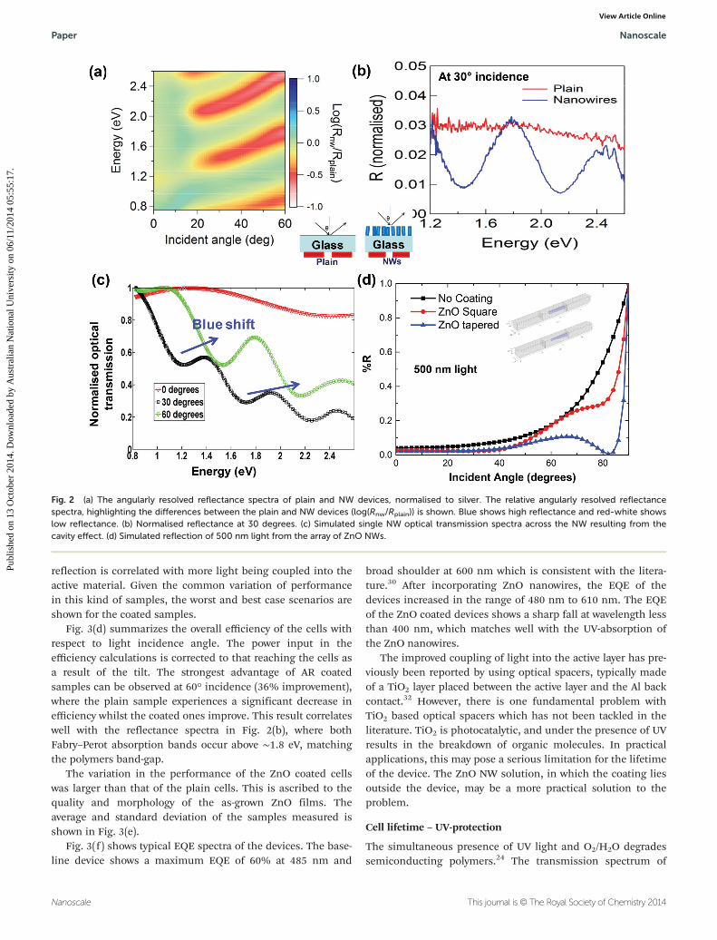
Angularly resolved reflectivity measurements (Fig. 2(a) and (b))were taken with a supercontinuum white-light laser obtainedvia the non-linear dispersion of a passively mode locked1064 microchip laser (JDS Uniphase) focused through a holeyfibre (Blaze Photonics). The beam has mixed polarization witha wavelength range of 500–1500 nm and angle range of 0–60degrees. Results displayed are the log of reflectance, normal-ised to flat silver. The power of the beam is <1 mW and the col-lection area is approximately 200 µm in diameter.
NWs act as an anti-reflection coating by providing aneffective refractive index between air and ITO glass. Angularlyresolved reflectance of the NW coated sample shows distinctFabry–Perot absorption bands (red-white curves), which
undergo a typical blue shift (increase in frequency) withincrease in incidence angle. The absorption enhancementoccurs at energies which are typical of the band-gap of poly-mers used for OPVs (∼1.9 eV).
Finite element method (FEM) simulations were carried outto simulate the wave propagation across a single ZnO nanowireand to understand absorption bands. To demonstrate that theZnO NWs act as cavity towards the incident light (producingthe blue shifting absorption bands) and for the purpose ofsimplification a single NW with a radius of 40 nm and height0.45 μm (average value) was simulated in a three dimensionalgeometry. Non-periodic/scattering boundary conditions wereused around the NW. The NW was illuminated with a planewave light source in the range of around 478 nm to 1500 nm(∼0.83 eV to 2.6 eV). The light was polarized parallel (TMmode) to the NW. Simulations were performed for incidenceangles of 0, 30 and 60 degrees with the vertical. Fig. 2(c) showsthe transmission spectra simulated for the three incidentangles. The spectrum for zero degrees shows only two weakresonant cavity modes for the NW. However, at 30 and 60degrees a number of cavity modes were coupled into the NWs.For the incident angle of 30 degrees resonant modes wereobserved at around 1.40,1.90 and 2.45 eV. For the 60 degreesincident light resonant modes were observed at around 1.8and 2.5 eV. The resonant peaks were observed to blue shiftwith the increase in incident angle. These results demonstratethe cavity resonance of the ZnO nanowire and explain theabsorption bands in the measured spectra. However, in theexperiments an average cavity effect of many NWs resonatingsimultaneously is observed. As not all the NWs are orientednormally, due to which they resonate at a slightly differentwavelengths for a certain incidence angle of light. Both theeffects result in the broadening of the experimentallymeasured absorption bands.
Distribution in NW length results in an overall gradeddensity and effective refractive from the glass towards the airinterface. Fig. 2d shows the results from a simulation in whicha periodic condition is applied. ZnO nanowires were rep-resented as a periodic array nanowires of square shaped crosssection. The simulation was done for nanowires of uniformcross section and also for tapering cross sections to take theoverall graded nature into account. A good correlation isobserved with experimental data (Fig. 2a).
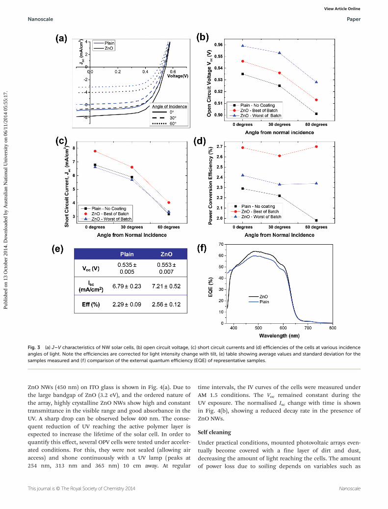
J–V characteristics of OPV cells with and without ZnOcoating are shown in Fig. 3(a) for different angles of incidenceof the light. The light source intensity and position is main-tained constant throughout the experiments, and the inci-dence angle was changed by tilting the solar cells. In effect,this resulted in a lower intensity of light reaching the cellsupon tilting. A ∼17% enhancement in efficiency is observed atnormal incidence for the NW samples. The ZnO coatedsamples consistently had a larger open circuit voltage, andtypically a larger short circuit current than the plain, referencesamples (Fig. 3(b) and (c)). The light intensity dependence ofVoc has been previously explained,31 and together with theincrease in Jsc with the coating, suggests that the reduced
Nanoscale Paper
This journal is © The Royal Society of Chemistry 2014 Nanoscale
Publ
ishe
d on
13
Oct
ober
201
4. D
ownl
oade
d by
Aus
tral
ian
Nat
iona
l Uni
vers
ity o
n 06
/11/
2014
05:
55:1
7.
View Article Online
reflection is correlated with more light being coupled into theactive material. Given the common variation of performancein this kind of samples, the worst and best case scenarios areshown for the coated samples.
Fig. 3(d) summarizes the overall efficiency of the cells withrespect to light incidence angle. The power input in theefficiency calculations is corrected to that reaching the cells asa result of the tilt. The strongest advantage of AR coatedsamples can be observed at 60° incidence (36% improvement),where the plain sample experiences a significant decrease inefficiency whilst the coated ones improve. This result correlateswell with the reflectance spectra in Fig. 2(b), where bothFabry–Perot absorption bands occur above ∼1.8 eV, matchingthe polymers band-gap.
The variation in the performance of the ZnO coated cellswas larger than that of the plain cells. This is ascribed to thequality and morphology of the as-grown ZnO films. Theaverage and standard deviation of the samples measured isshown in Fig. 3(e).
Fig. 3(f ) shows typical EQE spectra of the devices. The base-line device shows a maximum EQE of 60% at 485 nm and
broad shoulder at 600 nm which is consistent with the litera-ture.30 After incorporating ZnO nanowires, the EQE of thedevices increased in the range of 480 nm to 610 nm. The EQEof the ZnO coated devices shows a sharp fall at wavelength lessthan 400 nm, which matches well with the UV-absorption ofthe ZnO nanowires.
The improved coupling of light into the active layer has pre-viously been reported by using optical spacers, typically madeof a TiO2 layer placed between the active layer and the Al backcontact.32 However, there is one fundamental problem withTiO2 based optical spacers which has not been tackled in theliterature. TiO2 is photocatalytic, and under the presence of UVresults in the breakdown of organic molecules. In practicalapplications, this may pose a serious limitation for the lifetimeof the device. The ZnO NW solution, in which the coating liesoutside the device, may be a more practical solution to theproblem.
Cell lifetime – UV-protection
The simultaneous presence of UV light and O2/H2O degradessemiconducting polymers.24 The transmission spectrum of
Fig. 2 (a) The angularly resolved reflectance spectra of plain and NW devices, normalised to silver. The relative angularly resolved reflectancespectra, highlighting the differences between the plain and NW devices (log(Rnw/Rplain)) is shown. Blue shows high reflectance and red-white showslow reflectance. (b) Normalised reflectance at 30 degrees. (c) Simulated single NW optical transmission spectra across the NW resulting from thecavity effect. (d) Simulated reflection of 500 nm light from the array of ZnO NWs.
Paper Nanoscale
Nanoscale This journal is © The Royal Society of Chemistry 2014
Publ
ishe
d on
13
Oct
ober
201
4. D
ownl
oade
d by
Aus
tral
ian
Nat
iona
l Uni
vers
ity o
n 06
/11/
2014
05:
55:1
7.
View Article Online
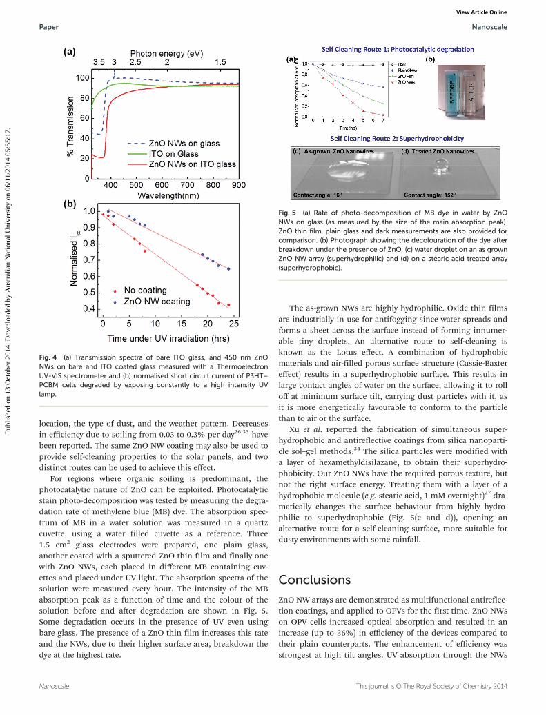
ZnO NWs (450 nm) on ITO glass is shown in Fig. 4(a). Due tothe large bandgap of ZnO (3.2 eV), and the ordered nature ofthe array, highly crystalline ZnO NWs show high and constanttransmittance in the visible range and good absorbance in theUV. A sharp drop can be observed below 400 nm. The conse-quent reduction of UV reaching the active polymer layer isexpected to increase the lifetime of the solar cell. In order toquantify this effect, several OPV cells were tested under acceler-ated conditions. For this, they were not sealed (allowing airaccess) and shone continuously with a UV lamp (peaks at254 nm, 313 nm and 365 nm) 10 cm away. At regular
time intervals, the IV curves of the cells were measured underAM 1.5 conditions. The Voc remained constant during theUV exposure. The normalised Isc change with time is shownin Fig. 4(b), showing a reduced decay rate in the presence ofZnO NWs.
Self cleaning
Under practical conditions, mounted photovoltaic arrays even-tually become covered with a fine layer of dirt and dust,decreasing the amount of light reaching the cells. The amountof power loss due to soiling depends on variables such as
Fig. 3 (a) J–V characteristics of NW solar cells, (b) open circuit voltage, (c) short circuit currents and (d) efficiencies of the cells at various incidenceangles of light. Note the efficiencies are corrected for light intensity change with tilt, (e) table showing average values and standard deviation for thesamples measured and (f ) comparison of the external quantum efficiency (EQE) of representative samples.
Nanoscale Paper
This journal is © The Royal Society of Chemistry 2014 Nanoscale
Publ
ishe
d on
13
Oct
ober
201
4. D
ownl
oade
d by
Aus
tral
ian
Nat
iona
l Uni
vers
ity o
n 06
/11/
2014
05:
55:1
7.
View Article Online
location, the type of dust, and the weather pattern. Decreasesin efficiency due to soiling from 0.03 to 0.3% per day26,33 havebeen reported. The same ZnO NW coating may also be used toprovide self-cleaning properties to the solar panels, and twodistinct routes can be used to achieve this effect.
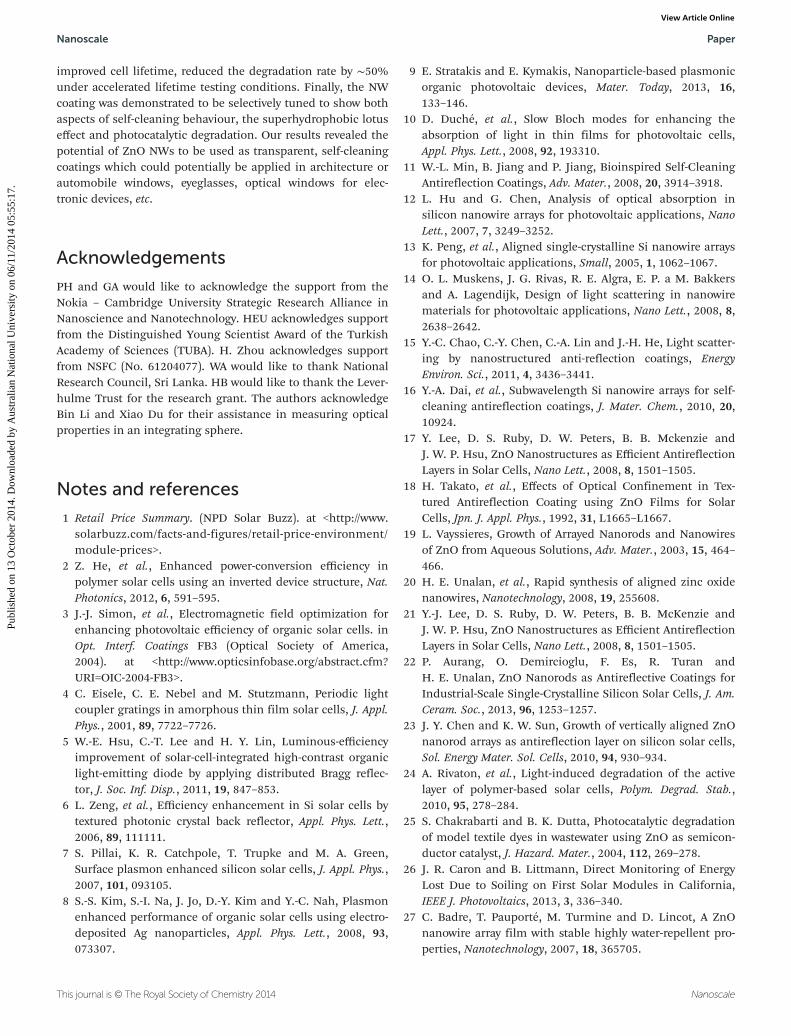
For regions where organic soiling is predominant, thephotocatalytic nature of ZnO can be exploited. Photocatalyticstain photo-decomposition was tested by measuring the degra-dation rate of methylene blue (MB) dye. The absorption spec-trum of MB in a water solution was measured in a quartzcuvette, using a water filled cuvette as a reference. Three1.5 cm2 glass electrodes were prepared, one plain glass,another coated with a sputtered ZnO thin film and finally onewith ZnO NWs, each placed in different MB containing cuv-ettes and placed under UV light. The absorption spectra of thesolution were measured every hour. The intensity of the MBabsorption peak as a function of time and the colour of thesolution before and after degradation are shown in Fig. 5.Some degradation occurs in the presence of UV even usingbare glass. The presence of a ZnO thin film increases this rateand the NWs, due to their higher surface area, breakdown thedye at the highest rate.
The as-grown NWs are highly hydrophilic. Oxide thin filmsare industrially in use for antifogging since water spreads andforms a sheet across the surface instead of forming innumer-able tiny droplets. An alternative route to self-cleaning isknown as the Lotus effect. A combination of hydrophobicmaterials and air-filled porous surface structure (Cassie-Baxtereffect) results in a superhydrophobic surface. This results inlarge contact angles of water on the surface, allowing it to rolloff at minimum surface tilt, carrying dust particles with it, asit is more energetically favourable to conform to the particlethan to air or the surface.
Xu et al. reported the fabrication of simultaneous super-hydrophobic and antireflective coatings from silica nanoparti-cle sol–gel methods.34 The silica particles were modified witha layer of hexamethyldisilazane, to obtain their superhydro-phobicity. Our ZnO NWs have the required porous texture, butnot the right surface energy. Treating them with a layer of ahydrophobic molecule (e.g. stearic acid, 1 mM overnight)27 dra-matically changes the surface behaviour from highly hydro-philic to superhydrophobic (Fig. 5(c and d)), opening analternative route for a self-cleaning surface, more suitable fordusty environments with some rainfall.
Conclusions
ZnO NW arrays are demonstrated as multifunctional antireflec-tion coatings, and applied to OPVs for the first time. ZnO NWson OPV cells increased optical absorption and resulted in anincrease (up to 36%) in efficiency of the devices compared totheir plain counterparts. The enhancement of efficiency wasstrongest at high tilt angles. UV absorption through the NWs
Fig. 4 (a) Transmission spectra of bare ITO glass, and 450 nm ZnONWs on bare and ITO coated glass measured with a ThermoelectronUV-VIS spectrometer and (b) normalised short circuit current of P3HT–PCBM cells degraded by exposing constantly to a high intensity UVlamp.
Fig. 5 (a) Rate of photo-decomposition of MB dye in water by ZnONWs on glass (as measured by the size of the main absorption peak).ZnO thin film, plain glass and dark measurements are also provided forcomparison. (b) Photograph showing the decolouration of the dye afterbreakdown under the presence of ZnO, (c) water droplet on an as grownZnO NW array (superhydrophilic) and (d) on a stearic acid treated array(superhydrophobic).
Paper Nanoscale
Nanoscale This journal is © The Royal Society of Chemistry 2014
Publ
ishe
d on
13
Oct
ober
201
4. D
ownl
oade
d by
Aus
tral
ian
Nat
iona
l Uni
vers
ity o
n 06
/11/
2014
05:
55:1
7.
View Article Online
improved cell lifetime, reduced the degradation rate by ∼50%under accelerated lifetime testing conditions. Finally, the NWcoating was demonstrated to be selectively tuned to show bothaspects of self-cleaning behaviour, the superhydrophobic lotuseffect and photocatalytic degradation. Our results revealed thepotential of ZnO NWs to be used as transparent, self-cleaningcoatings which could potentially be applied in architecture orautomobile windows, eyeglasses, optical windows for elec-tronic devices, etc.
Acknowledgements
PH and GA would like to acknowledge the support from theNokia – Cambridge University Strategic Research Alliance inNanoscience and Nanotechnology. HEU acknowledges supportfrom the Distinguished Young Scientist Award of the TurkishAcademy of Sciences (TUBA). H. Zhou acknowledges supportfrom NSFC (No. 61204077). WA would like to thank NationalResearch Council, Sri Lanka. HB would like to thank the Lever-hulme Trust for the research grant. The authors acknowledgeBin Li and Xiao Du for their assistance in measuring opticalproperties in an integrating sphere.
Notes and references
1 Retail Price Summary. (NPD Solar Buzz). at <http://www.solarbuzz.com/facts-and-figures/retail-price-environment/module-prices>.
2 Z. He, et al., Enhanced power-conversion efficiency inpolymer solar cells using an inverted device structure, Nat.Photonics, 2012, 6, 591–595.
3 J.-J. Simon, et al., Electromagnetic field optimization forenhancing photovoltaic efficiency of organic solar cells. inOpt. Interf. Coatings FB3 (Optical Society of America,2004). at <http://www.opticsinfobase.org/abstract.cfm?URI=OIC-2004-FB3>.
4 C. Eisele, C. E. Nebel and M. Stutzmann, Periodic lightcoupler gratings in amorphous thin film solar cells, J. Appl.Phys., 2001, 89, 7722–7726.
5 W.-E. Hsu, C.-T. Lee and H. Y. Lin, Luminous-efficiencyimprovement of solar-cell-integrated high-contrast organiclight-emitting diode by applying distributed Bragg reflec-tor, J. Soc. Inf. Disp., 2011, 19, 847–853.
6 L. Zeng, et al., Efficiency enhancement in Si solar cells bytextured photonic crystal back reflector, Appl. Phys. Lett.,2006, 89, 111111.
7 S. Pillai, K. R. Catchpole, T. Trupke and M. A. Green,Surface plasmon enhanced silicon solar cells, J. Appl. Phys.,2007, 101, 093105.
8 S.-S. Kim, S.-I. Na, J. Jo, D.-Y. Kim and Y.-C. Nah, Plasmonenhanced performance of organic solar cells using electro-deposited Ag nanoparticles, Appl. Phys. Lett., 2008, 93,073307.
9 E. Stratakis and E. Kymakis, Nanoparticle-based plasmonicorganic photovoltaic devices, Mater. Today, 2013, 16,133–146.
10 D. Duché, et al., Slow Bloch modes for enhancing theabsorption of light in thin films for photovoltaic cells,Appl. Phys. Lett., 2008, 92, 193310.
11 W.-L. Min, B. Jiang and P. Jiang, Bioinspired Self-CleaningAntireflection Coatings, Adv. Mater., 2008, 20, 3914–3918.
12 L. Hu and G. Chen, Analysis of optical absorption insilicon nanowire arrays for photovoltaic applications, NanoLett., 2007, 7, 3249–3252.
13 K. Peng, et al., Aligned single-crystalline Si nanowire arraysfor photovoltaic applications, Small, 2005, 1, 1062–1067.
14 O. L. Muskens, J. G. Rivas, R. E. Algra, E. P. a M. Bakkersand A. Lagendijk, Design of light scattering in nanowirematerials for photovoltaic applications, Nano Lett., 2008, 8,2638–2642.
15 Y.-C. Chao, C.-Y. Chen, C.-A. Lin and J.-H. He, Light scatter-ing by nanostructured anti-reflection coatings, EnergyEnviron. Sci., 2011, 4, 3436–3441.
16 Y.-A. Dai, et al., Subwavelength Si nanowire arrays for self-cleaning antireflection coatings, J. Mater. Chem., 2010, 20,10924.
17 Y. Lee, D. S. Ruby, D. W. Peters, B. B. Mckenzie andJ. W. P. Hsu, ZnO Nanostructures as Efficient AntireflectionLayers in Solar Cells, Nano Lett., 2008, 8, 1501–1505.
18 H. Takato, et al., Effects of Optical Confinement in Tex-tured Antireflection Coating using ZnO Films for SolarCells, Jpn. J. Appl. Phys., 1992, 31, L1665–L1667.
19 L. Vayssieres, Growth of Arrayed Nanorods and Nanowiresof ZnO from Aqueous Solutions, Adv. Mater., 2003, 15, 464–466.
20 H. E. Unalan, et al., Rapid synthesis of aligned zinc oxidenanowires, Nanotechnology, 2008, 19, 255608.
21 Y.-J. Lee, D. S. Ruby, D. W. Peters, B. B. McKenzie andJ. W. P. Hsu, ZnO Nanostructures as Efficient AntireflectionLayers in Solar Cells, Nano Lett., 2008, 8, 1501–1505.
22 P. Aurang, O. Demircioglu, F. Es, R. Turan andH. E. Unalan, ZnO Nanorods as Antireflective Coatings forIndustrial-Scale Single-Crystalline Silicon Solar Cells, J. Am.Ceram. Soc., 2013, 96, 1253–1257.
23 J. Y. Chen and K. W. Sun, Growth of vertically aligned ZnOnanorod arrays as antireflection layer on silicon solar cells,Sol. Energy Mater. Sol. Cells, 2010, 94, 930–934.
24 A. Rivaton, et al., Light-induced degradation of the activelayer of polymer-based solar cells, Polym. Degrad. Stab.,2010, 95, 278–284.
25 S. Chakrabarti and B. K. Dutta, Photocatalytic degradationof model textile dyes in wastewater using ZnO as semicon-ductor catalyst, J. Hazard. Mater., 2004, 112, 269–278.
26 J. R. Caron and B. Littmann, Direct Monitoring of EnergyLost Due to Soiling on First Solar Modules in California,IEEE J. Photovoltaics, 2013, 3, 336–340.
27 C. Badre, T. Pauporté, M. Turmine and D. Lincot, A ZnOnanowire array film with stable highly water-repellent pro-perties, Nanotechnology, 2007, 18, 365705.
Nanoscale Paper
This journal is © The Royal Society of Chemistry 2014 Nanoscale
Publ
ishe
d on
13
Oct
ober
201
4. D
ownl
oade
d by
Aus
tral
ian
Nat
iona
l Uni
vers
ity o
n 06
/11/
2014
05:
55:1
7.
View Article Online
28 X. Zhang, F. Shi, J. Niu, Y. Jiang and Z. Wang, Superhydro-phobic surfaces: from structural control to functionalapplication, J. Mater. Chem., 2008, 18, 621.
29 L. E. Greene, et al., Low-Temperature Wafer-Scale Pro-duction of ZnO Nanowire Arrays, Angew. Chem., Int. Ed.,2003, 42, 3031–3034.
30 X. He, et al., Formation of Well-Ordered Heterojunctions inPolymer:PCBM Photovoltaic Devices, Adv. Funct. Mater.,2011, 21, 139–146.
31 L. J. A. Koster, V. D. Mihailetchi, R. Ramaker andP. W. M. Blom, Light intensity dependence of open-circuitvoltage of polymer:fullerene solar cells, Appl. Phys. Lett.,2005, 86, 123509.
32 J. Y. Kim, et al., New Architecture for High-EfficiencyPolymer Photovoltaic Cells Using Solution-Based TitaniumOxide as an Optical Spacer, Adv. Mater., 2006, 18, 572–576.
33 A. Kimber, L. Mitchell, S. Nogradi and H. Wenger,The Effect of Soiling on Large Grid-Connected Photo-voltaic Systems in California and the SouthwestRegion of the United States, in Conf. Rec. 2006 IEEE4th World Conf. Photovolt. Energy Convers., 2006, vol. 2,pp. 2391–2395.
34 L. Xu, L. Gao and J. He, Fabrication of visible/near-IR anti-reflective and superhydrophobic coatings from hydrophobi-cally modified hollow silica nanoparticles and poly(methylmethacrylate), RSC Adv., 2012, 2, 12764–12769.
Paper Nanoscale
Nanoscale This journal is © The Royal Society of Chemistry 2014
Publ
ishe
d on
13
Oct
ober
201
4. D
ownl
oade
d by
Aus
tral
ian
Nat
iona
l Uni
vers
ity o
n 06
/11/
2014
05:
55:1
7.
View Article Online