Embed Size (px)
Citation preview

Nanotransplantation Printing ofCrystallographic-Orientation-ControlledSingle-Crystalline Nanowire Arrays on DiverseSurfacesHyeuk Jin Han,†,¶ Jae Won Jeong,†,‡,¶ Se Ryeun Yang,† Cheolgyu Kim,§ Hyeon Gyun Yoo,†
Jun-Bo Yoon,∥ Jae Hong Park,⊥ Keon Jae Lee,† Taek-Soo Kim,§ Seong-Woong Kim,#
and Yeon Sik Jung*,†,⊥
†Department of Materials Science and Engineering, Korea Advanced Institute of Science and Technology (KAIST), 291 Daehak-ro,Yuseong-gu, Daejeon 34141, Republic of Korea‡Powder Technology Department, Korea Institute of Materials Science (KIMS), 797 Changwondaero, Changwon 51508, Republic ofKorea§Department of Mechanical Engineering, Korea Advanced Institute of Science and Technology (KAIST), 291 Daehak-ro,Yuseong-gu, Daejeon 34141, Republic of Korea∥Department of Electrical Engineering, Korea Advanced Institute of Science and Technology (KAIST), 291 Daehak-ro, Yuseong-gu,Daejeon 34141, Republic of Korea⊥Division of Nano-Convergence Technology, Korea National NanoFab Center (NNFC), 291 Daehak-ro, Daejeon 34141, Republic ofKorea#Titanium Department, Korea Institute of Materials Science (KIMS), 797 Changwondaero, Changwon 51508, Republic of Korea
*S Supporting Information
ABSTRACT: The fabrication of a highly ordered array of single-crystalline nanostructures prepared from solution-phase or vapor-phase synthesis methods is extremely challenging due to multipledifficulties of spatial arrangement and control of crystallographicorientation. Herein, we introduce a nanotransplantation printing(NTPP) technique for the reliable fabrication, transfer, andarrangement of single-crystalline Si nanowires (NWs) on diversesubstrates. NTPP entails (1) formation of nanoscale etch maskpatterns on conventional low-cost Si via nanotransfer printing, (2)two-step combinatorial plasma etching for defining Si NWs, and (3)detachment and transfer of the NWs onto various receiversubstrates using an infiltration-type polymeric transfer mediumand a solvent-assisted adhesion switching mechanism. Using this approach, high-quality, highly ordered Si NWs can beformed on almost any type of surface including flexible plastic substrates, biological surfaces, and deep-trench structures.Moreover, NTPP provides controllability of the crystallographic orientation of NWs, which is confirmed by the successfulgeneration of (100)- and (110)-oriented Si NWs with different properties. The outstanding electrical properties of the NWswere confirmed by fabricating and characterizing Schottky junction field-effect transistors. Furthermore, exploiting thehighly flexible nature of the NWs, a high-performance piezoresistive strain sensor, with a high gauge factor over 200 wasrealized.
KEYWORDS: nanotransplantation printing, single-crystalline nanowires, orientation control, field-effect transistor, strain sensor
Recently, flexible and stretchable electronics haveattracted significant interest due to their extensiveusefulness in diverse applications where conventional
hard-substrate-based device platforms cannot be applied.1,2
Flexible electronics/optoelectronics include an extensive range
Received: September 20, 2017Accepted: November 9, 2017Published: November 13, 2017
Artic
lewww.acsnano.org
© 2017 American Chemical Society 11642 DOI: 10.1021/acsnano.7b06696ACS Nano 2017, 11, 11642−11652
Cite This: ACS Nano 2017, 11, 11642-11652
of devices such as displays,3,4 sensors,5−7 solar cells,8,9 andenergy harvesters.10 In particular, flexible electronics combinedwith biomedical instruments can realize smart health-monitoring devices that are conformable to human skin andorgans and can enable in situ monitoring of physical conditionsof the human body and early detection of diseases based oncollected information.5,6,11−15
For the realization of high-performance flexible electronics,nanoscale device elements should be formed on nonconven-tional substrates. Among the diverse material components forthese devices, organic semiconductors have been considered asactive materials due to their innate mechanical flexibility.However, the relatively insufficient physical properties andinstability of organic materials under ambient conditions limitboth their functionality and reliability.16−18 Nanostructuredinorganic semiconductors with superior electrical propertiesand physical/chemical robustness have thus been considered tobe promising components for practical flexible electronicdevices.19−21 In particular, semiconducting inorganic nanowiresand nanoribbons are highly desired due to their device-orientedgeometries.22−24 In addition, various nanowires with highfunctionalities can offer enhanced device perform-ance.19,23,25−28
Among diverse semiconducting nanowires, Si nanowires (SiNWs) are the most widely studied nanostructures, and theirextensive usefulness in diverse applications has already beendemonstrated.11,29−33 In general, high-quality Si NWs can besynthesized using vapor−liquid−solid growth (VLSgrowth).34,35 However, the difficulty of uniformly aligningsynthesized nanowires on a macroscopic substrate area remains
a critical challenge.36,37 Another method is to pattern Simicrostructures from wafers through wet etching. Nevertheless,the printing of high-density nanoscale Si structures has notbeen demonstrated using this technique,38,39 and this methodinevitably wastes the remaining portion of Si-on-insulator(SOI) wafers.40,41 Moreover, the use of photolithography or e-beam lithography involves at least one of the issues of limitedresolution, fabrication cost, and scalability.42 Although nano-transfer printing (nTP) can be a cost-effective and scalableprocessing route,43,44 it can usually produce only polycrystallineor amorphous nanostructures.Here, we introduce a nanotransplantation printing (NTPP)
technique for uniform formation of single-crystalline Si NWson diverse surfaces. Si NWs are fabricated from a low-cost bulkSi wafer using direction-controlled dry etching in the presenceof nanotransfer-printed hard etch mask patterns with a lateralwidth ranging from 25 to 200 nm. The NWs can besubsequently transplanted on various unconventional substratesvia the use of an infiltrated polymeric transfer medium and asolvent-assisted adhesion switching mechanism. This method-ology provides several advantages over the above-mentionedconventional techniques.20,40,41 First, material and processingcosts for the fabrication of ordered, high-quality Si NWs can besignificantly reduced compared to the above-mentionedresearch40,41 because typical low-cost bulk Si wafers can beused instead of relatively expensive SOI wafers. Second, thegeometrical parameters of the Si NWs can be extensivelycontrolled by modulating transfer-printed etch-mask nano-patterns and controlling the dry etching parameters. Third, theSi NWs can be transplanted onto any desired surface including
Figure 1. Procedure of nanotransplantation printing (NTPP). (A) Printing of etch mask. (a, b) Macroscopic formation of aligned etch maskpatterns on a single-crystal Si wafer through nanotransfer printing (nTP). Solvent-assisted nanotransfer printing (S-nTP) was used to form 25nm metallic mask patterns. (B) Nanowire (NW) fabrication via reactive ion etching. (c) Two-step combinatory reactive ion etching(anisotropic vertical etching followed by isotropic etching) was performed to define Si NWs. (d) Fabrication of perfectly aligned Si nanowires,which are connected to the substrate via narrow bridges. (C) NW transplantation. (e) A PMMA film was spin-casted on the wafer as aninfiltrated polymeric transfer medium to grasp the fabricated Si NWs. (f) PI adhesive film was attached for extracting the polymeric transfermedium and NWs. (g) Detached NW/PMMA/adhesive film was placed in a chamber containing a solvent mixture of acetone and heptane toweaken the adhesion between the adhesive film and PMMA. (h) The sample was removed from the chamber and carefully contacted to adesired receiver substrate. Then, only the adhesive film was separated from the wafer. (i) After washing away the PMMA film with the solvent,well-aligned Si nanowires were formed on the receiver substrate.
ACS Nano Article
DOI: 10.1021/acsnano.7b06696ACS Nano 2017, 11, 11642−11652
11643
flexible substrates, curved surfaces, and even biological surfaces.
Moreover, three-dimensional geometries such as crossed-wire
structures or suspended NWs can also be obtained. The Si
NWs formed through NTPP are electrically active and can be
used as crucial elements in diverse functional devices. The
electrical characteristics of the nanowires were examined by
fabricating a Schottky-barrier field effect transistor (FET)
device with a field-effect mobility of 71.2 cm2 v−1 s−1.
Moreover, a high gauge factor of 205.2 was obtained from a
flexible strain sensor, confirming the high quality and high
performance of the Si NWs.
RESULTS AND DISCUSSION
Nanotransplantation Printing of Single-Crystal Nano-wires. Figure 1 presents a schematic illustration for theprocedure of NTPP. An NTPP process comprises the followingsequential substeps: (1) nanoscale etch mask formation usingnanotransfer printing, (2) fabrication of the Si NWs throughanisotropic and isotropic combinatorial dry etching, and (3)transfer printing of Si NWs on diverse receiver substrates basedon a infiltration-type polymeric transfer medium and a solvent-assisted adhesion switching mechanism. First, metallic orpolymeric etch mask patterns were formed on a single-crystalSi wafer (Figure 1A). We employed nanotransfer printing(nTP) as a reliable and uniform patterning methodology. The
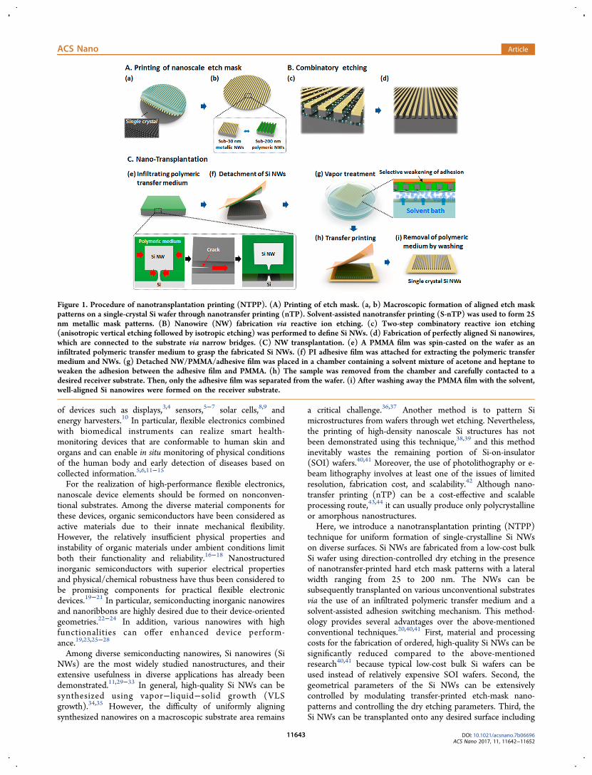
Figure 2. Fabrication of Si nanowires from a bulk Si wafer. (a) Schematic and SEM image after each step of nanowire fabrication. Scale bar:200 nm. (b−d) Fabrication of 200-nm-wide Si nanowires. (b) Top-down SEM image of printed Cr nanowires used as an etch mask. (c) Cross-section SEM images of 25 nm Si nanowires. (d) Top-down SEM images of 25 nm Si nanowires. The inset in (d) shows an optical image ofnanowires formed on the Si wafer with a size of 1.5 × 2 cm2. (e−g) Fabrication of 25-nm-wide Si nanowires. (e) Cross-section SEM images ofprinted polymeric etch mask patterns and (f) fabricated Si nanowires. (g) Plane-view SEM image showing aligned Si nanowires. The insetshows a photograph of 200-nm-wide nanowires formed on the Si wafer with a size of 1.5 × 2 cm2. (h−o) Controlling crystallographicorientations of Si NWs. (h−k) Fabrication of (100)-oriented Si nanowires. (h) Alignment of nanopatterned etch masks and ⟨100⟩ axis of Sifor fabrication of (100)-oriented Si nanowires. (i) Photograph of the printed patterns on a wafer. (j) Illustration of fabricated Si nanowires.(k) TEM image of (100)-oriented Si nanowire cross-section. Insets in (k) show the SAED pattern and HRTEM lattice image. Scale bar: 5nm−1 and 2 nm, respectively. (l−o) Fabrication of (110)-oriented Si nanowires. (l) Alignment of nanopatterned etch masks and ⟨110⟩ axis ofSi for fabrication of (110)-oriented Si nanowires. (m) Photograph of the printed patterns on a wafer. (n) Schematic image of fabricated Sinanowires. (o) TEM image of a (110)-oriented Si nanowire cross-section. Inset in (o) shows the SAED pattern and HRTEM lattice image.Scale bar: 5 nm−1 and 2 nm, respectively.
ACS Nano Article
DOI: 10.1021/acsnano.7b06696ACS Nano 2017, 11, 11642−11652
11644

nTP can generate well-defined nanopatterns on varioussubstrates by coating resist materials on an elastomeric moldhaving surface nanopatterns followed by conformal contact ofthe mold with a desired receiver substrate. It is a simple, low-cost, and large-area patterning method without the need of anycomplicated equipment such as an optical stepper. In particular,we used solvent-assisted nTP (S-nTP), which we previouslydeveloped, as a universal pattern formation method that canalso cover patterning resolution down to 10 nm43 (Figure 1b;see the Experimental Section for more details). Figure 2b and eshow scanning electron microscopy (SEM) images of printedpolymeric (poly(4-vinylpyridine); P4VP) patterns with a widthof 200 nm and metallic (Cr) patterns with a width of 25 nmserving as etch masks, respectively.For the fabrication of Si NWs, the wafers were patterned
through a reactive ion etching (RIE) process (Figure 1B). Two-step combinatorial dry etching was designed and performed (1)to precisely define the width and height of NW structures and(2) to facilitate the release of NWs from the substrate duringthe subsequent transfer printing process. For the anisotropicvertical etching, the so-called Bosch etching process (thesuccessive treatment of SF6 plasma followed by C4F8 plasma)was performed.45,46 SF6 plasma vertically etches exposed Si, andC4F8 plasma forms a polymeric fluorocarbon protection layer
on the sidewalls of NWs, suppressing lateral etching during theanisotropic etching step. Figure 2a-ii presents a cross-sectionalSEM image of a vertically etched Si wafer. For facile separationof Si NWs from the substrate, final isotropic etching with low-power SF6 plasma was performed. Because the sidewalls of SiNWs are passivated with fluorocarbon, etching of Si begins atthe bottom part of line pillars and propagates to the center.Proper control of isotropic etching time can leave a narrowbridge with a smallest width of 10−30 nm between the NWsand the substrate, which should be maintained because thecomplete separation of the Si NWs from the substrate by theRIE process degrades the alignment of NWs during subsequenttransfer. The SEM image of Figure 2a-iii shows defined Si NWsafter the completion of the lateral etching process followed byremoval of the P4VP etch mask. Also, Figure 2a-iv, c, and dexhibit low- and high-magnification SEM images of fabricatedSi NWs, which were uniformly formed over a macroscopic (20mm × 15 mm) area. The polymer etch mask was simplyremoved by a short oxygen plasma treatment or gentle washingwith an organic solvent (isopropyl alcohol, IPA).As we mentioned above, we could systematically control the
width and height of the Si NWs by modulating the width of thetransfer-printed etch mask nanopatterns and by adjusting theetch depth of the first anisotropic (vertical) etching process,
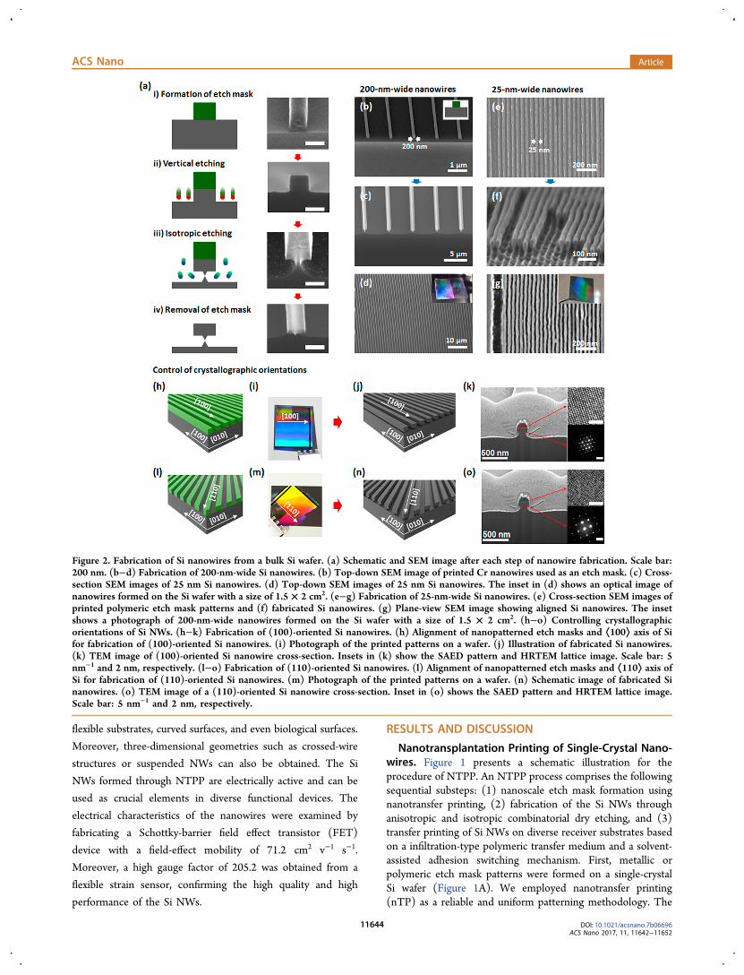
Figure 3. Transfer printing of the Si nanowires. (a) Cross-section SEM image of infiltrated polymeric transfer medium and grasping the 200-nm-wide silicon nanowires. (b) Top: Simulation result of cross-sectional stress distribution in the Si NW at 12 nm displacement with neckthickness of 100 nm (left) and 10 nm (right), respectively. Bottom: Change of von Mises stress on neck and experimentally measureddetachment yield depending on neck thickness (dashed line: fracture strength of single-crystal Si). (c) Cross-section SEM image of the waferafter detachment of the 200-nm-wide Si nanowires. (d) Photograph of detached Si nanowires from the wafer. (e) Top-down SEM image ofprinted Si nanowires. The inset shows a photograph of the transfer-printed 200-nm-wide Si nanowires. (f) Top-down SEM image of the waferafter detachment of the 25-nm-wide Si nanowires. (g) Detached 25-nm-wide Si nanowires from the wafer. (h) Top-down SEM image ofprinted 25-nm-wide Si nanowires. The inset shows a photograph of the transfer-printed 25-nm-wide Si nanowires.
ACS Nano Article
DOI: 10.1021/acsnano.7b06696ACS Nano 2017, 11, 11642−11652
11645
respectively. Although the ultimate minimum scale of printedetch mask patterns depends on the resolution of lithographictools used for the patterning of its original master template, thewidth of the printed P4VP nanopatterns of 200 nm canadditionally be reduced to 50 nm by oxygen plasma trimming,as demonstrated in Figures S1 and S2.Additionally, narrower Si NWs were formed via NTPP
(Figure 2e−g). We previously reported solvent-vapor-assistednanotransfer printing, which can form ultrafine metallicnanopatterns with even sub-10 nm resolution.43 Using S-nTP,we formed 25 nm metallic etch mask patterns. Figure 2e and fdepict SEM images of printed 25-nm-wide Cr NWs on a Siwafer and fabricated Si NWs with a width of 25 nm and heightof 30 nm, respectively. By modulating the etch depth, Si NWswith a width of 25 nm and a height of up to 180 nm werefabricated (Figure S3). Figure 2g presents a correspondinghigh-magnification SEM image and a large-area photograph offabricated NWs.We also demonstrate how NTPP provides the controllability
of crystallographic orientation of the Si NWs, which influencestheir physical properties to a great extent.33,47,48 Si wafers with aspecific crystallographic orientation were obtained using theprocess presented in Figures 2h−o. For example, we could form(100)-oriented and (110)-oriented Si NWs from the same(100) Si wafer by controlling the orientation of the long-axisdirection of the printed etch mask. Figure 2h−o illustrate large-area formation of (100)- and (110)-oriented line patterns on aSi wafer and also provide corresponding cross-section SEMimages and selected area electron diffraction (SAED) patternsof NWs after the RIE process, which clearly confirms theformation of (100)-oriented and (110)-oriented Si NWs,respectively. Cross-section transmission electron microscopy(TEM) and high-resolution TEM (HRTEM) images of Si NWare shown in the insets of Figure 2k,o and Figure S4. Thedifferent physical properties of the NWs will be discussed indetail later in this paper.For uniform and reliable transfer printing, the interfacial
fracture energy between a nanostructure and transfer medium(Gn‑m) should be higher than that between the nanostructureand the donor substrate (Gn‑d) and should be lower than thatbetween the nanostructure and the receiver substrate (Gn‑r).This constraint seriously limits the extent of applicable receiversubstrates and necessitates additional surface treatments forsubstrates that do not meet the above conditions. Previousstudies thus utilized a kinetically controlled transfer mechanismusing polydimethylsiloxane (PDMS) with low surface energy,coating of an adhesive layer on receiver substrates, or water-assisted reduction of Gn‑d.
41,49,50 However, in this work,uprooting of the SiNWs makes the process challenging dueto the physical connection of Si NWs to the mother substratevia remaining bottom linkages. Also, it is difficult to maintainthe alignment due to the shock from the neck being broken.In the final step of the NTPP process, fabricated Si NWs
were transplanted from the mother wafer onto desiredsubstrates for various applications. We thus developed anupgraded transfer printing method based on extremely robustbinding between a polymeric transfer medium and NWs and asolvent-assisted adhesion switching mechanism of polymerictransfer medium, as schematically presented in Figure 1C. First,we utilized the strategy of polymer penetration to the spacebetween the NWs and the substrate. The spin-cast polymerictransfer medium (poly(methyl methacrylate); PMMA) deeplyinfiltrates even to the region below the NWs and strongly
grasps the NWs to allow their uniform and reliable detachmentfrom the Si wafer (Figure 3a).Before detachment, we optimized the neck thickness by
controlling the duration time of isotropic dry etching based onnumerical modeling results because of the physical connectionof Si NWs to the mother substrate. For physical analysis of theneck effect, von Mises stress and cross-sectional stressdistribution simulations of the Si NWs were conducted for SiNWs with a width of 200 nm, a height of 80 nm, and a depth of120 nm, where the NWs were trapped by PMMA (Figure S5).The maximum stress was applied on the neck when the PMMAmoved upward by 12 nm (Figure 3b and Figure S5). A finiteelement method (FEM) simulation performed under theseconditions showed that as the neck became thinner, the pointof maximum stress moved from the contact point betweenPMMA and the Si NW to the narrow neck region of the SiNW. Moreover, the calculated stress applied at a neck thicknessof <50 nm was higher than the fracture strength of Si (300MPa).51 To investigate the effect of neck width on detachmentyield, we fabricated Si nanowires with neck thicknesses of 150,110, 70, and 30 nm by controlling the duration time of theisotropic dry etching process. Si NWs were not detached forneck thickness of ≥70 nm. However, a ∼100% detachmentyield was obtained for narrower necks of 30 nm. Afteroptimization of the neck thickness, the polymer film and thenanowires were homogeneously released from the wafer byattaching a polyimide (PI) adhesive film (Figure 3c, d, f, g),which can be explained by the formation and propagation ofcracks at the narrow bridges (neck).Figures 1g−i depict the mechanism and the procedure of the
solvent-assisted transfer onto the desired receiver substrates.The PI/PMMA/NWs was brought into a chamber containing asolvent mixture of acetone and heptane (5:5 volume ratio), andthe evaporated solvent molecules penetrate the polymer film.The solvent molecules existing at the interface between thepolymer film and the adhesive film weaken the adhesionbetween the polymer films due to a superlubrication effect viascreening of interfacial adhesion.43,52,53 Even though theinterfacial fracture energy (122.42 J/m2) at the interfacebetween PMMA and the adhesive film was considerably high ata dry state, it was dramatically reduced to 0.208 J/m2 whensolvent vapor was applied (Table S2). (Fracture energy wascalculated by measuring the peel strength, as shown in FigureS6.) Thus, the adhesive film can be selectively detached fromthe PMMA when the PI/PMMA/NWs was brought intocontact with a receiver surface, leaving PMMA/NWs on thereceiver substrate. Moreover, the considerably weakenedadhesion induced by the solvent-assisted adhesion switchingmechanism could overcome the limitation of the previoustransfer-printing method, which could only transfer nanostruc-tures with low interfacial fracture energy (∼2 J/m2).41,50
Consequently, extremely low fracture energy at the solvent-vapor-treated PI/PMMA interface guarantees transfer printingof the nanowires onto nearly arbitrary surfaces withoutrequiring an additional adhesive layer. After washing away thePMMA using an appropriate solvent, only the Si NWs were leftbehind on the substrate (Figure 1i).The solvent-assisted adhesion switching phenomena by the
incorporated solvent molecules enable fast, uniform, andreliable transfer of NWs while maintaining their alignmentdirection over a large area. Figure 3e and h show photographsand SEM images of transfer-printed Si NWs on a Si substrate.The photograph in Figure S7 also represents the ultralong
ACS Nano Article
DOI: 10.1021/acsnano.7b06696ACS Nano 2017, 11, 11642−11652
11646

connectivity and large-area arrangement of the printednanowires on a bending substrate. Furthermore, NTPP usingthe infiltrated polymeric transfer medium showed a markedlyimproved transfer yield compared to the conventional PDMScontact transfer printing, as shown in Figure S8a. The evaluatedtransfer yield (printed area/original area of Si NWs (width =200 nm)) of NTPP and contact printing was 98% and 34%,respectively (Figure S8b). Also, NTPP provides good align-ment quality after transfer printing. The average misalignmentangle of nanowires produced by NTPP was 1.2°, which issubstantially smaller compared to that (19.6°) of PDMS-basedtransfer printing (Figure S8c). This can be attributed to thestrong grasping capability of the infiltrated polymeric transfermedium. In addition, we also confirmed that the mother Siwafer can be recycled after using it for NTPP by surfacepolishing and cleaning processes (Figure S9), which cansignificantly reduce the material cost for the production of SiNWs.In a similar way, 25 nm Si NWs also could be produced and
transfer-printed onto diverse substrates through NTPP. Figure3f and g present the mother wafer after the detachment of Siand the photograph of detached NWs on the polymer/adhesivefilm. Figure 3h and Figure S10a and b also show high- and low-magnification SEM images of transfer-printed Si NWs with awidth of 25 nm onto a Si wafer and a PI flexible film,
respectively. The single-crystalline nature of printed nanowirescan be clearly recognized in the TEM image (Figure 2k and oand Figure S10c).
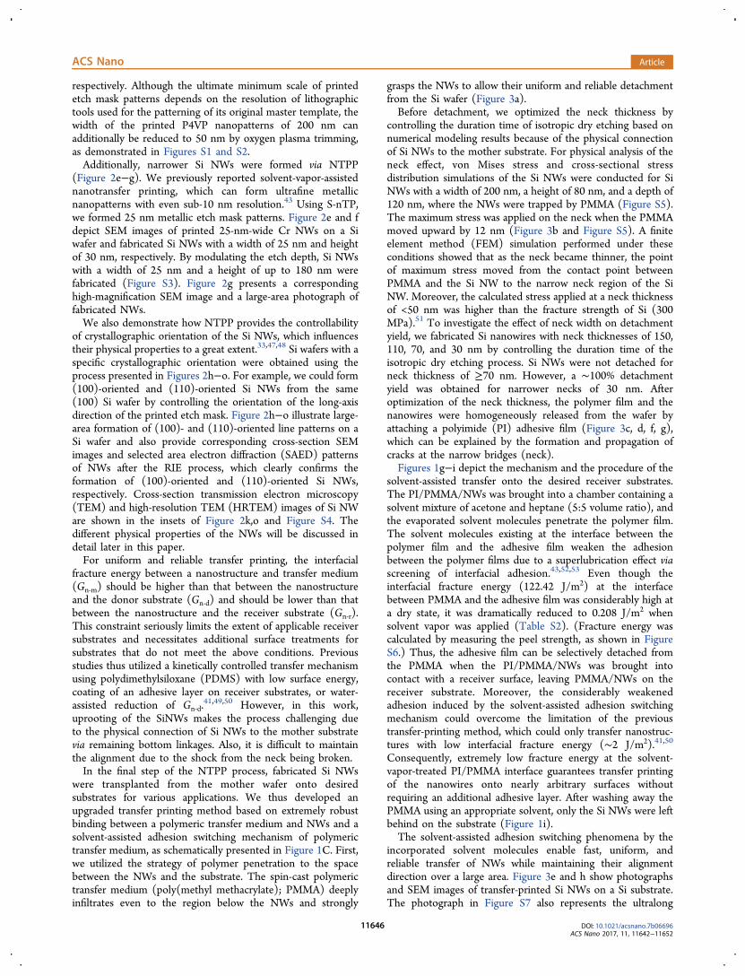
NTPP of Single-Crystal Nanowires onto DiverseSurfaces. One strong advantage of NTPP is that it does notrequire any adhesive layer or treatment on receiver substrates,and thus it allows printing on nearly arbitrary surfacesregardless of surface chemistry and topography. As an example,the formation of inorganic semiconductors on biologicalsurfaces such as human skin can contribute to the realizationof future biomedical electronics such as electronic skin andhealth-care monitoring devices. As schematically illustrated inFigure 4a, Si NWs were successfully printed on the surface ofhuman skin (Figure 4b). These printed NWs on skin would beable to directly collect biosignals.Additionally, the fabrication of three-dimensional (3D)
complex structures was also realized by implementing NTPPmultiple times on the same receiver substrates. As ademonstration of three-dimensional nanostructures, we fab-ricated simple crossed-wire structures through sequentialprinting of Si NW arrays (Figure 4c,d). First, we transfer-printed a first layer of Si NWs, and after removal of the PMMAtransfer medium, a second layer of Si NWs was printed whilearranging the angle between the upper and lower nanowires at90°. The low- and high-magnification SEM images in Figure 4d
Figure 4. Printing of Si nanowires on unusual surfaces and fabrication of three-dimensional structures. (a, b) NTPP applied to biologicalsurfaces. (a) Schematic procedure of printing Si nanowires on nonplanar surfaces. (b) Photograph of Si nanowires printed on human skin. (c,d) Fabrication of three-dimensional structures. (c) Fabrication procedure and (d) SEM image of a crossed Si nanowire structure. (e, f)Fabrication of suspended-Si-nanowire structures. (e) Schematic of fabrication of a suspended nanowire structure. (f) Top-down SEM image ofsuspended nanowire structure.
ACS Nano Article
DOI: 10.1021/acsnano.7b06696ACS Nano 2017, 11, 11642−11652
11647

were obtained after removal of the PMMA medium. Successiveprinting of Si NWs can generate even more complex 3Dstructures, and such three-dimensional periodic nanostructurescan be useful for diverse applications including photoniccrystals, metamaterials, and sensors.The adhesion switching effect makes it possible to print
nanostructures on topographically modulated surfaces, whereonly a minimum contact area between donor and receiversubstrates exists. We successfully fabricated suspended NWstructures on a deep trench substrate, as shown in Figure 4e. Tofabricate suspended nanowire structures, a PMMA/NWs wascarefully laid on a supporting deep trench structure with adepth of 1 μm and a width of 50 μm. Toluene vapor was thenapplied to the PMMA transfer medium by proximallyapproaching a toluene-saturated PDMS gel pad, which wasprepared by dipping a dry PDMS pad in a toluene bath for 6 h.After removing the PMMA film by dipping the whole deviceinto a solvent bath (toluene), suspended nanowire structureswere successfully obtained (Figure 4f). These suspendednanowire structures can be particularly useful for high-performance nanosensors with a high sensitivity because allthe surface areas can be exposed to analytes. In addition,suspended or free-standing semiconducting nanowires can beexploited to realize emerging biomedical applications such asintracellular recording54 and cell endoscopy28 based on free-standing nanowires attached to optical fibers.
Electrical Characterization and Demonstration of aFlexible Strain Sensor. For the electrical characterization ofprinted NWs, we fabricated a Schottky-barrier FET, where theNWs function as an active channel (Figure 5A). In a Schottky-barrier FET, junctions are formed between the semiconductorand the source/drain metal electrode. To prepare the FETdevice shown in Figure 5a, we transfer-printed Si NWs on aheavily doped p-type Si wafer with a thermally grown oxidelayer (thickness = 300 nm). It is well known that the electricalresponse of the Schottky-barrier FET varies depending on thework functions of the electrode and the semiconductor. Weformed a Ti/Au electrode on two sides of the Si NWs andannealed the sample at 600 °C for 5 min in a vacuum systemusing rapid thermal annealing equipment to form a Schottkyjunction. Figure S11a shows an SEM image captured from thecentral region of the fabricated device.Electrical characterization of the 200-nm-wide p-type Si-NW
FET device was then performed. Figure 5b (Ids−Vgs curves ofthe device) clearly shows the switching of the device with anon−off current ratio of nearly 104 at a Vds of 1 V, and the field-effect hole mobility was calculated to be 71.2 cm2 v−1 s−1. Theelectrical performance of our device upon the application ofgate bias is consistent with that of a previously reported FETdevice with a Ti/Au electrode and p-type Si NWs.30 Similarly,we also fabricated a FET device with 25-nm-wide NWs usingan n-type Si wafer (resistivity = 1 Ω·cm). Figures 5c and S11bshow the obtained Ids−Vgs curve and Id vs Vd curve of the device
Figure 5. Device applications of Si NWs. (A) Electrical characterization of Si NWs. (a) Schematic showing the structure of a nanowire-basedFET device. (b) Drain current (Id) vs gate bias (Vg) characteristics for 200-nm-wide Si (p-type) nanowires. (c) Id vs Vg characteristics of 25-nm-wide Si (n-type) nanowires. (B) Demonstration of a flexible strain sensor. (d) Conceptual drawing of the strain sensor. (e) Change of ΔR/Ro and gauge factor depending on strain. (f) Cycling test of the strain sensor device. (ΔR/Ro was repeatedly measured for 50 strain cycles.)
ACS Nano Article
DOI: 10.1021/acsnano.7b06696ACS Nano 2017, 11, 11642−11652
11648

and the field-effect mobility of electrons of 1.6 cm2 v−1 s−1. Thesignificantly reduced mobility of small-diameter nanowires canbe attributed to the contribution of surface defects and trapsites from surface roughness.30,55−57 Because the mobility of afield-effect transistor highly depends on the fabricationconditions, we expect that the mobility can be even furtherenhanced through optimization of the fabrication process, forexample, by decreasing the doping level or minimizing thetrapping states on the nanowire surface.30,57
The possibility of an ultrasensitive piezoresistive strain sensorusing Si NWs has been suggested.33,58,59 For example, Yang etal. experimentally demonstrated giant piezoresistance of SiNWs with a diameter of 50−300 nm.33 In addition, the highlyflexible nature of Si NWs can be utilized to realize a high-performance strain sensor, which can be easily mounted ontodiverse surfaces. However, as mentioned above, vapor- orsolution-phase synthesis and rearrangement of NWs canaccompany technical issues such as large variation of thephysical response and reproducibility.We demonstrate how the NTPP process can be used for the
fabrication of high-performance NW strain sensors in a simpleand reliable way (Figure 5B). First, using NTPP, well-defined SiNWs were formed on a flat PDMS pad as a stretchablesubstrate. The longitudinal crystallographic orientation of thenanowires was carefully controlled to be (100) or (110), wherethe (110) orientation was reported to have a strongerpiezoresistive effect.33 A metal electrode was then definedthrough thermal evaporation of Ag in the presence of a shadowmask (Figure S12a). For characterization, the strain sensor wasmounted on a measurement device, as shown in Figures 5d andS12b. The resistance of the device was monitored with varyingunidirectional tensile strain. The graph in Figures 5e depicts thechange of the relative resistance (ΔR/Ro) as a function of theapplied tensile strain (ε).The gauge factor (GF), which is defined as (ΔR/Ro)/ε, was
used as a measure of sensitivity. The (110)-oriented Si NWsensor recorded a GF of 205.2 (±7.4) in the applied strainrange of 0−5%. The measured GF of our device was 30 timeshigher than the previously reported gauge factor of a strainsensor made of transfer-printed Si NWs.58 In contrast, thedevice with (100)-oriented Si NWs shows a GF of 14.9 (±2.3)in the strain range of 0−5%, which is consistent with previousreports,58 suggesting the importance of orientation controll-ability for maximizing the piezoresistive effect. The abruptincrease of resistance over 5% of strain can be attributed to thepartial breakage of Si NWs.60 However, it is worthwhile to notethat even a large strain of 12% did not completely break theNWs, as shown in Figure S12c, implying the outstandingflexibility of our NWs. We also performed a cycling test (at astrain of 1.5%) to investigate whether the piezoresistive effect of(110)-oriented Si NWs is reversible. With repeated applicationand removal of strain, ΔR/Ro changed reversibly and reliablyover 50 times, as shown in Figure 5f. The standard deviation ofΔR/Ro at the 1.5% strained state was approximately 10%.
CONCLUSIONIn summary, we introduced a highly facile and reliable strategyof nanotransplantation printing to form high-quality, long-range-ordered single-crystalline nanostructures on arbitrarysubstrates. After printing nanoscale etch mask patterns with awidth of 25−200 nm on a single-crystal Si wafer, a combinatoryreactive ion etching process composed of anisotropic andisotropic etching generates Si NWs connected to the substrate
via narrow bridges with extensive control of the geometricalparameters of the NWs. A polymeric transfer mediuminfiltrated the nanoscale gap between defined NWs and themother Si substrate leads to tight binding of the NWs in thepolymer transfer medium, which enables uniform detachmentof an array of the NWs from the substrate via homogeneousbreakage of the narrow bridges. Dynamic adhesion switching bysolvent vapor exposure facilitates rapid and efficient transferprinting of the single-crystalline NWs onto diverse substratesincluding flexible and biological surfaces without the need ofany surface treatment, leading to an extremely high transferyield of 96%. The electrical characteristics (field effect mobilityof 71.2 cm2 v−1 s−1) of the nanowires were confirmed byfabricating and characterizing a high-performance Schottky-barrier field-effect transistor and piezoresistive strain sensordevices. In particular, the controllability of crystallographicorientation results in a large gauge factor of over 205.2 for the(110) orientation. This concept of the NTPP process can beapplied not only for Si NWs but also for various high-qualitysingle-crystal semiconducting nanowires, and we expect thatthese nanostructures can be highly useful for various high-performance future nanodevices formed on arbitrary surfaces.
EXPERIMENTAL SECTIONFabrication of 200 nm Scale Master Mold. The Si master
template was fabricated using KrF photolithography followed byreactive ion etching. A positive photoresist (PR, Dongjin SemichemCo. Ltd.) with a thickness of 400 nm was spin-coated and thenexposed using a KrF scanner (Nikon, NSR-S203B), followed bydeveloping using a developer solution (tetramethylammoniumhydroxide, Dongjin Semichem Co.Ltd.). The PR patterns were usedas an etch mask to pattern the Si surface by reactive ion etching (gas:CF4, working pressure: 7 mTorr, plasma power: 250 W). The Simaster templates were 200 nm in width and 350 nm in height with a1.2 μm period.
Fabrication of 25 nm Master Mold. Directed self-assembly ofpolystyrene-b-polydimethylsiloxane (PS-b-PDMS) block copolymer(BCP) has been previously studied to create ordered patterns61,62 andvarious applications.63−66 We thus employed this technique for large-area preparation of a high-resolution master mold.67−69 PS-b-PDMSBCP with a MW of 48 kg mol−1 (SD48), which forms 25-nm-widelines, respectively, was purchased from Polymer Source Inc. and usedwithout purification. SD48 BCP was dissolved in a mixed solvent oftoluene, heptane, and propylene glycol monomethyl ether acetate(1:1:1 by volume), yielding a 1.0 wt % polymer solution. Surface-patterned Si substrates with a width of 1 μm, a depth of 40 nm, and aperiod of 1.25 μm were used as guiding templates. The substrate wastreated with a PDMS brush (5 kg mol−1, Polymer Source Inc.) at 150°C using a vacuum oven. A solution of SD48 was spin-cast onto thetemplate and annealed for 6 h in the chamber at room temperatureusing toluene vapor. In order to remove the top-segregated PDMSlayer and organic block (PS), the samples were etched by CF4 plasma(etching time 20 s, gas flow rate 30 sccm, working pressure 15 mTorr,and plasma source power 50 W) followed by O2 plasma (etching time30 s, gas flow rate 30 sccm, working pressure 15 mTorr, and plasmasource power 60 W).
Formation of Polymeric Etch Mask Patterns on a Si Wafer.Surface patterns of the Si master template were 200 nm in width and350 nm in height with a 1.2 μm period. Prior to the replication, thesurface of the master template was treated with an OH-terminatedPDMS brush (molecular weight (MW) = 5 kg mol−1, Polymer SourceInc.). By retracting the cured PDMS from the template, surfacepatterns of the template were securely replicated on the mold. Poly(4-vinylpyridine) (MW = 60 kg mol−1, Sigma-Aldrich Inc.) was dissolvedin a mixture of IPA and acetone (1:1 by weight), to yield a 4 wt %solution. P4VP thin film was then spin-casted on the elastomericPDMS stamp to replicate the surface patterns of the mold. Through
ACS Nano Article
DOI: 10.1021/acsnano.7b06696ACS Nano 2017, 11, 11642−11652
11649

the conformal contact of the PDMS stamp with a single-crystal Siwafer, the patterned P4VP film was securely transferred on the wafer.After short treatment of oxygen plasma (gas flow rate = 30 sccm,working pressure = 15 mTorr, plasma source power = 100 W, and biaspower 60 W), the residual bottom polymer layers were removed, and200-nm-wide nanopatterns with a 1.2 μm period were formed with ahigh uniformity over a large area (20 mm × 15 mm).Formation of 25 nm Metallic Etch Mask Patterns on a Si
Wafer. Prior to the replication, the surface of the master mold wastreated with a PDMS brush (Polymer Source Inc.). PMMA (MW =100 kg/mol, Sigma-Aldrich Inc.) was dissolved in a mixture of acetone,toluene, and heptane (4.5:4.5:1), yielding 4 wt % solutions. PMMAfilm was spin-casted on the master mold. A polyimide adhesive film(3M Inc.) was then attached on the surface of the bilayer polymerreplica. By retracting the adhesive film from the mold, the replica withthe inverted image of its surface topography was detached from themold. Cr nanowires were formed through glancing-angle deposition ofCr onto the polymer replica using an e-beam evaporator. Toluenevapor was then applied to the polymer replica film by placing thereplica/adhesive film into a solvent-saturated chamber, which waspreheated to 45 °C. After 30 s, the adhesive film was taken out fromthe chamber and brought into contact with the Si substrate. Theadhesive film was then selectively detached from the substrate.Uniformly arranged Cr nanowire etch mask patterns on a Si substratecan then be obtained by washing away the polymer replica film usingan appropriate solvent.Fabrication of Si Nanowires through a Two-Step Etching
Process. For the anisotropic vertical etching, the successive treatmentof SF6 plasma treatment (gas flow rate = 30 sccm, working pressure =15 mTorr, plasma source power = 110 W, and bias power 60 W)followed by C4F8 plasma treatment (gas flow rate = 30 sccm, workingpressure = 15 mTorr, plasma source power = 100 W, and bias power40 W) was repeated. Importantly, the number of repetitions definesthe depth of vertical etching and the height of the nanowires. For thefinal horizontal etching, low-power SF6 plasma treatment (gas flowrate = 30 sccm, working pressure = 15 mTorr, plasma source power =50 W, and bias power 10 W) was performed.Fabrication and Characterization of Schottky-Junction
Field-Effect Transistor. Si NWs were transfer-printed on a Siwafer heavily doped with boron (resistivity <0.005 Ω cm) with athermally grown oxide layer (300 nm). Back-gated Si NW FETs werefabricated using conventional photolithoraphy. To pattern the sourceand drain electrodes, a photoresist (AZ5142E) and a mask aligner(MDA-8000B) were used followed by a development process usingAZ300MIF developer. An electrode with Ni (20 nm)/Au (200 nm)was deposited by electron beam evaporation followed by a lift-offprocess with AZ400T. Finally, the fabricated FETs were annealed in atube furnace for 1 h (Ar/4% H2, 200 °C) to enhance the contactproperty. Electrical characterization of Si NW FETs was carried outusing a Keithley 4200-SCS and a probe station in ambient conditions.The transfer characteristics were measured with sweeping Vgs from−150 to 150 V with a step size of 0.5 V. The carrier mobility (μ) of thesamples was obtained from μ = (dIds/dVgs)(L/WCgVds), where L is thechannel length and W is the channel width. L and W were obtainedfrom SEM images. The back-gate capacitance (Cg) for 300-nm-thickSiO2 was 1.151 × 10⁻⁴ F·m−2 (Ci = ε0εr/d, ε0 = 8.85 × 10⁻¹² F·m−1, εr= 3.9, d = 300 nm), which was calculated by assuming a parallel-platecapacitance model.30,70
Fabrication and Characterization of Piezoresistive NanowireStrain Sensor. Prepolymers and curing agent (Sylgard 184, DowCorning Co. Ltd.) were mixed with a weight ratio of 10:1, and theresultant air bubbles in the mixture were eliminated by degassingunder vacuum. The mixture was then poured onto a chalet and bakedat 150 °C for 30 min using a convection oven. The prepared PDMSsamples were cut by scissors with a size of 15 mm × 60 mm. Si NWswere transplanted onto the PDMS pad. Ag electrodes (500 nm) werethen deposited on top of the nanowire arrays via thermal evaporation.Two rectangular 5 mm × 5 mm Ag electrodes with a 50 μm gap werefabricated using a stainless-steel shadow mask.
SEM and TEM Characterization. For the observation andanalysis of the samples, a field emission scanning electron microscope(FE-SEM, Hitachi S-4800) with an acceleration voltage of 10 kV and aworking distance of 5 mm was used. Field emission TEM (Tecnai G2F30 S-Twin, FEI, acceleration voltage of 300 kV) was also used toconfirm the crystallinity and orientation of the Si NWs.
FEM Simulation Method for Modeling Neck Stress Dis-tribution. A FEM simulation was conducted using ABAQUS (v6.14).The model geometries were created in a 2D deformable solid with theelement type CPS4R, which is a four-node bilinear plane stressquadrilateral, reduced integration, and hourglass control. The staticgeneral procedure was used. To apply the loading condition to thespecimen, the Si nanowire was fixed on the ground and the PMMAwas pulled off the nanowire by moving it upward. The materialproperties of Si and PMMA are listed in Table S1.
ASSOCIATED CONTENT*S Supporting InformationThe Supporting Information is available free of charge on theACS Publications website at DOI: 10.1021/acsnano.7b06696.
Supplementary figures and tables (PDF)
AUTHOR INFORMATIONCorresponding Author*E-mail: [email protected] Yoon: 0000-0002-9447-3807Taek-Soo Kim: 0000-0002-2825-7778Yeon Sik Jung: 0000-0002-7709-8347Author Contributions¶H. J. Han and J. W. Jeong contributed equally to this work.NotesThe authors declare no competing financial interest.
ACKNOWLEDGMENTSThis research was supported by the Creative MaterialsDiscovery Program through the National Research Foundationof Korea (NRF) funded by the Ministry of Science, ICT andFuture Planning (NRF-2016M3D1A1900035). This work wasalso supported by a National Research Foundation of Korea(NRF) grant funded by the Korean government (MSIP)(NRF-2017R1A2B2009948). This work was also partiallysupported by Open Innovation Lab Project from NationalNanofab Center (NNFC).
REFERENCES(1) Nathan, A.; Ahnood, A.; Cole, M. T.; Lee, S.; Suzuki, Y.; Hiralal,P.; Bonaccorso, F.; Hasan, T.; Garcia-Gancedo, L.; Dyadyusha, A.;Haque, S.; Andrew, P.; Hofmann, S.; Moultrie, J.; Chu, D. P.; Flewitt,A. J.; Ferrari, A. C.; Kelly, M. J.; Robertson, J.; Amaratunga, G. A. J.;Milne, W. I. Flexible Electronics: The Next Ubiquitous Platform. Proc.IEEE 2012, 100, 1486−1517.(2) Boland, J. J. Flexible Electronics: Within Touch of Artificial Skin.Nat. Mater. 2010, 9, 790−792.(3) Kim, R.-H.; Kim, D.-H.; Xiao, J.; Kim, B. H.; Park, S.-I.; Panilaitis,B.; Ghaffari, R.; Yao, J.; Li, M.; Liu, Z. Waterproof AlInGaPOptoelectronics on Stretchable Substrates with Applications inBiomedicine and Robotics. Nat. Mater. 2010, 9, 929.(4) White, M. S.; Kaltenbrunner, M.; Głowacki, E. D.; Gutnichenko,K.; Kettlgruber, G.; Graz, I.; Aazou, S.; Ulbricht, C.; Egbe, D. A.;Miron, M. C. Ultrathin, Highly Flexible and Stretchable PLEDs. Nat.Photonics 2013, 7, 811−816.(5) Kim, D. H.; Lu, N. S.; Ma, R.; Kim, Y. S.; Kim, R. H.; Wang, S.D.; Wu, J.; Won, S. M.; Tao, H.; Islam, A.; Yu, K. J.; Kim, T. I.;
ACS Nano Article
DOI: 10.1021/acsnano.7b06696ACS Nano 2017, 11, 11642−11652
11650

Chowdhury, R.; Ying, M.; Xu, L. Z.; Li, M.; Chung, H. J.; Keum, H.;McCormick, M.; Liu, P.; Zhang, Y. W.; Omenetto, F. G.; Huang, Y. G.;Coleman, T.; Rogers, J. A. Epidermal Electronics. Science 2011, 333,838−843.(6) Son, D.; Lee, J.; Qiao, S.; Ghaffari, R.; Kim, J.; Lee, J. E.; Song, C.;Kim, S. J.; Lee, D. J.; Jun, S. W.; Yang, S.; Park, M.; Shin, J.; Do, K.;Lee, M.; Kang, K.; Hwang, C. S.; Lu, N. S.; Hyeon, T.; Kim, D. H.Multifunctional Wearable Devices for Diagnosis and Therapy ofMovement Disorders. Nat. Nanotechnol. 2014, 9, 397−404.(7) Yu, S.; Han, H. J.; Kim, J. M.; Yim, S.; Sim, D. M.; Lim, H.; Lee, J.H.; Park, W. I.; Park, J. H.; Kim, K. H. Area-Selective Lift-OffMechanism Based on Dual-Triggered Interfacial Adhesion Switching:Highly Facile Fabrication of Flexible Nanomesh Electrode. ACS Nano2017, 11, 3506−3516.(8) Lee, J.; Wu, J.; Shi, M.; Yoon, J.; Park, S. I.; Li, M.; Liu, Z.;Huang, Y.; Rogers, J. A. Stretchable GaAs Photovoltaics with DesignsThat Enable High Areal Coverage. Adv. Mater. (Weinheim, Ger.) 2011,23, 986−991.(9) Kaltenbrunner, M.; White, M. S.; Głowacki, E. D.; Sekitani, T.;Someya, T.; Sariciftci, N. S.; Bauer, S. Ultrathin and LightweightOrganic Solar Cells with High Flexibility. Nat. Commun. 2012, 3, 770.(10) Anderson, I. A.; Gisby, T. A.; McKay, T. G.; O’Brien, B. M.;Calius, E. P. Multi-Functional Dielectric Elastomer Artificial Musclesfor Soft and Smart Machines. J. Appl. Phys. (Melville, NY, U. S.) 2012,112, 041101.(11) Webb, R. C.; Bonifas, A. P.; Behnaz, A.; Zhang, Y. H.; Yu, K. J.;Cheng, H. Y.; Shi, M. X.; Bian, Z. G.; Liu, Z. J.; Kim, Y. S.; Yeo, W. H.;Park, J. S.; Song, J. Z.; Li, Y. H.; Huang, Y. G.; Gorbach, A. M.; Rogers,J. A. Ultrathin Conformal Devices for Precise and ContinuousThermal Characterization of Human Skin. Nat. Mater. 2013, 12, 938−944.(12) Bauer, S. Flexible Electronics Sophisticated Skin. Nat. Mater.2013, 12, 871−872.(13) Jeong, J. W.; Yeo, W. H.; Akhtar, A.; Norton, J. J. S.; Kwack, Y.J.; Li, S.; Jung, S. Y.; Su, Y. W.; Lee, W.; Xia, J.; Cheng, H. Y.; Huang,Y. G.; Choi, W. S.; Bretl, T.; Rogers, J. A. Materials and OptimizedDesigns for Human-Machine Interfaces via Epidermal Electronics.Adv. Mater. (Weinheim, Ger.) 2013, 25, 6839−6846.(14) Wang, X. W.; Gu, Y.; Xiong, Z. P.; Cui, Z.; Zhang, T. Silk-Molded Flexible, Ultrasensitive, and Highly Stable Electronic Skin forMonitoring Human Physiological Signals. Adv. Mater. (Weinheim, Ger.)2014, 26, 1336−1342.(15) Xu, S.; Zhang, Y. H.; Jia, L.; Mathewson, K. E.; Jang, K. I.; Kim,J.; Fu, H. R.; Huang, X.; Chava, P.; Wang, R. H.; Bhole, S.; Wang, L.Z.; Na, Y. J.; Guan, Y.; Flavin, M.; Han, Z. S.; Huang, Y. G.; Rogers, J.A. Soft Microfluidic Assemblies of Sensors, Circuits, and Radios for theSkin. Science 2014, 344, 70−74.(16) Kaltenbrunner, M.; Sekitani, T.; Reeder, J.; Yokota, T.; Kuribara,K.; Tokuhara, T.; Drack, M.; Schwodiauer, R.; Graz, I.; Bauer-Gogonea, S.; Bauer, S.; Someya, T. An Ultra-Lightweight Design forImperceptible Plastic Electronics. Nature 2013, 499, 458−463.(17) Sekitani, T.; Zschieschang, U.; Klauk, H.; Someya, T. FlexibleOrganic Transistors and Circuits with Extreme Bending Stability. Nat.Mater. 2010, 9, 1015−1022.(18) Zirkl, M.; Haase, A.; Fian, A.; Schon, H.; Sommer, C.; Jakopic,G.; Leising, G.; Stadlober, B.; Graz, I.; Gaar, N.; Schwodiauer, R.;Bauer-Gogonea, S.; Bauer, S. Low-Voltage Organic Thin-FilmTransistors with High-k Nanocomposite Gate Dielectrics for FlexibleElectronics and Optothermal Sensors. Adv. Mater. (Weinheim, Ger.)2007, 19, 2241−2245.(19) McAlpine, M. C.; Ahmad, H.; Wang, D. W.; Heath, J. R. HighlyOrdered Nanowire Arrays on Plastic Substrates for UltrasensitiveFlexible Chemical Sensors. Nat. Mater. 2007, 6, 379−384.(20) Ahn, J. H.; Kim, H. S.; Lee, K. J.; Jeon, S.; Kang, S. J.; Sun, Y. G.;Nuzzo, R. G.; Rogers, J. A. Heterogeneous Three-DimensionalElectronics by Use of Printed Semiconductor Nanomaterials. Science2006, 314, 1754−1757.(21) Kim, D. H.; Lu, N. S.; Ghaffari, R.; Rogers, J. A. InorganicSemiconductor Nanomaterials for Flexible and Stretchable Bio-
Integrated Electronics. NPG Asia Mater. 2012, 4.e1510.1038/am.2012.27(22) Baca, A. J.; Ahn, J. H.; Sun, Y. G.; Meitl, M. A.; Menard, E.; Kim,H. S.; Choi, W. M.; Kim, D. H.; Huang, Y.; Rogers, J. A.Semiconductor Wires and Ribbons for High-Performance FlexibleElectronics. Angew. Chem., Int. Ed. 2008, 47, 5524−5542.(23) Liu, X.; Long, Y. Z.; Liao, L.; Duan, X. F.; Fan, Z. Y. Large-ScaleIntegration of Semiconductor Nanowires for High-PerformanceFlexible Electronics. ACS Nano 2012, 6, 1888−1900.(24) Xia, Y. N.; Yang, P. D.; Sun, Y. G.; Wu, Y. Y.; Mayers, B.; Gates,B.; Yin, Y. D.; Kim, F.; Yan, Y. Q. One-Dimensional Nanostructures:Synthesis, Characterization, and Applications. Adv. Mater. (Weinheim,Ger.) 2003, 15, 353−389.(25) Yang, P. D.; Yan, R. X.; Fardy, M. Semiconductor Nanowire:What’s Next? Nano Lett. 2010, 10, 1529−1536.(26) Zhai, T. Y.; Fang, X. S.; Li, L.; Bando, Y.; Golberg, D. One-Dimensional CdS Nanostructures: Synthesis, Properties, and Applica-tions. Nanoscale 2010, 2, 168−187.(27) Patolsky, F.; Lieber, C. M. Nanowire Nanosensors. Mater. Today2005, 8, 20−28.(28) Yan, R. X.; Gargas, D.; Yang, P. D. Nanowire Photonics. Nat.Photonics 2009, 3, 569−576.(29) Boukai, A. I.; Bunimovich, Y.; Tahir-Kheli, J.; Yu, J. K.; Goddard,W. A.; Heath, J. R. Silicon Nanowires as Efficient ThermoelectricMaterials. Nature 2008, 451, 168−171.(30) Cui, Y.; Zhong, Z. H.; Wang, D. L.; Wang, W. U.; Lieber, C. M.High Performance Silicon Nanowire Field Effect Transistors. NanoLett. 2003, 3, 149−152.(31) Chan, C. K.; Peng, H. L.; Liu, G.; McIlwrath, K.; Zhang, X. F.;Huggins, R. A.; Cui, Y. High-Performance Lithium Battery AnodesUsing Silicon Nanowires. Nat. Nanotechnol. 2008, 3, 31−35.(32) Hochbaum, A. I.; Chen, R. K.; Delgado, R. D.; Liang, W. J.;Garnett, E. C.; Najarian, M.; Majumdar, A.; Yang, P. D. EnhancedThermoelectric Performance of Rough Silicon Nanowires. Nature2008, 451, 163−165.(33) He, R. R.; Yang, P. D. Giant Piezoresistance Effect in SiliconNanowires. Nat. Nanotechnol. 2006, 1, 42−46.(34) Hochbaum, A. I.; Fan, R.; He, R. R.; Yang, P. D. ControlledGrowth of Si Nanowire Arrays for Device Integration. Nano Lett.2005, 5, 457−460.(35) Fan, H. J.; Werner, P.; Zacharias, M. Semiconductor Nanowires:From Self-Organization to Patterned Growth. Small 2006, 2, 700−717.(36) Wang, M. C. P.; Gates, B. D. Directed Assembly of Nanowires.Mater. Today 2009, 12, 34−43.(37) Sun, Y. G.; Rogers, J. A. Inorganic Semiconductors for FlexibleElectronics. Adv. Mater. (Weinheim, Ger.) 2007, 19, 1897−1916.(38) Ko, H. C.; Baca, A. J.; Rogers, J. A. Bulk Quantities of Single-Crystal Silicon Micro-/Nanoribbons Generated from Bulk Wafers.Nano Lett. 2006, 6, 2318−2324.(39) Baca, A. J.; Meitl, M. A.; Ko, H. C.; Mack, S.; Kim, H. S.; Dong,J. Y.; Ferreira, P. M.; Rogers, J. A. Printable Single-Crystal SiliconMicro/Nanoscale Ribbons, Platelets and Bars Generated from BulkWafers. Adv. Funct. Mater. 2007, 17, 3051−3062.(40) Khang, D. Y.; Jiang, H. Q.; Huang, Y.; Rogers, J. A. AStretchable Form of Single-Crystal Silicon for High-PerformanceElectronics on Rubber Substrates. Science 2006, 311, 208−212.(41) Meitl, M. A.; Zhu, Z. T.; Kumar, V.; Lee, K. J.; Feng, X.; Huang,Y. Y.; Adesida, I.; Nuzzo, R. G.; Rogers, J. A. Transfer Printing byKinetic Control of Adhesion to an Elastomeric Stamp. Nat. Mater.2006, 5, 33−38.(42) Fontana, R. E.; Katine, J.; Rooks, M.; Viswanathan, R.; Lille, J.;MacDonald, S.; Kratschmer, E.; Tsang, C.; Nguyen, S.; Robertson, N.;Kasiraj, P. E-beam Writing: A Next-Generation Lithography Approachfor Thin-Film Head Critical Features. IEEE Trans. Magn. 2002, 38,95−100.(43) Jeong, J. W.; Yang, S. R.; Hur, Y. H.; Kim, S. W.; Baek, K. M.;Yim, S.; Jang, H. I.; Park, J. H.; Lee, S. Y.; Park, C. O.; Jung, Y. S. High-
ACS Nano Article
DOI: 10.1021/acsnano.7b06696ACS Nano 2017, 11, 11642−11652
11651

Resolution Nanotransfer Printing Applicable to Diverse Surfaces viaInterface-Targeted Adhesion Switching. Nat. Commun. 2014, 5, 5387.(44) Seo, M. H.; Yoo, J. Y.; Choi, S. Y.; Lee, J. S.; Choi, K. W.; Jeong,C. K.; Lee, K. J.; Yoon, J. B. Versatile Transfer of an Ultralong andSeamless Nanowire Array Crystallized at High Temperature for Use inHigh-Performance Flexible Devices. ACS Nano 2017, 11, 1520−1529.(45) Gao, F.; Ylinen, S.; Kainlauri, M.; Kapulainen, M. SmoothSilicon Sidewall Etching for Waveguide Structures Using a ModifiedBosch Process. J. Micro/Nanolithogr., MEMS, MOEMS 2014, 13,013010−013010.(46) Laermer, F.; Schilp, A. Method of Anisotropically EtchingSilicon. U.S. Patent 5501893A, Mar 26, 1996.(47) Barwicz, T.; Klein, L.; Koester, S. J.; Hamann, H. SiliconNanowire Piezoresistance: Impact of Surface CrystallographicOrientation. Appl. Phys. Lett. 2010, 97, 02311010.1063/1.3463456.(48) Kanda, Y. Piezoresistance Effect of Silicon. Sens. Actuators, A1991, 28, 83−91.(49) Feng, X.; Meitl, M. A.; Bowen, A. M.; Huang, Y.; Nuzzo, R. G.;Rogers, J. A. Competing Fracture in Kinetically Controlled TransferPrinting. Langmuir 2007, 23, 12555−12560.(50) Carlson, A.; Bowen, A. M.; Huang, Y.; Nuzzo, R. G.; Rogers, J.A. Transfer Printing Techniques for Materials Assembly and Micro/Nanodevice Fabrication. Adv. Mater. (Weinheim, Ger.) 2012, 24,5284−5318.(51) Pramanik, C.; Saha, H.; Gangopadhyay, U. Design Optimizationof a High Performance Silicon MEMS Piezoresistive Pressure Sensorfor Biomedical Applications. J. Micromech. Microeng. 2006, 16, 2060.(52) Nomura, A.; Ohno, K.; Fukuda, T.; Sato, T.; Tsujii, Y.Lubrication Mechanism of Concentrated Polymer Brushes in Solvents:Effect of Solvent Viscosity. Polym. Chem. 2012, 3, 148−153.(53) Nomura, A.; Okayasu, K.; Ohno, K.; Fukuda, T.; Tsujii, Y.Lubrication Mechanism of Concentrated Polymer Brushes in Solvents:Effect of Solvent Quality and Thereby Swelling State. Macromolecules2011, 44, 5013−5019.(54) Qing, Q.; Jiang, Z.; Xu, L.; Gao, R.; Mai, L.; Lieber, C. M. Free-standing Kinked Nanowire Transistor Probes for Targeted Intra-cellular Recording in Three Dimensions. Nat. Nanotechnol. 2014, 9,142−147.(55) Wolf, S. Silicon Processing for the VLSI Era. LATTICE 1995,559−581.(56) Poli, S.; Pala, M. G.; Poiroux, T.; Deleonibus, S.; Baccarani, G.Size Dependence of Surface-Roughness-Limited Mobility in Silicon-Nanowire FETs. IEEE Trans. Electron Devices 2008, 55, 2968−2976.(57) Cui, Y.; Duan, X. F.; Hu, J. T.; Lieber, C. M. Doping andElectrical Transport in Silicon Nanowires. J. Phys. Chem. B 2000, 104,5213−5216.(58) Ryu, S. Y.; Xiao, J.; Park, W. I.; Son, K. S.; Huang, Y. Y.; Paik,U.; Rogers, J. A. Lateral Buckling Mechanics in Silicon Nanowires onElastomeric Substrates. Nano Lett. 2009, 9, 3214−3219.(59) Koumela, A.; Mercier, D.; Dupre, C.; Jourdan, G.; Marcoux, C.;Ollier, E.; Purcell, S. T.; Duraffourg, L. Piezoresistance of Top-DownSuspended Si Nanowires. Nanotechnology 2011, 22.39570110.1088/0957-4484/22/39/395701(60) Zhu, Y.; Xu, F.; Qin, Q. Q.; Fung, W. Y.; Lu, W. MechanicalProperties of Vapor-Liquid-Solid Synthesized Silicon Nanowires. NanoLett. 2009, 9, 3934−3939.(61) Mickiewicz, R. A.; Yang, J. K.; Hannon, A. F.; Jung, Y.-S.;Alexander-Katz, A.; Berggren, K. K.; Ross, C. A. Enhancing thePotential of Block Copolymer Lithography With Polymer Self-Consistent Field Theory Simulations. Macromolecules 2010, 43,8290−8295.(62) Park, W. I.; Kim, Y.; Jeong, J. W.; Kim, K.; Yoo, J.-K.; Hur, Y.H.; Kim, J. M.; Thomas, E. L.; Alexander-Katz, A.; Jung, Y. S. Host-Guest Self-Assembly in Block Copolymer Blends. Sci. Rep. 2013,3.10.1038/srep03190(63) Sim, D. M.; Choi, M. J.; Hur, Y. H.; Nam, B.; Chae, G.; Park, J.H.; Jung, Y. S. Ultra-High Optical Transparency of Robust, Graded-Index, and Anti-Fogging Silica Coating Derived from Si-ContainingBlock Copolymers. Adv. Opt. Mater. 2013, 1, 428−433.
(64) Mun, B. H.; You, B. K.; Yang, S. R.; Yoo, H. G.; Kim, J. M.;Park, W. I.; Yin, Y.; Byun, M.; Jung, Y. S.; Lee, K. J. Flexible OneDiode-One Phase Change Memory Array Enabled by BlockCopolymer Self-Assembly. ACS Nano 2015, 9, 4120−4128.(65) Verploegen, E.; Zhang, T.; Jung, Y. S.; Ross, C.; Hammond, P.T. Controlling the Morphology of Side Chain Liquid Crystalline BlockCopolymer Thin Films Through Variations in Liquid CrystallineContent. Nano Lett. 2008, 8, 3434−3440.(66) You, B. K.; Park, W. I.; Kim, J. M.; Park, K.-I.; Seo, H. K.; Lee, J.Y.; Jung, Y. S.; Lee, K. J. Reliable Control of Filament Formation inResistive Memories by Self-Assembled Nanoinsulators Derived From aBlock Copolymer. ACS Nano 2014, 8, 9492−9502.(67) Kim, J. M.; Kim, Y.; Park, W. I.; Hur, Y. H.; Jeong, J. W.; Sim, D.M.; Baek, K. M.; Lee, J. H.; Kim, M. J.; Jung, Y. S. Eliminating theTrade-Off Between the Throughput and Pattern Quality of Sub-15 nmDirected Self-Assembly via Warm Solvent Annealing. Adv. Funct.Mater. 2015, 25, 306−315.(68) Lee, J. H.; Kim, Y.; Cho, J. Y.; Yang, S. R.; Kim, J. M.; Yim, S.;Lee, H.; Jung, Y. S. In Situ Nanolithography with Sub-10 nmResolution Realized by Thermally Assisted Spin-Casting of a Self-Assembling Polymer. Adv. Mater. (Weinheim, Ger.) 2015, 27, 4814−4822.(69) Park, W. I.; Kim, J. M.; Jeong, J. W.; Jung, Y. S. Deep-NanoscalePattern Engineering by Immersion-Induced Self-Assembly. ACS Nano2014, 8, 10009−10018.(70) Duan, X.; Niu, C.; Sahi, V.; Chen, J.; Parce, J. W.; Empedocles,S.; Goldman, J. L. High-performance Thin-Film Transistors UsingSemiconductor Nanowires and Nanoribbons. Nature 2003, 425, 274−278.
NOTE ADDED AFTER ASAP PUBLICATIONThe version of this paper that was published ASAP onNovember 13, 2017, was missing reference 58 (Ryu et al.). Thecorrected version was reposted on November 15, 2017.
ACS Nano Article
DOI: 10.1021/acsnano.7b06696ACS Nano 2017, 11, 11642−11652
11652