Embed Size (px)
Citation preview
Nanotechnology:
The road for a better future
Prof. Uriel Levy
March 2016
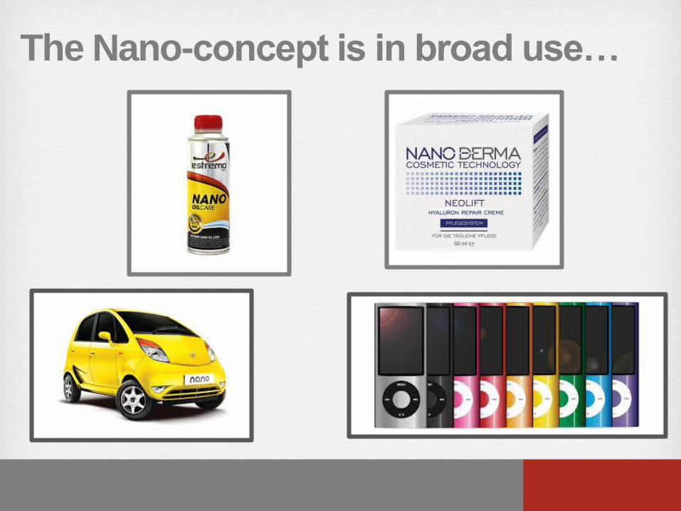
The Nano-concept is in broad use…

… but what is really Nano Science?
Molecule
100,000 smaller
Small isDifferent!
Nano size yields new materials, properties & functions
Human Hair
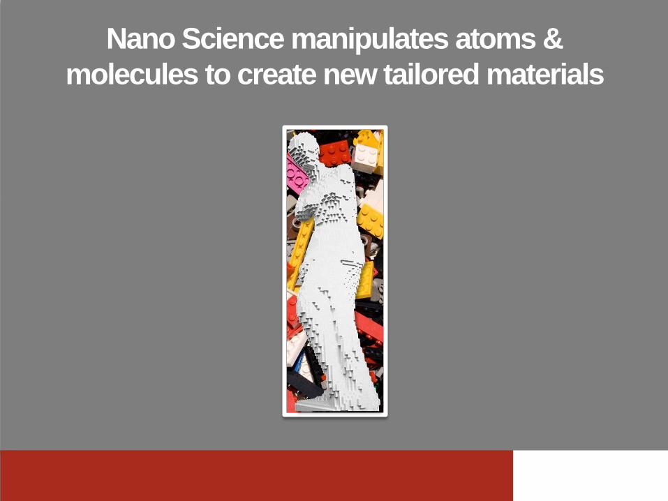
Nano Science manipulates atoms &
molecules to create new tailored materials
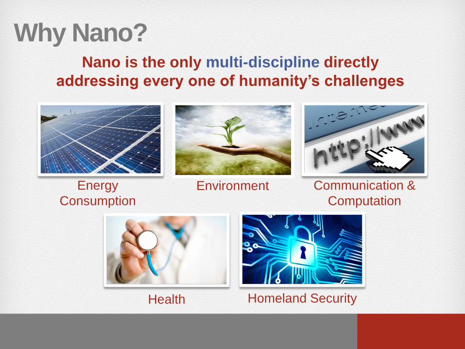
Why Nano?Nano is the only multi-discipline directly
addressing every one of humanity’s challenges
Energy
Consumption
Communication &
Computation
Health Homeland Security
Environment
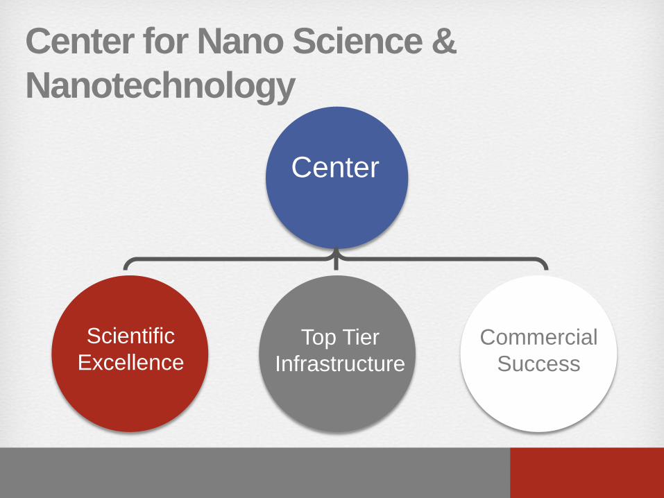
Center for Nano Science &
Nanotechnology
Commercial
Success
Top Tier
Infrastructure
Scientific
Excellence
Center

Excellence in 2007-2014
INAB
2nd Place1st Place
16 grants
ERC
16
Crite
ria
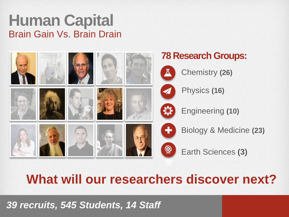
Human CapitalBrain Gain Vs. Brain Drain
What will our researchers discover next?
39 recruits, 545 Students, 14 Staff
78 Research Groups:
Chemistry (26)
+
Earth Sciences (3)
Biology & Medicine (23)
Engineering (10)
Physics (16)
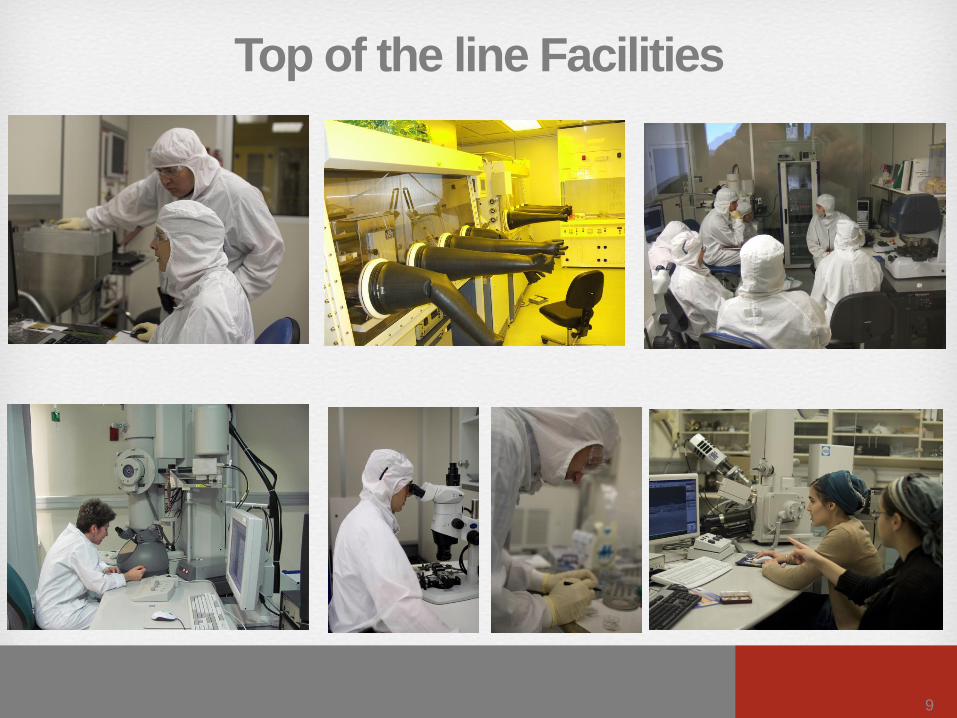
Top of the line Facilities
9
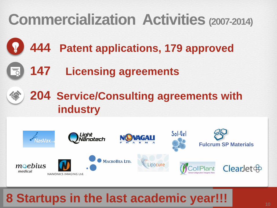
Commercialization Activities (2007-2014)
Fulcrum SP Materials
10
444 Patent applications, 179 approved
147 Licensing agreements
204 Service/Consulting agreements with
industry
8 Startups in the last academic year!!!
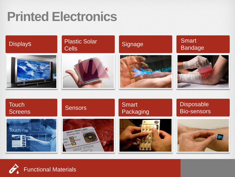
Printed Electronics
Displays Plastic Solar
CellsSignage
Smart
Bandage
Touch
ScreensSensors
Smart
Packaging
Disposable
Bio-sensors
Functional Materials

Functional Nano Coatings
Paints & Coating
Thermo solar
collectors
Greenhouse
Plastic Sheets
Food
Packaging
Composite films for
LED light tuningAnti Bio-fouling films
Functional Materials
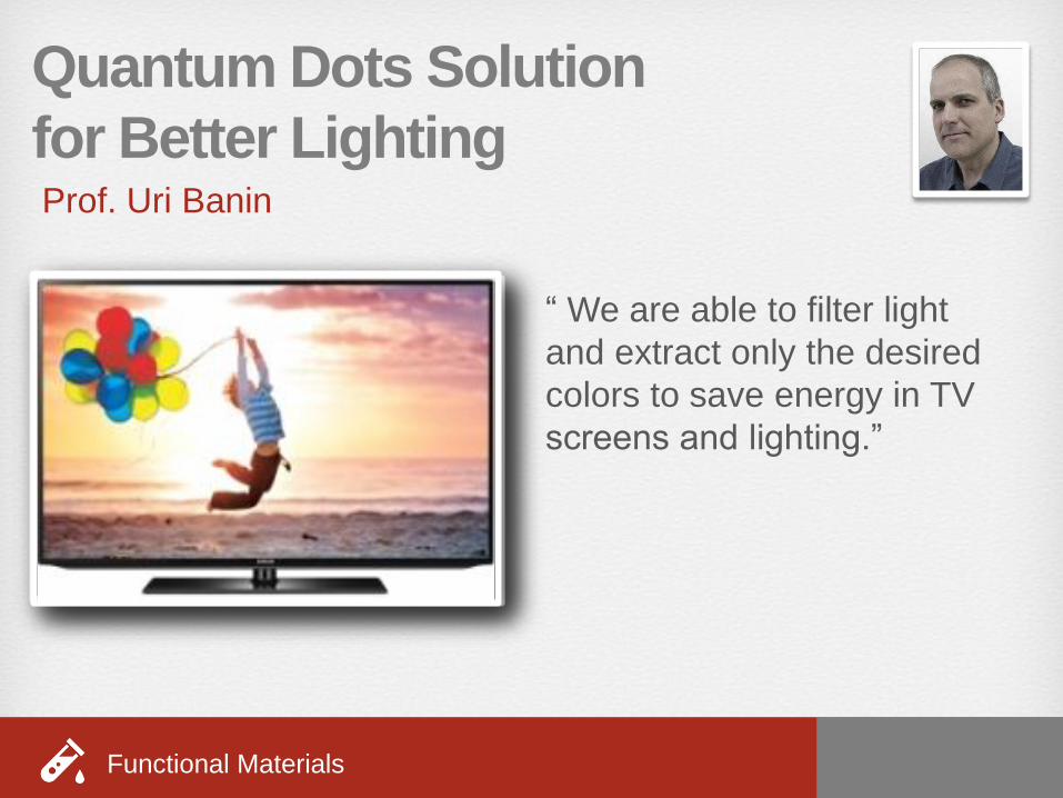
Prof. Uri Banin
Quantum Dots Solution
for Better Lighting
“ We are able to filter light
and extract only the desired
colors to save energy in TV
screens and lighting.”
Functional Materials
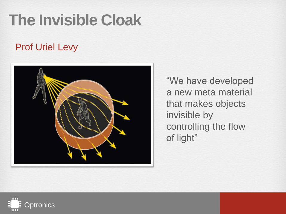
The Invisible Cloak
Prof Uriel Levy
“We have developed
a new meta material
that makes objects
invisible by
controlling the flow
of light”
Optronics

16
Computer speed is increasing

17
Optical communication is everywhere!

The problem of photonics technology
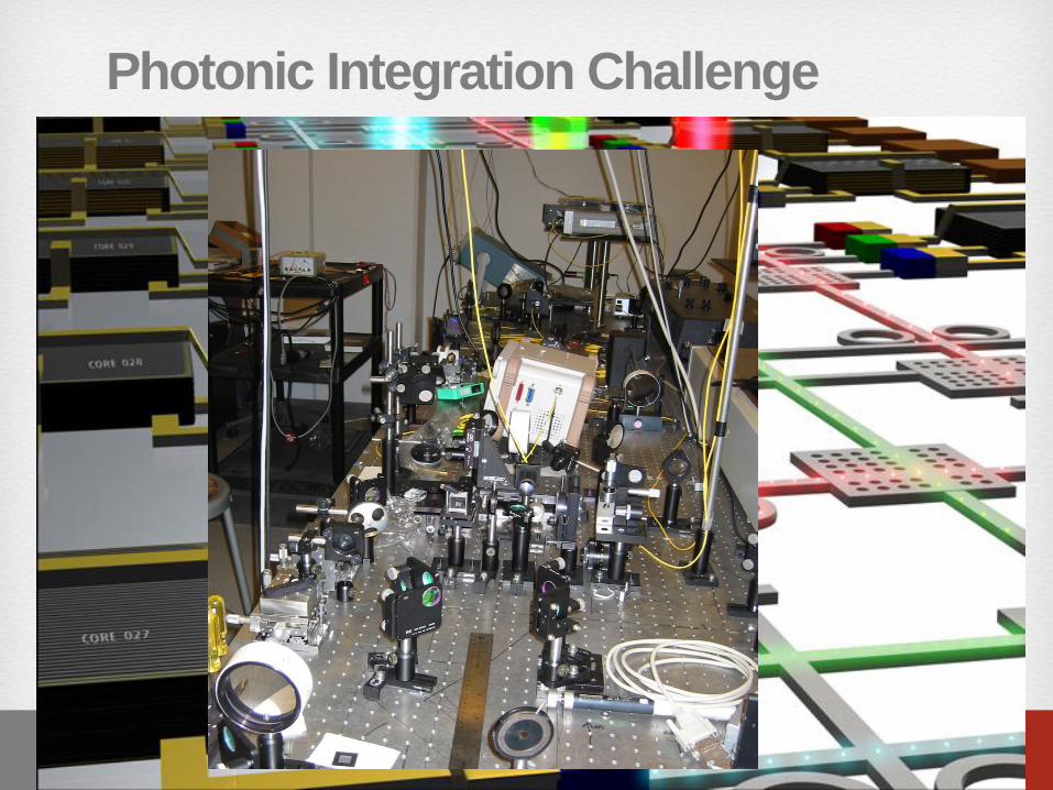
Photonic Integration Challenge
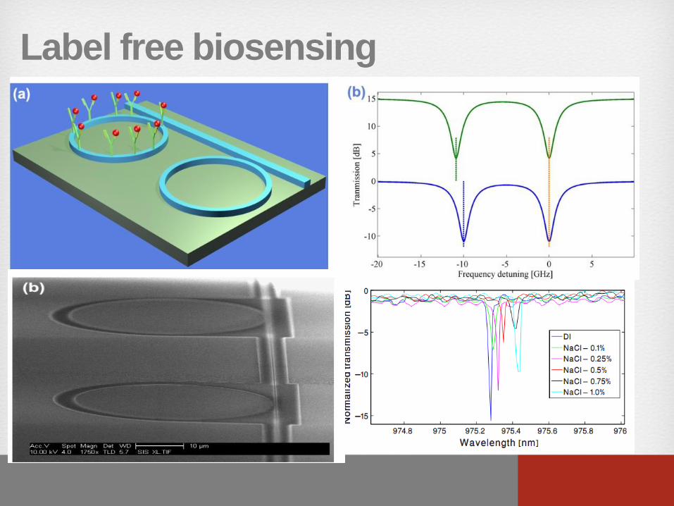
Label free biosensing
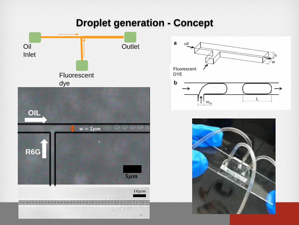
Oil
Inlet
Fluorescent
dye
Outlet
𝒘 = 𝟐𝝁𝒎
Fluorescent
DYE
Droplet generation - Concept
𝒅 = 𝟑𝝁𝒎
OIL
R6G
𝟓𝝁𝒎
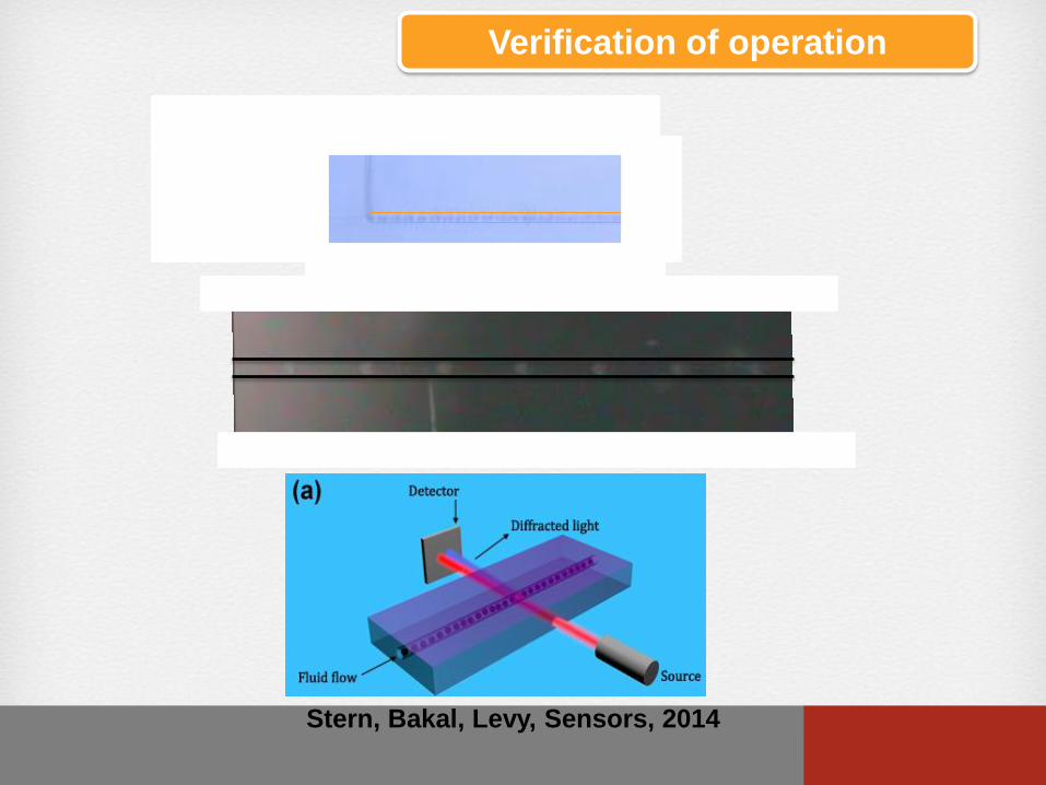
Verification of operation
Stern, Bakal, Levy, Sensors, 2014
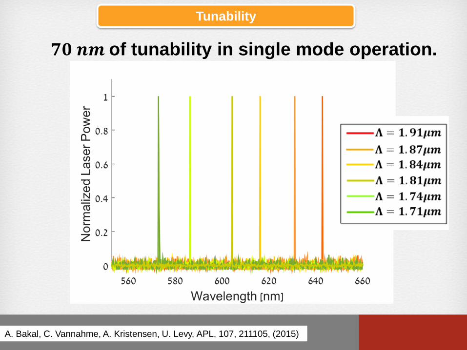
Tunability
𝟕𝟎 𝒏𝒎 of tunability in single mode operation.
A. Bakal, C. Vannahme, A. Kristensen, U. Levy, APL, 107, 211105, (2015)
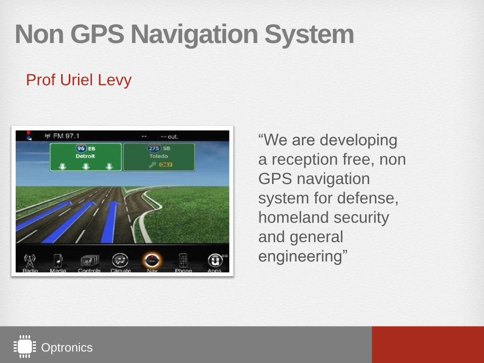
Non GPS Navigation System
Prof Uriel Levy
“We are developing
a reception free, non
GPS navigation
system for defense,
homeland security
and general
engineering”
Optronics
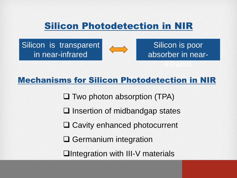
Silicon is transparent
in near-infrared
Silicon is poor
absorber in near-
infrared
Mechanisms for Silicon Photodetection in NIR
Two photon absorption (TPA)
Insertion of midbandgap states
Cavity enhanced photocurrent
Germanium integration
Integration with III-V materials
Silicon Photodetection in NIR

Schottky Barrier Photodetection
Internal photoemission process
PROBLEM
Small interaction volume between photons and electrons in metal
Large electron momentum mismatch between metal and semiconductor
Plasmonics can help!

Fabricated device
500nm20mm
50nm
SU8
Al
Si
SU8
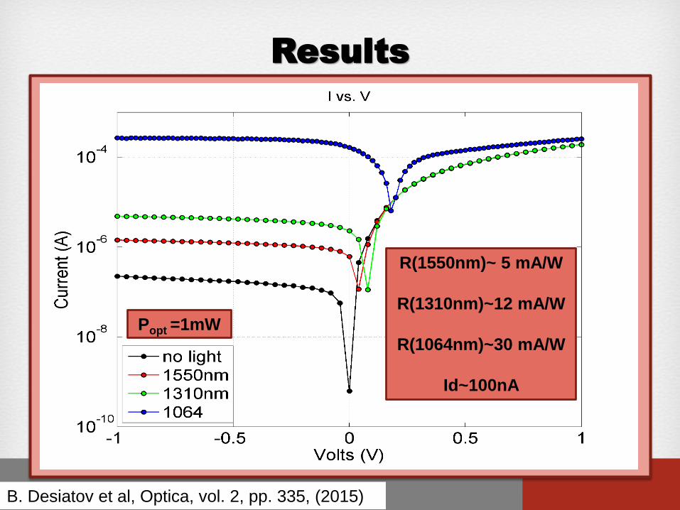
Results
laser
lens
stage
DUT
R(1550nm)~ 5 mA/W
R(1310nm)~12 mA/W
R(1064nm)~30 mA/W
Id~100nA
Popt =1mW
B. Desiatov et al, Optica, vol. 2, pp. 335, (2015)
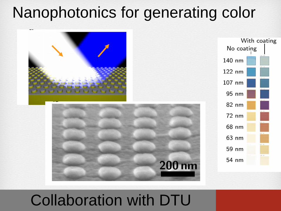
Nanophotonics for generating color
Collaboration with DTU