Embed Size (px)
Citation preview
Science and applications of Tailored Nanostructures 214 214
11
Nanotechnology, Nanomaterials and Thin Films for Energy Applications
L.L. Noto, F.V. Molefe, P.S. Mbule, G. Kabongo, M. Khenfouch, B.M. Mothudi, M.S. Dhlamini
Department of Physics, University of South Africa, P.O. Box 392, Pretoria ZA0003, South Africa.
Outline Introduction…………….…………….…………….…………….…………….…………….…………….…………….……………… 215 Preparation of Nanomaterials and Thin Films.................................................................................. 215 Nanotechnology in Light Emitting Diodes ………………….…….………………………………………………............ 218 Nanotechnology Applied in Solar Cells ………………….…….…………………………….….……………................. 220 Nanotechnology in Persistent Luminescence for Home lighting ………………….…….…………..…........... 227 Graphene Nanomaterials for Energy Conservation………….………………………………………………………….. 231 Acknowledgement ………………….…….….…………………………………………………………………………................ 235 References………………………………………………………………………………………………………………………………….. 235
Science and applications of Tailored Nanostructures 215 215
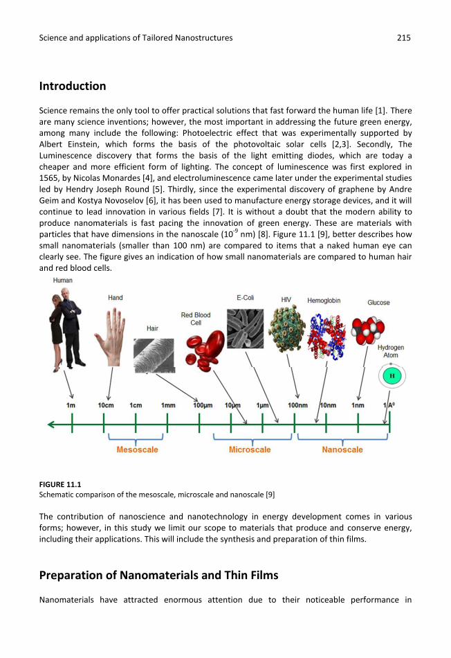
Introduction Science remains the only tool to offer practical solutions that fast forward the human life [1]. There are many science inventions; however, the most important in addressing the future green energy, among many include the following: Photoelectric effect that was experimentally supported by Albert Einstein, which forms the basis of the photovoltaic solar cells [2,3]. Secondly, The Luminescence discovery that forms the basis of the light emitting diodes, which are today a cheaper and more efficient form of lighting. The concept of luminescence was first explored in 1565, by Nicolas Monardes [4], and electroluminescence came later under the experimental studies led by Hendry Joseph Round [5]. Thirdly, since the experimental discovery of graphene by Andre Geim and Kostya Novoselov [6], it has been used to manufacture energy storage devices, and it will continue to lead innovation in various fields [7]. It is without a doubt that the modern ability to produce nanomaterials is fast pacing the innovation of green energy. These are materials with particles that have dimensions in the nanoscale (10
-9 nm) [8]. Figure 11.1 [9], better describes how
small nanomaterials (smaller than 100 nm) are compared to items that a naked human eye can clearly see. The figure gives an indication of how small nanomaterials are compared to human hair and red blood cells.
FIGURE 11.1 Schematic comparison of the mesoscale, microscale and nanoscale [9] The contribution of nanoscience and nanotechnology in energy development comes in various forms; however, in this study we limit our scope to materials that produce and conserve energy, including their applications. This will include the synthesis and preparation of thin films.
Preparation of Nanomaterials and Thin Films
Nanomaterials have attracted enormous attention due to their noticeable performance in
Science and applications of Tailored Nanostructures 216 216
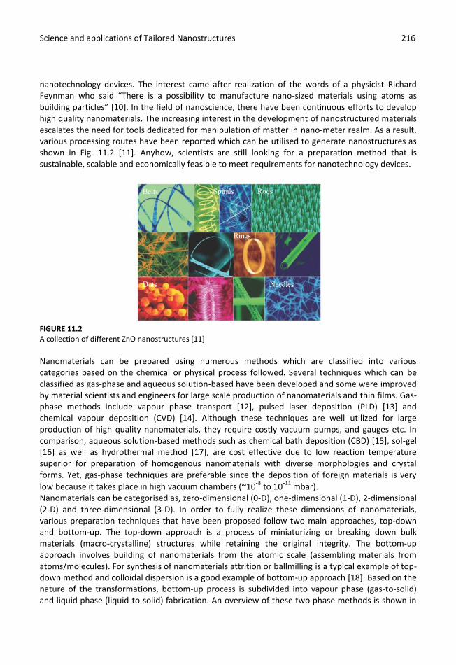
nanotechnology devices. The interest came after realization of the words of a physicist Richard Feynman who said “There is a possibility to manufacture nano-sized materials using atoms as building particles” *10+. In the field of nanoscience, there have been continuous efforts to develop high quality nanomaterials. The increasing interest in the development of nanostructured materials escalates the need for tools dedicated for manipulation of matter in nano-meter realm. As a result, various processing routes have been reported which can be utilised to generate nanostructures as shown in Fig. 11.2 [11]. Anyhow, scientists are still looking for a preparation method that is sustainable, scalable and economically feasible to meet requirements for nanotechnology devices.
FIGURE 11.2 A collection of different ZnO nanostructures [11] Nanomaterials can be prepared using numerous methods which are classified into various categories based on the chemical or physical process followed. Several techniques which can be classified as gas-phase and aqueous solution-based have been developed and some were improved by material scientists and engineers for large scale production of nanomaterials and thin films. Gas-phase methods include vapour phase transport [12], pulsed laser deposition (PLD) [13] and chemical vapour deposition (CVD) [14]. Although these techniques are well utilized for large production of high quality nanomaterials, they require costly vacuum pumps, and gauges etc. In comparison, aqueous solution-based methods such as chemical bath deposition (CBD) [15], sol-gel [16] as well as hydrothermal method [17], are cost effective due to low reaction temperature superior for preparation of homogenous nanomaterials with diverse morphologies and crystal forms. Yet, gas-phase techniques are preferable since the deposition of foreign materials is very
low because it takes place in high vacuum chambers (~10-8 to 10-
11 mbar).
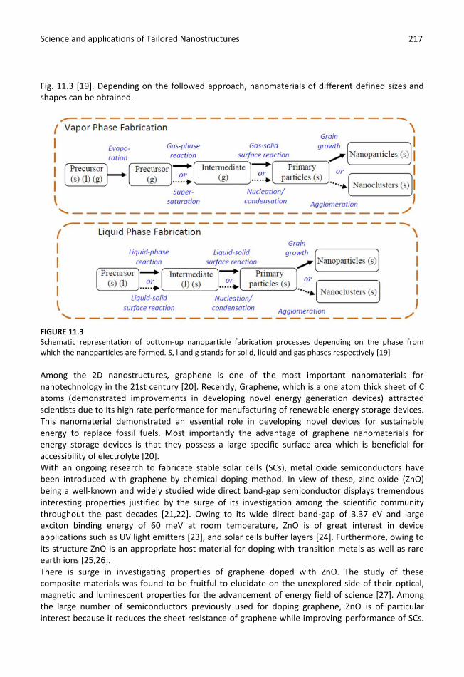
Nanomaterials can be categorised as, zero-dimensional (0-D), one-dimensional (1-D), 2-dimensional (2-D) and three-dimensional (3-D). In order to fully realize these dimensions of nanomaterials, various preparation techniques that have been proposed follow two main approaches, top-down and bottom-up. The top-down approach is a process of miniaturizing or breaking down bulk materials (macro-crystalline) structures while retaining the original integrity. The bottom-up approach involves building of nanomaterials from the atomic scale (assembling materials from atoms/molecules). For synthesis of nanomaterials attrition or ballmilling is a typical example of top-down method and colloidal dispersion is a good example of bottom-up approach [18]. Based on the nature of the transformations, bottom-up process is subdivided into vapour phase (gas-to-solid) and liquid phase (liquid-to-solid) fabrication. An overview of these two phase methods is shown in
Science and applications of Tailored Nanostructures 217 217
Fig. 11.3 [19]. Depending on the followed approach, nanomaterials of different defined sizes and shapes can be obtained.
FIGURE 11.3 Schematic representation of bottom-up nanoparticle fabrication processes depending on the phase from which the nanoparticles are formed. S, l and g stands for solid, liquid and gas phases respectively [19]
Among the 2D nanostructures, graphene is one of the most important nanomaterials for nanotechnology in the 21st century [20]. Recently, Graphene, which is a one atom thick sheet of C atoms (demonstrated improvements in developing novel energy generation devices) attracted scientists due to its high rate performance for manufacturing of renewable energy storage devices. This nanomaterial demonstrated an essential role in developing novel devices for sustainable energy to replace fossil fuels. Most importantly the advantage of graphene nanomaterials for energy storage devices is that they possess a large specific surface area which is beneficial for accessibility of electrolyte [20]. With an ongoing research to fabricate stable solar cells (SCs), metal oxide semiconductors have been introduced with graphene by chemical doping method. In view of these, zinc oxide (ZnO) being a well-known and widely studied wide direct band-gap semiconductor displays tremendous interesting properties justified by the surge of its investigation among the scientific community throughout the past decades [21,22]. Owing to its wide direct band-gap of 3.37 eV and large exciton binding energy of 60 meV at room temperature, ZnO is of great interest in device applications such as UV light emitters [23], and solar cells buffer layers [24]. Furthermore, owing to its structure ZnO is an appropriate host material for doping with transition metals as well as rare earth ions [25,26]. There is surge in investigating properties of graphene doped with ZnO. The study of these composite materials was found to be fruitful to elucidate on the unexplored side of their optical, magnetic and luminescent properties for the advancement of energy field of science [27]. Among the large number of semiconductors previously used for doping graphene, ZnO is of particular interest because it reduces the sheet resistance of graphene while improving performance of SCs.
Science and applications of Tailored Nanostructures 218 218
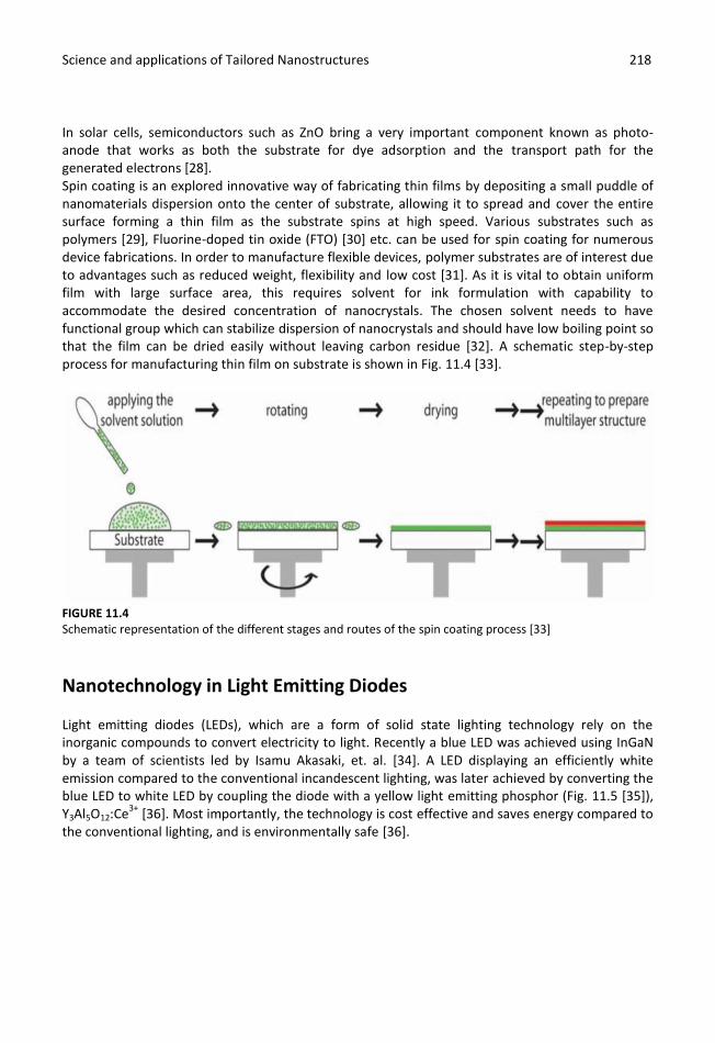
In solar cells, semiconductors such as ZnO bring a very important component known as photo-anode that works as both the substrate for dye adsorption and the transport path for the generated electrons [28]. Spin coating is an explored innovative way of fabricating thin films by depositing a small puddle of nanomaterials dispersion onto the center of substrate, allowing it to spread and cover the entire surface forming a thin film as the substrate spins at high speed. Various substrates such as polymers [29], Fluorine-doped tin oxide (FTO) [30] etc. can be used for spin coating for numerous device fabrications. In order to manufacture flexible devices, polymer substrates are of interest due to advantages such as reduced weight, flexibility and low cost [31]. As it is vital to obtain uniform film with large surface area, this requires solvent for ink formulation with capability to accommodate the desired concentration of nanocrystals. The chosen solvent needs to have functional group which can stabilize dispersion of nanocrystals and should have low boiling point so that the film can be dried easily without leaving carbon residue [32]. A schematic step-by-step process for manufacturing thin film on substrate is shown in Fig. 11.4 [33].
FIGURE 11.4 Schematic representation of the different stages and routes of the spin coating process [33]
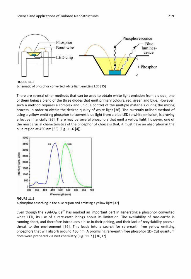
Nanotechnology in Light Emitting Diodes Light emitting diodes (LEDs), which are a form of solid state lighting technology rely on the inorganic compounds to convert electricity to light. Recently a blue LED was achieved using InGaN by a team of scientists led by Isamu Akasaki, et. al. [34]. A LED displaying an efficiently white emission compared to the conventional incandescent lighting, was later achieved by converting the blue LED to white LED by coupling the diode with a yellow light emitting phosphor (Fig. 11.5 [35]), Y3Al5O12:Ce
3+ [36]. Most importantly, the technology is cost effective and saves energy compared to
the conventional lighting, and is environmentally safe [36].
Science and applications of Tailored Nanostructures 219 219
FIGURE 11.5 Schematic of phosphor converted white light emitting LED [35] There are several other methods that can be used to obtain white light emission from a diode, one of them being a blend of the three diodes that emit primary colours: red, green and blue. However, such a method requires a complex and unique control of the multiple materials during the mixing process, in order to obtain the desired quality of white light [36]. The currently utilised method of using a yellow emitting phosphor to convert blue light from a blue LED to white emission, is proving effective financially [36]. There may be several phosphors that emit a yellow light; however, one of the most crucial characteristics of the phosphor of choice is that, it must have an absorption in the blue region at 450 nm [36] (Fig. 11.6 [4]).
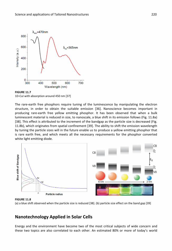
FIGURE 11.6 A phosphor absorbing in the blue region and emitting a yellow light [37] Even though the Y3Al5O12:Ce
3+ has marked an important part in generating a phosphor converted
white LED, its use of a rare-earth brings about its limitation. The availability of rare-earths is running short, and therefore introduces a hike in their pricing, and their lack of recyclability poses a threat to the environment [36]. This leads into a search for rare-earth free yellow emitting phosphors that will absorb around 450 nm. A promising rare-earth free phosphor 1D- CuI quantum dots were prepared via wet chemistry (Fig. 11.7 ) [36,37].
Science and applications of Tailored Nanostructures 220 220
FIGURE 11.7 1D-CuI with absorption around 450 nm [37]
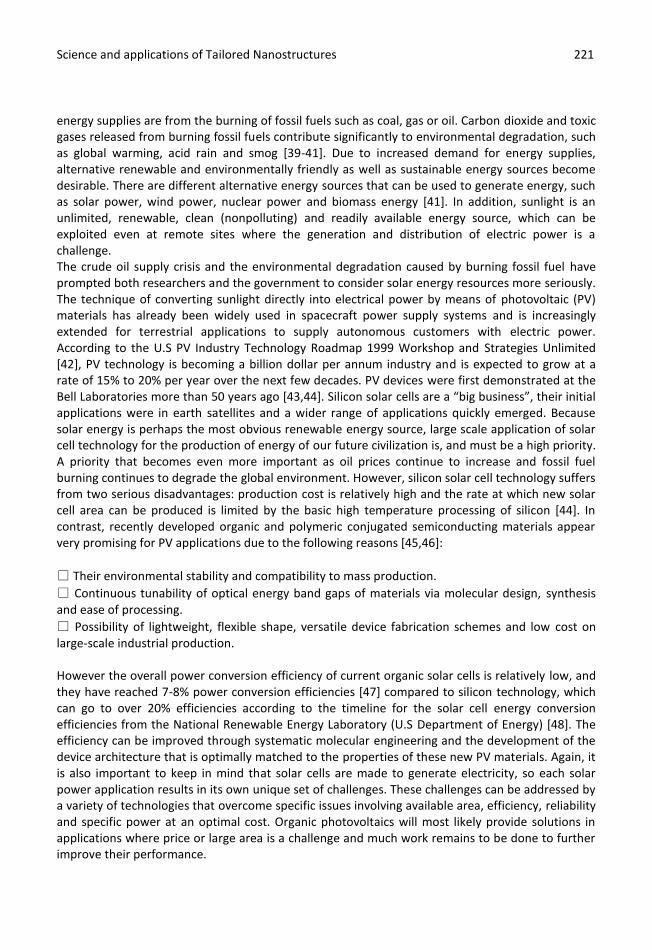
The rare-earth free phosphors require tuning of the luminescence by manipulating the electron structure, in order to obtain the suitable emission [36]. Nanoscience becomes important in producing rare-earth free yellow emitting phosphor. It has been observed that when a bulk luminescent material is reduced in size, to nanoscale, a blue shift in its emission follows (Fig. 11.8a) [38]. This effect is attributed to the increment of the bandgap as the particle size is decreased (Fig. 11.8b), which originates from spatial confinement [39]. The ability to shift the emission wavelength by tuning the particle sizes will in the future enable us to produce a yellow emitting phosphor that is rare earth free, and which meets all the necessary requirements for the phosphor converted white light emitting diode.
FIGURE 11.8 (a) a blue shift observed when the particle size is reduced [38]. (b) particle size effect on the band gap [39]
Nanotechnology Applied in Solar Cells
Energy and the environment have become two of the most critical subjects of wide concern and these two topics are also correlated to each other. An estimated 80% or more of today’s world
Science and applications of Tailored Nanostructures 221 221
energy supplies are from the burning of fossil fuels such as coal, gas or oil. Carbon dioxide and toxic gases released from burning fossil fuels contribute significantly to environmental degradation, such as global warming, acid rain and smog [39-41]. Due to increased demand for energy supplies, alternative renewable and environmentally friendly as well as sustainable energy sources become desirable. There are different alternative energy sources that can be used to generate energy, such as solar power, wind power, nuclear power and biomass energy [41]. In addition, sunlight is an unlimited, renewable, clean (nonpolluting) and readily available energy source, which can be exploited even at remote sites where the generation and distribution of electric power is a challenge. The crude oil supply crisis and the environmental degradation caused by burning fossil fuel have prompted both researchers and the government to consider solar energy resources more seriously. The technique of converting sunlight directly into electrical power by means of photovoltaic (PV) materials has already been widely used in spacecraft power supply systems and is increasingly extended for terrestrial applications to supply autonomous customers with electric power. According to the U.S PV Industry Technology Roadmap 1999 Workshop and Strategies Unlimited [42], PV technology is becoming a billion dollar per annum industry and is expected to grow at a rate of 15% to 20% per year over the next few decades. PV devices were first demonstrated at the Bell Laboratories more than 50 years ago [43,44]. Silicon solar cells are a “big business”, their initial applications were in earth satellites and a wider range of applications quickly emerged. Because solar energy is perhaps the most obvious renewable energy source, large scale application of solar cell technology for the production of energy of our future civilization is, and must be a high priority. A priority that becomes even more important as oil prices continue to increase and fossil fuel burning continues to degrade the global environment. However, silicon solar cell technology suffers from two serious disadvantages: production cost is relatively high and the rate at which new solar cell area can be produced is limited by the basic high temperature processing of silicon [44]. In contrast, recently developed organic and polymeric conjugated semiconducting materials appear very promising for PV applications due to the following reasons [45,46]:
Their environmental stability and compatibility to mass production.
Continuous tunability of optical energy band gaps of materials via molecular design, synthesis and ease of processing.
Possibility of lightweight, flexible shape, versatile device fabrication schemes and low cost on large-scale industrial production. However the overall power conversion efficiency of current organic solar cells is relatively low, and they have reached 7-8% power conversion efficiencies [47] compared to silicon technology, which can go to over 20% efficiencies according to the timeline for the solar cell energy conversion efficiencies from the National Renewable Energy Laboratory (U.S Department of Energy) [48]. The efficiency can be improved through systematic molecular engineering and the development of the device architecture that is optimally matched to the properties of these new PV materials. Again, it is also important to keep in mind that solar cells are made to generate electricity, so each solar power application results in its own unique set of challenges. These challenges can be addressed by a variety of technologies that overcome specific issues involving available area, efficiency, reliability and specific power at an optimal cost. Organic photovoltaics will most likely provide solutions in applications where price or large area is a challenge and much work remains to be done to further improve their performance.
Science and applications of Tailored Nanostructures 222 222
In order to improve the performance, stability, and lifetime of bulk-heterojunction organic solar cells (BHJ-OSCs), researchers are faced with many challenges that need to be addressed. Appropriate design and fabrication of BHJ-OSCs are of great importance for their development. Therefore the major challenge lies in fabricating BHJ-OSCs in which free-charge-carrier generation is a critical step [49]. Despite high attainable external quantum efficiencies, overall power conversion efficiencies of BHJ-OSCs reported are still low due to inferior charge transport properties and the limited solar spectral absorption range of the polymer active layer. On the other hand, endeavors in synthesis and development of novel low band-gap polymers are being carried out to harvest the major part of the solar spectrum [49-51]. Fabrication parameters such as solvent selection and annealing treatment are also critical factors in film morphology of the active layer in BHJ-OSCs. The overall effects of morphology manipulation assist in forming an interpenetrating network of donor and acceptor molecules, facilitating both charge transfer and transport. For efficient BHJ OSCs, transparent and conductive interfacial materials/buffer layers which are inserted between an active layer and top metal electrode are required. The role of this buffer layer is not only to form an electron selective layer but also to form an electrical contact to the metal electrode. Recently, a thin layer (10-20 nm) of solution processed titanium dioxide (TiO2) or zinc oxide (ZnO) has been successfully applied as an interfacial layer in the normal and inverted geometry of BHJ-OSCs. Furthermore, BHJ-OSCs can suffer from degradation of the top electrode, which is normally a low work-function metal such as aluminum (Al) that is reactive and can easily be oxidized in air. Alternatively, inverted device geometry is an attractive concept to improve their longevity because a metal electrode such as silver (Ag) or gold (Au), with higher work-function is used. Moreover, this geometry brings the possibility of significantly improving the stability of the BHJ-OSCs in air [52-54]. Conventional and inverted bulk-heterojunction organic solar cells (BHJ-OSCs) are of great interest due to their potential applications as sources of renewable energy and for being able to reach power conversion efficiencies (PCE) of 3-9 % [55,56]. Among all possible materials that have been used as photo-active layers, the most widely used material system in BHJOSCs is the blend of poly (3-hexylthiophene-2,5-diyl) polymer or P3HT and (6,6) phenyl butyric acid methyl ester fullerene or PCBM. The layer is commonly referred to as P3HT:PCBM. Investigations show that OSCs made from this blend have power conversion efficiencies that can go up to 3-5 % and this indicate the reasonable capacity of the P3HT:PCBM blend to attain high efficiencies in future [57]. Significant advances in PCE of BHJ-OSCs are achieved by the improvement of the photo-active layer morphology, optimization of interfacial area of the layers in the device, charge mobility and engineering of the device architecture. In addition, conventional geometry of BHJ-OSCs can suffer from degradation of the top Al electrode which is reactive in air and oxidizes easily [58]. Therefore, the inclusion of the ZnO layer is essential and it is attributed to a few different reasons. It prevents the quenching of photo-generated excitons in the active layer by the Al cathode. It also prevents the diffusion of Al atoms in the active layer upon deposition and post-deposition annealing, as this may cause the recombination sites for excitons within the active layer. In addition the ZnO layer does not only act as the buffer layer, it forms the electrical contact with the Al cathode to help overcome or reduce the serial resistance in the device. On the other hand, inverted geometry is said to improve the longevity and air stability of BHJ-OSCs because it uses electrode (Ag) and interface materials with a higher work function [42]. Again, typical electron conductors such as ZnO and TiO2 nanoparticles serve as intermediate and/or protective layers between an electrode and organic photo-active layer and therefore helps improve the performance of OSCs [59,60].
Science and applications of Tailored Nanostructures 223 223
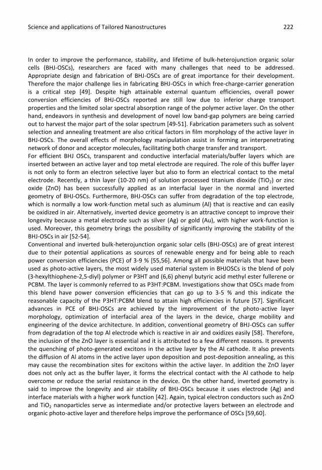
Device Fabrication A glass substrate pre-coated with ITO is cleaned ultrasonically using isopropanol and acetone consecutively. The substrates is then dried at ~ 80
oC in an oven and treated in an ultraviolet ozone
generator. A thin layer of poly(3,4-ethylenedioxythiophene):polystyrenesulfonic acid (PEDOT:PSS) (CLEVIOS™ AI 4083) spin coated (see Fig. 11.9) on a substrate at the speed of 4000 rpm for 35 seconds then followed by drying in an oven. The photo active P3HT:PCBM blend layer (P3HT, Aldrich/ PCBM, Nano-C), with weight ratio of 1:0.6, dissolved from a blend solution of chlorobenzene solvent and electron extracting layer of ZnO nanoparticles is spin coated at the speed of 4000 rpm for 35 seconds and this is followed by the deposition of the Al layer (~ 100 nm) thermally evaporated at ~ 1x10
-6 Torr pressure through a shadow mask defining the device area of
0.12 cm2. The conventional device have a glass/ITO/PEDOT:PSS/P3HT:PCBM/ZnO/Al configuration
and under identical processing conditions, the inverted device also have a glass/ITO/ZnO/P3HT:PCBM/PEDOT: PSS/Ag configuration.
FIGURE 11.9 diagram of spin coating process and vacuum evaporator [61,62]
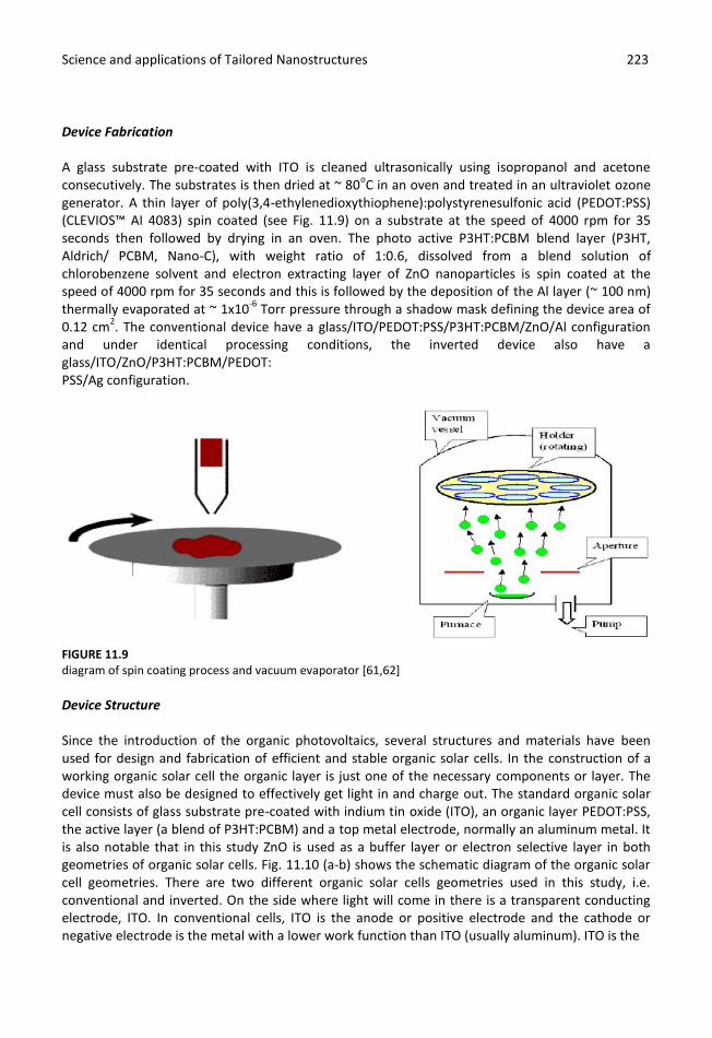
Device Structure Since the introduction of the organic photovoltaics, several structures and materials have been used for design and fabrication of efficient and stable organic solar cells. In the construction of a working organic solar cell the organic layer is just one of the necessary components or layer. The device must also be designed to effectively get light in and charge out. The standard organic solar cell consists of glass substrate pre-coated with indium tin oxide (ITO), an organic layer PEDOT:PSS, the active layer (a blend of P3HT:PCBM) and a top metal electrode, normally an aluminum metal. It is also notable that in this study ZnO is used as a buffer layer or electron selective layer in both geometries of organic solar cells. Fig. 11.10 (a-b) shows the schematic diagram of the organic solar cell geometries. There are two different organic solar cells geometries used in this study, i.e. conventional and inverted. On the side where light will come in there is a transparent conducting electrode, ITO. In conventional cells, ITO is the anode or positive electrode and the cathode or negative electrode is the metal with a lower work function than ITO (usually aluminum). ITO is the
Science and applications of Tailored Nanostructures 224 224
cathode in inverted cells and a metal with a work function greater than ITO (usually silver or gold) is the anode. However, there are advantages and drawbacks for each geometry. Conventional geometry results in relatively high efficiencies, while inverted cells are both more stable and more amenable to solution processing. There is also often a glass substrate that provides mechanical support and anti-reflection coatings to help to minimize losses due to nonabsorption. Care must be taken with the attachment of the electrodes to the organic materials, because the process may form an insulating layer. However, strategies have been developed for certain materials, such as adding buffer layers to solve the problem of instability and degradation [63]. The energy level alignment in the organic solar cells is schematically shown in Fig. 11.10 (c-d) (Energies are referenced to the vacuum level).. (Energies are referenced to the vacuum level). While P3HT and PCBM form a donoracceptor heterojunction that facilitates the dissociation of photo-generated excitons (bound electron-hole pairs), the lower conduction band edge of ZnO as compared to the lowest unoccupied molecular orbital (LUMO) of P3HT may also lead to dissociation of excitons in P3HT via rapid electron transfer to ZnO. The similar electron affinities of ZnO and PCBM also suggest that there is a negligible barrier height for electron transport from PCBM towards the Al cathode. Furthermore, the very deep valence band of ZnO creates a large barrier height to block hole injection from the P3HT: PCBM active layer into ZnO [64].
FIGURE 11.10 (a) Conventional device structure, (b) Inverted structure and their Energy level diagrams (c and d). The energies are referenced to the vacuum level [30]
Science and applications of Tailored Nanostructures 225 225
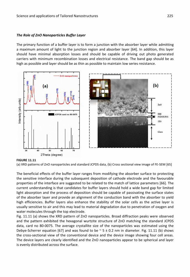
The Role of ZnO Nanoparticles Buffer Layer The primary function of a buffer layer is to form a junction with the absorber layer while admitting a maximum amount of light to the junction region and absorber layer [64]. In addition, this layer should have minimal absorption losses and should be capable of driving out photo generated carriers with minimum recombination losses and electrical resistance. The band gap should be as high as possible and layer should be as thin as possible to maintain low series resistance.
FIGURE 11.11 (a) XRD patterns of ZnO nanoparticles and standard JCPDS data, (b) Cross sectional view image of FE-SEM [65]
The beneficial effects of the buffer layer ranges from modifying the absorber surface to protecting the sensitive interface during the subsequent deposition of cathode electrode and the favourable properties of the interface are suggested to be related to the match of lattice parameters [66]. The current understanding is that candidates for buffer layers should hold a wide band gap for limited light absorption and the process of deposition should be capable of passivating the surface states of the absorber layer and provide an alignment of the conduction band with the absorber to yield high efficiencies. Buffer layers also enhance the stability of the solar cells as the active layer is usually sensitive to air and this may lead to material degradation due to penetration of oxygen and water molecules through the top electrode. Fig. 11.11 (a) shows the XRD pattern of ZnO nanoparticles. Broad diffraction peaks were observed and the pattern exhibited the hexagonal wurtzite structure of ZnO matching the standard JCPDS data, card no 80-0075. The average crystallite size of the nanoparticles was estimated using the Debye-Scherrer equation [67] and was found to be ~ 5 ± 0.2 nm in diameter. Fig. 11.11 (b) shows the cross-sectional view of the conventional device and the device image showing four cell areas. The device layers are clearly identified and the ZnO nanoparticles appear to be spherical and layer is evenly distributed across the surface.
Science and applications of Tailored Nanostructures 226 226
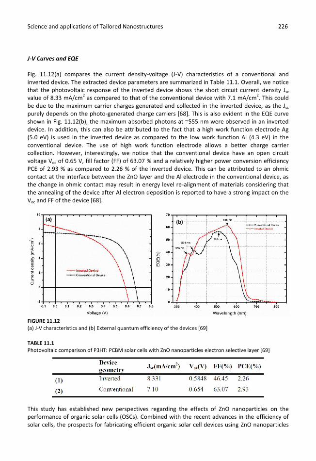
J-V Curves and EQE Fig. 11.12(a) compares the current density-voltage (J-V) characteristics of a conventional and inverted device. The extracted device parameters are summarized in Table 11.1. Overall, we notice that the photovoltaic response of the inverted device shows the short circuit current density Jsc value of 8.33 mA/cm
2 as compared to that of the conventional device with 7.1 mA/cm
2. This could
be due to the maximum carrier charges generated and collected in the inverted device, as the Jsc purely depends on the photo-generated charge carriers [68]. This is also evident in the EQE curve shown in Fig. 11.12(b), the maximum absorbed photons at ~555 nm were observed in an inverted device. In addition, this can also be attributed to the fact that a high work function electrode Ag (5.0 eV) is used in the inverted device as compared to the low work function Al (4.3 eV) in the conventional device. The use of high work function electrode allows a better charge carrier collection. However, interestingly, we notice that the conventional device have an open circuit voltage Voc of 0.65 V, fill factor (FF) of 63.07 % and a relatively higher power conversion efficiency PCE of 2.93 % as compared to 2.26 % of the inverted device. This can be attributed to an ohmic contact at the interface between the ZnO layer and the Al electrode in the conventional device, as the change in ohmic contact may result in energy level re-alignment of materials considering that the annealing of the device after Al electron deposition is reported to have a strong impact on the Voc and FF of the device [68].
FIGURE 11.12 (a) J-V characteristics and (b) External quantum efficiency of the devices [69]
TABLE 11.1 Photovoltaic comparison of P3HT: PCBM solar cells with ZnO nanoparticles electron selective layer [69]
This study has established new perspectives regarding the effects of ZnO nanoparticles on the performance of organic solar cells (OSCs). Combined with the recent advances in the efficiency of solar cells, the prospects for fabricating efficient organic solar cell devices using ZnO nanoparticles
Science and applications of Tailored Nanostructures 227 227
as electron extracting layers are excellent. However, it should be noted that the reproducibility issue of OSCs has not yet been clearly addressed because of several reasons. Firstly, establishing highly reproducible performance of OSCs requires tremendous trial and errors, and poorly reproducible performance is believed to be an intrinsic drawback of organic electronics devices. Secondly, in the device fabrication, there are several process variables: blend solution preparation method, blend ratio, blend layer thickness, PEDOT:PSS thickness, various kinds of PEDOT:PSS with different conductivity, spin casting conditions, cathode structure, annealing conditions and method, oxygen and moisture exposure, encapsulation, illumination set-up and characterization set-up. As a result, it is quite difficult to consistently reproduce the same or relative photovoltaic output from one device to the other. Therefore, many researchers experience significant performance variation even though the devices were fabricated using a consistent procedure. Finally, the results reported in this research indicated that more fundamental questions concerning the influence of ZnO nanoparticles on the performance of organic solar cells must be addressed before rational improvement can be expected. The future work that can be done to continue the research of P3HT:PCBM based solar cells is to look into approaches of light harvesting by choosing low band gap photo-active materials and band gap tuning of conjugated polymers to maximize the efficiency of OSCs. Moreover, ZnO has a lot of defects that might cause instability in the devices. Treatment of ZnO in the UV-Ozone may get rid of some of these defects and significantly change the conductivity thereby enhancing the absorption efficiencies or the overall performance of OSCs.
Nanotechnology in Persistent Luminescence for Home lighting
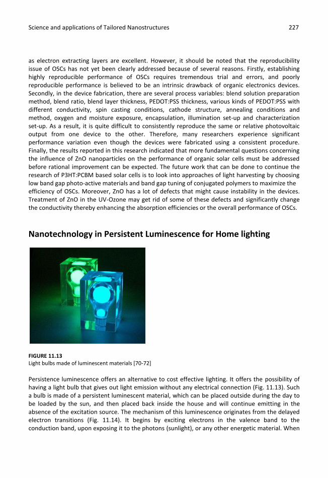
FIGURE 11.13 Light bulbs made of luminescent materials [70-72]
Persistence luminescence offers an alternative to cost effective lighting. It offers the possibility of having a light bulb that gives out light emission without any electrical connection (Fig. 11.13). Such a bulb is made of a persistent luminescent material, which can be placed outside during the day to be loaded by the sun, and then placed back inside the house and will continue emitting in the absence of the excitation source. The mechanism of this luminescence originates from the delayed electron transitions (Fig. 11.14). It begins by exciting electrons in the valence band to the conduction band, upon exposing it to the photons (sunlight), or any other energetic material. When
Science and applications of Tailored Nanostructures 228 228
the excited electrons de-excite to the electron trapping centers with different energies, those trapped in deeper traps are withheld. Those in shallower traps such that room temperature can stimulate them back to the conduction band, will gradually be detrapped in time and will eventually de-excite to luminescent center. The gradual detrapping may last upto several minutes or hours, resulting in a phosphor displaying a long lasting emission, called persistent luminescence [70]. Nanomaterials have a greater surface area compared to bulk materials, and therefore a greater quantity of surface defects. This will generate more surface defects to prolong the persistent luminescence [70].
FIGURE 11.14 Persistent luminescence mechanism [71]
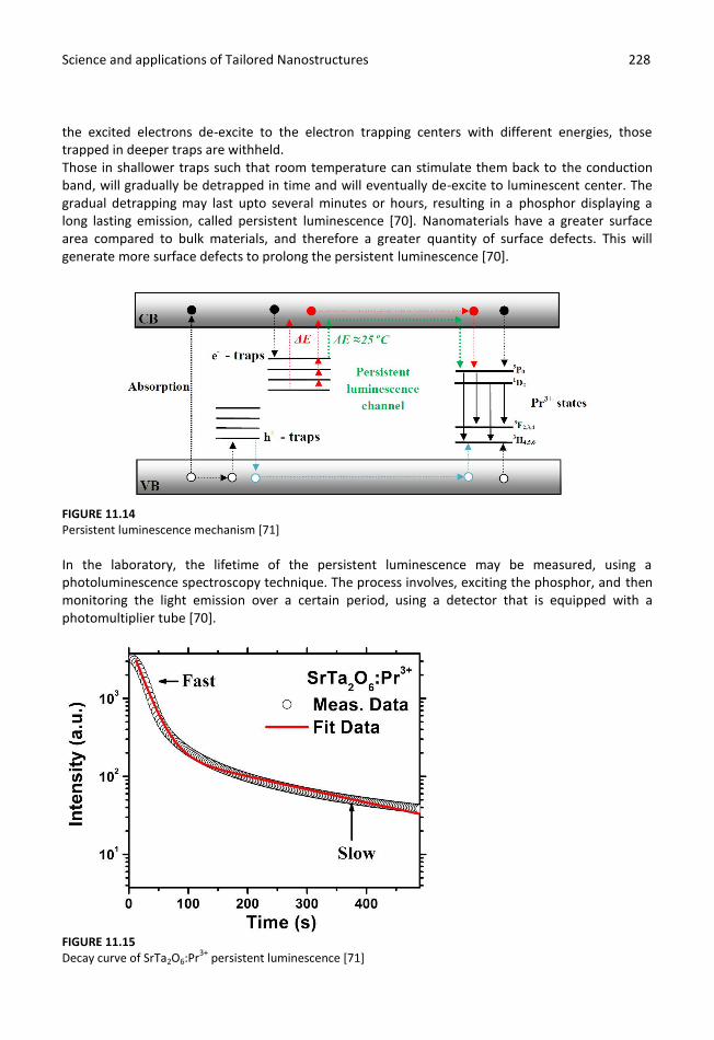
In the laboratory, the lifetime of the persistent luminescence may be measured, using a photoluminescence spectroscopy technique. The process involves, exciting the phosphor, and then monitoring the light emission over a certain period, using a detector that is equipped with a photomultiplier tube [70].
FIGURE 11.15 Decay curve of SrTa2O6:Pr
3+ persistent luminescence [71]
Science and applications of Tailored Nanostructures 229 229
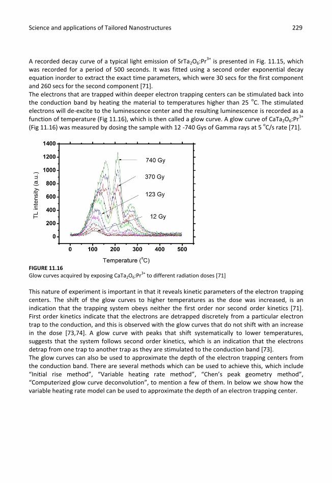
A recorded decay curve of a typical light emission of SrTa2O6:Pr3+
is presented in Fig. 11.15, which was recorded for a period of 500 seconds. It was fitted using a second order exponential decay equation inorder to extract the exact time parameters, which were 30 secs for the first component and 260 secs for the second component [71]. The electrons that are trapped within deeper electron trapping centers can be stimulated back into the conduction band by heating the material to temperatures higher than 25
oC. The stimulated
electrons will de-excite to the luminescence center and the resulting luminescence is recorded as a function of temperature (Fig 11.16), which is then called a glow curve. A glow curve of CaTa2O6:Pr
3+
(Fig 11.16) was measured by dosing the sample with 12 -740 Gys of Gamma rays at 5 oC/s rate [71].
FIGURE 11.16 Glow curves acquired by exposing CaTa2O6:Pr
3+ to different radiation doses [71]
This nature of experiment is important in that it reveals kinetic parameters of the electron trapping centers. The shift of the glow curves to higher temperatures as the dose was increased, is an indication that the trapping system obeys neither the first order nor second order kinetics [71]. First order kinetics indicate that the electrons are detrapped discretely from a particular electron trap to the conduction, and this is observed with the glow curves that do not shift with an increase in the dose [73,74]. A glow curve with peaks that shift systematically to lower temperatures, suggests that the system follows second order kinetics, which is an indication that the electrons detrap from one trap to another trap as they are stimulated to the conduction band [73]. The glow curves can also be used to approximate the depth of the electron trapping centers from the conduction band. There are several methods which can be used to achieve this, which include “Initial rise method”, “Variable heating rate method”, “Chen’s peak geometry method”, “Computerized glow curve deconvolution”, to mention a few of them. In below we show how the variable heating rate model can be used to approximate the depth of an electron trapping center.
Science and applications of Tailored Nanostructures 230 230
FIGURE 11.17 CaTa2O6:Pr
3+ glow curves acquired using varied heating rates [71]
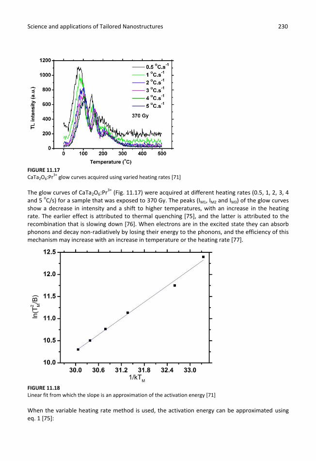
The glow curves of CaTa2O6:Pr
3+ (Fig. 11.17) were acquired at different heating rates (0.5, 1, 2, 3, 4
and 5 oC/s) for a sample that was exposed to 370 Gy. The peaks (IM1, IM2 and IM3) of the glow curves
show a decrease in intensity and a shift to higher temperatures, with an increase in the heating rate. The earlier effect is attributed to thermal quenching [75], and the latter is attributed to the recombination that is slowing down [76]. When electrons are in the excited state they can absorb phonons and decay non-radiatively by losing their energy to the phonons, and the efficiency of this mechanism may increase with an increase in temperature or the heating rate [77].
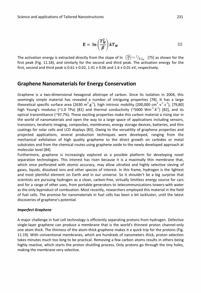
FIGURE 11.18 Linear fit from which the slope is an approximation of the activation energy [71]
When the variable heating rate method is used, the activation energy can be approximated using eq. 1 [75]:
Science and applications of Tailored Nanostructures 231 231
The activation energy is extracted directly from the slope of ln [75] as shown for the first peak (Fig. 11.18), and similarly for the second and third peak. The activation energy for the first, second and third peak is 0.61 ± 0.02, 1.41 ± 0.06 and 1.6 ± 0.01 eV, respectively.
Graphene Nanomaterials for Energy Conservation Graphene is a two-dimensional hexagonal allotrope of carbon. Since its isolation in 2004, this seemingly simple material has revealed a number of intriguing properties [78]. It has a large theoretical specific surface area (2630 m
2.g
-1), high intrinsic mobility (200,000 cm
2 v
-1.s
-1), [79,80]
high Young’s modulus (~1.0 TPa) *81+ and thermal conductivity (~5000 Wm-1
.K-1
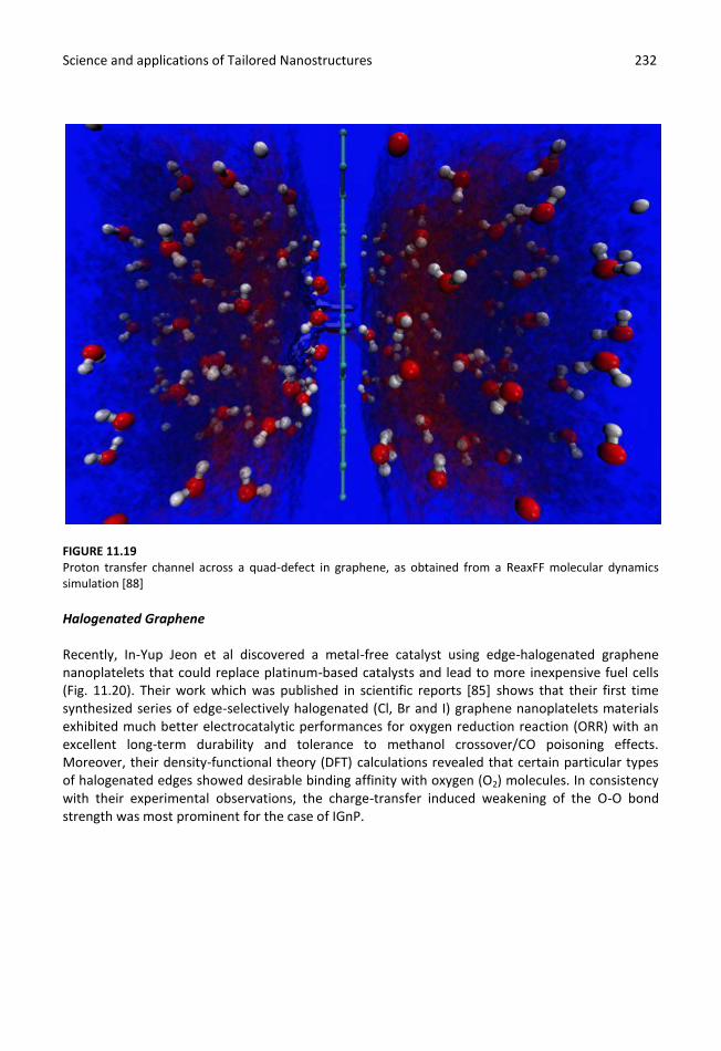
) [82], and its optical transmittance (~97.7%). These exciting properties make this carbon material a rising star in the world of nanomaterials and open the way to a large space of applications including sensors, transistors, terahertz imaging, composites, membranes, energy storage devices, batteries, and thin coatings for solar cells and LCD displays [83]. Owing to the versatility of graphene properties and projected applications, several production techniques were developed, ranging from the mechanical exfoliation of high quality grapheme to the direct growth on carbides or metal substrates and from the chemical routes using graphene oxide to the newly developed approach at molecular level [84]. Furthermore, graphene is increasingly explored as a possible platform for developing novel separation technologies. This interest has risen because it is a maximally thin membrane that, which once perforated with atomic accuracy, may allow ultrafast and highly selective sieving of gases, liquids, dissolved ions and other species of interest. In this frame, hydrogen is the lightest and most plentiful element on Earth and in our universe. So it shouldn’t be a big surprise that scientists are pursuing hydrogen as a clean, carbon-free, virtually limitless energy source for cars and for a range of other uses, from portable generators to telecommunications towers-with water as the only byproduct of combustion. Most recently, researchers employed this material in the field of fuel cells. The promise for nanomaterials in fuel cells has been a bit lackluster, until the latest discoveries of graphene’s potential. Imperfect Graphene A major challenge in fuel cell technology is efficiently separating protons from hydrogen. Defective single-layer graphene can produce a membrane that is the world's thinnest proton channel-only one atom thick. The thinness of the atom-thick graphene makes it a quick trip for the protons (Fig. 11.19). With conventional membranes, which are hundreds of nanometers thick, proton selection takes minutes much too long to be practical. Removing a few carbon atoms results in others being highly reactive, which starts the proton shuttling process. Only protons go through the tiny holes, making the membrane very selective.
[1]
Science and applications of Tailored Nanostructures 232 232
FIGURE 11.19 Proton transfer channel across a quad-defect in graphene, as obtained from a ReaxFF molecular dynamics simulation [88]
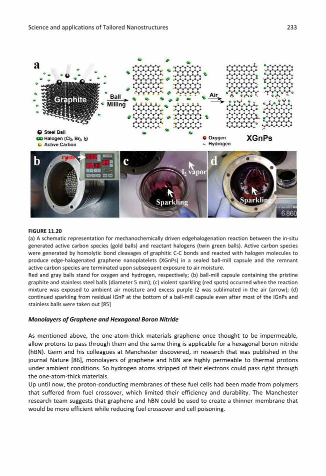
Halogenated Graphene Recently, In-Yup Jeon et al discovered a metal-free catalyst using edge-halogenated graphene nanoplatelets that could replace platinum-based catalysts and lead to more inexpensive fuel cells (Fig. 11.20). Their work which was published in scientific reports [85] shows that their first time synthesized series of edge-selectively halogenated (Cl, Br and I) graphene nanoplatelets materials exhibited much better electrocatalytic performances for oxygen reduction reaction (ORR) with an excellent long-term durability and tolerance to methanol crossover/CO poisoning effects. Moreover, their density-functional theory (DFT) calculations revealed that certain particular types of halogenated edges showed desirable binding affinity with oxygen (O2) molecules. In consistency with their experimental observations, the charge-transfer induced weakening of the O-O bond strength was most prominent for the case of IGnP.
Science and applications of Tailored Nanostructures 233 233
FIGURE 11.20 (a) A schematic representation for mechanochemically driven edgehalogenation reaction between the in-situ generated active carbon species (gold balls) and reactant halogens (twin green balls). Active carbon species were generated by homolytic bond cleavages of graphitic C-C bonds and reacted with halogen molecules to produce edge-halogenated graphene nanoplatelets (XGnPs) in a sealed ball-mill capsule and the remnant active carbon species are terminated upon subsequent exposure to air moisture. Red and gray balls stand for oxygen and hydrogen, respectively; (b) ball-mill capsule containing the pristine graphite and stainless steel balls (diameter 5 mm); (c) violent sparkling (red spots) occurred when the reaction mixture was exposed to ambient air moisture and excess purple I2 was sublimated in the air (arrow); (d) continued sparkling from residual IGnP at the bottom of a ball-mill capsule even after most of the IGnPs and stainless balls were taken out [85]
Monolayers of Graphene and Hexagonal Boron Nitride As mentioned above, the one-atom-thick materials graphene once thought to be impermeable, allow protons to pass through them and the same thing is applicable for a hexagonal boron nitride (hBN). Geim and his colleagues at Manchester discovered, in research that was published in the journal Nature [86], monolayers of graphene and hBN are highly permeable to thermal protons under ambient conditions. So hydrogen atoms stripped of their electrons could pass right through the one-atom-thick materials. Up until now, the proton-conducting membranes of these fuel cells had been made from polymers that suffered from fuel crossover, which limited their efficiency and durability. The Manchester research team suggests that graphene and hBN could be used to create a thinner membrane that would be more efficient while reducing fuel crossover and cell poisoning.
Science and applications of Tailored Nanostructures 234 234
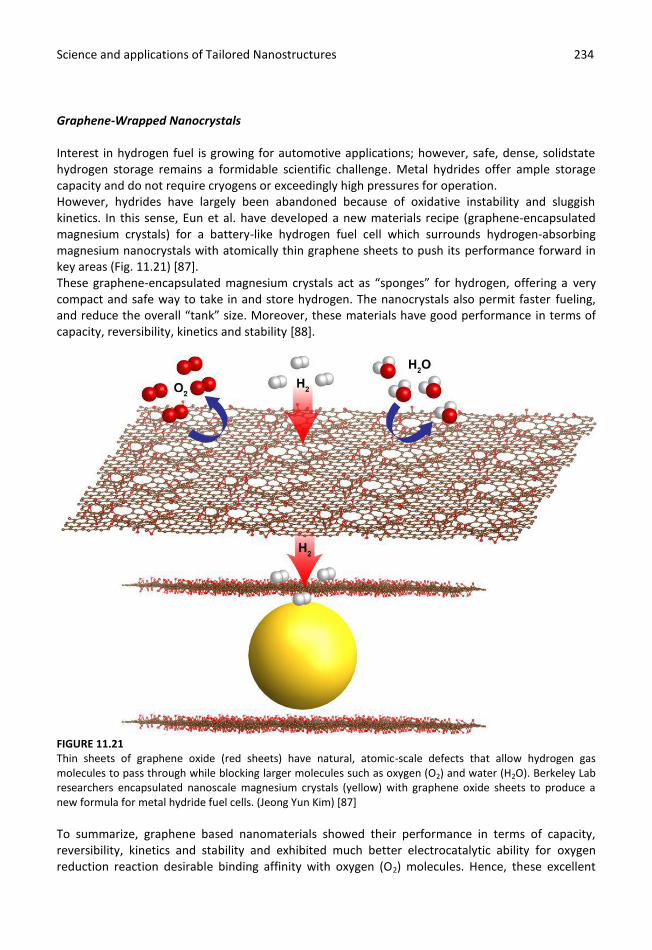
Graphene-Wrapped Nanocrystals Interest in hydrogen fuel is growing for automotive applications; however, safe, dense, solidstate hydrogen storage remains a formidable scientific challenge. Metal hydrides offer ample storage capacity and do not require cryogens or exceedingly high pressures for operation. However, hydrides have largely been abandoned because of oxidative instability and sluggish kinetics. In this sense, Eun et al. have developed a new materials recipe (graphene-encapsulated magnesium crystals) for a battery-like hydrogen fuel cell which surrounds hydrogen-absorbing magnesium nanocrystals with atomically thin graphene sheets to push its performance forward in key areas (Fig. 11.21) [87]. These graphene-encapsulated magnesium crystals act as “sponges” for hydrogen, offering a very compact and safe way to take in and store hydrogen. The nanocrystals also permit faster fueling, and reduce the overall “tank” size. Moreover, these materials have good performance in terms of capacity, reversibility, kinetics and stability [88].
FIGURE 11.21 Thin sheets of graphene oxide (red sheets) have natural, atomic-scale defects that allow hydrogen gas molecules to pass through while blocking larger molecules such as oxygen (O2) and water (H2O). Berkeley Lab researchers encapsulated nanoscale magnesium crystals (yellow) with graphene oxide sheets to produce a new formula for metal hydride fuel cells. (Jeong Yun Kim) [87]
To summarize, graphene based nanomaterials showed their performance in terms of capacity, reversibility, kinetics and stability and exhibited much better electrocatalytic ability for oxygen reduction reaction desirable binding affinity with oxygen (O2) molecules. Hence, these excellent
Science and applications of Tailored Nanostructures 235 235
properties make one-atom-thick crystals promising candidates for use in many fuel cells technologies.
Acknowledgement The work was supported by funds coming from National Research foundation of South Africa, and the department of science and technology of South Africa.
References
1. A.B. Markman, K.L. Wood, Tools for innovation; the science behind the practical methods that drive new ideas, 2009, oxford university press, New York.
2. A.B. Arons, M.B. Peppard, Am. J. Phys. 33 (5) (1965) 367. 3. T. Mueller, Dissertation, 2009, University of Hagen, Germany. 4. G.C. Papageorgiou, Govindjee, Chlorophyll a Fluorescence; a signature of photosynthesis,
2004, Springer, Netherlands. 5. M. Shukuya, Energy; Theory and applications in the built environment, 2013, Springer,
London. 6. Home of graphene, http://www.graphene.manchester.ac.uk/explore/the-story-of-
graphene/ (19 March 2016). 7. Z. Liu, X. Zhou, Graphene; energy storage and conversion applications, 2015, CRC press,
USA. 8. K.J. Klabunde, R.M. Richards, Nanoscale Materials in Chemistry, 2nd Ed, 2009, John Wiley
and sons, New Jersey. 9. ShayoNano, http://shayonano.com/faq/ (19 March 2016). 10. R.P. Feynman, Am. Phys. Soc. December, (1959). 11. Z.L. Wang, Mater. Today, 7 (2004) 26. 12. Q.X. Zhao, P. Klason ,M. Willander, Appl. Phys. A, 88 (2007) 27. 13. R. Barman, S.K. Singh, D. Kaur, , Thin Solid Films, 594 (2015) 80. 14. C. Mattevi, H. Kim, M. Chhowalla, J. Mater. Chem. 21 (2011) 3324. 15. F.V. Molefe, L.F. Koao, B.F. Dejene, H.C. Swart, Opt. Mater. 46 (2015) 292. 16. A.M. Elnahrawy, Y.O. Kim and A.I. Ali, J. Alloys Compd. 676 (2016) 432. 17. X. Ye, C. Zheng, L. Ma. X. Huang, Microemulsion-assisted hydrothermal preparation and
infrared radiation property of Ti 2 O nanomaterials with tunable morphologies and crystal form, Mater. Sci. Semicond. Process. 31 (2015) 295.
18. J. Behari, Indian J. Exp. Biol. 48 (2010) 1008. 19. R. Overney, Nanothermodymics and Nanoparticle Synthesis,
http://courses.washington.edu/overney/NME498_Material/NME498_Lectures/Lecture%20on%20Thermo%20and%20Nanoparticles%20v5.pdf (22 May 2016).
20. E. Roy, S. Patra, A. Tiwari, R. Madhuri, P.K. Sharma, Biosens. Bioelectron. (2016) 1. 21. J.C.G. Bünzli, A.S. Chauvin. Lanthanides in Solar Energy Conversion. In Handbook on the
Physics and Chemistry of Rare Earths, Vol. 44, (2014), Netherlands. 22. F.V Molefe, L.F. Koao, J.J. Dolo and B.F. Dejene, Physica B 439 (2014) 185.
Science and applications of Tailored Nanostructures 236 236
23. Z. Liang, Q. Zhang, O. Wiranwetchayan, J. Xi, Z. Yang, K. Park, C. Li, and G. Cao, Adv. Funct. Mater. 22 (2012) 2194.
24. J. Das, D.K. Mishra, V.V. Srinivasu, D.R. Sahu, B.K. Roul, J. Mag. Mag. Mat. 382 (2015) 111. 25. V. Kumar, V. Kumar, S. Som, L.P. Purohit, O.M. Ntwaeaborwa and H.C. Swart, J. Alloys
Comp. 594 (2014) 32. 26. B.J. Monn, K.S. Lee, J. Shim, S. Park, S.H. Kim, Bae, M. Park, C.-L. Lee, W.K. Choi. Y. Yi, J.Y.
Hwang and D.I. Son, Nano Energy 20 (2016) 221. 27. K. Park, Q-F. Zang, D. Myers and G.Z. Cao, ACS Appl. Mater. Interface 5 (2013) 1044. 28. D.B. Hall, P. Underhill and J.M. Torkelson, Polym. Eng. Sci. 38 (1998) 2039. 29. C.S. Kumara Ranasinghe, E.N. Jayaweera, G.R.A. Kumara, R.M.G. Rajapakse, Herath
Mudiyanselage Navarathna Bandara, Masamichi Yoshimura, J. Mater. Sci. Eng. A, 5, (2015) 361.
30. S.L. Holl, C.A. Colinge, S. Song, R. Varasala, K. Hobart and F. Kub, 3 (2006) 67. 31. M. Singh, T.R. Rana, J.H. Kim, J. Alloys Compd. 675 (2016) 370. 32. S.A. Kandjani, S. Mirershadi, A. Nikniaz, Sol. Cells - New Approaches Rev. (2015) 223. 33. NobelPrize, http://www.nobelprize.org/nobel_prizes/physics/laureates/2014/press.html
(20 March 2016). 34. https://www.ecse.rpi.edu/~schubert/Light-Emitting-Diodes-dot-org/chap21/F21-
07%20Nichia%20wh%20LED%20structu.jpg (20 March 2016). 35. X. Zhang, W. Liu, G.Z. Wei, D. Banerjee, Z. Hu, J. Li, J. Am. Chem. Soc. 136 (40) (2014) 14230. 36. http://www.hzkjzx.org.cn/upfiles/20111017154716763.jpg (21 June 2016). 37. M.S. Dhlamini, Thesis, 2008, University of the Free State, South Africa. 38. C. de Mello Donega, Chem. Soc. Rev. 40 (2011) 1512. 39. S.S. and N. S. Saricifti, Organic Photovoltaics, Mechanisms, Materials and devices, (2005)
Johannes Kepler University of Linz, Austria. 40. E.S. Aydil, Nanomaterials for Solar Cells, Nanotechnology Law and Business 4 (2007) 275. 41. http://library.thinkquest.org/06aug/01335/welcome.htm (11 Nov 2011). 42. PV Technology Industry Roadmap Workshop Report, website: www.nrel.gov/ncpv (11 Nov
2011). 43. G.P. Willek, The Crystalline Silicon Solar Cell, History, Achievements and Perspectives, 19th
European PV Solar Energy Conference, June 2004, Paris, France. 44. M.A. Green, Silicon Solar Cells, Evolution, High efficiency Design and Efficiency
Enhancements, Semiconductor Science and Technology, 8(1993) 1. 45. G. Ghidichimo and L. Filippelli, Organic Solar Cells: Problems and Perspectives,
International Journal of Photoenergy, May 2010, doi:10.1155/2010/123534. 46. S. Gunes and N.S. Sariciftci, Inorganica Chimica Acta 361(2008) 581. 47. T.Y. Chu, S.W. Tsang, J. Zhou, P.G. Verly, J.P. Lu, S.Beaupre, M. Leclerc and Y. Tao, Solar
Energy Materials and Solar Cells (2011), doi:10.1016/j.solmat.2011.09.042. 48. http://www.nrel.gov/ncpv/images/efficiency_chart.jpg (11 Nov 2011). 49. L.M. Chen, Z. Hong, G. Li and Y. Yang., Advanced Materials 21(2009) 1434. 50. J. Peet, C. Soci, R. C. Coffin, T. Q. Nguyen, A. Mikhailovsky, D. Moses, G.C. Bazan, Applied
Physics Letters 89(2006) 252105. 51. C. Soci, I.W. Hwang, D. Moses, Z. Zhu, D. Waller, R. Gaudiana, C. J, Brabec, A. J. Heeger,
Advanced Functional Materials 17(2007) 632. 52. H. Oh, J. Krantz, I. Litzov, T. Stubhan, L. Pinna and C.J. Brabec, Solar Energy Materials and
Solar Cells 95 (2011) 2194. 53. N. Sekine, C.H. Chou, W.L Kwan and Y. Yang, Organic Electronics 10 (2009) 1473.
Science and applications of Tailored Nanostructures 237 237
54. S.H Eom, S. Senthilarasu, P. Uthirakumar, C.H. Hong, Y.S. Lee, J. Lim, S. C Yoon, C. Lee and S.H. Lee, Solar Energy Mater. Solar Cells 92 (2008) 564.
55. S.R. Cowan, N. Banerji, W.L. Leong and A.J. Heeger, Advanced Functional Materials, 22 (2012) 1116.
56. B. Zhang, D.H. Lee, H. Chae, C. Park and H.-M. Cho, Korean Journal of Chemical Engineering, 27 (2010) 999.
57. A. Manzano-Ramírez, E.J. López-Naranjo, W. Soboyejo, Y. Meas-Vong, B. Vilquin, J. Nanomaterials 2015 (2015) 15.
58. L. Qian, J. Yang, R. Zhou, A. Tang, Y. Zheng, T.-K. Tseng, D. Bera, J. Xue and P. H. Holloway, Journal of Materials Chemistry, 21 (2011) 3814.
59. http://www.clean.cise.columbia.edu/process/spintheory.pdf (November 2012). 60. http://www.google.co.za/search?q=Diagram+of+vacuum+evaporator (November 2012). 61. http://www.clean.cise.columbia.edu/process/spintheory.pdf (November 2012). 62. H. Spanggaard and F.C Krebs, Solar Energy Mater. Solar Cells 83 (2004) 125. 63. M. Jorgensen, K. Norrman, F.C. Krebs, Solar Energy Mater. Solar Cells 92 (2008) 686. 64. B.E McCandless and S.S Hegedus, Proceedings of the 22nd IEEE Photovoltaic Specialists
Conference (1991) 967. 65. J. Sterner, Comprehensive Summaries of Uppsala Dissertations from the Faculty of Science
and Technology, 942 (2004) 14. 66. S. Tachikawa, A. Nogushi, T. Tsuge, M. Hara, O. Odawara and H. Wada, Materials, 4 (2011)
1132. 67. Y. Zhao, Z. Xie, Y. Qu, Y. Geng and L. Wang, Synthetic Metals, 158 (2008) 908. 68. T.L. Benanti and D. Venkataraman, Photosynthesis Research, 87 (2006) 73. 69. P.S. Mbule, H.C. Swart, O.M. Ntwaeaborwa, J. Colloi Interface Sci. 436 (2014) 9. 70. L.L. Noto, Masters Thesis, University of the Free State, 2011. 71. L.L. Noto, PhD Thesis, University of the Free State, 2014. 72. http://shop.walkerart.org/products/glow-brick-suck-uk (20 March 2016). 73. V. Pagonis, G. Kitis, C. Furetta, Numerical and practical exercises in thermoluminescence,
2006, Springer and business Media Inc. USA. 74. A.J.J. Bos, Radiation Measurement 41 (2007) S45. 75. P.R. Gonzales, C. Furetta, E. Cruz-Zaragoza, J. Azorin, Mod. Phys. Lett. B, 4 (8), (2010) 717. 76. I. Veronese, The thermoluminescence peaks of quarts at intermediate temperatures and
their use in dating and dose reconstruction [Thesis], 2005, UniversitaDegliStudi Milano. 77. L. Bøtter-Jensen, S.W.S. McKeever, A.G. Wintle, Optically Stimulated Luminescence
Dosimetry, 2003, Elsevier, Amsterdam. 78. Geim, A.K. and Novoselov, K.S. (2007) Nat. Mater. 6, 183.
http://dx.doi.org/10.1038/nmat1849. 79. K.I. Bolotin, K.J. Sikes, Z. Jiang, , M. Klima, G. Fudenberg, J. Hone , P. Kim, H.L. Stormer,
(2008) Solid Stat. Comm. 146 (2008) 351. 80. S.V. Morozov, K.S. Novoselov, , M.I. Katsnelson, , F. Schedin, D.C. Elias, J.A. Jaszczak, A.K.
Geim, Physical Review Letters (2008) 100, Article ID: 016602. http://dx.doi.org/10.1103/PhysRevLett.100.016602.
81. C. Lee, X.D. Wei, J.W. Kysar, J. Hone, (2008) Science, 321 (2008) 385. 82. A.A. Balandin, , S. Ghosh, W.Z. Bao, , I. Calizo, , D. Teweldebrhan, , F. Miao, C.N. Lau, Nano
Letters, 8 (2008) 902. 83. R. Ruoff, (2008) Graphene: Calling All Chemists. Nature Nanotechnology, 3 (2008) 10.84.

Science and applications of Tailored Nanostructures 238 238
84. S. Caterina, M. Ather, D. Erik, (2010) Production, Properties and Potential of Graphene. Carbon, 48 (2010) 2127.
85. I.Y. Jeon, H.J. Choi, M. Choi, J.M. Seo, S.M. Jung, M.J. Kim, S. Zhang, L. Zhang, Z. Xia, L. Dai, N. Park, J.B. Baek, Scientific reports. 3, 2013, doi:10.1038/srep01810.
86. S. Hu, M. Lozada-Hidalgo, F. C. Wang, A. Mishchenko, F. Schedin, R. R. Nair, E. W. Hill, D. W. Boukhvalov, M. I. Katsnelson, R. A. W. Dryfe, I. V. Grigorieva, H. A. Wu, A. K. Geim, Nat. 516 (2014) 227.
87. E.S. Cho, A.M. Ruminski, S. Aloni, Y.S. Liu, J. Guo, J.J. Urban, Nat. Comm. 7, 2016, doi:10.1038/ncomms10804.
88. J. L. Achtyl, R. R. Unocic, L. Xu, Y. Cai, M. Raju, W. Zhang, R. L. Sacci, I. V. Vlassiouk, P. F. Fulvio, P. Ganesh, D. J. Wesolowski, S. Dai, A. C. T. van Duin, M. Neurock & F. M. Geiger, Nat. Comm. 6 (2015) 1.