Embed Size (px)
Citation preview

Journal of Materials Science Research; Vol. 5, No. 1; 2016 ISSN 1927-0585 E-ISSN 1927-0593
Published by Canadian Center of Science and Education
61
Nanotechnology: A Journey towards Finding Solutions Satya Pal Singh1
1 Department of Applied Sciences, Madan Mohan Malaviya University of Technology, Gorakhpur, UP, India Correspondence: Satya Pal Singh, Department of Applied Sciences, Madan Mohan Malaviya University of Technology, Gorakhpur, UP, India. E-mail: [email protected], [email protected] Received: October 26, 2015 Accepted: November 9, 2015 Online Published: December 23, 2015
doi:10.5539/jmsr.v5n1p61 URL:http://dx.doi.org/10.5539/jmsr.v5n1p61 Abstract Nanotechnology is the understanding and control of matter at the diemnsions ranging between 1-100 nm. One nanometer is one billionth of a meter. Nanotechnology involves manipulation of atoms, imaging, measuring and modelling at nano scale. Its potentials were first highlighted by Richard Feynman in the American Physical Scociety meeting in 1959. Though, he did not coin the world nanotechnology himself but he explored the possiblities of functional materials at the bottom of the scale. In last two decades this technology has been commercialized to great extent and gaining importance day by day influencing the economies of different countries and henceforth enforcing the policy makers to address the issues like environment, health and safety. Governments are regularisaing and monitoring its research, uses, applications and technology transfer which includes intelluctaul property rights. This paper addresses the dimensions and trends of nanotechnology covering economic aspects. The paper is focussed on the changes in the functional properties of nanomaterials as physical, chemical, optical, electronic, electrical, magnetic etc. in comparision to those of the bulk of material. It has been discussed how the basic and advance research in nanoscience could be explotiedfor making technologies for its commercial and industrial applications for the benefit and safety of the soceity. Thin film magnetism is demonstrated using Monte Carlo simulation method. Experimental synthesis of some of the nanorods and qunatum dots are also discussed. 1. Introduction According to USA National Nanotechnology Initiative mission variuos aspects of nanotechnology can be encapsulated in the definition-“ The essence of nanotechnology is the ability to work at the molecular level, atom by atom, to create large structures with fundamentally new molecular organiziation. Behavior of structural features with a typical dimension in the range of 1-100 nm (i.e . 1000 times smaller than the diameter of the human hair) exhibit important changes in comparison to those of the bulk of the materials. Nanotechnology is concerned with materials and systems whose components and systems exhibit novel and significantly improved physical, chemical and biological properties, phenomena and processes due to their nanoscale size. The goal is to exploit these properties by gaining control of structures and devices at atomic, molecular and supramolecular levels and to learn efficiently manufacture and use these devices.”(National Nanotechnology Initiative, 2000) In word nanoscience the prefix nano has the Greek origin which means “dwarf”. A nanomaterial is defined as a material which as atleast one of its three dimensions in the range of 1-100 nm. The electrical, optical and elctronic properties of nanomaterials are changed drastically because of the fact that these materails are composed only of few hundreds of molecules. In a loose sense, one can say that these materials may allow electron conduction with more ease because of the absence of the bulk of the materials. The assembly of only few hundreds of molecules have a different band gap than those of atoms in a bulk of material altering the semiconducting properties. These bands also changes their optical response. Manipulation of atoms and molecules at nanoscale can help us to bring desired change inproerpties of our interest. CNT, MWCNT and C60 (i.e. fullerene) doped with atoms of Khave been widely used as nanomaterials for their electrical as well as mechanical properties(Poole & Owenes, 2009). The number of atoms on surface in comparison tothose of the whole volume is also very high in the case of nanomaterials which allows for better chemical and catalytic reactions. This happens because of having more number of active sites. As for example for a FCC nanoparticle of n layers, the total number of atoms in nanoparticle is given by- =[10 − 15 + 11 − 3] where as those on the surface is given by- = [10 − 20 + 12](Poole & Owenes, 2009). There exist three generic types of nanostructures- 1. Zero-dimensional (0D) systems (Quantum dots) 2. One-dimensional (1D) systems (Qunatum wires) and 3. Two-dimensional (2D) systems (Quantum well).
www.ccsenet.org/jmsr Journal of Materials Science Research Vol. 5, No. 1; 2016
62
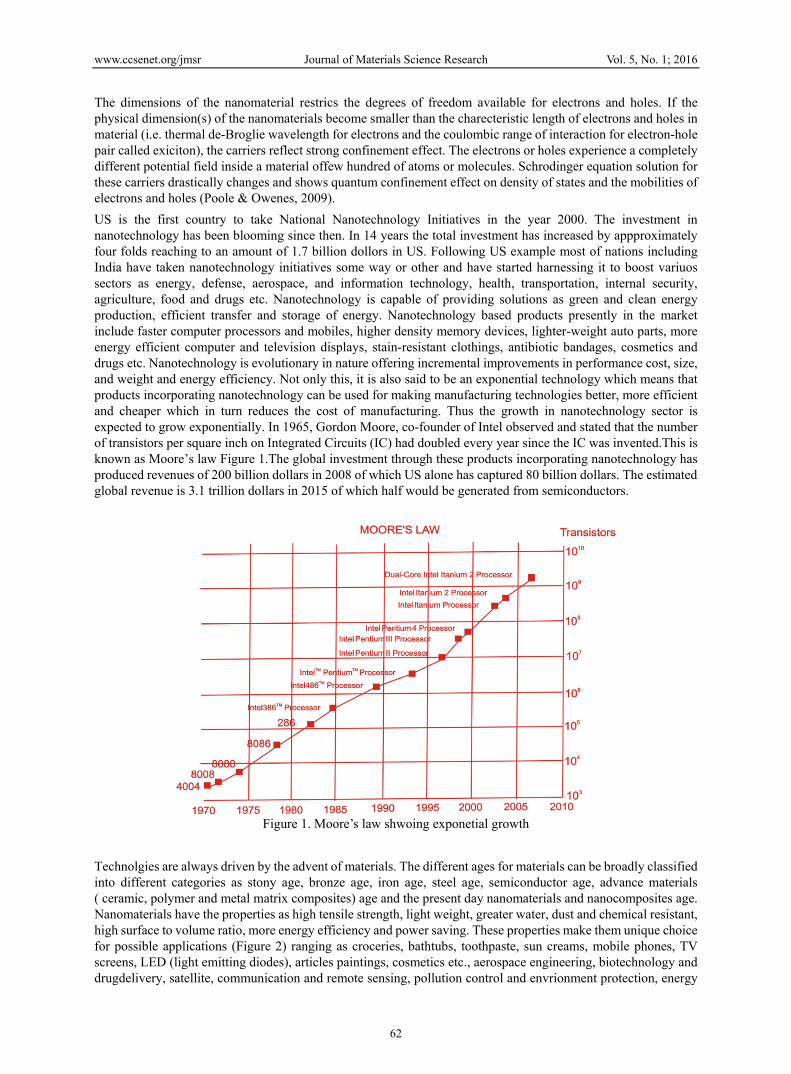
The dimensions of the nanomaterial restrics the degrees of freedom available for electrons and holes. If the physical dimension(s) of the nanomaterials become smaller than the charecteristic length of electrons and holes in material (i.e. thermal de-Broglie wavelength for electrons and the coulombic range of interaction for electron-hole pair called exiciton), the carriers reflect strong confinement effect. The electrons or holes experience a completely different potential field inside a material offew hundred of atoms or molecules. Schrodinger equation solution for these carriers drastically changes and shows quantum confinement effect on density of states and the mobilities of electrons and holes (Poole & Owenes, 2009). US is the first country to take National Nanotechnology Initiatives in the year 2000. The investment in nanotechnology has been blooming since then. In 14 years the total investment has increased by appproximately four folds reaching to an amount of 1.7 billion dollors in US. Following US example most of nations including India have taken nanotechnology initiatives some way or other and have started harnessing it to boost variuos sectors as energy, defense, aerospace, and information technology, health, transportation, internal security, agriculture, food and drugs etc. Nanotechnology is capable of providing solutions as green and clean energy production, efficient transfer and storage of energy. Nanotechnology based products presently in the market include faster computer processors and mobiles, higher density memory devices, lighter-weight auto parts, more energy efficient computer and television displays, stain-resistant clothings, antibiotic bandages, cosmetics and drugs etc. Nanotechnology is evolutionary in nature offering incremental improvements in performance cost, size, and weight and energy efficiency. Not only this, it is also said to be an exponential technology which means that products incorporating nanotechnology can be used for making manufacturing technologies better, more efficient and cheaper which in turn reduces the cost of manufacturing. Thus the growth in nanotechnology sector is expected to grow exponentially. In 1965, Gordon Moore, co-founder of Intel observed and stated that the number of transistors per square inch on Integrated Circuits (IC) had doubled every year since the IC was invented.This is known as Moore’s law Figure 1.The global investment through these products incorporating nanotechnology has produced revenues of 200 billion dollars in 2008 of which US alone has captured 80 billion dollars. The estimated global revenue is 3.1 trillion dollars in 2015 of which half would be generated from semiconductors.
Figure 1. Moore’s law shwoing exponetial growth
Technolgies are always driven by the advent of materials. The different ages for materials can be broadly classified into different categories as stony age, bronze age, iron age, steel age, semiconductor age, advance materials ( ceramic, polymer and metal matrix composites) age and the present day nanomaterials and nanocomposites age. Nanomaterials have the properties as high tensile strength, light weight, greater water, dust and chemical resistant, high surface to volume ratio, more energy efficiency and power saving. These properties make them unique choice for possible applications (Figure 2) ranging as croceries, bathtubs, toothpaste, sun creams, mobile phones, TV screens, LED (light emitting diodes), articles paintings, cosmetics etc., aerospace engineering, biotechnology and drugdelivery, satellite, communication and remote sensing, pollution control and envrionment protection, energy

www.ccsenet.org/jmsr Journal of Materials Science Research Vol. 5, No. 1; 2016
63
and data storage, fast computing processors and weapons and agroproducts (National Nanotechnology Initiative, 2000). Nano-motors, bio-senors, bio-photonic devices, spintronic, photonic and mechanical (i.e. nano electromechanical systems NEMS) devices have emerged as recent thrust areas of naotechnology. Nanomaterial based devices and instruments are widely being used for the prification of water. The waste water treatment becomes mandatory for the reasons well known. The industrial waste water can cause heart, lungs and skin diseases. It has been observed to cause cancer among routine users. The industries like cement, leather and tanning produce waste water containing metals and other harmful chemicals. Many of these are toxic and harmful to living being.
Figure 2. Applications of Nanotechnology
Nanomaterials as Zeolite,Carbon Nano Tubes (CNTs), very thin membranes and other mesoporous materials have been used for separation,filtration and removal of meatls as Cr, As etc from contaminated water (Wang & Lo, 2009; Rana, Mohan, & Rajagopal, 2004; Gupta & Ali, 2004; Ali & Gupta, 2006; Gupta, Gupta, & Sharma, 2001; Singh, Gupta, & Gupta, 2007; Shevade & Ford, 2004; Rengaraj, Choi, & Yi, 2004; Singh, 2014). Cr(VI) is adsorbed by CNTs and is separated from containimated water but reusing CNTs have been a challenge. Recently, - A novel idea has been discussed and presented for recycling such CNTs in Singh (2014). The issue of interest is that whether the in and out vitro cleansing of adsrobed Cr(VI) from such CNTs can be achieved by flowing these CNTs in a narrow streamline jet of some fluid of interest inside a channel (Singh, 2014). Not ony that the molecular level tweaking force or exertions at CNTs surface can be produced using ultrasonic transducers by producing alternate denser and rarer regions inside medium (i.e. accoustic grating) Figure 3. This may be technologically very challenging because of the fact that the precision and control required is of the molecular scale (Singh, 2014).
Figure 3. A novel mechanism to produce tweaking molecular forces fro cleansing of CNTs and re-cycling
www.ccsenet.org/jmsr Journal of Materials Science Research Vol. 5, No. 1; 2016
64
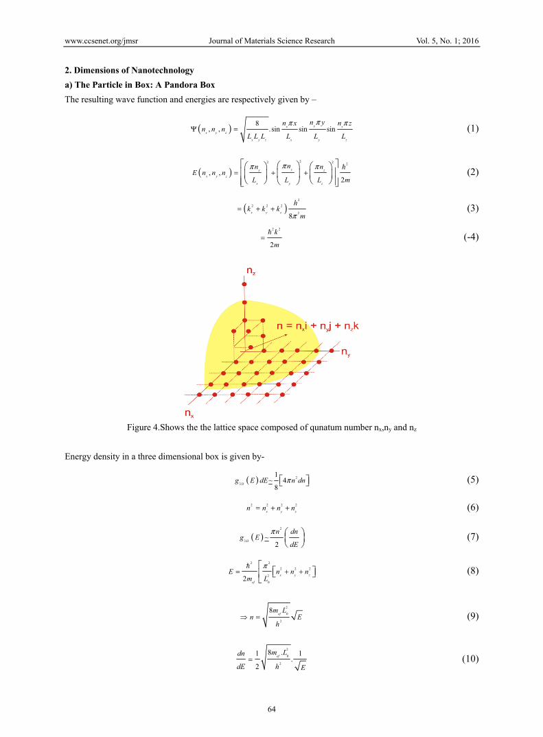
2. Dimensions of Nanotechnology a) The Particle in Box: A Pandora Box The resulting wave function and energies are respectively given by –
( ) 8, , .sin sin sinyx z
x y z
x y z x y z
n yn x n zn n n
L L L L L L
ππ πΨ = (1)
( )22 2 2
, ,2
yx z
x y z
x y z
nn nE n n n
L L L m
ππ π= + +
(2)
( )
22 2 2
28x y z
hk k k
mπ= + +
(3)
2 2
2
k
m=
(-4)
Figure 4.Shows the the lattice space composed of qunatum number nx,ny and nz
Energy density in a three dimensional box is given by-
( ) 2
3
1~ 4
8Dg E dE n dnπ (5)
2 2 2 2
x y zn n n n= + + (6)
( )2
3~
2D
n dng E
dE
π
(7)
2 2
2 2 2
2
02 x y z
ef
E n n nm L
π= + +
(8)
2
0
2
8ef
m Ln E
h = (9)
2
0
2
8 .1 1.
2ef
m Ldn
dE h E= (10)

www.ccsenet.org/jmsr Journal of Materials Science Research Vol. 5, No. 1; 2016
65
3
22
0
3 2
8 .( ) .
4ef
D
m Lg E E
h
π−
(11)
The density of states is defined by dividing )(3 Eg D by the physical volume of the box-
3
22
0
2
8 .(3 ) .
4ef
energy
m LD E
h
πρ −
(12)
Figure 5. Quantum Dots with gradually stepping emission from violet to deep red. Just by taking dimensions of few nanometers one can see that energy states of the electrons under such confinement becomes as high as to form
Plasmon which scatter light in this fashion Source: https://en.wikipedia.org/wiki/Quantum_dot#
b) Particle in a Two Dimensional Box- Repeating similar exercise but in two dimension, we can write-
3
22
0
2
8 .(3 ) .
4ef
energy
m LD E
h
πρ −
(13)
( )21( ) 24dg E dE n dnπ− (14)
22 20
2 20
88 .
ef
ef
m Ln hE n Em L h
= = (15)
20
2
81 1.2
efm LdndE h E
= (16)
20
2 2
2( ) ef
D
m Lg E
hπ
− (17)

www.ccsenet.org/jmsr Journal of Materials Science Research Vol. 5, No. 1; 2016
66
Figure6. Shows the the lattice space composed of qunatum number nx,ny in 2 dimensions Density of states is obtained by dividing the physical volume of the system-
2
2(2 ) ef
energy
mD
hπ
ρ − (18)
Density of states as obtained for a particle in a two dimensional box is a constant.
(a) (b) Figure 7. a) Shows the density of states vs E for different type of materials b) Shows the one dimensional density of
states for (8,8), (9,9), (10,10) and (11,11) armchair carbon nanotubes
c) Particle in a One Dimensional Box- The energy of the particle is given by –
www.ccsenet.org/jmsr Journal of Materials Science Research Vol. 5, No. 1; 2016
67
2 2 2 2
20 28 efef
n h kEmm L
= = (19)
0/k n Lπ= (20)
20
2
8 efm Ln E
h= (21)
1 ( )Dg E dE dn− (22)
1 ( )Ddn ng EdE E
Δ− −Δ
(23)
20
1 2
81 1( ) .2
efD
m Lg E
h E− (24)
2
2 11 efenergy
mD
h Eρ = (25)
3. Trends of Nanotechnology Though, the importance of assembling atoms at nanoscales was first highlighted by famous physicist Prof. Richard Feynman in a meeting of American Physical Society on 29th December 1959 at Caltech, it is still estimated to be an emerging area in general from the point of view of the developments in the area of nanotechnology. We can group different countries in three categories on the basis of their achievements and advancement in this area- National Activity Nations, Current R & D Empowerment Nations and Demonstration of Interest Nations. USA, China, Japan and Russia are the major players in National Activity Nations. Countries like India, Brazil, Malaysia, Thailand, Singapore and South Africa are at Current R & D Empowerment Scale. Many other countries which have started their Nano initiative programs are at the lowest level of Demonstration of Interest Stage.
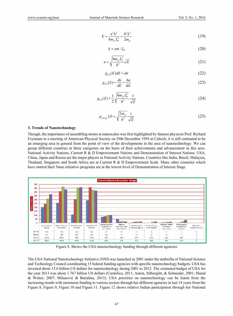
Figure 8. Shows the USA nanotechnology funding through different agencies
The USA National Nanotechnology Initiative (NNI) was launched in 2001 under the umbrella of National Science and Technology Council coordinating 15 federal funding agencies with specific nanotechnology budgets. USA has invested about 15.6 billion US dollars for nanotechnology during 2001 to 2012. The estimated budget of USA for the year 2013 was about 1.767 billion US dollars (Cientifica, 2011; Anton, Silberglitt, & Schneider, 2001; Shand & Wetter, 2007; Milanović & Bučalina, 2013). USA priorities on nanotechnology can be learnt from the increasing trends with enormous funding to various sectors through her different agencies in last 14 years from the Figure 8, Figure 9, Figure 10 and Figure 11. Figure 12 shows relative Indian participation through her National
www.ccsenet.org/jmsr Journal of Materials Science Research Vol. 5, No. 1; 2016
68
Nano-initiative program. Figure 13 reflects that nano-enabled drug delivery have captured the market share to a reasonable extent and it will grow exponentially in coming future. That also reflects that nano-enabled drugs are more effective to cure from diseases because of its increasing demand in the market.
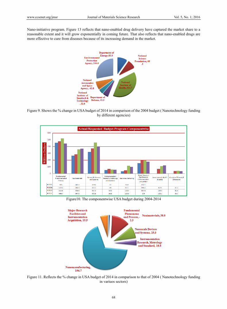
Figure 9. Shows the % change in USA budget of 2014 in comparison of the 2004 budget ( Nanotechnology funding
by different agencies)
Figure10. The componentwise USA budget during 2004-2014
Figure 11. Reflects the % change in USA budget of 2014 in comparison to that of 2004 ( Nanotechnology funding
in variuos sectors)

www.ccsenet.org/jmsr Journal of Materials Science Research Vol. 5, No. 1; 2016
69
Figure12. Shows the ratio of the estimated nanotechnology funding in comaprison to that of Indian budget
allocation by various National Activity Nations in 2004
Figure 13. Global marketshare and market volume of nano-enabled drug delivery (Ezema, Ogbobe, & Omah,
2014) India started her Nanoscience and Technology Initiative (NSTI) actively in her five year plan of 2007-2012 with an estimated budget of Rs. 1000.0 crores (The Energy and Resources Institute (TERI), 2010). This was aimed to establish center of excellence, targeting laboratories, infrastructure and human resource development in strong collaboration with foreign partners as USA, UK, Germany, Japan and Russia. A more specific detail of nano-initiative programs of many other countries as Japan, China, Russia (National Activity Group), Brazil, Malaysia, Thialand, Singapore and South Africa (Current R & D and Empowerment Scale) can be obtained in research paper (Ezema, Ogbobe, & Omah, 2014) and its refrences.
4. Methoddology and the investigations: a) Synthesis, Characterization and Nanometrology From earlier discussions, it is clear that nanotechnology gained econmic importance only few decades back. The reasons have purely scientific origins andcan be learnt in this section. Though, Feynman’s visionary ideas on nanotechnology goes back to 1959 but there was little progress in that direction till 1981.That is the year which marked the invention of Scanning Tunneling Microscope (STM). STM was invented by a group of scientists led by Gerd Binnig and Heinrich Rohrer at IBM Zurich Research Laboratory. They published the first STM image of the Si(III)-7 x 7 surface in 1983 (Shong, Sow, & Wee, 2010). Gerd Binnig and Heinrich Rohrer shared the Nobel prize in physics in 1986 for their invention of STM. The Atomic Force Microscope (AFM) was invented in 1986. These two inventions have made greatest impact in the field of nanoscience and nanotechnology. Various top down and

www.ccsenet.org/jmsr Journal of Materials Science Research Vol. 5, No. 1; 2016
70
bottom up approaches (i.e. Chemical Vapor deposition (CVD), Molecular Beam Epitaxy (MBE), Colloidal method, Sol-gel method, Spin costingetc.) were developed in due course of time which definitely depended on the scientific progress in the area of nanometrology. The objectives of the nanometrology is to providecoordinates and identity of every constituent atoms in a nanostructured material, object or nanodevice. The important techniques and tools which play vital role in nanometrology can be listed as – X-rays diffraction (XRD), Atomic Force Microscope (AFM), Scanning Tunneling Microscope (STM), Transmission Electron Microscope (TEM) etc. The optical techniques for characterizing surface regularity are Ellipsometry, Scanning Angle Reflectometry (SAR), Surface Plasmon Resonance (SPR), Optical Waveguide Lightmode Spectroscopy (OWLS) etc (Shong, Sow, & Wee, 2010). The new developments and the modifications in these instuments and techniques after STM have helped scientists and engineers to manipulate, control and engineer materials and structures at nanoscale to great extent in last few decades.
Figure 14. a) TEM micrographs fro nickel oxalate dihydrate synthesised usin a) CTAB/1-butanol/1-hexane and b)
Tergito/1-octanol/cyclohexane Reprodcued by permission from (Ganguli, 2010)
Figure 15 a) Shows the ray-sketch for synthesis Cd-Se quantum dots b) Shows the nucleation and crystal growth (CdMe2and Trioctylphosphine selenide are respectively usedas metal and chalcogen precursors)

www.ccsenet.org/jmsr Journal of Materials Science Research Vol. 5, No. 1; 2016
71
The applications of nanoscale phenomena could start taking place only few decades back. I give you one example. The influence of spin on electron conductivity was first proposed by Nevill Mott in 1936 but it could be expoited for technological applications only after the discovery of Giant Magneto-Resistance (GMR) in 1988 (Ramsden, 2011). The discovery of GMR led to the barnch of spinotronics. It can be defined as the technology in which electron spin interplays with other properties of material as conductivity. To observe the phenomenon of GMR two ferromagnetic ultra thin films are separted by athin non-magnetic Fe or Cr film. There exists a ferromagnetic or antiferromagnetic interaction between the magnetic layers depending on the width of Cr or Fe layer which separates the two magnetic superlattices. The antiferromagnetic state of the magnetic layers can be transformed back into the ferromagnetic state by an external magnetic field.The spin dependent scattering of the conduction electrons in non-magnetic layer cause a small resistance when spin alligns parallel in two films where as for anti-parallel spin allignment of spins in two separted films, the resistance is high. This technology is being used for read-write heads in computer hard drives. This type of highly polarized spin transport could be demonstrated as GMR and could be exploited for technological applications only after the development of methods for synthesis of high qulaity ultra-thin films of thickness <100 nm (Ramsden, 2011). b) Computational Modelling Computational modellinghas emergedas a new method of investigation at molecular scale bridging the gap between experiment and theory. It has been used by educators, scientists, engineers and researchers worldwide for understanding phenomena at nano and meso scales (Singh, Singh, & Roychoudhury, 2008; Saha, Singh, Singh, & Kwak, 2009; Singh, 2010, 2011, 2014; Singh, Singh, & Sharma, 2011, 2013). Molecular Dynamic (MD) simulation is the main atomistic simulation technqiue being used. In this simulation, the trajectories of the ith atom in an assembly of N interacting atoms is computed by numerically integrating Newton’s second law of motion-
=
Here mi is the mass of the ith atom and V is the inter-atomic potential. MD simulation is a deterministic method. This method has a limitation because of using a model potential which may not be a very true representation of the natural forces in general yielding a non-realistic result. Another method is Monte Carlo simulation method which works on stochastic principle. MC simulation is of probabilistic nature. This works well for qualitative understanding but lacks exact quantitative results because of the fact that no input information as mass and velocity are fetched in the simulation program as input parameters. But it is competent to model and understand various physical phenomena at molecular scales. Figure 16 (a) Shows the precipitation of majority component drops after 10,000 MC Cycles in a non-conserved binary mixture on a lattice of 200 x 200 confined by two planar walls with moderate affinity E(wall)=-2.0 to the majority component using Lattice based Maxwell Boltaman (LMB) model (Singh, Singh, & Roychoudhury, 2008). The Figure 16 (b) shows the adsorption of the preferred component for non-conserved binary mixture for 2D case which condenses to the substrates relatively at lower temperature and weaker affinity of the surface. The stronger the affinity of the surface the lesser is the effect of spontaneous magnetization yielding lower adsorption on the surface. The stronger affinity allows for the formations of ridge like structures rather than spherical doamin. This effect is simliar to raising temperature which brings disorder in the system. Another simulation report shows the results of crystallization using 3D lattice confined by two chemically active planer walls Figure 16 (c). The coarse graining of the minority component B is shown in a slab of 40:40: 30 at kBT = 0.60 and A: B = 3:2 with E (W - A) =+2.0 and E (W - B) = -2.0. The darker regions indicate the formation of nanodrops or the precipitates in the case of 3D lattice based NVT-MC simulation (Singh, 2012). These simulation reports were programmed and prepared using personal computer with Intel i3 processor.This result can be compared with crystallization process by bottom up approach and SEM image of an experimentalist. Self assembly of atoms or molecules can be well realised by the most common phenomena of nucleation and crystal growth. With the advent of fast computing computers, it has become possible to make trial moves so that a reasonable configuration (phase) space is visited and sampled in order to produce more realistic computer simulation results in past few decades. Fig. 17 shows the spin alignment for magnetic materials.- Simulation results are presented here for the variation of magnetization in 2D thin film with temperature, coupling of neighbouring spins ( i.e. J=0 paramagnetic case; J>0 Ferromagnetic case and J<0 Anti-ferromagnetic case). The same has been studied with change in applied external magnetic field on lattice size of 200 × 100 with peroidic boundary conditions and Metropolis algorithm. These results Figure 18 A & Figure 18 B are in well agreement with well known para, ferro and anti-ferromagnetic properties of materials (Singh, 2014; Tanner, 1995). The Figure 18 A & Figure 18 B right are plotted for antiferromagnetic film which also indicate that for low temperaure or higher copuling constant, there is more

www.ccsenet.org/jmsr Journal of Materials Science Research Vol. 5, No. 1; 2016
72
tendency to allign like spins (i.e. ferromagnetic behavior) for higher values of applied external magnetic fields. Even in the absence of any external magnetic field there exists a critical temperature at which the spontaneous magentization occurs. Each simulation was done for 5000 MC cycles and have taken around 10-12 minutes of time on Core 2 Duo intel processor. Another simulation reports the ferromagnteic property of 2D thin film (Singh, 2015). The film is annealed at high temprature at T=10.0 and abruptly cooled to T=0.50, 1.0 & 1.5 and is equilibrated for 20,000 Monte Carlo Cycles. The induced magnetisation curve is shown in Figure 19.
(a) (b) (c)
Figure 16. (a) Precipitation in a conserved binary mixture: Micrograph at kT=1.0 and e(wall)=-2.0 obtained by lattice based Monte Carlo Simulation for 2D case (b) fraction of surface adsorbed vs T at different surface spin
affinity non-conserved spin cases & (c) Micrograph for 3D case Both micrographs are obtained for the case of confinement by two walls (Singh, 2011, 2012)
Figure 17. Spin allignment in ferromagnetic, anti-ferromagnetic and ferrimagnetic materials
Figure 18 (A). Shows the simulation results of temperature dependence of induced magnetiation vs applied
external magnetic field for anti-ferro (left) and ferromagnetic 2D thin film
1.00
0.90
0.80
0.70
Frca
tion
Abs
orpt
ion
θ
2.01.61.20.80.4T
ε(Wall)=-1.0 ε(Wall)=-2.0 ε(Wall)=-3.0
B=0.0

www.ccsenet.org/jmsr Journal of Materials Science Research Vol. 5, No. 1; 2016
73
Figure 18 (B). Shows the simulation results of spin coupling dependence of induced magnetiation vs applied
external magnetic field for anti-ferro (left) and ferromagnetic 2D thin film
Figure 19. Shows the induced magnetization in a 2D thin film (100 × 100) lattice size at temperatures A) T=0.50 B) T=1.0 & c) T=1.50 with nearest neighbor spin coupling constant J=1.0. All data have been obtained after run cycle
of 20,000 Monte Carlo Cycles (Singh, 2015) In 1965, Gordon Moore, co-founder of Intel observed and stated that the number of transistors per square inch on Integrated Circuits (IC)had doubled every year since the IC was invented. This has been obeyed till now and known as Moore’s law. In 1971, Intel introduced the first microprocessor with about 2000 transistors in it. IBM personal computer could appear after a decade in 1981. In 2000, Pentium 4 Chip with 1.2 × 10⁶ transistors fabricated with 180 nm process technology appeared. The Dual Core Intel Itanium chip has about 1.7 × 10⁹ transistors occupying an area of about 50 mm × 20 mm with a gate length of 90 nm.Remarkable fact is to notice is that a 45 nm transistor can switch 3 × 10¹¹ times per second (i.e. 100 GHz). Graphene based devices have achieved more than one THz frequency experimentally (Shong, Sow, & Wee, 2010; Ramsden, 2011).
Table1. A comparison of china, Russia and India in nanotechnology paper publications and patents at United States Patents and Trademark Office (Liu et al., 2009)
Country Years SCI Papers Years USPTO Patents
China 1984-2007 49193 1989-2007 162
Russia 1976-2007 12307 1980-2007 30
India 1980-2007 9126 1983-2007 115
-0.5
-0.4
-0.3
-0.2
-0.1
0.0
Indu
ced
Mag
netiz
atio
n <S
i>
-5 -4 -3 -2 -1 0 1 2 3 4 5 External Magnetic Field (B)
T=0.50 T=1.00 T=1.50

www.ccsenet.org/jmsr Journal of Materials Science Research Vol. 5, No. 1; 2016
74
From the simulations reports presented in this paper, one may realize that the advancement in the area of nanotechnology has made the dreams and ideas of Prof. Feynman a reality as he had spoken that it could be observed during the end of 20th century. A new branch of computational method bridging the pure theory and experiment could emerge because of the advancement in the area of nano-electronics. 5. Conclusion According to a report published in Nature Nanotechnology in 2008, more than 60 countries were running national programs in nanotechnology and hundreds of nanotechnology products were commercially available (Ermolov et al., 2007). According to the study, the 7406 patents were granted by United States Patent and Trademark Office (USPTO) in the area of nanotechnology. European Patent office (EPO) granted 3596 nanotechnology patents whereas Japanese Patent Office (JPO) has registered 1150 during the period of 30 years (1976-2006). The annual number of nanotechnology patents granted by USPTO and EPO increased quasi-exponentially whereas the number of the patents granted by JPO increased slightly slower (Chen, Roco, Li, & Lin, 2008). This gives a clear indication of the significant advancement in the area of nanotechnology. Not only that the nanotechnology papers published by various countries have also increased to great extent in past few decades and more and more institutions, private companies and researchershave joined and focused research in the area of nanotechnology (Ermolov et al., 2007; Liu et al., 2009; Chen, Roco, Li, & Lin, 2008). The society is going through changes in global world because of the vast and un-interrupted use of information resources through internet. and the network of entertainment TV channels have wide spread across the globe. This fact have forced governments of various countries to take new steps to strengthen their societal fabric and harmony, to provide personal security to their citizen and maintain their ethical values intact in this new scenario. The hard believers of nanotechnology think of finding all the solutions of the problem of human being using nanotechnology. They think of synthesis of food by self-assembling of atom by atom. They think of molecular robots which may enter human body and cure all diseases. But many of us may not agree to that extent, nevertheless we hope that nanotechnology has all the potentials to galvanize the daily life of ours, speed up the communication, banking, industrial and government tasks. It can mobilize the transportation and save huge amount of energy which one can say “Energy saved is energy produced”.
Figure 20. A single-molecule transistor that operates at room temperature, consisting of an individual
semiconducting nanotube on two metal nanoelectrodes with the substrate as a gate electrode (right) (Mamalis, Vogtländer, & Markopoulos, 2004)
The nanotechnology has all the potentials to strengthen our internal and external security but poses new challenges as well because the same technology can be used by the terrorists and intruders. It is still under serious research that which amounts of different nanomaterials are harmful to living beings and to what extent? Some of nanomaterials are toxic where as some of these nano molecules are replicating which include genetic coding of animals and in future may be of individuals. This requires a constant monitoring and check by governments.The society is being driven by present day technology and the socio-economic ties have been strengthened in past few decades. Because of the reasons, most of governments have changed their policies for regulating, monitoring and controlling the various issues coming forth with the advancement of technologies for the goodness, safety and

www.ccsenet.org/jmsr Journal of Materials Science Research Vol. 5, No. 1; 2016
75
security of their people with their interest to gain economic profits and remain in world competition of the fast growing technologies. At the last but not the least, one must learn that the emerging area of nanotechnology may also reach to saturation in terms of new discoveries. The sizes of the single devices may get reduced to a few tens of angstroms Figure (20).The quantum mechanical effects may rule out the possibilities for any further miniaturization. Acknowledgements The author is thankful to Prof. Ashok K. Ganguli, Director, Institute of Nanoscience and Technology, Mohali, India for having discussion regarding Figure 14. References Ali, I., & Gupta, V. K. (2006). Advances in water treatment by adsorption technology. Nature protocols, 1(6),
2661-2667. Anton, P. S., Silberglitt, R., & Schneider, J. (2001). The global technology revolution: bio/nano/materials trends
and their synergies with information technology by 2015. Rand Corporation. Chen, H., Roco, M. C., Li, X., & Lin, Y. (2008). Trends in nanotechnology patents. Nature nanotechnology, 3(3),
123-125. Cientifica. (2011). Global funding of nanotechnologies & its impact. Retrieved July 2011, from
www.cientifica.com Ermolov, V., Heino, M., Kärkkäinen, A., Lehtiniemi, R., Nefedov, N., Pasanen, P., ... & Uusitalo, M. A. (2007,
September). Significance of Nanotechnology for Future Wireless Devices and Communications. In PIMRC (pp. 1-5).
Ezema, I. C., Ogbobe, P. O., & Omah, A. D. (2014). Initiatives and strategies for development of nanotechnology in nations: a lesson for Africa and other least developed countries. Nanoscale research letters, 9(1), 1-8.
Ganguli, A. K., Ganguly, A., & Vaidya, S. (2010). Microemulsion-based synthesis of nanocrystalline materials. Chemical Society Reviews, 39(2), 474-485.
Gupta, V. K., & Ali, I. (2004). Removal of lead and chromium from wastewater using bagasse fly ash—a sugar industry waste. Journal of colloid and interface science, 271(2), 321-328.
Gupta, V. K., Gupta, M., & Sharma, S. (2001). Process development for the removal of lead and chromium from aqueous solutions using red mud—an aluminium industry waste. Water research, 35(5), 1125-1134.
Hullmann, A. (2006). The economic development of nanotechnology-An indicators based analysis. EU report. Kuno, M. (2012). Introductory nanoscience: Physical and chemical concepts. MRS Bulletin, 37(02), 169-170. Liu, X., Zhang, P., Li, X., Chen, H., Dang, Y., Larson, C., ... & Wang, X. (2009). Trends for
nanotechnology development in China, Russia, and India. Journal of Nanoparticle Research, 11(8), 1845-1866.
Mamalis, A. G., Vogtländer, L. O. G., & Markopoulos, A. (2004). Nanotechnology and nanostructured materials: trends in carbon nanotubes. Precision Engineering, 28(1), 16-30.
Milanović, V., & Bučalina, A. (2013). Position of the Countries in Nanotechnology and Global Competitiveness. Management, 68.
National Nanotechnology Initiative. (2000). National Nanotechnology Initiative: The Initiative and its Implementation Plan (pp. 19-20), Washington, D.C: National Science and Technology Council, Committee on Technology, Subcommittee on Nanoscale Science, Engineering and Technology.
Poole, C. P., & Owenes, F. J. (2009). Introduction to Nanotechnology. Wiley India Pvt. Ltd., India. Quantum dot. (2015). In Wikipedia, the free encyclopedia. Retrieved from
https://en.wikipedia.org/wiki/Quantum_dot# Ramsden, J. (2011). Nanotechnology: an introduction. William Andrew. Rana, P., Mohan, N., & Rajagopal, C. (2004). Electrochemical removal of chromium from wastewater by using
carbon aerogel electrodes. Water research, 38(12), 2811-2820. Rengaraj, S., Choi, E. I., & Yi, S. J. (2004). Arsenic Removal Using Mesoporous Alumina Prepared via a
Templating Method. Environmental science & technology, (3), 924-931.

www.ccsenet.org/jmsr Journal of Materials Science Research Vol. 5, No. 1; 2016
76
Saha, A. K., Singh, S. P., Singh, J. K., & Kwak, S. K. (2009). Quasi-2D and prewetting transitions of square-well fluids on a square-well substrate. Molecular Physics, 107(20), 2189-2200.
Shand, H., & Wetter, K. J. (2007). Trends in intellectual property and nanotechnology: implications for the global south. Journal of Intellectual Property Rights, 12, 111-117.
Shen, Y. F., Tang, J., Nie, Z. H., Wang, Y. D., Ren, Y., & Zuo, L. (2009). Tailoring size and structural distortion of Fe3O4 nanoparticles for the purification of contaminated water. Bioresource technology, 100(18), 4139-4146.
Shevade, S., & Ford, R. G. (2004). Use of synthetic zeolites for arsenate removal from pollutant water. Water Research, 38(14), 3197-3204.
Shong, C. W., Sow, C. H., & Wee, A. T. (2010). Science at the nanoscale: an introductory textbook. Pan Stanford Publishing.
Singh, A. K., Gupta, V. K., & Gupta, B. (2007). Chromium (III) selective membrane sensors based on Schiff bases as chelating ionophores. Analytica chimica acta, 585(1), 171-178.
Singh, S. P. (2010, December). A review of molecular simulation: future scope and limitations in synthesis and characterization of nanostructured materials. In Proceedings of the International Conference on Nanomaterials and Nanotechnology, at KSRCT, Erode Tamilnadu, India, Macmillan Advanced Research Series (pp. 13-16).
Singh, S. P. (2011). Spinodal Theory: A Common Rupturing Mechanism in Spinodal Dewetting and Surface Directed Phase Separation (Some Technological Aspects: Spatial Correlations and the Significance of Dipole-Quadrupole Interaction in Spinodal Dewetting). Advances in Condensed Matter Physics, 2011.http://dx.doi.org/10.1155/2011/526397
Singh, S. P. (2012). Spatial correlation in 2D and 3D thin films of conserved binary mixtures in the presence of wetting of substrates by the preferred majority component: interpretation in real scenario. Applied Nanoscience, 2(3), 365-369. http://dx.doi.org/10.1007/s13204-012-0094-8
Singh, S. P. (2014). Regeneration process in removal of Cr (VI) and As(V) using MWCNT from aqueous solution, Proceedings of National Conference on “ Materials Science and Technology” (pp. 93-97). 10-11 March 2014, Department of Applied Sciences, MMM University of Technology, Gorakhpur-273010. 012642 Singh S. P. et al, Regeneration process in removal of Cr (VI) and As(V) using MWCNT from aqueous solution, 2014 (Mar), 93-7, Proc Natn Conf Mater Sci Technol, ISA Volume:50 Issue:12 Date: 16/ June/2014.
Singh, S. P. (2014). Revisiting 2D Lattice Based Spin Flip-Flop Ising Model: Magnetic Properties of a Thin Film and Its Temperature Dependence. European J of Physics Education, 5(3), 8-19.
Singh, S. P. (2015). Dimensions and Trends of Nanotechnology. ISST Journal of Applied Physics, 1, 73-79. Singh, S. P., Singh, J. K., & Sharma, A. (2011). Investigating Bridge-Like Structures in a Square-Well Binary
Mixture Using Nvt Monte Carlo Simulation. International Journal of Nanoscience, 10(01n02), 329-333. Singh, S. P., Singh, J. K., & Sharma, A. (2013). Adsorption of gas-like molecules to self-aligned square-well fluid
channels under confinement of chemically patterned substrates. Applied Nanoscience, 3(3), 179-187. Singh, S. P., Singh, K., & Roychoudhury, M. (2008). Monte Carlo simulation for diffusion limited surface directed
phase separation. Proceedings Of The National Academy of Sciences India Section A-Physical Sciences, 78, 79-83.
Tanner, B. K. (1995). Introduction to the Physics of Electrons in Solids. UK: Cambridge University Press. The Energy and Resources Institute (TERI). (2010). Nanotechnology development in India: The need for building
capability and governing the technology. Wang, P., & Lo, I. M. (2009). Synthesis of mesoporous magnetic γ-Fe 2 O 3 and its application to Cr (VI)
removal from contaminated water. Water research, 43(15), 3727-3734. Copyrights Copyright for this article is retained by the author(s), with first publication rights granted to the journal. This is an open-access article distributed under the terms and conditions of the Creative Commons Attribution license (http://creativecommons.org/licenses/by/3.0/).


![Introduction to Nanotechnology What is Nanotechnology While many definitions for nanotechnology exist, the [National Nanotechnology Initiative] NNI calls](https://img.pdfslide.us/doc/110x75/56649d9e5503460f94a88dbf/introduction-to-nanotechnology-what-is-nanotechnology-while-many-definitions.jpg)