Embed Size (px)
Citation preview
Nanostructured Titania-Polymer Photovoltaic Devices Made Using
PFPE-Based Nanomolding Techniques
Stuart S. Williams,(,† Meredith J. Hampton,(,† Vignesh Gowrishankar,‡ I-Kang Ding,‡
Joseph L. Templeton,† Edward T. Samulski,† Joseph M. DeSimone,*,† andMichael D. McGehee*,‡
Department of Chemistry, Campus Box 3290, UniVersity of North Carolina at Chapel Hill, Chapel Hill,North Carolina 27599 and Department of Materials Science and Engineering, Stanford UniVersity,
476 Lomita Mall, Stanford, California 94305-4045
ReceiVed March 12, 2008. ReVised Manuscript ReceiVed May 27, 2008
We fabricated ordered bulk heterojunction photovoltaic (PV) cells using a perfluoropolyether (PFPE)elastomeric mold to control the donor-acceptor interfacial morphology within devices. Anatase titaniananostructures with postlike features ranging from 30 to 100 nm in height and 30 to 65 nm in spacingwere fabricated using the Pattern Replication In Nonwetting Templates (PRINT) process. Thenanostructured devices showed a 2-fold improvement in both short-circuit current (Jsc) and powerconversion efficiency (PCE) relative to reference bilayer cells. Additionally, the titania was functionalizedwith Z907 dye to increase both the short-circuit current (Jsc) and open-circuit voltage (Voc). As a resultwe observed a device efficiency (ηeff) of 0.6%, the highest recorded efficiency value so far for an imprintedtitania-P3HT device.
Introduction
Conjugated polymers are promising photovoltaic materials
because they are strong light absorbers and solution pro-
cessable and can be deposited onto flexible substrates at low
cost. To date, the most efficient polymeric solar cell utilizes
a disordered bulk heterojunction (Figure 1a) in which the
conjugated polymer is mixed with an electron acceptor.1–3
During processing, the mixture automatically phase separates
into nanoscale domains with a length scale on the order of
the exciton diffusion length, maximizing the exciton collec-
tion efficiency. Unfortunately, when we use different material
systems, the phase separation distance might change. The
morphology of the blend depends critically on numerous
processing variables, such as the side chain length of the
polymer, weight ratio of materials, choice of solvents,
molecular weight, regioregularity, and annealing conditions.4,5
Even when we have a phase separation length scale on the
order of the exciton diffusion length, each phase in the blends
may contain dead ends, which could hamper the charge
collection efficiency.
Ordered bulk heterojunctions (Figure 1b) made by filling
inorganic nanostructures with organic semiconductors have
distinct advantages over their disordered counterparts because
the morphology can be precisely controlled.6–10 Metal oxide
(TiO2, ZnO, etc.) templates can be fabricated with continuous
pathways or pores on the scale of the exciton diffusion length
in the organic semiconductor. Consequently, the device
possesses the ideal morphology for maximizing charge
collection efficiency regardless of the polymer used.
Titania is an attractive material for ordered bulk hetero-
junction photovoltaic cells for many reasons: it is abundant
and nontoxic, it has a low-lying conduction band that can* To whom correspondence should be addressed. J.M.D.: phone, (919) 962-2166; e-mail, [email protected]. M.D.M.: phone, (650) 736-0307; [email protected].( These authors contributed equally to this work.† The University of North Carolina at Chapel Hill.‡ Stanford University.
(1) Li, G.; Shrotriya, V.; Huang, J. S.; Yao, Y.; Moriarty, T.; Emery, K.;Yang, Y. Nat. Mater. 2005, 4, 864–868.
(2) Ma, W. L.; Yang, C. Y.; Gong, X.; Lee, K.; Heeger, A. J. AdV. Funct.Mater. 2005, 15, 1617–1622.
(3) Peet, J.; Kim, J. Y.; Coates, N. E.; Ma, W. L.; Moses, D.; Heeger,A. J.; Bazan, G. C. Nat. Mater. 2007, 6, 497–500.
(4) van Duren, J. K. J.; Yang, X. N.; Loos, J.; Bulle-Lieuwma, C. W. T.;Sieval, A. B.; Hummelen, J. C.; Janssen, R. A. J. AdV. Funct. Mater.2004, 14, 425–434.
(5) Yang, X.; Loos, J. Macromolecules 2007, 40, 1353–1362.
(6) Coakley, K. M.; Liu, Y. X.; Goh, C.; McGehee, M. D. MRS Bull.2005, 30, 37–40.
(7) Greene, L. E.; Law, M.; Yuhas, B. D.; Yang, P. D. J. Phys. Chem. C2007, 111, 18451–18456.
(8) Olson, D. C.; Piris, J.; Collins, R. T.; Shaheen, S. E.; Ginley, D. S.Thin Solid Films 2006, 496, 26–29.
(9) Olson, D. C.; Shaheen, S. E.; Collins, R. T.; Ginley, D. S. J. Phys.Chem. C 2007, 111, 16670–16678.
(10) Ravirajan, P.; Peiro, A. M.; Nazeeruddin, M. K.; Graetzel, M.; Bradley,D. D. C.; Durrant, J. R.; Nelson, J. J. Phys. Chem. B 2006, 110, 7635–7639.
(11) Coakley, K. M.; McGehee, M. D. Chem. Mater. 2004, 16, 4533–4542.
Figure 1. Device architectures of conjugated polymer-based photovoltaiccells: (a) disordered bulk heterojunction and (b) ordered bulk heterojunction.Adopted from ref 11.
5229Chem. Mater. 2008, 20, 5229–5234
10.1021/cm800729q CCC: $40.75 2008 American Chemical SocietyPublished on Web 07/29/2008
accept electrons from almost all organic semiconductors,12
and its surface can be easily functionalized with organic
molecules that facilitate exciton dissociation and charge
transfer.13 Also, titania is well studied by the dye-sensitized
solar cell community.14,15
The ideal titania nanostructure in an ordered heterojunction
should be approximately 200-300 nm thick and consist of
an ordered array of titania posts or pores with 10-20 nm
spacing (approximately twice the polymer exciton diffusion
length16), as illustrated in Figure 1b.11 With this geometry,
every exciton formed in the donor material is able to reach
the interface and be split into two distinct charge carriers.
The channels should also be straight and perpendicular
to the substrate so that both charge carriers have a direct
pathway to their respective electrode. Previously, titania
nanostructures have been made using a variety of techniques,
including doctor blade spreading of titania paste,17 spray
pyrolysis of titanium alkoxides,18 and evaporation-induced
self-assembly of titania solution precursors with an am-
phiphilic block copolymer as a structure-directing agent.19–21
However, these methods do not produce straight channels
that reach the back electrode. Instead, the pores are tortuous
and the polymer chain packing is disrupted, decreasing hole
mobility and thus reducing device performance.19,22 Previous
results using photovoltaic cells fabricated by infiltrating
P3HT into mesoporous titania networks have shown that the
polymer morphology within the porous network hinders
charge transport to the electrodes.23 Recently, in an attempt
to fabricate straight TiO2 pathways, anatase-phase TiO2
nanorods were employed in a blend for use in conjunction
with P3HT as a polymer-titania device.24 One technique
for optimizing the nanostructured morphology is nanoimprint
lithography,25–27 a promising method due to its high through-
put capability to produce nanoscale features over a large area.
Whitesides et al.28–30 used polydimethylsiloxane (PDMS)
molds to pattern sol-gel-derived inorganic oxides into
continuous membranes with nanoscale features and into
discrete objects at fractions of a millimeter length scale. After
gelation of liquid sol-gel precursors, the PDMS molds were
removed and the patterned structures were annealed at high
temperature. While features as small as 30 nm have been
reported, the process is limited by deformations such as
feature coalescence, sagging, and swelling of the elastomeric
PDMS mold. Another approach toward sub-100 nm pattern
replication in titania employs polymethylmethacrylate (PMMA)
molds with a PDMS backing layer for added flexibility.31
The high compression modulus of PMMA prevents mold
deformation and allows for higher resolution patterning.
However, in this method, mold retrieval requires the wet
etching of the master template followed by dissolving the
mold away from the inorganic pattern. The nonreusable
nature of the master and mold make this method unsuitable
for manufacturing.
The use of perfluoropolyether (PFPE) elastomers as a
reusable molding material for soft lithography has been
reported by Rolland et al.32,33 PFPE elastomers as a molding
material are unique over their silicone-based counterparts in
four distinctive ways: (i) the very low surface energy of
PFPEs enables the selective filling of nanoscale cavities in
the mold with almost any organic liquid; (ii) unlike silicones,
fluoropolymers are resistant to swelling in common organic
solvents, making them useful for patterning a wide range of
organic and inorganic features; (iii) the chemical inertness
of the PFPE molds allows the resultant array of features to
be easily separated from the mold; and (iv) the modulus of
the elastomer can be tuned by precursor molecular weight,
allowing for patterning of a wide variety of sol-gels into
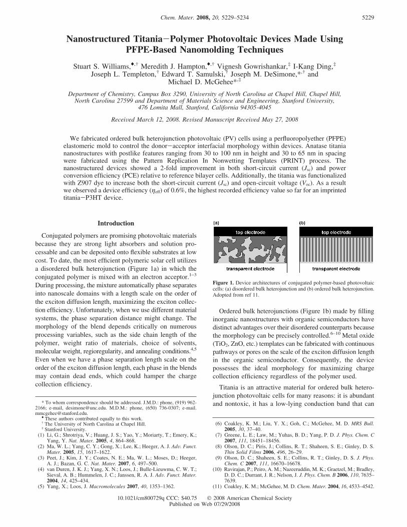
sub-100 nm features. This process, referred to as PRINT
(Pattern Replication In Nonwetting Templates) and shown
in Figure 2, shows great potential for controlling device
architecture in ordered bulk heterojunction solar cells. In this
paper, we present the use of PRINT for patterning anatase
TiO2 on a sub-100 nm length scale. The ordered bulk
heterojunction devices, made by infiltrating titania nano-
structures with poly-3-hexylthiophene (P3HT), show a 2-fold
improvement in short-circuit current relative to flat bilayer
devices.
Results and Discussion
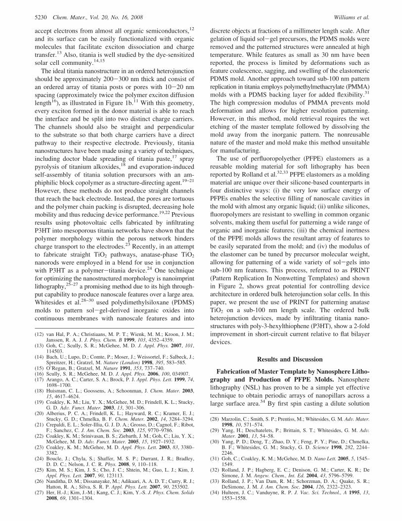
Fabrication of Master Template by Nanosphere Litho-
graphy and Production of PFPE Molds. Nanosphere
lithography (NSL) has proven to be a simple yet effective
technique to obtain periodic arrays of nanopillars across a
large surface area.34 By first spin casting a dilute solution
(12) van Hal, P. A.; Christiaans, M. P. T.; Wienk, M. M.; Kroon, J. M.;Janssen, R. A. J. J. Phys. Chem. B 1999, 103, 4352–4359.
(13) Goh, C.; Scully, S. R.; McGehee, M. D. J. Appl. Phys. 2007, 101,114503.
(14) Bach, U.; Lupo, D.; Comte, P.; Moser, J.; Weissortel, F.; Salbeck, J.;Spreitzer, H.; Gratzel, M. Nature (London) 1998, 395, 583–585.
(15) O’Regan, B.; Gratzel, M. Nature 1991, 353, 737–740.(16) Scully, S. R.; McGehee, M. D. J. Appl. Phys. 2006, 100, 034907.(17) Arango, A. C.; Carter, S. A.; Brock, P. J. Appl. Phys. Lett. 1999, 74,
1698–1700.(18) Huisman, C. L.; Goossens, A.; Schoonman, J. Chem. Mater. 2003,
15, 4617–4624.(19) Coakley, K. M.; Liu, Y. X.; McGehee, M. D.; Frindell, K. L.; Stucky,
G. D. AdV. Funct. Mater. 2003, 13, 301–306.(20) Alberius, P. C. A.; Frindell, K. L.; Hayward, R. C.; Kramer, E. J.;
Stucky, G. D.; Chmelka, B. F. Chem. Mater. 2002, 14, 3284–3294.(21) Crepaldi, E. L.; Soler-Illia, G. J. D. A.; Grosso, D.; Cagnol, F.; Ribot,
F.; Sanchez, C. J. Am. Chem. Soc. 2003, 125, 9770–9786.(22) Coakley, K. M.; Srinivasan, B. S.; Ziebarth, J. M.; Goh, C.; Liu, Y. X.;
McGehee, M. D. AdV. Funct. Mater. 2005, 15, 1927–1932.(23) Coakley, K. M.; McGehee, M. D. Appl. Phys. Lett. 2003, 83, 3380–
3382.(24) Boucle, J.; Chyla, S.; Shaffer, M. S. P.; Durrant, J. R.; Bradley,
D. D. C.; Nelson, J. C. R. Phys. 2008, 9, 110–118.(25) Kim, M. S.; Kim, J. S.; Cho, J. C.; Shtein, M.; Guo, L. J.; Kim, J.
Appl. Phys. Lett. 2007, 90, 123113.(26) Nanditha, D. M.; Dissanayake, M.; Adikaari, A. A. D. T.; Curry, R. J.;
Hatton, R. A.; Silva, S. R. P. Appl. Phys. Lett. 2007, 90, 253502.(27) Her, H.-J.; Kim, J.-M.; Kang, C. J.; Kim, Y.-S. J. Phys. Chem. Solids
2008, 69, 1301–1304.
(28) Marzolin, C.; Smith, S. P.; Prentiss, M.; Whitesides, G. M. AdV. Mater.1998, 10, 571–574.
(29) Yang, H.; Deschatelets, P.; Brittain, S. T.; Whitesides, G. M. AdV.Mater. 2001, 13, 54–58.
(30) Yang, P. D.; Deng, T.; Zhao, D. Y.; Feng, P. Y.; Pine, D.; Chmelka,B. F.; Whitesides, G. M.; Stucky, G. D. Science 1998, 282, 2244–2246.
(31) Goh, C.; Coakley, K. M.; McGehee, M. D. Nano Lett. 2005, 5, 1545–1549.
(32) Rolland, J. P.; Hagberg, E. C.; Denison, G. M.; Carter, K. R.; DeSimone, J. M. Angew. Chem., Int. Ed. 2004, 43, 5796–5799.
(33) Rolland, J. P.; Van Dam, R. M.; Schorzman, D. A.; Quake, S. R.;DeSimone, J. M. J. Am. Chem. Soc. 2004, 126, 2322–2323.
(34) Hulteen, J. C.; Vanduyne, R. P. J. Vac. Sci. Technol., A 1995, 13,1553–1558.
5230 Chem. Mater., Vol. 20, No. 16, 2008 Williams et al.
of polystyrene nanospheres on a silicon wafer, a monolayer
of nanospheres was readily deposited over the entire surface.
These nanospheres are not robust enough to be used directly
as an etch mask for reactive ion etching (RIE); therefore, a
5 nm Cr layer was deposited on top of the nanosphere
monolayer using electron-beam evaporation. The nano-
spheres were then dissolved by sonication in toluene at 60
°C. This process leaves behind islands of Cr that are used
as an etch mask for nanopillars. The height of the final
features in silicon is directly proportional to the time of the
RIE (all other conditions remaining constant). The features
we obtained were randomly oriented postlike structures with
the highest aspect ratio structures having a maximum height
of 140 nm and a diameter of 20 nm. The random orientation
was due to the large variance in nanosphere diameters
(average of 20 nm), which resulted in various sized interstitial
holes between nanospheres where the Cr mask was deposited.
Any Cr remaining on top of the nanopillars was removed
using a standard piranha etch. While the feature shape and
distribution across the wafer varied for each sample, this
method was effective in generating nanoscale patterns across
a large area.
In order to obtain an elastomer mold of the NSL master
template, a liquid PFPE precursor comprised of 1 kDa PFPE
(R,Ω-functionalized dimethacrylate) and 2,2-diethoxyac-
etophenone was poured over the nanopatterned master
template. Due to its very low surface energy, the liquid PFPE
was capable of selectively filling the nanoscale cavities in
the master. Subsequent photochemical cross-linking resulted
in a high-fidelity mold of the nanoscale features of the NSL
master template, as shown in Figure 3.
Feature Replication in Anatase Titania. When fabricat-
ing titania nanostructures for photovoltaic applications, it was
necessary to employ two layers of titania on top of the
fluorine-doped tin oxide (FTO) electrode. The first layer was
a flat, thin film foundation of anatase titania upon which the
nanostructured layer was fabricated. The first thin film of
titania provided a pinhole-free layer that prevents device
shorting as a result of direct pathways between the top and
the bottom electrodes. This was especially important if the
second (patterned) titania layer had any small cracks or
pinholes. Different sol formulations were utilized for the two
layers in order to obtain a crack-free thin film in the first
layer and prevent volume reduction and feature degradation
in the second layer.
In this process, a thin film of sol 1 as the compact
underlayer was deposited onto fluorine-doped tin oxide
(FTO) electrode by spin casting. The samples were then oven
dried and calcined at 450 °C. Subsequently, liquid sol 2 was
drop cast onto the sample and a PFPE mold was pressed
down onto the substrate and held at constant pressure. The
sample was heated to 110 °C to facilitate the sol-gel
transition via solvent removal, a process that was aided by
Figure 2. Illustration of the PRINT process: (a) Si master template; (b) mold release from master template; (c) molding a liquid precursor; (d) patterntransfer to substrate at elevated temperature and pressure; (e) mold release from replica film.
Figure 3. 3 × 3 µm atomic force microscope images of the (a) silicon master fabricated via nanosphere lithography and the (b) 1 kDa PFPE elastomer moldof the master template. z height ) 150 nm for both images.
5231Chem. Mater., Vol. 20, No. 16, 2008Nanostructured Titania-Polymer PhotoVoltaic DeVices
the high permeability of the mold.35 The low-surface energy
PFPE mold was then peeled off the FTO substrate, leaving
an embossed xerogel film. Calcination of the xerogel phase
at 450 °C led to formation of anatase titania features (see
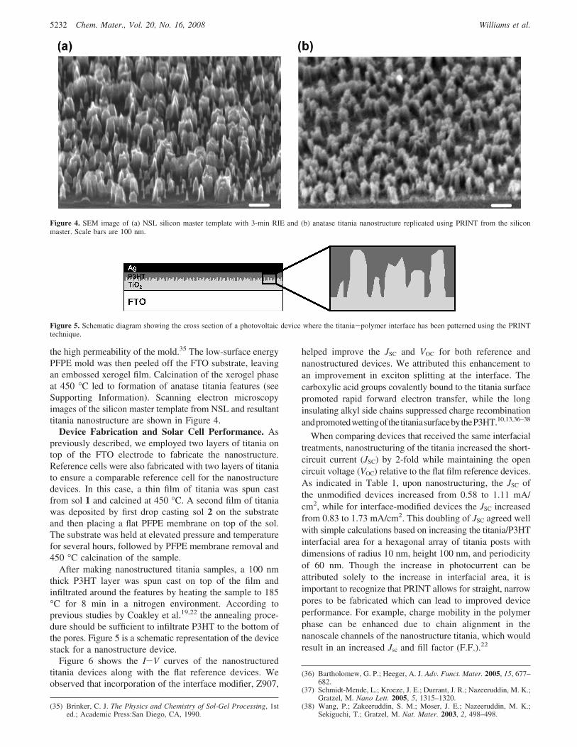
Supporting Information). Scanning electron microscopy
images of the silicon master template from NSL and resultant
titania nanostructure are shown in Figure 4.
Device Fabrication and Solar Cell Performance. As
previously described, we employed two layers of titania on
top of the FTO electrode to fabricate the nanostructure.
Reference cells were also fabricated with two layers of titania
to ensure a comparable reference cell for the nanostructure
devices. In this case, a thin film of titania was spun cast
from sol 1 and calcined at 450 °C. A second film of titania
was deposited by first drop casting sol 2 on the substrate
and then placing a flat PFPE membrane on top of the sol.
The substrate was held at elevated pressure and temperature
for several hours, followed by PFPE membrane removal and
450 °C calcination of the sample.
After making nanostructured titania samples, a 100 nm
thick P3HT layer was spun cast on top of the film and
infiltrated around the features by heating the sample to 185
°C for 8 min in a nitrogen environment. According to
previous studies by Coakley et al.19,22 the annealing proce-
dure should be sufficient to infiltrate P3HT to the bottom of
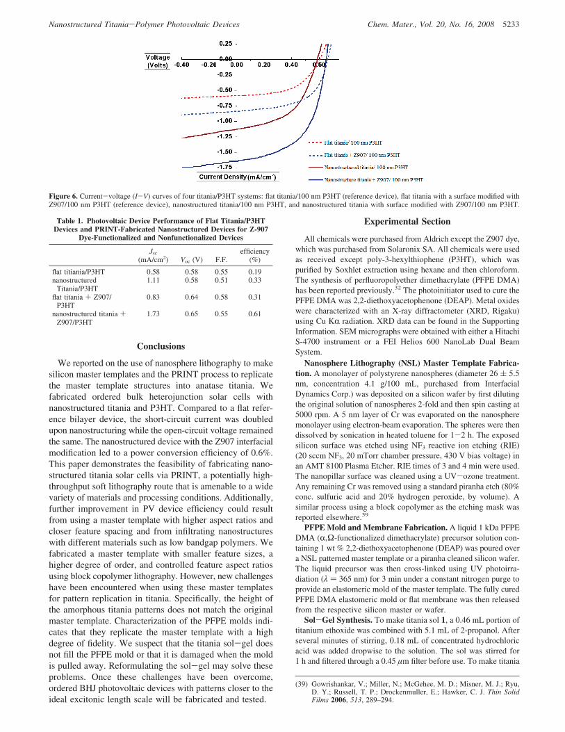
the pores. Figure 5 is a schematic representation of the device
stack for a nanostructure device.
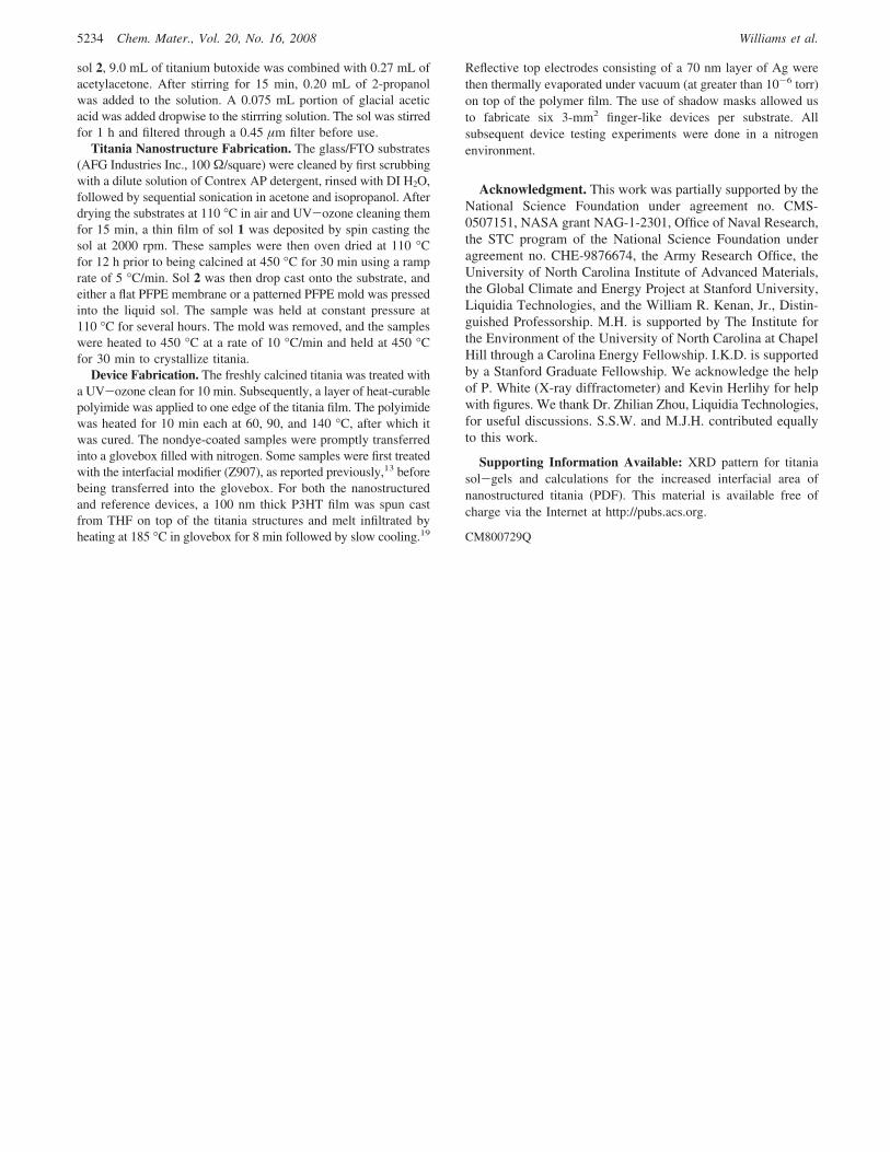
Figure 6 shows the I-V curves of the nanostructured
titania devices along with the flat reference devices. We
observed that incorporation of the interface modifier, Z907,
helped improve the JSC and VOC for both reference and
nanostructured devices. We attributed this enhancement to
an improvement in exciton splitting at the interface. The
carboxylic acid groups covalently bound to the titania surface
promoted rapid forward electron transfer, while the long
insulating alkyl side chains suppressed charge recombination
andpromotedwettingofthetitaniasurfacebytheP3HT.10,13,36–38
When comparing devices that received the same interfacial
treatments, nanostructuring of the titania increased the short-
circuit current (JSC) by 2-fold while maintaining the open
circuit voltage (VOC) relative to the flat film reference devices.
As indicated in Table 1, upon nanostructuring, the JSC of
the unmodified devices increased from 0.58 to 1.11 mA/
cm2, while for interface-modified devices the JSC increased
from 0.83 to 1.73 mA/cm2. This doubling of JSC agreed well
with simple calculations based on increasing the titania/P3HT
interfacial area for a hexagonal array of titania posts with
dimensions of radius 10 nm, height 100 nm, and periodicity
of 60 nm. Though the increase in photocurrent can be
attributed solely to the increase in interfacial area, it is
important to recognize that PRINT allows for straight, narrow
pores to be fabricated which can lead to improved device
performance. For example, charge mobility in the polymer
phase can be enhanced due to chain alignment in the
nanoscale channels of the nanostructure titania, which would
result in an increased Jsc and fill factor (F.F.).22
(35) Brinker, C. J. The Physics and Chemistry of Sol-Gel Processing, 1sted.; Academic Press:San Diego, CA, 1990.
(36) Bartholomew, G. P.; Heeger, A. J. AdV. Funct. Mater. 2005, 15, 677–682.
(37) Schmidt-Mende, L.; Kroeze, J. E.; Durrant, J. R.; Nazeeruddin, M. K.;Gratzel, M. Nano Lett. 2005, 5, 1315–1320.
(38) Wang, P.; Zakeeruddin, S. M.; Moser, J. E.; Nazeeruddin, M. K.;Sekiguchi, T.; Gratzel, M. Nat. Mater. 2003, 2, 498–498.
Figure 4. SEM image of (a) NSL silicon master template with 3-min RIE and (b) anatase titania nanostructure replicated using PRINT from the siliconmaster. Scale bars are 100 nm.
Figure 5. Schematic diagram showing the cross section of a photovoltaic device where the titania-polymer interface has been patterned using the PRINTtechnique.
5232 Chem. Mater., Vol. 20, No. 16, 2008 Williams et al.
Conclusions
We reported on the use of nanosphere lithography to make
silicon master templates and the PRINT process to replicate
the master template structures into anatase titania. We
fabricated ordered bulk heterojunction solar cells with
nanostructured titania and P3HT. Compared to a flat refer-
ence bilayer device, the short-circuit current was doubled
upon nanostructuring while the open-circuit voltage remained
the same. The nanostructured device with the Z907 interfacial
modification led to a power conversion efficiency of 0.6%.
This paper demonstrates the feasibility of fabricating nano-
structured titania solar cells via PRINT, a potentially high-
throughput soft lithography route that is amenable to a wide
variety of materials and processing conditions. Additionally,
further improvement in PV device efficiency could result
from using a master template with higher aspect ratios and
closer feature spacing and from infiltrating nanostructures
with different materials such as low bandgap polymers. We
fabricated a master template with smaller feature sizes, a
higher degree of order, and controlled feature aspect ratios
using block copolymer lithography. However, new challenges
have been encountered when using these master templates
for pattern replication in titania. Specifically, the height of
the amorphous titania patterns does not match the original
master template. Characterization of the PFPE molds indi-
cates that they replicate the master template with a high
degree of fidelity. We suspect that the titania sol-gel does
not fill the PFPE mold or that it is damaged when the mold
is pulled away. Reformulating the sol-gel may solve these
problems. Once these challenges have been overcome,
ordered BHJ photovoltaic devices with patterns closer to the
ideal excitonic length scale will be fabricated and tested.
Experimental Section
All chemicals were purchased from Aldrich except the Z907 dye,
which was purchased from Solaronix SA. All chemicals were used
as received except poly-3-hexylthiophene (P3HT), which was
purified by Soxhlet extraction using hexane and then chloroform.
The synthesis of perfluoropolyether dimethacrylate (PFPE DMA)
has been reported previously.32 The photoinitiator used to cure the
PFPE DMA was 2,2-diethoxyacetophenone (DEAP). Metal oxides
were characterized with an X-ray diffractometer (XRD, Rigaku)
using Cu KR radiation. XRD data can be found in the Supporting
Information. SEM micrographs were obtained with either a Hitachi
S-4700 instrument or a FEI Helios 600 NanoLab Dual Beam
System.
Nanosphere Lithography (NSL) Master Template Fabrica-
tion. A monolayer of polystyrene nanospheres (diameter 26 ( 5.5
nm, concentration 4.1 g/100 mL, purchased from Interfacial
Dynamics Corp.) was deposited on a silicon wafer by first diluting
the original solution of nanospheres 2-fold and then spin casting at
5000 rpm. A 5 nm layer of Cr was evaporated on the nanosphere
monolayer using electron-beam evaporation. The spheres were then
dissolved by sonication in heated toluene for 1-2 h. The exposed
silicon surface was etched using NF3 reactive ion etching (RIE)
(20 sccm NF3, 20 mTorr chamber pressure, 430 V bias voltage) in
an AMT 8100 Plasma Etcher. RIE times of 3 and 4 min were used.
The nanopillar surface was cleaned using a UV-ozone treatment.
Any remaining Cr was removed using a standard piranha etch (80%
conc. sulfuric acid and 20% hydrogen peroxide, by volume). A
similar process using a block copolymer as the etching mask was
reported elsewhere.39
PFPE Mold and Membrane Fabrication. A liquid 1 kDa PFPE
DMA (R,Ω-functionalized dimethacrylate) precursor solution con-
taining 1 wt % 2,2-diethoxyacetophenone (DEAP) was poured over
a NSL patterned master template or a piranha cleaned silicon wafer.
The liquid precursor was then cross-linked using UV photoirra-
diation (λ ) 365 nm) for 3 min under a constant nitrogen purge to
provide an elastomeric mold of the master template. The fully cured
PFPE DMA elastomeric mold or flat membrane was then released
from the respective silicon master or wafer.
Sol-Gel Synthesis. To make titania sol 1, a 0.46 mL portion of
titanium ethoxide was combined with 5.1 mL of 2-propanol. After
several minutes of stirring, 0.18 mL of concentrated hydrochloric
acid was added dropwise to the solution. The sol was stirred for
1 h and filtered through a 0.45 µm filter before use. To make titania
(39) Gowrishankar, V.; Miller, N.; McGehee, M. D.; Misner, M. J.; Ryu,D. Y.; Russell, T. P.; Drockenmuller, E.; Hawker, C. J. Thin SolidFilms 2006, 513, 289–294.
Figure 6. Current-voltage (I-V) curves of four titania/P3HT systems: flat titania/100 nm P3HT (reference device), flat titania with a surface modified withZ907/100 nm P3HT (reference device), nanostructured titania/100 nm P3HT, and nanostructured titania with surface modified with Z907/100 nm P3HT.
Table 1. Photovoltaic Device Performance of Flat Titania/P3HT
Devices and PRINT-Fabricated Nanostructured Devices for Z-907
Dye-Functionalized and Nonfunctionalized Devices
Jsc
(mA/cm2) Voc (V) F.F.efficiency
(%)
flat titiania/P3HT 0.58 0.58 0.55 0.19nanostructured
Titania/P3HT1.11 0.58 0.51 0.33
flat titania + Z907/P3HT
0.83 0.64 0.58 0.31
nanostructured titania +
Z907/P3HT1.73 0.65 0.55 0.61
5233Chem. Mater., Vol. 20, No. 16, 2008Nanostructured Titania-Polymer PhotoVoltaic DeVices
sol 2, 9.0 mL of titanium butoxide was combined with 0.27 mL of
acetylacetone. After stirring for 15 min, 0.20 mL of 2-propanol
was added to the solution. A 0.075 mL portion of glacial acetic
acid was added dropwise to the stirrring solution. The sol was stirred
for 1 h and filtered through a 0.45 µm filter before use.
Titania Nanostructure Fabrication. The glass/FTO substrates
(AFG Industries Inc., 100 Ω/square) were cleaned by first scrubbing
with a dilute solution of Contrex AP detergent, rinsed with DI H2O,
followed by sequential sonication in acetone and isopropanol. After
drying the substrates at 110 °C in air and UV-ozone cleaning them
for 15 min, a thin film of sol 1 was deposited by spin casting the
sol at 2000 rpm. These samples were then oven dried at 110 °C
for 12 h prior to being calcined at 450 °C for 30 min using a ramp
rate of 5 °C/min. Sol 2 was then drop cast onto the substrate, and
either a flat PFPE membrane or a patterned PFPE mold was pressed
into the liquid sol. The sample was held at constant pressure at
110 °C for several hours. The mold was removed, and the samples
were heated to 450 °C at a rate of 10 °C/min and held at 450 °C
for 30 min to crystallize titania.
Device Fabrication. The freshly calcined titania was treated with
a UV-ozone clean for 10 min. Subsequently, a layer of heat-curable
polyimide was applied to one edge of the titania film. The polyimide
was heated for 10 min each at 60, 90, and 140 °C, after which it
was cured. The nondye-coated samples were promptly transferred
into a glovebox filled with nitrogen. Some samples were first treated
with the interfacial modifier (Z907), as reported previously,13 before
being transferred into the glovebox. For both the nanostructured
and reference devices, a 100 nm thick P3HT film was spun cast
from THF on top of the titania structures and melt infiltrated by
heating at 185 °C in glovebox for 8 min followed by slow cooling.19
Reflective top electrodes consisting of a 70 nm layer of Ag were
then thermally evaporated under vacuum (at greater than 10-6 torr)
on top of the polymer film. The use of shadow masks allowed us
to fabricate six 3-mm2 finger-like devices per substrate. All
subsequent device testing experiments were done in a nitrogen
environment.
Acknowledgment. This work was partially supported by the
National Science Foundation under agreement no. CMS-
0507151, NASA grant NAG-1-2301, Office of Naval Research,
the STC program of the National Science Foundation under
agreement no. CHE-9876674, the Army Research Office, the
University of North Carolina Institute of Advanced Materials,
the Global Climate and Energy Project at Stanford University,
Liquidia Technologies, and the William R. Kenan, Jr., Distin-
guished Professorship. M.H. is supported by The Institute for
the Environment of the University of North Carolina at Chapel
Hill through a Carolina Energy Fellowship. I.K.D. is supported
by a Stanford Graduate Fellowship. We acknowledge the help
of P. White (X-ray diffractometer) and Kevin Herlihy for help
with figures. We thank Dr. Zhilian Zhou, Liquidia Technologies,
for useful discussions. S.S.W. and M.J.H. contributed equally
to this work.
Supporting Information Available: XRD pattern for titania
sol-gels and calculations for the increased interfacial area of
nanostructured titania (PDF). This material is available free of
charge via the Internet at http://pubs.acs.org.
CM800729Q
5234 Chem. Mater., Vol. 20, No. 16, 2008 Williams et al.