Embed Size (px)
Citation preview
www.advmat.dewww.MaterialsViews.com
REVIE
W
Hee Han , * Yunseok Kim , Marin Alexe , Dietrich Hesse , and Woo Lee *
Nanostructured Ferroelectrics: Fabrication and Structure–Property Relations
With the continued demand for ultrahigh density ferroelectric data storage applications, it is becoming increasingly important to scale the dimension of ferroelectrics down to the nanometer-scale region and to thoroughly understand the effects of miniaturization on the materials properties. Upon reduction of the physical dimension of the material, the change in physical properties associated with size reduction becomes extremely diffi cult to characterize and to understand because of a complicated interplay between structures, surface properties, strain effects from substrates, domain nuclea-tion, and wall motions. In this Review, the recent progress in fabrication and structure-property relations of nanostructured ferroelectric oxides is sum-marized. Various fabrication approaches are reviewed, with special emphasis on a newly developed stencil-based method for fabricating ferroelectric nanocapacitors, and advantages and limitations of the processes are dis-cussed. Stress-induced evolutions of domain structures upon reduction of the dimension of the material and their implications on the electrical properties are discussed in detail. Distinct domain nucleation, growth, and propaga-tion behaviors in nanometer-scale ferroelectric capacitors are discussed and compared to those of micrometer-scale counterparts. The structural effect of ferroelectric nanocapacitors on the domain switching behavior and cross-talk between neighboring capacitors under external electric fi eld is reviewed.
1. Introduction
Ferroelectricity is a property of materials that means they exhibit spontaneous electric polarization that can be reversed by an external electric fi eld. Ferroelectric materials are required by symmetry considerations to be also piezoelectric and pyroelec-tric. Since the discovery of ferroelectricity in Rochelle salt by
© 2011 WILEY-VCH Verlag GmbH & Co. KGaA, WeinheimAdv. Mater. 2011, 23, 4599–4613
Dr. H. Han , Prof. W. Lee Korea Research Institute of Standards and Science (KRISS)Yuseong, 305-340 Daejeon, Korea E-mail: [email protected]; [email protected] Dr. Y. Kim , [ + ] Dr. M. Alexe , Prof. D. Hesse Max Planck Institute of Microstructure Physics Weinberg 2, 06120 Halle, Germany Prof. W. Lee Department of Nano Science University of Science and Technology (UST)Yuseong, 305-333 Daejeon, Korea [+] Present address: The Center for Nanophase Materials Sciences, Oak Ridge National Laboratory, Oak Ridge, TN 37831, USA
DOI: 10.1002/adma.201102249
Valasek in 1920 [ 1 ] and in BaTiO 3 , [ 2 ] ferroe-lectric complex oxides have been extensively investigated due to their attractive physical properties that can be exploited for many real-life applications. [ 3–9 ] Most applications of ferroelectric oxides are based on the simple capacitor structure, in which a fer-roelectric material is sandwiched between a pair of electrodes. The high dielectric permittivity of ferroelectrics has been utilized to make capacitors with tunable capacitance, the physical sizes of which are much smaller than those of conventional dielectric (non-tunable) capacitors of com-parable capacitance. Pyroelectricity origi-nating from a temperature dependence of the spontaneous polarization has been utilized for ultrasensitive infrared detec-tors. On the other hand, piezoelectricity has made materials applicable to high-performance actuators, vibration sensors, and other devices. Among the many attrac-tive physical properties of ferroelectric oxides, the reversible spontaneous electric polarization has recently attracted much attention, especially in the research fi eld aimed at non-volatile data storage devices.
With ever-increasing demand on portable consumer elec-tronic devices with ultrahigh-density data storage and low power consumption, the miniaturization of ferroelectric capaci-tors has become an important issue. It has been equally impor-tant to understand the effects of size reduction on the ferroelec-tric properties. Upon reduction of the physical dimension of the material, however, understanding the fundamental physics becomes extremely diffi cult because of a complicated interplay between surface properties, strain effects from substrates, and size reduction. To thoroughly understand the basic physics of nanostructured ferroelectrics, size effects originating not only from the thickness of the material, but also from the lateral dimension need to be investigated, i.e., both thickness and the lateral size effects.
Most previous studies on the thickness-related size effect have been dedicated to 2D ultrathin fi lms. This research trend originated from the recent large advances in electrical charac-terization, relevant theories, and deposition techniques. The latter involve, e.g., in situ controlled molecular beam epitaxy (MBE) and pulsed laser deposition (PLD) combined with refl ec-tion high energy electron diffraction (RHEED). [ 10–17 ] It has been experimentally and theoretically explored that periodic domains
4599wileyonlinelibrary.com
4600
www.advmat.dewww.MaterialsViews.com
REVIE
W Hee Han is a postdoc in the group of the Nanomaterials Research Laboratory at the Korea Research Institute of Standards and Science (KRISS). He received his Ph.D. degree from Pohang University of Science and Technology (Department of Materials Science) in 2010. His research focused on the fabrication of ferroelectric nanostructures
and investigation of their size effects. At KRISS, he is working on development of resistive memory capacitors.
Woo Lee is a principal researcher at the Korea Research Institute of Standards and Science (KRISS) and Associate Professor of the Department of Nano Science, University of Science and Technology (UST), Daejeon, Korea. He received his Ph.D. from Seoul National University (2003). From 2003 to 2007, he worked with Prof. Kornelius
Nielsch as a postdoc and then with the late Prof. Ulrich Gösele as a staff researcher at the MPI-Halle. His research interests include anodization electrochemistry of valve metals and growth mechanisms and structure–property relationships of low-dimensional materials, as well as their applications to memory and energy-harvesting devices.
with opposite polarization direction and conducting electrodes can stabilize ferroelectricity, even in ferroelectric fi lms with a thickness of three and six perovskite unit cells, which indi-cates that a fundamental limit on the thickness of ferroelectric thin fi lms has been overcome or may not exist. [ 12 , 17 ] However, only a few studies focusing on the lateral size effect have been reported because of the diffi culties not only in fabricating struc-turally well-defi ned ferroelectric nanostructures, but also in characterizing the physical properties on the nanometer length scale. [ 18–22 ]
This article gives an overview on recent advances in nano-structured ferroelectric complex oxides, focusing on the fabrica-tion and the structure–property relationships of nanocapacitors and nanoislands. Various approaches that have been employed so far for the fabrication of ferroelectric nanostructures are reviewed and the advantages and limitations of the respective processes are discussed. A promising approach for the realiza-tion of extended arrays of ferroelectric nanocapacitors is pre-sented. The strain-induced evolution of domain structures in 2D continuous ferroelectric thin fi lms and 0D discrete ferroelectric nanodots and its implications for the electrical properties, such as piezoresponse, are discussed. Individual data addressability, retention, and switching uniformity of extended arrays of fer-roelectric nanocapacitors are presented. Domain switching in nanometer-scale ferroelectric capacitors was observed to be dif-ferent from that of micrometer-scale counterparts. A recently proposed phenomenological model that may explain domain nucleation, growth, and propagation in ferroelectric nanocapac-itors is presented. The discussion also covers cross-talk between neighboring nanocapacitors under external bias, which should be systematically investigated for a successful development of reliable non-volatile data storage devices.
2. Fabrication of Ferroelectric Nanostructures
The electrical properties of nanostructured ferroelectric oxides are very sensitive to the compositional homogeneity, the crystal-line quality, and the physical dimension of materials. [ 18–25 ] For thorough understanding of the intrinsic properties of nanostruc-tured ferroelectrics, one should be able to control the shape and size of the materials at will, engineer the lattice strain at the interface of a ferroelectric oxide and the underlying sub-strate, and arrange materials on a substrate of considerably large size for practical applications of ferroelectrics to ultrahigh density non-volatile memories. Correspondingly, the fabrication approach should meet the following basic requirements: i) the method itself needs to be cheap and easily accessible, allowing for an easy control of the size and shape in the sub-one-hundred nanometer region as well as mass production of desired struc-tures with a narrow size distribution and ii) the approach is required to be high-temperature compatible. To date, various approaches have been employed for the fabrication of structur-ally well-defi ned ferroelectric nanostructures. [ 26–60 ] The fabrica-tion strategies so far can be classifi ed into two broad groups: top-down and bottom-up approaches. In the following sections, we give an overview on some of the recent advances in the fab-rication of nanostructured ferroelectric oxides. We discuss the advantages and limitations of the conventional top-down and
© 2011 WILEY-VCH Verlag Gwileyonlinelibrary.com
bottom-up approaches. Some attempts to resolve the issues in conventional nanofabrication processes will also be discussed, focusing on our recent approach to realize extended 2D arrays of ferroelectric nanocapacitors by properly combining the var-ious merits of conventional processes. Various approaches for fabrication of nanostructured ferroelectrics of nanocapacitor and nanoisland types are summarized in Table 1 .
2.1. Top-Down Approaches
Top-down approaches are based on the reduction of feature size through etching or removal of material from a large struc-ture. The approach mainly relies on lithography processes by utilizing energetic particles such as photons, ions, or electron beams. It includes focused ion beam (FIB) milling and electron beam (EB) direct writing (EBDW) of a metalorganic precursor fi lm followed by high-temperature annealing for crystallization as shown in Figure 1 . [ 26–33 ]
The FIB technique is one of the most popular methods for fabricating ferroelectric nanocapacitors with controlled feature
mbH & Co. KGaA, Weinheim Adv. Mater. 2011, 23, 4599–4613
www.advmat.dewww.MaterialsViews.com
REVIE
W
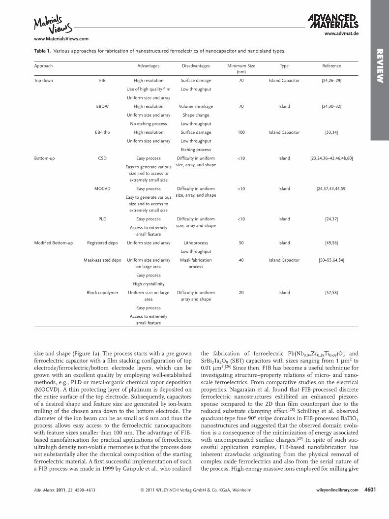
Table 1. Various approaches for fabrication of nanostructured ferroelectrics of nanocapacitor and nanoisland types.
Approach Advantages Disadvantages Minimum Size (nm)
Type Reference
Top-down FIB High resolution Surface damage 70 Island Capacitor [24,26–29]
Use of high quality fi lm Low throughput
Uniform size and array
EBDW High resolution Volume shrinkage 70 Island [24,30–32]
Uniform size and array Shape change
No etching process Low throughput
EB-litho High resolution Surface damage 100 Island Capacitor [33,34]
Uniform size and array Low throughput
Etching process
Bottom-up CSD Easy process Diffi culty in uniform
size, array, and shape < 10 Island [23,24,36–42,46,48,60]
Easy to generate various
size and to access to
extremely small size
MOCVD Easy process Diffi culty in uniform
size, array, and shape < 10 Island [24,37,43,44,59]
Easy to generate various
size and to access to
extremely small size
PLD Easy process Diffi culty in uniform
size, array and shape < 10 Island [24,37]
Access to extremely
small feature
Modifi ed Bottom-up Registered depo Uniform size and array Lithoprocess 50 Island [49,56]
Low throughput
Mask-assisted depo Uniform size and array
on large area
Mask fabrication
process
40 Island Capacitor [50–55,64,84]
Easy process
High crystallinity
Block copolymer Uniform size on large
area
Diffi culty in uniform
array and shape
20 Island [57,58]
Easy process
Access to extremely
small feature
size and shape (Figure 1 a). The process starts with a pre-grown ferroelectric capacitor with a fi lm stacking confi guration of top electrode/ferroelectric/bottom electrode layers, which can be grown with an excellent quality by employing well-established methods, e.g., PLD or metal-organic chemical vapor deposition (MOCVD). A thin protecting layer of platinum is deposited on the entire surface of the top electrode. Subsequently, capacitors of a desired shape and feature size are generated by ion-beam milling of the chosen area down to the bottom electrode. The diameter of the ion beam can be as small as 6 nm and thus the process allows easy access to the ferroelectric nanocapacitors with feature sizes smaller than 100 nm. The advantage of FIB-based nanofabrication for practical applications of ferroelectric ultrahigh density non-volatile memories is that the process does not substantially alter the chemical composition of the starting ferroelectric material. A fi rst successful implementation of such a FIB process was made in 1999 by Ganpule et al., who realized
© 2011 WILEY-VCH Verlag GAdv. Mater. 2011, 23, 4599–4613
the fabrication of ferroelectric Pb(Nb 0.04 Zr 0.28 Ti 0.68 )O 3 and SrBi 2 Ta 2 O 9 (SBT) capacitors with sizes ranging from 1 μ m 2 to 0.01 μ m 2 . [ 26 ] Since then, FIB has become a useful technique for investigating structure–property relations of micro- and nano-scale ferroelectrics. From comparative studies on the electrical properties, Nagarajan et al. found that FIB-processed discrete ferroelectric nanostructures exhibited an enhanced piezore-sponse compared to the 2D thin fi lm counterpart due to the reduced substrate clamping effect. [ 28 ] Schilling et al. observed quadrant-type fi ne 90 ° stripe domains in FIB-processed BaTiO 3 nanostructures and suggested that the observed domain evolu-tion is a consequence of the minimization of energy associated with uncompensated surface charges. [ 29 ] In spite of such suc-cessful application examples, FIB-based nanofabrication has inherent drawbacks originating from the physical removal of complex oxide ferroelectrics and also from the serial nature of the process. High-energy massive ions employed for milling give
4601mbH & Co. KGaA, Weinheim wileyonlinelibrary.com
46
www.advmat.dewww.MaterialsViews.com
REVIE
W
Figure 1 . Two typical examples of top-down approach for nanostructured ferroelectrics: a) focused ion-beam (FIB) milling and b) EB direct writing (EBDW). Schematics of the respective nanofabrication processes (upper panel) and representative scanning electron microscopy (SEM) images of the resulting nanostructures (lower panel). Reproduced with permis-sion. [ 26 , 30 ] Copyright 1999, American Institute of Physics.
i) development
ii) crystallization
ion milling
electron beam
metalorganic
precursor
(a) (b)
Pt -protecting
layer
substrate
ferroelectricferroelectric
bottom
electrodeferroelectric
film
top electrode
nanoislands
rise to damage of the oxide lattice at the etched surfaces, which is the major cause of serious deterioration of electrical proper-ties. The side surfaces of FIB-generated ferroelectric nanostruc-tures are often contaminated with undesired materials due to redeposition of the etch products and due to an implantation of the beam material, e.g., gallium, which becomes serious as the feature size of the ferroelectrics decreases.
The EBDW technique is another useful mask-less top-down method and has widely been employed for generating metallic or oxide nanostructures (Figure 1 b). The process starts with a metal-organic precursor thin fi lm. Chemical reactions are locally induced in the metal-organic thin fi lm by irradiation with an EB that has suffi cient energy and dose, and the desired patterns are impressed by scanning the EB over the sample sur-face. The patterns are developed by dissolving the unexposed area in a specifi c solvent. Subsequently, the resulting metal-organic mesas are transformed into ferroelectric oxide by high-temperature annealing, during which a change in the original shape of the mesas takes place due to densifi cation or volume shrinkage. [ 30 ] Alexe et al. demonstrated the fabrication of peri-odic patterns of ferroelectric SBT and Pb(Zr 0.7 Ti 0.3 )O 3 (PZT) with a pattern density of ca. 1 Gbit cm − 2 . [ 30 ] The generated fer-roelectric nanostructures were polycrystalline with grains of 20 nm diameter or less. From piezoresponse force microscopy (PFM) investigations, they found that the fabricated ferroelectric nanoislands exhibit negative vertical shifts of the piezoelectric hysteresis loops, which was attributed to the pinned domains
02 © 2011 WILEY-VCH Verlag Gwileyonlinelibrary.com
both at the free surface and at the ferroelectric/electrode inter-face. [ 31 ] The thicknesses of the pinned layers were estimated to be ca. 35 nm for the free surface and 10 nm for the ferroelec-tric/electrode interface. These results imply that for practical applications polycrystalline ferroelectric nanoislands need to be larger than 70 nm. Using conventional EB lithography, Bühlmann et al. fabricated PZT nanoislands with different feature sizes and found that ferroelectric nanoislands with fea-ture sizes below 300 nm exhibit very high piezoresponse. [ 33 ] The observed enhancement in the electrical properties was attributed to the vanishing of a -domains in nanometer-scale ferroelectrics. The origin of such enhancement needs to be further explored by systematic investigations on the evolution of the domain structure as a function of dimensions of ferro-electric oxides in the nanometer length region.
As discussed above, top-down approaches provide a good opportunity for resolving the issues of precise positioning and tight control of the shape and size of nanostructured ferro-electrics, enabling to some extent investigations of structure–property relationships. However, enormous challenges remain to be overcome due to drawbacks originating from the serial nature of conventional top-down processes, in particular the time-consuming and low-throughput character of these processes.
2.2. Bottom-Up Approaches
Bottom-up approaches are based on naturally occurring self-assembly of atoms, molecules, or nanoparticles for the reali-zation of ferroelectric nanostructures. The approach provides several distinct advantages over top-down based nanofabrica-tions. It allows one to easily access the critical size of fer-roelectric materials, below which ferroelectricity vanishes completely, i.e., the superparaelectric limit. In addition, the processed ferroelectric nanostructures are single crystal-line and free from lattice defects near the surface. However, bottom-up based nanofabrications have limitations in terms of control of size and shape as well as precise positioning of nanoscale ferroelectrics because they rely on either ther-modynamically driven reorganization or self-assembly processes.
Typical bottom-up approaches for ferroelectric nanostruc-tures include chemical solution deposition (CSD) ( Figure 2 a) and MOCVD (Figure 2 b). They utilize the microstructural instability of thin precursor fi lms at high temperatures driven by the tendency to minimize their interface energy between the fi lm and the underlying substrate when the fi lm thickness is below a certain threshold. [ 36–42 , 45 , 46 , 60 ] The initial fi lm thick-ness, the annealing temperature, and the crystallographic orientations of the substrate are known to determine both the size and shape of the resulting ferroelectric nanostruc-tures. [ 38 , 44 ] In general, ferroelectric nanograins with relatively uniform size and shape can be obtained from ultrathin pre-cursor fi lms by high-temperature annealing for an extended period of time.
Roelofs et al. reported that CSD-grown PbTiO 3 (PTO) nanograins undergo a phase transition from ferroelectric to superparaelectric, losing their ferroelectricity, when their lateral
mbH & Co. KGaA, Weinheim Adv. Mater. 2011, 23, 4599–4613
www.advmat.dewww.MaterialsViews.com
REVIE
W
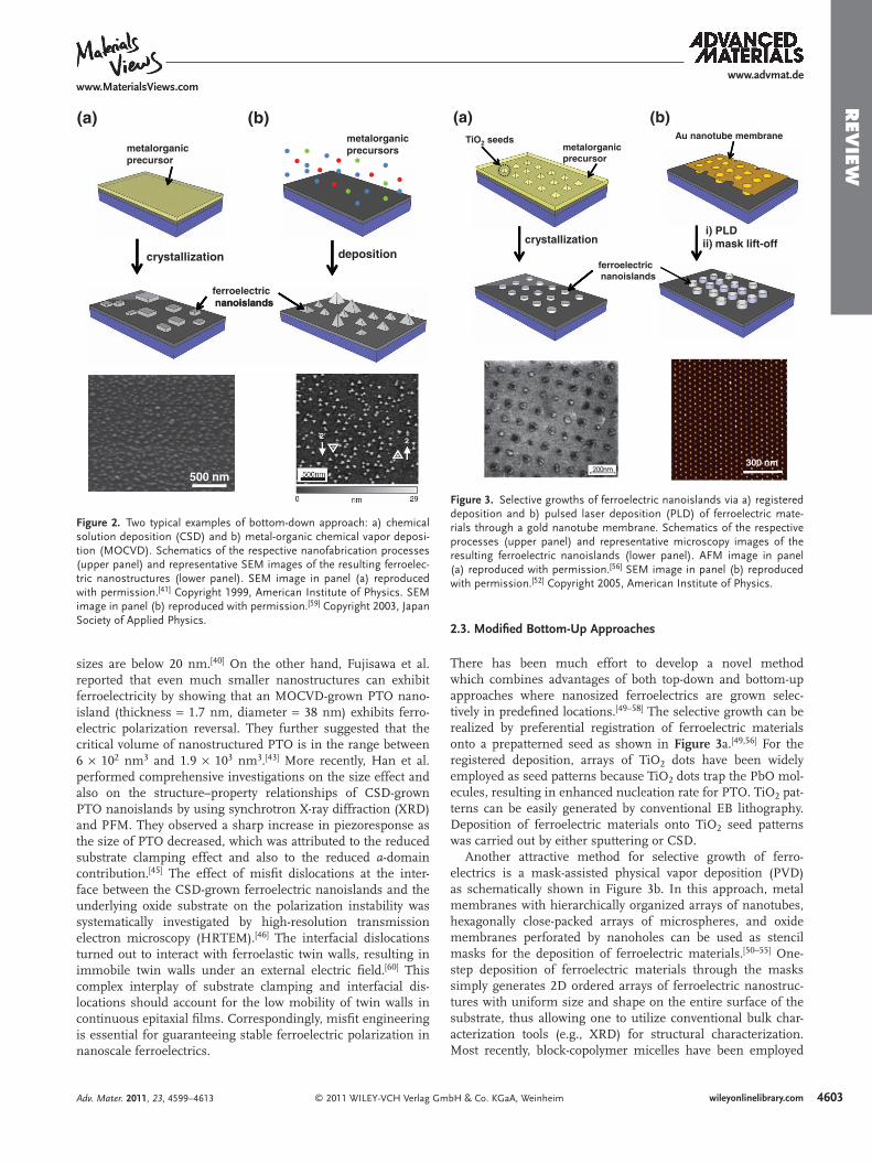
Figure 2 . Two typical examples of bottom-down approach: a) chemical solution deposition (CSD) and b) metal-organic chemical vapor deposi-tion (MOCVD). Schematics of the respective nanofabrication processes (upper panel) and representative SEM images of the resulting ferroelec-tric nanostructures (lower panel). SEM image in panel (a) reproduced with permission. [ 41 ] Copyright 1999, American Institute of Physics. SEM image in panel (b) reproduced with permission. [ 59 ] Copyright 2003, Japan Society of Applied Physics.
crystallization deposition
metalorganic
precursor
metalorganic
precursors
(a) (b)
ferroelectric
nanoislands
500 nm
nanoislands
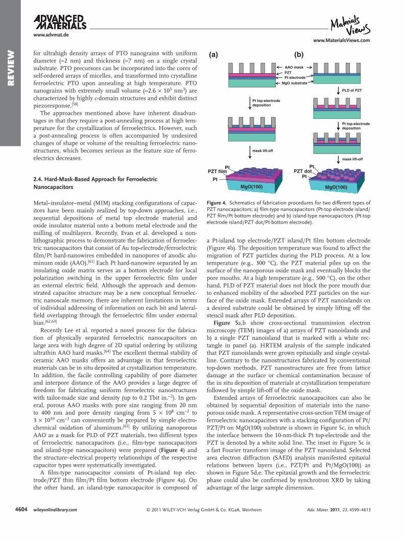
Figure 3 . Selective growths of ferroelectric nanoislands via a) registered deposition and b) pulsed laser deposition (PLD) of ferroelectric mate-rials through a gold nanotube membrane. Schematics of the respective processes (upper panel) and representative microscopy images of the resulting ferroelectric nanoislands (lower panel). AFM image in panel (a) reproduced with permission. [ 56 ] SEM image in panel (b) reproduced with permission. [ 52 ] Copyright 2005, American Institute of Physics.
i) PLD
ii) mask lift-off
Au nanotube membrane
)b()a(
crystallization
metalorganic
precursor
TiO2 seeds
ferroelectric
nanoislands
300 nm
sizes are below 20 nm. [ 40 ] On the other hand, Fujisawa et al. reported that even much smaller nanostructures can exhibit ferroelectricity by showing that an MOCVD-grown PTO nano-island (thickness = 1.7 nm, diameter = 38 nm) exhibits ferro-electric polarization reversal. They further suggested that the critical volume of nanostructured PTO is in the range between 6 × 10 2 nm 3 and 1.9 × 10 3 nm 3 . [ 43 ] More recently, Han et al. performed comprehensive investigations on the size effect and also on the structure–property relationships of CSD-grown PTO nanoislands by using synchrotron X-ray diffraction (XRD) and PFM. They observed a sharp increase in piezoresponse as the size of PTO decreased, which was attributed to the reduced substrate clamping effect and also to the reduced a -domain contribution. [ 45 ] The effect of misfi t dislocations at the inter-face between the CSD-grown ferroelectric nanoislands and the underlying oxide substrate on the polarization instability was systematically investigated by high-resolution transmission electron microscopy (HRTEM). [ 46 ] The interfacial dislocations turned out to interact with ferroelastic twin walls, resulting in immobile twin walls under an external electric fi eld. [ 60 ] This complex interplay of substrate clamping and interfacial dis-locations should account for the low mobility of twin walls in continuous epitaxial fi lms. Correspondingly, misfi t engineering is essential for guaranteeing stable ferroelectric polarization in nanoscale ferroelectrics.
© 2011 WILEY-VCH Verlag GmAdv. Mater. 2011, 23, 4599–4613
2.3. Modifi ed Bottom-Up Approaches
There has been much effort to develop a novel method which combines advantages of both top-down and bottom-up approaches where nanosized ferroelectrics are grown selec-tively in predefi ned locations. [ 49–58 ] The selective growth can be realized by preferential registration of ferroelectric materials onto a prepatterned seed as shown in Figure 3 a. [ 49 , 56 ] For the registered deposition, arrays of TiO 2 dots have been widely employed as seed patterns because TiO 2 dots trap the PbO mol-ecules, resulting in enhanced nucleation rate for PTO. TiO 2 pat-terns can be easily generated by conventional EB lithography. Deposition of ferroelectric materials onto TiO 2 seed patterns was carried out by either sputtering or CSD.
Another attractive method for selective growth of ferro-electrics is a mask-assisted physical vapor deposition (PVD) as schematically shown in Figure 3 b. In this approach, metal membranes with hierarchically organized arrays of nanotubes, hexagonally close-packed arrays of microspheres, and oxide membranes perforated by nanoholes can be used as stencil masks for the deposition of ferroelectric materials. [ 50–55 ] One-step deposition of ferroelectric materials through the masks simply generates 2D ordered arrays of ferroelectric nanostruc-tures with uniform size and shape on the entire surface of the substrate, thus allowing one to utilize conventional bulk char-acterization tools (e.g., XRD) for structural characterization. Most recently, block-copolymer micelles have been employed
4603bH & Co. KGaA, Weinheim wileyonlinelibrary.com
4604
www.advmat.dewww.MaterialsViews.com
REVIE
W
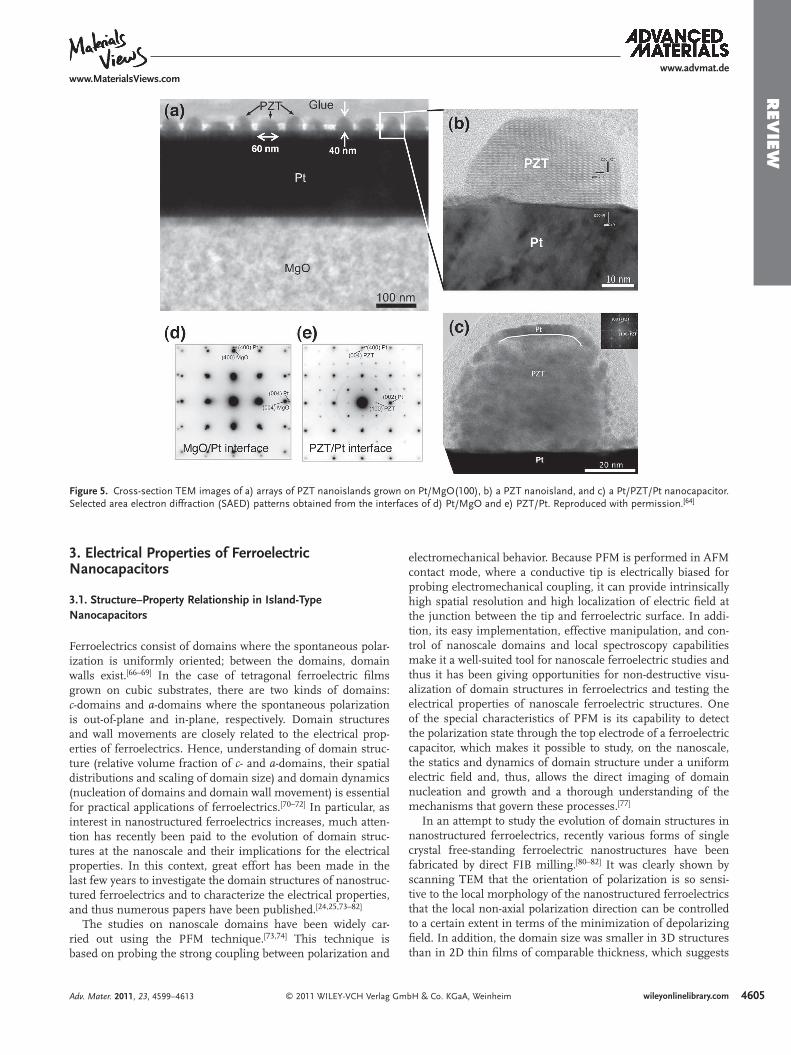
Figure 4 . Schematics of fabrication procedures for two different types of PZT nanocapacitors: a) fi lm-type nanocapacitors (Pt-top electrode island/PZT fi lm/Pt bottom electrode) and b) island-type nanocapacitors (Pt-top electrode island/PZT dot/Pt-bottom electrode).
)b()a(
Pt top-electrode
deposition
PLD of PZT
Pt top-electrode
AAO mask
PZT
Pt electrode
MgO substrate
PZT filmPt
Pt
MgO(100) MgO(100)
PZT dotPt
Pt
mask lift-off
Pt top electrode
deposition
mask lift-off
for ultrahigh density arrays of PTO nanograins with uniform diameter ( ≈ 2 nm) and thickness ( ≈ 7 nm) on a single crystal substrate. PTO precursors can be incorporated into the cores of self-ordered arrays of micelles, and transformed into crystalline ferroelectric PTO upon annealing at high temperature. PTO nanograins with extremely small volume ( ≈ 2.6 × 10 3 nm 3 ) are characterized by highly c -domain structures and exhibit distinct piezoresponse. [ 58 ]
The approaches mentioned above have inherent disadvan-tages in that they require a post-annealing process at high tem-perature for the crystallization of ferroelectrics. However, such a post-annealing process is often accompanied by undesired changes of shape or volume of the resulting ferroelectric nano-structures, which becomes serious as the feature size of ferro-electrics decreases.
2.4. Hard-Mask-Based Approach for Ferroelectric Nanocapacitors
Metal–insulator–metal (MIM) stacking confi gurations of capac-itors have been mainly realized by top-down approaches, i.e., sequential depositions of metal top electrode material and oxide insulator material onto a bottom metal electrode and the milling of multilayers. Recently, Evan et al. developed a non-lithographic process to demonstrate the fabrication of ferroelec-tric nanocapacitors that consist of Au top-electrode/ferroelectric fi lm/Pt hard-nanowires embedded in nanopores of anodic alu-minum oxide (AAO). [ 61 ] Each Pt hard-nanowire separated by an insulating oxide matrix serves as a bottom electrode for local polarization switching in the upper ferroelectric fi lm under an external electric fi eld. Although the approach and demon-strated capacitor structure may be a new conceptual ferroelec-tric nanoscale memory, there are inherent limitations in terms of individual addressing of information on each bit and lateral-fi eld overlapping through the ferroelectric fi lm under external bias. [ 62 , 63 ]
Recently Lee et al. reported a novel process for the fabrica-tion of physically separated ferroelectric nanocapacitors on large area with high degree of 2D spatial ordering by utilizing ultrathin AAO hard masks. [ 64 ] The excellent thermal stability of ceramic AAO masks offers an advantage in that ferroelectric materials can be in situ deposited at crystallization temperature. In addition, the facile controlling capability of pore dia meter and interpore distance of the AAO provides a large degree of freedom for fabricating uniform ferroelectric nanostructures with tailor-made size and density (up to 0.2 Tbit in. − 2 ). In gen-eral, porous AAO masks with pore size ranging from 20 nm to 400 nm and pore density ranging from 5 × 10 8 cm − 2 to 3 × 10 10 cm − 2 can conveniently be prepared by simple electro-chemical oxidation of aluminum. [ 65 ] By utilizing nanoporous AAO as a mask for PLD of PZT materials, two different types of ferroelectric nanocapacitors (i.e., fi lm-type nanocapacitors and island-type nanocapacitors) were prepared ( Figure 4 ) and the structure–electrical property relationships of the respective capacitor types were systematically investigated.
A fi lm-type nanocapacitor consists of Pt-island top elec-trode/PZT thin fi lm/Pt fi lm bottom electrode (Figure 4 a). On the other hand, an island-type nanocapacitor is composed of
© 2011 WILEY-VCH Verlag Gwileyonlinelibrary.com
a Pt-island top electrode/PZT island/Pt fi lm bottom electrode (Figure 4 b). The deposition temperature was found to affect the migration of PZT particles during the PLD process. At a low temperature (e.g., 300 ° C), the PZT material piles up on the surface of the nanoporous oxide mask and eventually blocks the pore mouths. At a high temperature (e.g., 500 ° C), on the other hand, PLD of PZT material does not block the pore mouth due to enhanced mobility of the adsorbed PZT particles on the sur-face of the oxide mask. Extended arrays of PZT nanoislands on a desired substrate could be obtained by simply lifting off the stencil mask after PLD deposition.
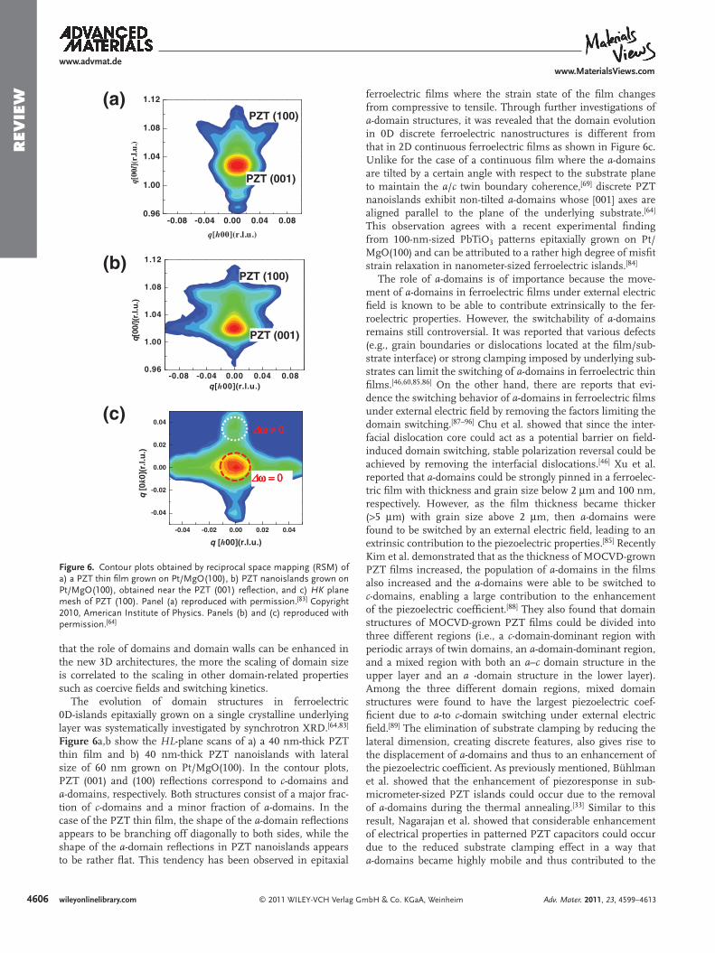
Figure 5 a,b show cross-sectional transmission electron microscopy (TEM) images of a) arrays of PZT nanoislands and b) a single PZT nanoisland that is marked with a white rec-tangle in panel (a). HRTEM analysis of the sample indicated that PZT nanoislands were grown epitaxially and single crystal-line. Contrary to the nanostructures fabricated by conventional top-down methods, PZT nanostructures are free from lattice damage at the surface or chemical contamination because of the in situ deposition of materials at crystallization temperature followed by simple lift-off of the oxide mask.
Extended arrays of ferroelectric nanocapacitors can also be obtained by sequential deposition of materials into the nano-porous oxide mask. A representative cross-section TEM image of ferroelectric nanocapacitors with a stacking confi guration of Pt/PZT/Pt on MgO(100) substrate is shown in Figure 5 c, in which the interface between the 10-nm-thick Pt top-electrode and the PZT is denoted by a white solid line. The inset in Figure 5 c is a fast Fourier transform image of the PZT nanoisland. Selected area electron diffraction (SAED) analysis manifested epitaxial relations between layers (i.e., PZT/Pt and Pt/MgO(100)) as shown in Figure 5 d,e. The epitaxial growth and the ferroelectric phase could also be confi rmed by synchrotron XRD by taking advantage of the large sample dimension.
mbH & Co. KGaA, Weinheim Adv. Mater. 2011, 23, 4599–4613
www.advmat.dewww.MaterialsViews.com
REVIE
W
Figure 5 . Cross-section TEM images of a) arrays of PZT nanoislands grown on Pt/MgO(100), b) a PZT nanoisland, and c) a Pt/PZT/Pt nanocapacitor. Selected area electron diffraction (SAED) patterns obtained from the interfaces of d) Pt/MgO and e) PZT/Pt. Reproduced with permission. [ 64 ]
3. Electrical Properties of Ferroelectric Nanocapacitors
3.1. Structure–Property Relationship in Island-Type Nanocapacitors
Ferroelectrics consist of domains where the spontaneous polar-ization is uniformly oriented; between the domains, domain walls exist. [ 66–69 ] In the case of tetragonal ferroelectric fi lms grown on cubic substrates, there are two kinds of domains: c -domains and a -domains where the spontaneous polarization is out-of-plane and in-plane, respectively. Domain structures and wall movements are closely related to the electrical prop-erties of ferroelectrics. Hence, understanding of domain struc-ture (relative volume fraction of c - and a -domains, their spatial distributions and scaling of domain size) and domain dynamics (nucleation of domains and domain wall movement) is essential for practical applications of ferroelectrics. [ 70–72 ] In particular, as interest in nanostructured ferroelectrics increases, much atten-tion has recently been paid to the evolution of domain struc-tures at the nanoscale and their implications for the electrical properties. In this context, great effort has been made in the last few years to investigate the domain structures of nanostruc-tured ferroelectrics and to characterize the electrical properties, and thus numerous papers have been published. [ 24 , 25 , 73–82 ]
The studies on nanoscale domains have been widely car-ried out using the PFM technique. [ 73 , 74 ] This technique is based on probing the strong coupling between polarization and
© 2011 WILEY-VCH Verlag GmAdv. Mater. 2011, 23, 4599–4613
electromechanical behavior. Because PFM is performed in AFM contact mode, where a conductive tip is electrically biased for probing electromechanical coupling, it can provide intrinsically high spatial resolution and high localization of electric fi eld at the junction between the tip and ferroelectric surface. In addi-tion, its easy implementation, effective manipulation, and con-trol of nanoscale domains and local spectroscopy capabilities make it a well-suited tool for nanoscale ferroelectric studies and thus it has been giving opportunities for non-destructive visu-alization of domain structures in ferroelectrics and testing the electrical properties of nanoscale ferroelectric structures. One of the special characteristics of PFM is its capability to detect the polarization state through the top electrode of a ferroelectric capacitor, which makes it possible to study, on the nanoscale, the statics and dynamics of domain structure under a uniform electric fi eld and, thus, allows the direct imaging of domain nucleation and growth and a thorough understanding of the mechanisms that govern these processes. [ 77 ]
In an attempt to study the evolution of domain structures in nanostructured ferroelectrics, recently various forms of single crystal free-standing ferroelectric nanostructures have been fabricated by direct FIB milling. [ 80–82 ] It was clearly shown by scanning TEM that the orientation of polarization is so sensi-tive to the local morphology of the nanostructured ferroelectrics that the local non-axial polarization direction can be controlled to a certain extent in terms of the minimization of depolarizing fi eld. In addition, the domain size was smaller in 3D structures than in 2D thin fi lms of comparable thickness, which suggests
4605bH & Co. KGaA, Weinheim wileyonlinelibrary.com
460
www.advmat.dewww.MaterialsViews.com
REVIE
W
Figure 6 . Contour plots obtained by reciprocal space mapping (RSM) of a) a PZT thin fi lm grown on Pt/MgO(100), b) PZT nanoislands grown on Pt/MgO(100), obtained near the PZT (001) refl ection, and c) HK plane mesh of PZT (100). Panel (a) reproduced with permission. [ 83 ] Copyright 2010, American Institute of Physics. Panels (b) and (c) reproduced with permission. [ 64 ]
1.04
1.08
1.12
](r.
l.u
.)
PZT (100)
(a)
-0.08 -0.04 0.00 0.04 0.080.96
1.00
1.04
1.08
1.12
q[h00](r.l.u.)
q[00l](r.l.u.)
PZT (100)
PZT (001)
(b)
-0.08 -0.04 0.00 0.04 0.080.96
1.00
q[h00](r.l.u.)
q[00l]
PZT (001)
-0.04 -0.02 0.00 0.02 0.04
-0.04
-0.02
0.00
0.02
0.04
q [h00](r.l.u.)
q [
0k0
](r.
l.u
.)
ΔΔΔΔω ω ωω ≠≠≠≠ 0000
ΔΔΔΔω ω ωω = 00 = 0 == 0
(c)
that the role of domains and domain walls can be enhanced in the new 3D architectures, the more the scaling of domain size is correlated to the scaling in other domain-related properties such as coercive fi elds and switching kinetics.
The evolution of domain structures in ferroelectric 0D-islands epitaxially grown on a single crystalline underlying layer was systematically investigated by synchrotron XRD. [ 64 , 83 ] Figure 6 a,b show the HL -plane scans of a) a 40 nm-thick PZT thin fi lm and b) 40 nm-thick PZT nanoislands with lateral size of 60 nm grown on Pt/MgO(100). In the contour plots, PZT (001) and (100) refl ections correspond to c -domains and a -domains, respectively. Both structures consist of a major frac-tion of c -domains and a minor fraction of a -domains. In the case of the PZT thin fi lm, the shape of the a -domain refl ections appears to be branching off diagonally to both sides, while the shape of the a -domain refl ections in PZT nanoislands appears to be rather fl at. This tendency has been observed in epitaxial
6 © 2011 WILEY-VCH Verlag Gwileyonlinelibrary.com
ferroelectric fi lms where the strain state of the fi lm changes from compressive to tensile. Through further investigations of a -domain structures, it was revealed that the domain evolution in 0D discrete ferroelectric nanostructures is different from that in 2D continuous ferroelectric fi lms as shown in Figure 6 c. Unlike for the case of a continuous fi lm where the a -domains are tilted by a certain angle with respect to the substrate plane to maintain the a / c twin boundary coherence, [ 69 ] discrete PZT nanoislands exhibit non-tilted a -domains whose [001] axes are aligned parallel to the plane of the underlying substrate. [ 64 ] This observation agrees with a recent experimental fi nding from 100-nm-sized PbTiO 3 patterns epitaxially grown on Pt/MgO(100) and can be attributed to a rather high degree of misfi t strain relaxation in nanometer-sized ferroelectric islands. [ 84 ]
The role of a -domains is of importance because the move-ment of a -domains in ferroelectric fi lms under external electric fi eld is known to be able to contribute extrinsically to the fer-roelectric properties. However, the switchability of a -domains remains still controversial. It was reported that various defects (e.g., grain boundaries or dislocations located at the fi lm/sub-strate interface) or strong clamping imposed by underlying sub-strates can limit the switching of a -domains in ferroelectric thin fi lms. [ 46 , 60 , 85 , 86 ] On the other hand, there are reports that evi-dence the switching behavior of a -domains in ferroelectric fi lms under external electric fi eld by removing the factors limiting the domain switching. [ 87–96 ] Chu et al. showed that since the inter-facial dislocation core could act as a potential barrier on fi eld-induced domain switching, stable polarization reversal could be achieved by removing the interfacial dislocations. [ 46 ] Xu et al. reported that a -domains could be strongly pinned in a ferroelec-tric fi lm with thickness and grain size below 2 μ m and 100 nm, respectively. However, as the fi lm thickness became thicker ( > 5 μ m) with grain size above 2 μ m, then a -domains were found to be switched by an external electric fi eld, leading to an extrinsic contribution to the piezoelectric properties. [ 85 ] Recently Kim et al. demonstrated that as the thickness of MOCVD-grown PZT fi lms increased, the population of a -domains in the fi lms also increased and the a -domains were able to be switched to c -domains, enabling a large contribution to the enhancement of the piezoelectric coeffi cient. [ 88 ] They also found that domain structures of MOCVD-grown PZT fi lms could be divided into three different regions (i.e., a c -domain-dominant region with periodic arrays of twin domains, an a -domain-dominant region, and a mixed region with both an a – c domain structure in the upper layer and an a -domain structure in the lower layer). Among the three different domain regions, mixed domain structures were found to have the largest piezoelectric coef-fi cient due to a -to c -domain switching under external electric fi eld. [ 89 ] The elimination of substrate clamping by reducing the lateral dimension, creating discrete features, also gives rise to the displacement of a -domains and thus to an enhancement of the piezoelectric coeffi cient. As previously mentioned, Bühlman et al. showed that the enhancement of piezoresponse in sub-micrometer-sized PZT islands could occur due to the removal of a -domains during the thermal annealing. [ 33 ] Similar to this result, Nagarajan et al. showed that considerable enhancement of electrical properties in patterned PZT capacitors could occur due to the reduced substrate clamping effect in a way that a -domains became highly mobile and thus contributed to the
mbH & Co. KGaA, Weinheim Adv. Mater. 2011, 23, 4599–4613
www.advmat.dewww.MaterialsViews.com
REVIE
W
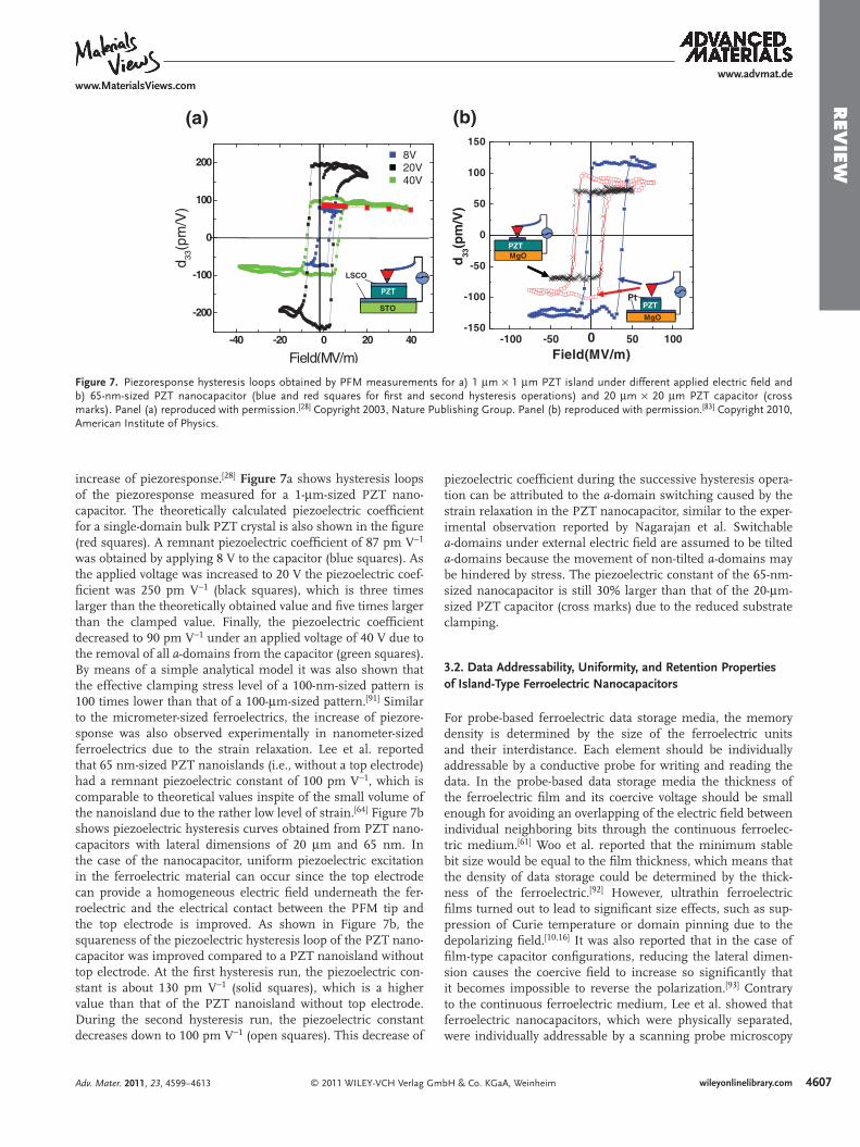
Figure 7 . Piezoresponse hysteresis loops obtained by PFM measurements for a) 1 μ m × 1 μ m PZT island under different applied electric fi eld and b) 65-nm-sized PZT nanocapacitor (blue and red squares for fi rst and second hysteresis operations) and 20 μ m × 20 μ m PZT capacitor (cross marks). Panel (a) reproduced with permission. [ 28 ] Copyright 2003, Nature Publishing Group. Panel (b) reproduced with permission. [ 83 ] Copyright 2010, American Institute of Physics.
(b)
-50
0
50
100
150
d3
3(p
m/V
)
PZT
MgO
(a)
0
100
200
d 33(p
m/V
)
8V20V40V
-4 -2 0 2 4-150
-100
50
Field(MV/m)
Pt
MgO
PZT
-100 -50 50 100-40 -20 0 20 40
-200
-100
Field(MV/m)
PZT
STO
LSCO
increase of piezoresponse. [ 28 ] Figure 7 a shows hysteresis loops of the piezoresponse measured for a 1- μ m-sized PZT nano-capacitor. The theoretically calculated piezoelectric coeffi cient for a single-domain bulk PZT crystal is also shown in the fi gure (red squares). A remnant piezoelectric coeffi cient of 87 pm V − 1 was obtained by applying 8 V to the capacitor (blue squares). As the applied voltage was increased to 20 V the piezoelectric coef-fi cient was 250 pm V − 1 (black squares), which is three times larger than the theoretically obtained value and fi ve times larger than the clamped value. Finally, the piezoelectric coeffi cient decreased to 90 pm V − 1 under an applied voltage of 40 V due to the removal of all a -domains from the capacitor (green squares). By means of a simple analytical model it was also shown that the effective clamping stress level of a 100-nm-sized pattern is 100 times lower than that of a 100- μ m-sized pattern. [ 91 ] Similar to the micrometer-sized ferroelectrics, the increase of piezore-sponse was also observed experimentally in nanometer-sized ferroelectrics due to the strain relaxation. Lee et al. reported that 65 nm-sized PZT nanoislands (i.e., without a top electrode) had a remnant piezoelectric constant of 100 pm V − 1 , which is comparable to theoretical values inspite of the small volume of the nanoisland due to the rather low level of strain. [ 64 ] Figure 7 b shows piezoelectric hysteresis curves obtained from PZT nano-capacitors with lateral dimensions of 20 μ m and 65 nm. In the case of the nanocapacitor, uniform piezoelectric excitation in the ferroelectric material can occur since the top electrode can provide a homogeneous electric fi eld underneath the fer-roelectric and the electrical contact between the PFM tip and the top electrode is improved. As shown in Figure 7 b, the squareness of the piezoelectric hysteresis loop of the PZT nano-capacitor was improved compared to a PZT nanoisland without top electrode. At the fi rst hysteresis run, the piezoelectric con-stant is about 130 pm V − 1 (solid squares), which is a higher value than that of the PZT nanoisland without top electrode. During the second hysteresis run, the piezoelectric constant decreases down to 100 pm V − 1 (open squares). This decrease of
© 2011 WILEY-VCH Verlag GmAdv. Mater. 2011, 23, 4599–4613
piezoelectric coeffi cient during the successive hysteresis opera-tion can be attributed to the a -domain switching caused by the strain relaxation in the PZT nanocapacitor, similar to the exper-imental observation reported by Nagarajan et al. Switchable a -domains under external electric fi eld are assumed to be tilted a -domains because the movement of non-tilted a -domains may be hindered by stress. The piezoelectric constant of the 65-nm-sized nanocapacitor is still 30% larger than that of the 20- μ m-sized PZT capacitor (cross marks) due to the reduced substrate clamping.
3.2. Data Addressability, Uniformity, and Retention Properties of Island-Type Ferroelectric Nanocapacitors
For probe-based ferroelectric data storage media, the memory density is determined by the size of the ferroelectric units and their interdistance. Each element should be individually addressable by a conductive probe for writing and reading the data. In the probe-based data storage media the thickness of the ferroelectric fi lm and its coercive voltage should be small enough for avoiding an overlapping of the electric fi eld between individual neighboring bits through the continuous ferroelec-tric medium. [ 61 ] Woo et al. reported that the minimum stable bit size would be equal to the fi lm thickness, which means that the density of data storage could be determined by the thick-ness of the ferroelectric. [ 92 ] However, ultrathin ferroelectric fi lms turned out to lead to signifi cant size effects, such as sup-pression of Curie temperature or domain pinning due to the depolarizing fi eld. [ 10 , 16 ] It was also reported that in the case of fi lm-type capacitor confi gurations, reducing the lateral dimen-sion causes the coercive fi eld to increase so signifi cantly that it becomes impossible to reverse the polarization. [ 93 ] Contrary to the continuous ferroelectric medium, Lee et al. showed that ferroelectric nanocapacitors, which were physically separated, were individually addressable by a scanning probe microscopy
4607bH & Co. KGaA, Weinheim wileyonlinelibrary.com
4608
www.advmat.dewww.MaterialsViews.com
REVIE
W
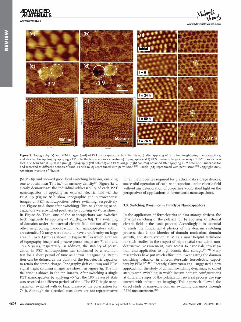
Figure 8 . Topography (a) and PFM images (b–d) of PZT nanocapacitors: b) initial state, c) after applying + 3 V to two neighboring nanocapacitors, and d) after back-poling by applying –3 V onto the left-side nanocapacitor. e) Topography and f) PFM image of large area arrays of PZT nanocapaci-tors. The scan size is 3 μ m × 3 μ m. g) Topography (left column) and PFM image (right column) obtained after applying + 5 V onto one nanocapacitor and recorded at different periods of time. Panels (a–d) reproduced with permission. [ 64 ] Panels (e,f) reproduced with permission. [ 83 ] Copyright 2010, American Institute of Physics.
(SPM) tip and showed good local switching behavior, enabling one to obtain near Tbit in. − 2 of memory density. [ 64 ] Figure 8 a–d clearly demonstrate the individual addressability of each PZT nanocapacitor by applying an external electric fi eld via the PFM tip (Figure 8 a,b show topographic and piezoresponse images of PZT nanocapacitors before switching, respectively, and Figure 8 c,d show after switching). Two neighboring nano-capacitors were switched positively by applying + 3 V dc as shown in Figure 8 c. Then, one of the nanocapacitors was switched back negatively by applying –3 V dc (Figure 8 d). The switching of domains under the external electric fi eld did not affect any other neighboring nanocapacitor. PZT nanocapacitors within an extended 2D array were found to have a uniformity on large area (3 μ m × 3 μ m) as shown in Figure 8 e,f in which z -ranges of topography image and piezoresponse image are 71 nm and 18.2 V (a.u.), respectively. In addition, the stability of polari-zation in PZT nanocapacitors was confi rmed by a retention test for a short period of time as shown in Figure 8 g. Reten-tion can be defi ned as the ability of the ferroelectric capacitor to retain the stored charge. Topography (left column) and PFM signal (right column) images are shown in Figure 8 g. The ini-tial state is shown in the top images. After switching a single PZT nanocapacitor by applying + 5 V dc , the 180 ° reversed state was recorded at different periods of time. The PZT single nano-capacitor, switched with dc bias, preserved the polarization for 74 h. Although the electrical tests above are not representative
© 2011 WILEY-VCH Verlag Gwileyonlinelibrary.com
for all the properties required for practical data storage devices, successful operation of each nanocapacitor under electric fi eld without any deterioration of properties would shed light on the perspectives of applications of ferroelectric nanocapacitors.
3.3. Switching Dynamics in Film-Type Nanocapacitors
In the application of ferroelectrics to data storage devices, the physical switching of the polarization by applying an external electric fi eld is the basic process. Accordingly it is essential to study the fundamental physics of the domain switching process, that is the kinetics of domain nucleation, domain growth, and its relaxation. PFM is a most helpful technique for such studies in the respect of high spatial resolution, non-destructive measurement, easy access to nanoscale investiga-tion, and application to high-density data storage. [ 94–98 ] Many researchers have put much effort into investigating the domain switching behavior in micrometer-scale ferroelectric capaci-tors by PFM. [ 99–107 ] Recently, Gruverman et al. suggested a new approach for the study of domain switching dynamics, so called step-by-step switching in which instant domain confi gurations at different stages of the polarization reversal process are reg-istered with subsequent imaging. This approach allowed the direct study of nanoscale domain switching dynamics through PFM measurement. [ 106 ]
mbH & Co. KGaA, Weinheim Adv. Mater. 2011, 23, 4599–4613
www.advmat.dewww.MaterialsViews.com
REVIE
W
The Kolmogorov–Avrami–Ishibashi (KAI) model is a classical theory based on statistical analysis where nucleation occurs in many different sites and considers the switching process as a phase transformation and rate-limiting parameter. It provides an adequate description of the domain switching dynamics of single crystalline, epitaxially grown, and defect-free ferroelec-tric fi lms. [ 108–111 ] In real ferroelectrics, however, several types of extended defects, including dislocations, domain boundaries, grain boundaries, and oxygen vacancies, exist and therefore the switching behavior does not follow the classical KAI model. Li et al. found that in a ferroelectric epitaxial fi lm with low or zero density of 90 ° domain walls, the switching behavior well obeys the KAI model. However, in a fi lm with a high density of 90 ° domain walls, the movement of 180 ° domain walls was limited, thus the switching kinetics changed to a nucleation-limited model, i.e., non-KAI model. [ 112 ] Jo et al. also investi-gated the polarization switching behavior in (111)-oriented PZT polycrystalline fi lms by pulse measurements. They showed that the experimentally observed switching behavior of domains at the late switching stage deviates from the best fi t of the KAI model prediction and is rather fi tted well with a Lorentzian dis-tribution. They attributed this result to a local fi eld variation in a disordered system due to dipole defects at domain pinning sites. [ 113 ] In addition to macroscopic approaches, Gruverman et al. reported that the switching mechanism of polycrystalline PZT capacitors using the step-by-step PFM approach was found to change from the initial nucleation-dominated process to the lateral domain expansion at later stages, which means that the
© 2011 WILEY-VCH Verlag GmAdv. Mater. 2011, 23, 4599–4613
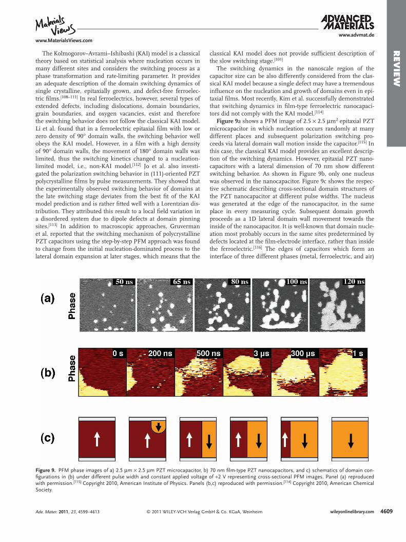
Figure 9 . PFM phase images of a) 2.5 μ m × 2.5 μ m PZT microcapacitor, bfi gurations in (b) under different pulse width and constant applied voltagewith permission. [ 115 ] Copyright 2010, American Institute of Physics. Panels Society.
classical KAI model does not provide suffi cient description of the slow switching stage. [ 101 ]
The switching dynamics in the nanoscale region of the capacitor size can be also differently considered from the clas-sical KAI model because a single defect may have a tremendous infl uence on the nucleation and growth of domains even in epi-taxial fi lms. Most recently, Kim et al. successfully demonstrated that switching dynamics in fi lm-type ferroelectric nanocapaci-tors did not comply with the KAI model. [ 114 ]
Figure 9 a shows a PFM image of 2.5 × 2.5 μ m 2 epitaxial PZT microcapacitor in which nucleation occurs randomly at many different places and subsequent polarization switching pro-ceeds via lateral domain wall motion inside the capacitor. [ 115 ] In this case, the classical KAI model provides an excellent descrip-tion of the switching dynamics. However, epitaxial PZT nano-capacitors with a lateral dimension of 70 nm show different switching behavior. As shown in Figure 9 b, only one nucleus was observed in the nanocapacitor. Figure 9 c shows the respec-tive schematic describing cross-sectional domain structures of the PZT nanocapacitor at different pulse widths. The nucleus was generated at the edge of the nanocapacitor, in the same place in every measuring cycle. Subsequent domain growth proceeds as a 1D lateral domain wall movement towards the inside of the nanocapacitor. It is well-known that domain nucle-ation most probably occurs in the same sites predetermined by defects located at the fi lm-electrode interface, rather than inside the ferroelectric. [ 116 ] The edges of capacitors which form an interface of three different phases (metal, ferroelectric, and air)
4609bH & Co. KGaA, Weinheim wileyonlinelibrary.com
) 70 nm fi lm-type PZT nanocapacitors, and c) schematics of domain con- of + 2 V representing cross-sectional PFM images. Panel (a) reproduced (b,c) reproduced with permission. [ 114 ] Copyright 2010, American Chemical
4610
www.advmat.dewww.MaterialsViews.com
REVIE
W
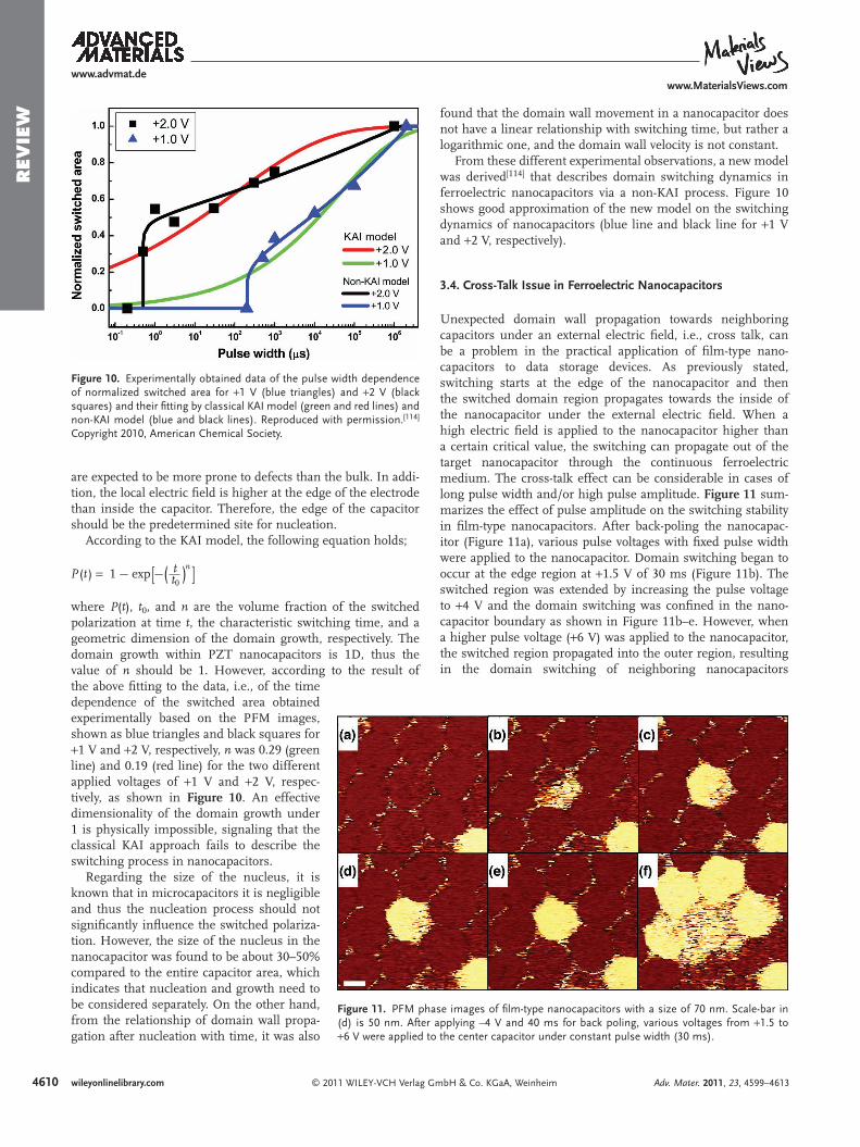
Figure 10 . Experimentally obtained data of the pulse width dependence of normalized switched area for + 1 V (blue triangles) and + 2 V (black squares) and their fi tting by classical KAI model (green and red lines) and non-KAI model (blue and black lines). Reproduced with permission. [ 114 ] Copyright 2010, American Chemical Society.
are expected to be more prone to defects than the bulk. In addi-tion, the local electric fi eld is higher at the edge of the electrode than inside the capacitor. Therefore, the edge of the capacitor should be the predetermined site for nucleation.
According to the KAI model, the following equation holds;
P(t) = 1 − exp[−( t
t0)n ]
where P(t) , t 0 , and n are the volume fraction of the switched polarization at time t , the characteristic switching time, and a geometric dimension of the domain growth, respectively. The domain growth within PZT nanocapacitors is 1D, thus the value of n should be 1. However, according to the result of
Figure 11 . PFM phase images of fi lm-type nanocapacitors with a size of 70 nm. Scale-bar in (d) is 50 nm. After applying –4 V and 40 ms for back poling, various voltages from + 1.5 to + 6 V were applied to the center capacitor under constant pulse width (30 ms).
the above fi tting to the data, i.e., of the time dependence of the switched area obtained experimentally based on the PFM images, shown as blue triangles and black squares for + 1 V and + 2 V, respectively, n was 0.29 (green line) and 0.19 (red line) for the two different applied voltages of + 1 V and + 2 V, respec-tively, as shown in Figure 10 . An effective dimensionality of the domain growth under 1 is physically impossible, signaling that the classical KAI approach fails to describe the switching process in nanocapacitors.
Regarding the size of the nucleus, it is known that in microcapacitors it is negligible and thus the nucleation process should not signifi cantly infl uence the switched polariza-tion. However, the size of the nucleus in the nanocapacitor was found to be about 30–50% compared to the entire capacitor area, which indicates that nucleation and growth need to be considered separately. On the other hand, from the relationship of domain wall propa-gation after nucleation with time, it was also
© 2011 WILEY-VCH Verlag Gwileyonlinelibrary.com
found that the domain wall movement in a nanocapacitor does not have a linear relationship with switching time, but rather a logarithmic one, and the domain wall velocity is not constant.
From these different experimental observations, a new model was derived [ 114 ] that describes domain switching dynamics in ferroelectric nanocapacitors via a non-KAI process. Figure 10 shows good approximation of the new model on the switching dynamics of nanocapacitors (blue line and black line for + 1 V and + 2 V, respectively).
3.4. Cross-Talk Issue in Ferroelectric Nanocapacitors
Unexpected domain wall propagation towards neighboring capacitors under an external electric fi eld, i.e., cross talk, can be a problem in the practical application of fi lm-type nano-capacitors to data storage devices. As previously stated, switching starts at the edge of the nanocapacitor and then the switched domain region propagates towards the inside of the nanocapacitor under the external electric fi eld. When a high electric fi eld is applied to the nanocapacitor higher than a certain critical value, the switching can propagate out of the target nanocapacitor through the continuous ferroelectric medium. The cross-talk effect can be considerable in cases of long pulse width and/or high pulse amplitude. Figure 11 sum-marizes the effect of pulse amplitude on the switching stability in fi lm-type nanocapacitors. After back-poling the nanocapac-itor (Figure 11 a), various pulse voltages with fi xed pulse width were applied to the nanocapacitor. Domain switching began to occur at the edge region at + 1.5 V of 30 ms (Figure 11 b). The switched region was extended by increasing the pulse voltage to + 4 V and the domain switching was confi ned in the nano-capacitor boundary as shown in Figure 11 b–e. However, when a higher pulse voltage ( + 6 V) was applied to the nanocapacitor, the switched region propagated into the outer region, resulting in the domain switching of neighboring nanocapacitors
mbH & Co. KGaA, Weinheim Adv. Mater. 2011, 23, 4599–4613
www.advmat.dewww.MaterialsViews.com
REVIE
W
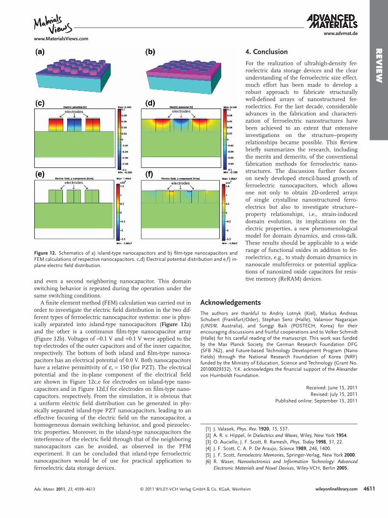
Figure 12 . Schematics of a) island-type nanocapacitors and b) fi lm-type nanocapacitors and FEM calculations of respective nanocapacitors. c,d) Electrical potential distribution and e,f) in-plane electric fi eld distribution.
and even a second neighboring nanocapacitor. This domain switching behavior is repeated during the operation under the same switching conditions.
A fi nite element method (FEM) calculation was carried out in order to investigate the electric fi eld distribution in the two dif-ferent types of ferroelectric nanocapacitor systems: one is phys-ically separated into island-type nanocapacitors ( Figure 12 a) and the other is a continuous fi lm-type nanocapacitor array (Figure 12 b). Voltages of –0.1 V and + 0.1 V were applied to the top electrodes of the outer capacitors and of the inner capacitor, respectively. The bottom of both island and fi lm-type nanoca-pacitors has an electrical potential of 0.0 V. Both nanocapacitors have a relative permittivity of ε r = 150 (for PZT). The electrical potential and the in-plane component of the electrical fi eld are shown in Figure 12 c,e for electrodes on island-type nano-capacitors and in Figure 12 d,f for electrodes on fi lm-type nano-capacitors, respectively. From the simulation, it is obvious that a uniform electric fi eld distribution can be generated in phy-sically separated island-type PZT nanocapacitors, leading to an effective focusing of the electric fi eld on the nanocapacitor, a homogeneous domain switching behavior, and good piezoelec-tric properties. Moreover, in the island-type nanocapacitors the interference of the electric fi eld through that of the neighboring nanocapacitors can be avoided, as observed in the PFM experiment. It can be concluded that island-type ferroelectric nanocapacitors would be of use for practical application to ferroelectric data storage devices.
© 2011 WILEY-VCH Verlag GmbH & Co. KGaA, WeinhAdv. Mater. 2011, 23, 4599–4613
4. Conclusion
For the realization of ultrahigh-density fer-roelectric data storage devices and the clear understanding of the ferroelectric size effect, much effort has been made to develop a robust approach to fabricate structurally well-defi ned arrays of nanostructured fer-roelectrics. For the last decade, considerable advances in the fabrication and characteri-zation of ferroelectric nanostructures have been achieved to an extent that extensive investigations on the structure–property relationships became possible. This Review briefl y summarizes the research, including the merits and demerits, of the conventional fabrication methods for ferroelectric nano-structures. The discussion further focuses on newly developed stencil-based growth of ferroelectric nanocapacitors, which allows one not only to obtain 2D-ordered arrays of single crystalline nanostructured ferro-electrics but also to investigate structure–property relationships, i.e., strain-induced domain evolution, its implications on the electric properties, a new phenomenological model for domain dynamics, and cross-talk. These results should be applicable to a wide range of functional oxides in addition to fer-roelectrics, e.g., to study domain dynamics in nanoscale multiferroics or potential applica-tions of nanosized oxide capacitors for resis-tive memory (ReRAM) devices.
Acknowledgements The authors are thankful to Andriy Lotnyk (Kiel), Markus Andreas Schubert (Frankfurt/Oder), Stephan Senz (Halle), Valanoor Nagarajan (UNSW, Australia), and Sunggi Baik (POSTECH, Korea) for their encouraging discussions and fruitful cooperations and to Volker Schmidt (Halle) for his careful reading of the manuscript. This work was funded by the Max Planck Society, the German Research Foundation DFG (SFB 762), and Future-based Technology Development Program (Nano Fields) through the National Research Foundation of Korea (NRF) funded by the Ministry of Education, Science and Technology (Grant No. 20100029332). Y.K. acknowledges the fi nancial support of the Alexander von Humboldt Foundation.
Received: June 15, 2011 Revised: July 15, 2011
Published online: September 15, 2011
[ 1 ] J. Valasek , Phys. Rev. 1920 , 15 , 537 . [ 2 ] A. R. v. Hippel , In Dielectrics and Waves , Wiley , New York 1954 . [ 3 ] O. Auciello , J. F. Scott , R. Ramesh , Phys. Today 1998 , 51 , 22 . [ 4 ] J. F. Scott , C. A. P. De Araujo , Science 1989 , 246 , 1400 . [ 5 ] J. F. Scott , Ferroelectric Memories , Springer-Verlag , New York 2000 . [ 6 ] R. Waser , Nanoelectronics and Information Technology: Advanced
Electronic Materials and Novel Devices , Wiley-VCH , Berlin 2005 .
4611eim wileyonlinelibrary.com
4612
www.advmat.dewww.MaterialsViews.com
REVIE
W
[ 7 ] K. Uchino , Ferroelectric Devices , Decker , New York 2000 . [ 8 ] M. Dawber , K. M. Rabe , J. F. Scott , Rev. Mod. Phys. 2005 , 77 , 1083 . [ 9 ] J. F. Scott , Science 2007 , 315 , 954 . [ 10 ] V. Nagarajan , J. Junquera , J. Q. He , C. L. Jia , R. Waser , K. Lee ,Y. K. Kim , S. Baik , T. Zhao , R. Ramesh , P. Ghosez , K. M. Rabe , J. Appl. Phys. 2006 , 100 , 051609 .
[ 11 ] C. Lichtensteiger , J. M. Triscone , J. Junquera , P. Ghosez , Phys. Rev. Lett. 2005 , 94 .
[ 12 ] J. Junquera , P. Ghosez , Nature 2003 , 422 , 506 . [ 13 ] V. Nagarajan , I. G. Jenkins , S. P. Alpay , H. Li , S. Aggarwal ,
L. Salamanca-Riba , A. L. Roytburd , R. Ramesh , J. Appl. Phys. 1999 , 86 , 595 .
[ 14 ] M. Stengel , D. Vanderbilt , N. A. Spaldin , Nat. Mater. 2009 , 8 , 392 . [ 15 ] C. L. Jia , S. B. Mi , K. Urban , I. Vrejoiu , M. Alexe , D. Hesse , Nat.
Mater. 2008 , 7 , 57 . [ 16 ] S. K. Streiffer , J. A. Eastman , D. D. Fong , C. Thompson ,
A. Munkholm , M. V. R. Murty , O. Auciello , G. R. Bai , G. B. Stephenson , Phys. Rev. Lett. 2002 , 89 , 067602 .
[ 17 ] D. D. Fong , G. B. Stephenson , S. K. Streiffer , J. A. Eastman , O. Auciello , P. H. Fuoss , C. Thompson , Science 2004 , 304 , 1650 .
[ 18 ] R. Waser , A. Rüdiger , Nat. Mater. 2004 , 3 , 81 . [ 19 ] Y. G. Wang , W. L. Zhong , P. L. Zhang , Phys. Rev. B 1995 , 51 , 5311 . [ 20 ] Y. G. Wang , W. L. Zhong , P. L. Zhang , Phys. Rev. B 1995 , 51 ,
17235 . [ 21 ] R. Kretschmer , K. Binder , Phys. Rev. B 1979 , 20 , 1065 . [ 22 ] S. P. Li , J. A. Eastman , Z. Li , C. M. Foster , R. E. Newnham ,
L. E. Cross , Phys. Lett. A 1996 , 212 , 341 . [ 23 ] I. Vrejoiu , M. Alexe , D. Hesse , U. Gösele , J. Vac. Sci. Technol. B
2009 , 27 , 498 . [ 24 ] M. Alexe , C. Harnagea , D. Hesse , J. Electroceram. 2004 , 12 , 69 . [ 25 ] A. Rudiger , T. Schneller , A. Roelofs , S. Tiedke , T. Schmitz , R. Waser ,
Appl. Phys. A: Mater. Sci. Process. 2005 , 80 , 1247 . [ 26 ] C. S. Ganpule , A. Stanishevsky , Q. Su , S. Aggarwal , J. Melngailis ,
E. Williams , R. Ramesh , Appl. Phys. Lett. 1999 , 75 , 409 . [ 27 ] V. Nagarajan , A. Stanishevsky , R. Ramesh , Nanotechnology 2006 ,
17 , 338 . [ 28 ] V. Nagarajan , A. Roytburd , A. Stanishevsky , S. Prasertchoung ,
T. Zhao , L. Chen , J. Melngailis , O. Auciello , R. Ramesh , Nat. Mater. 2003 , 2 , 43 .
[ 29 ] A. Schilling , D. Byrne , G. Catalan , K. G. Webber , Y. A. Genenko , G. S. Wu , J. F. Scott , J. M. Gregg , Nano Lett. 2009 , 9 , 3359 .
[ 30 ] M. Alexe , C. Harnagea , D. Hesse , U. Gösele , Appl. Phys. Lett. 1999 , 75 , 1793 .
[ 31 ] M. Alexe , C. Harnagea , D. Hesse , U. Gösele , Appl. Phys. Lett. 2001 , 79 , 242 .
[ 32 ] M. Alexe , C. Harnagea , W. Erfurth , D. Hesse , U. Gösele , Appl. Phys. A: Mater. Sci. Process. 2000 , 70 , 247 .
[ 33 ] S. Bühlmann , B. Dwir , J. Baborowski , P. Muralt , Appl. Phys. Lett. 2002 , 80 , 3195 .
[ 34 ] K. Lee , S. Baik , Ann. Rev. Mater. Res. 2006 , 36 , 81 . [ 35 ] C. Harnagea , M. Alexe , J. Schilling , J. Choi , R. B. Wehrspohn ,
D. Hesse , U. Gösele , Appl. Phys. Lett. 2003 , 83 , 1827 . [ 36 ] A. Seifert , A. Vojta , J. S. Speck , F. F. Lange , J. Mater. Res. 1996 , 11 ,
1470 . [ 37 ] M. Alexe , D. Hesse , J. Mater. Sci. 2006 , 41 , 1 . [ 38 ] I. Szafraniak , M. W. Chu , C. Harnagea , R. Scholz , D. Hesse ,
M. Alexe , Integr. Ferroelectr. 2004 , 61 , 231 . [ 39 ] I. Szafraniak , S. Bhattacharyya , C. Harnagea , R. Scholz , M. Alexe ,
Integr. Ferroelectr. 2004 , 68 , 279 . [ 40 ] A. Roelofs , T. Schneller , K. Szot , R. Waser , Nanotechnology 2003 ,
14 , 250 . [ 41 ] I. Szafraniak , C. Harnagea , R. Scholz , S. Bhattacharyya , D. Hesse ,
M. Alexe , Appl. Phys. Lett. 2003 , 83 , 2211 . [ 42 ] A. Roelofs , I. Schneller , K. Szot , R. Waser , Appl. Phys. Lett. 2002 , 81 ,
5231 .
© 2011 WILEY-VCH Verlagwileyonlinelibrary.com
[ 43 ] H. Fujisawa , M. Okaniwa , H. Nonomura , M. Shimizu , H. Niu , J. Eur. Ceram. Soc. 2004 , 24 , 1641 .
[ 44 ] M. Shimizu , N. Nonomura , H. Fujisawa , H. Niu , K. Honda , Integr. Ferroelectr. 2004 , 62 , 109 .
[ 45 ] H. Han , K. Lee , W. Lee , M. Alexe , D. Hesse , S. Baik , J. Mater. Sci. 2009 , 44 , 5167 .
[ 46 ] M. W. Chu , I. Szafraniak , R. Scholz , C. Harnagea , D. Hesse , M. Alexe , U. Gosele , Nat. Mater. 2004 , 3 , 87 .
[ 47 ] S. H. Ahn , S. K. Choi , Appl. Phys. Lett. 2008 , 93 , 113102 . [ 48 ] I. Szafraniak , M. Alexe , Ferroelectrics 2003 , 291 , 19 . [ 49 ] S. Bühlmann , P. Muralt , S. Von Allmen , Appl. Phys. Lett. 2004 , 84 ,
2614 . [ 50 ] W. Lee , M. Alexe , K. Nielsch , U. Gösele , Chem. Mater. 2005 , 17 ,
3325 . [ 51 ] S. K. Lee , W. Lee , M. Alexe , K. Nielsch , D. Hesse , U. Gösele , Appl.
Phys. Lett. 2005 , 86 , 152906 . [ 52 ] S. K. Lee , D. Hesse , M. Alexe , W. Lee , K. Nielsch , U. Gösele , J.
Appl. Phys. 2005 , 98 , 124302 . [ 53 ] W. H. Ma , D. Hesse , U. Gösele , Small 2005 , 1 , 837 . [ 54 ] W. H. Ma , D. Hesse , Appl. Phys. Lett. 2004 , 85 , 3214 . [ 55 ] H. Han , R. Ji , Y. J. Park , S. K. Lee , G. Le Rhun , M. Alexe ,
K. Nielsch , D. Hesse , U. Gösele , S. Baik , Nanotechnology 2009 , 20 , 015301 .
[ 56 ] S. Clemens , T. Schneller , A. van der Hart , F. Peter , R. Waser , Adv. Mater. 2005 , 17 , 1357 .
[ 57 ] S. Kronholz , S. Rathgeber , S. Karthäuser , H. Kohlstedt , S. Clemens , T. Schneller , Adv. Funct. Mater. 2006 , 16 , 2346 .
[ 58 ] Y. Kim , H. Han , Y. Kim , W. Lee , M. Alexe , S. Baik , J. K. Kim , Nano Lett. 2010 , 10 , 2141 .
[ 59 ] H. Nonomura , H. Fujisawa , M. Shimizu , H. Niu , K. Honda , Jpn. J. Appl. Phys. 2003 , 42 , 5918 .
[ 60 ] M. W. Chu , I. Szafraniak , D. Hesse , M. Alexe , U. Gösele , Phys. Rev. B 2005 , 72 .
[ 61 ] P. R. Evans , X. H. Zhu , P. Baxter , M. McMillen , J. McPhillips , F. D. Morrison , J. F. Scott , R. J. Pollard , R. M. Bowman , J. M. Gregg , Nano Lett. 2007 , 7 , 1134 .
[ 62 ] E. J. Mele , Am. J. Phys. 2001 , 69 , 557 . [ 63 ] S. V. Kalinin , E. Karapetian , M. Kachanov , Phys. Rev. B 2004 , 70 . [ 64 ] W. Lee , H. Han , A. Lotnyk , M. A. Schubert , S. Senz , M. Alexe ,
D. Hesse , S. Baik , U. Gösele , Nat. Nanotechnol. 2008 , 3 , 402 . [ 65 ] A. P. Li , F. Muller , A. Birner , K. Nielsch , U. Gösele , J. Appl. Phys.
1998 , 84 , 6023 . [ 66 ] D. Damjanovic , Rep. Prog. Phys. 1998 , 61 , 1267 . [ 67 ] M. E. Lines , A. M. Glass , Principles and Applications of Ferroelectrics
and Related Materials , Clarendon Press , Oxford 1982 . [ 68 ] W. Pompe , X. Gong , Z. Suo , J. S. Speck , J. Appl. Phys. 1993 , 74 ,
6012 . [ 69 ] S. Nambu , D. A. Sagala , Phys. Rev. B 1994 , 50 , 5838 . [ 70 ] R. Ramesh , T. Sands , V. G. Keramidas , Appl. Phys. Lett. 1993 , 63 ,
731 . [ 71 ] Y. Xu , Ferroelectric Materials and Their Applications , Elsevier Science ,
Amsterdam 1993 . [ 72 ] K. S. Lee , J. H. Choi , J. Y. Lee , S. Baik , J. Appl. Phys. 2001 , 90 ,
4095 . [ 73 ] S. V. Kalinin , S. Jesse , B. J. Rodriguez , K. Seal , A. P. Baddorf ,
T. Zhao , Y. H. Chu , R. Ramesh , E. A. Eliseev , A. N. Morozovska , B. Mirman , E. Karapetian , Jpn. J. Appl. Phys. 2007 , 46 , 5674 .
[ 74 ] S. V. Kalinin , A. N. Morozovska , L. Q. Chen , B. J. Rodriguez , Rep. Prog. Phys. 2010 , 73 , 056502 .
[ 75 ] S. Jesse , B. J. Rodriguez , S. Choundhury , A. P. Baddorf , I. Vrejoiu , D. Hesse , M. Alexe , E. A. Eliseev , A. N. Morozovska , J. Zhang , L. Q. Chen , S. V. Kalinin , Nat. Mater. 2008 , 7 , 209 .
[ 76 ] B. J. Rodriguez , S. Jesse , M. Alexe , S. V. Kalinin , Adv. Mater. 2008 , 20 , 109 .
[ 77 ] A. Gruverman , J. Mater. Sci. 2009 , 44 , 5182 .
GmbH & Co. KGaA, Weinheim Adv. Mater. 2011, 23, 4599–4613
www.advmat.dewww.MaterialsViews.com
REVIE
W
[ 78 ] A. Gruverman , A. Kholkin , Rep. Prog. Phys. 2006 , 69 , 2443 . [ 79 ] A. Gruverman , D. Wu , H. J. Fan , I. Vrejoiu , M. Alexe , R. J. Harrison ,
J. F. Scott , J. Phys.: Condens. Matter 2008 , 20 , 342201 . [ 80 ] A. Schilling , R. M. Bowman , G. Catalan , J. F. Scott , J. M. Gregg ,
Nano Lett. 2007 , 7 , 3787 . [ 81 ] A. Schilling , D. Byrne , G. Catalan , K. G. Webber , Y. A. Genenko ,
G. S. Wu , J. F. Scott , J. M. Gregg , Nano Lett. 2009 , 9 , 3359 . [ 82 ] G. Catalan , A. Schilling , J. F. Scott , J. M. Gregg , J. Phys.: Condens.
Matter 2007 , 19 , 132201. [ 83 ] H. Han , Y. J. Park , S. Baik , W. Lee , M. Alexe , D. Hesse , U. Gösele , J.
Appl. Phys. 2010 , 108 , 044102 . [ 84 ] K. Lee , H. Yi , W. H. Park , Y. K. Kim , S. Baik , J. Appl. Phys. 2006 , 100 ,
051615 . [ 85 ] F. Xu , S. Trolier-McKinstry , W. Ren , B. M. Xu , Z. L. Xie , K. J. Hemker ,
J. Appl. Phys. 2001 , 89 , 1336 . [ 86 ] A. L. Kholkin , E. K. Akdogan , A. Safari , P. F. Chauvy , N. Setter , J.
Appl. Phys. 2001 , 89 , 8066 . [ 87 ] K. S. Lee , Y. K. Kim , S. Baik , J. Kim , I. S. Jung , Appl. Phys. Lett.
2001 , 79 , 2444 . [ 88 ] Y. K. Kim , H. Morioka , R. Ueno , S. Yokoyama , H. Funakubo , Appl.
Phys. Lett. 2005 , 86 , 212905 . [ 89 ] Y. K. Kim , H. Morioka , R. Ueno , S. Yokoyama , H. Funakubo , K. Lee ,
S. Baik , Appl. Phys. Lett. 2006 , 88 , 252904 . [ 90 ] G. Le Rhun , I. Vrejoiu , L. Pintilie , D. Hesse , M. Alexe , U. Gösele ,
Nanotechnology 2006 , 17 , 3154 . [ 91 ] V. Nagarajan , Appl. Phys. Lett. 2005 , 87 , 242905 . [ 92 ] J. Woo , S. Hong , N. Setter , H. Shin , J. U. Jeon , Y. E. Pak , K. No , J.
Vac. Sci. Technol. B 2001 , 19 , 818 . [ 93 ] N. Ng , R. Ahluwalia , H. B. Su , F. Boey , Acta Mater. 2009 , 57 , 2047 . [ 94 ] K. Terabe , M. Nakamura , S. Takekawa , K. Kitamura , S. Higuchi ,
Y. Gotoh , Y. Cho , Appl. Phys. Lett. 2003 , 82 , 433 . [ 95 ] A. Gruverman , in Encycolpedia of Nanoscience and Nanotechnology ,
Vol. 3 (Ed: H. S. Nalwa ), American Scientifi c Publisher , Los Angeles 2004 , 359 .
[ 96 ] S. Hong , J. Woo , H. Shin , J. U. Jeon , Y. E. Pak , E. L. Colla , N. Setter , E. Kim , K. No , J. Appl. Phys. 2001 , 89 , 1377 .
© 2011 WILEY-VCH Verlag GAdv. Mater. 2011, 23, 4599–4613
[ 97 ] S. Hong , N. Park , Scanning Probe Microscopy: Electrical and Electro-mechanical Phenomena at the Nanoscale , Springer , Berlin 2006 .
[ 98 ] S. V. Kalinin , D. A. Bonnell , Phys. Rev. B 2002 , 65 , 125408 . [ 99 ] S. Hong , E. L. Colla , E. Kim , D. V. Taylor , A. K. Tagantsev , P. Muralt ,
K. No , N. Setter , J. Appl. Phys. 1999 , 86 , 607 . [ 100 ] P. Paruch , T. Tybell , J. M. Triscone , Appl. Phys. Lett. 2001 , 79 , 530 . [ 101 ] A. Gruverman , O. Auciello , H. Tokumoto , Ann. Rev. Mater. Sci.
1998 , 28 , 101 . [ 102 ] J. Li , B. Nagaraj , H. Liang , W. Cao , C. H. Lee , R. Ramesh , Appl.
Phys. Lett. 2004 , 84 , 1174 . [ 103 ] B. J. Rodriguez , R. J. Nemanich , A. Kingon , A. Gruverman ,
S. V. Kalinin , K. Terabe , X. Y. Liu , K. Kitamura , Appl. Phys. Lett. 2005 , 86 , 012609 .
[ 104 ] A. L. Kholkin , C. Wutchrich , D. V. Taylor , N. Setter , Rev. Sci. Instrum. 1996 , 67 , 1935 .
[ 105 ] C. Dehoff , B. J. Rodriguez , A. I. Kingon , R. J. Nemanich , A. Gruverman , J. S. Cross , Rev. Sci. Instrum. 2005 , 76 , 023708 .
[ 106 ] A. Gruverman , B. J. Rodriguez , C. Dehoff , J. D. Waldrep , A. I. Kingon , R. J. Nemanich , J. S. Cross , Appl. Phys. Lett. 2005 , 87 , 082902 .
[ 107 ] A. Gruverman , D. Wu , J. F. Scott , Phys. Rev. Lett. 2008 , 100 , 097601 .
[ 108 ] Y. Ishibashi , Y. Takagi , J. Phys. Soc. Jpn. 1971 , 31 , 506 . [ 109 ] M. Avrami , J. Chem. Phys. 1939 , 7 , 1103 . [ 110 ] A. N. Kolmogorov , Izv. Akad. Nauk USSR; Ser. Math 1937 , 3 , 355 . [ 111 ] Y. Kim , H. Han , B. J. Rodriguez , I. Vrejoiu , W. Lee , S. Baik ,
D. Hesse , M. Alexe , J. Appl. Phys. 2010 , 108 , 042005 . [ 112 ] W. Li , M. Alexe , Appl. Phys. Lett. 2007 , 91 , 262903 . [ 113 ] J. Y. Jo , H. S. Han , J. G. Yoon , T. K. Song , S. H. Kim , T. W. Noh ,
Phys. Rev. Lett. 2007 , 99 , 267602 . [ 114 ] Y. Kim , H. Han , W. Lee , S. Baik , D. Hesse , M. Alexe , Nano Lett.
2010 , 10 , 1266 . [ 115 ] D. Wu , I. Vrejoiu , M. Alexe , A. Gruverman , Appl. Phys. Lett. 2010 ,
96 , 112903 . [ 116 ] D. J. Kim , J. Y. Jo , T. H. Kim , S. M. Yang , B. Chen , Y. S. Kim ,
T. W. Noh , Appl. Phys. Lett. 2007 , 91 , 132903 .
4613mbH & Co. KGaA, Weinheim wileyonlinelibrary.com

![Ferroelectrics - DBK Groupdbkgroup.org/Papers/kell_ast_wff_ferro1_88.pdf · Downloaded By: [The University of Manchester] At: 16:47 28 February 2007 Ferroelectrics, 1988, Vol. 86,](https://img.pdfslide.us/doc/110x75/5b664ebe7f8b9a2f5c8cc6d4/ferroelectrics-dbk-downloaded-by-the-university-of-manchester-at-1647.jpg)