Embed Size (px)
Citation preview
LA-U R- ~- 0 0 -0
Approved for public release distribution is unlimited
Title I Nanoscale Manipulation of Ge Nanowire by ion hammering
Author(s) I S Thomas Picraux LANL SG Choi NREL Golden CO Lucia Romano UF Gainesville Nicholas G Rudawski UF Gainesville Monta R Holworth UF Gainesville Kevin S Jones UF Gainesville
Intended for I Nature Nanotechnology
pLosAlamos NATIONAL LABORATORY --- EST1943 --shy
Los Alamos National Laboratory an affirmative actionequal opportunity employer is operated by the Los Alamos National Security LLC for the National Nuclear Security Administration of the US Department of Energy under contract DE-AC52-06NA25396 By acceptance of this article the publisher recognizes that the US Government retains a nonexclusive royalty-free license to publish or reproduce the published form of this contribution or to allow others to do so for US Government purposes Los Alamos National Laboratory requests that the publisher identify this article as work performed under the auspices of the US Department of Energy Los Alamos National Laboratory strongly supports academic freedom and a researchers right to publish as an institution however the Laboratory does not endorse the viewpoint of a publication or guarantee its technical correctness
Form 836 (706)
Nanoscale manipulation of Ge nanowires by ion hammering
Lucia Romano Nicholas G Rudawski Monta R Holzworth and Kevin S Jones
Department of Materials Science and Engineering University ofFlorida Gainesville FL 32611
USA
S G Choi2 and S T Picraux
Center for Integrated Nanotechnologies Los Alamos National Laboratory Los Alamos NM 87545
USA
1 Present address Departement of Physics and Astronomy University of Catania Italy
2 Present address National Renewable Energy Laboratory Golden CO 80401 USA
corresponding author
Correspondence and requests for materials should be addressed to LR luciaromano(iljcLinfnit KJ kjones(liengufledu TP picrauxlanlgov
Nanoscale manipulation of Ge nanowires by ion hammering by lRomano
1
Nanowires generated considerable interest as nanoscale interconnects and as active
components of both electronic and electromechanical devices However in many cases
manipulation and modification of nanowires are required to realize their full potential It is
essential for instance to control the orientation and positioning of nanowires in some specific
applications This work demonstrates a simple method to reversibly control the shape and the
orientation of Ge nanowires by using ion beams Initially crystalline nanowires were
partially amorphized by 30 keY Ga+-implantation After amorphization viscous flow and
plastic deformation occurred due to the ion hammering effect causing the nanowires to bend
toward the beam direction The bending was reversed multiple times by ion-implanting the
opposite side of the nanowires resulting in straightening of the nanowires and subsequent
bending in the opposite direction This ion hammering effect demonstrates the detailed
manipulation of nanoscale structures is possible through the use of ion irradiation
Crystalline Si and Ge nanowires (NWs) can be grown by vapor-liquid-solid (VLS) epitaxy
with Au catalyst nanoparticles (see Figure la-b) resulting in pillars with nanometer-scale diameters
and high aspect ratios [I] The NWs exhibit exceptional mechanical and electrical properties that
are attractive for a variety of applications [2-7] However manipulation and modification ofNWs is
required for many applications It is highly desirable to be able to manipulate the orientation of
either individual NWs or an entire surface covered with NWs This work investigates the
application of ion beam processing as a new method of controllably and reversibly manipulating the
orientation of a nanowire after it has been grown
The damage from ion irradiation is usually an undesirable phenomenon unless one is
preamorphizing a material like Si prior to doping[8] One might expect that irradiation should have
the same detrimental effects on nanosystems as on bulk solids But recent experiments on electron
or ion irradiation of various nanostructures demonstrate that it can have beneficial effects as well
and these results suggest that electron or ion beams may be used to tailor the structure and
properties ofnanosystems with high precision [9] These studies suggest that ion hammering may
be used to alter surfaces However no demonstrated effect of ion hammering on NWs has been
reported
When an energetic ion penetrates into a solid it loses energy mainly via two independent
processes with the relative magnitude of each process related to the ion velocity i) nuclear energy
loss (Sn) which dominates at low energy and results from a direct transfer of kinetic energy to the
target nuclei (elastic collisions) and ii) electronic energy loss (Se) which prevails at high energy and
Nanoscale manipulation of Ge nanowires by ion hammering by LRomano
2
results from electronic excitation andor ionization of the target atoms (inelastic collisions) [10] It
has been shown that energetic ion bombardment of amorphous thin films results in unsaturable
plastic flow in the form of anisotropic deformation at negligible density change In this case the ion
beam induces ~ompressive (tensile) deformation parallel (perpendicular) to the beam direction for
sufficiently high Se ( 1 keYom) and sufficiently low target temperatures [11] This is known as
the ion hammering effect This phenomenon has been found to occur only in amorphous material
systems including metallic ceramic and polymer glasses thus indicating that it is universal for the
amorphous state [12 13] No deformation occurs in materials that remain crystalline during ion
bombardment The ion-irradiation-induced deformation of amorphous solids has been explained in
terms of a viscoelastic thermal spike model [14] In this model the deformation is attributed to the
high degree of anisotropy of the ion-induced thermal spike For high values of Se a cylindrical
region around the ion track is heated Shear stresses generated by the thermal expansion of the
highly anisotropic heated region then relax resulting in a local in-plane expansion perpendicular to
the ion track which freezes in upon cooling of the thermal spike The macroscopic anisotropic
deformation is thus the result of a large number of individual ion impacts High energy irradiation
experiments indicated an apparent threshold of Se - 1 keVnm below which no deformation would
be expected [15] although Van Dillen et al [16] demonstrated that ion-irradiation at energies as low
as 300 keY (Se - 04 keVnm) can cause dramatic anisotropic plastic deformation in colloidal Si02
particles Since the plastic deformation is maximized when the specimen thickness is much less
than the ion projected range this phenomenon has been observed primarily with high energy (Me V)
ion irradiation in bulk samples There have been no previous reports to our knowledge of the ion
hammering effect in this electronic-energy loss regime below Se = 04 keVnm The present results
(Se - 01 keVnm for 30 keY Ga ions implantation in Ge) indicate that ion hammering is operative
in this low energy regime and thus may playa significant role in altering the structure of nanoscale
materials
The ion hammering effect was observed during Ga+-irradiation ofGe NWs at 30 keY (Seshy
01 keYom) with the beam incident at 45deg relative to the elongated direction of the NWs Figure 2
presents a series of scanning electron microscopy (SEM) images of the gradual and ultimately
spectacular bending of the Ge NWs from Ga+-irradiation to difference doses (Q) in a specific beam
direction (left or right) With the Ga + beam incident from the right with Q= 34x 1013 cm-2 the
NWs initially start to bend slightly towards left as shown in Figure 2b After an ion dose of Q=
15xl014 cm-2 the NWs are almost vertical (see Figure 2c-d) and tending to bend towards the right
(beam direction) The gradual bending towards the beam direction is clearly evident in Figures 2d
and 2e after Q = 31 X 1014 and 61 x1014 cm-2 respectively The deformation is stable The different
Nanoscale manipulation of Ge nanowires by ion hammering by LRomano
3
bending of crystalline and amorphous NWs is summarized schematically in Figure ld-e After
irradiation to Q= 6x 10 14 cm-2 from the right the beam direction was reversed in order to impinge
from the left as indicated by the arrows in Figures 2f - j which correspond to additional doses ofQ 2
= 27x 10 13 - 38x 1014 cm- bull A spectacular reversal of the bending is observed with the NWs
bending towards the beam direction Once again reorienting the beam to impinge from the right
the NWs were once again observed to bend towards the beam as shown in Figures 2k - 0
2corresponding to Q= 30x 10 13 - 80xI014 cm- bull A decrease in NW diameter due to sputtering was
observed for doses greater than 3xl015 cm-2 for the Ga beam perpendicular to the NWs while for the
NWs aligned parallel to the beam direction much higher doses were possible without observable
loss of Ge Thus the NW shape can be manipulated numerous times by the ion hammering effect
without sputtering limitations and is estimated to survive at least twice the 3 cycles demonstrated
above
Ion beam-induced bending effects have been reported for C nanotubes having diameters of a
few to several hundred nanometers [17 18] and for ShN4membranes [19] Park et at [17] have
discussed mechanisms involving dipole-to-field interaction but have concluded that the electric
fields generated are too low to cause the bending Tripathi et at [18] proposed a model to explain
the bending phenomenon which is based on irradiation induced temperature rise and the
temperature gradient produced along the length and breadth of the structure However this model
assumes the material has a negative thermal expansion coefficient whereas Ge has been shown to
have a positive coefficient over a broad temperature range [20] Thus this proposed explanation for
ion bombardment-induced bending ofnanotubes cannot explain the present observations
The amorphization process of the Ge NWs is presented in Figure 3 Figures 3a - c present
SEM and transmission electron microscopy (TEM) images of an as-grown NW indicating a single
crystal of Ge with a diameter of 50 nm and the lt IIIgt axis oriented along the wire direction Partial 2amorphization of the NW was observed after an implanted dose ofQ = 35x 10 13 cm- which was
responsible for the initial bending of the NW away from the beam direction as shown in Figure 3d
Ge is known to exhibit -10 expansion upon amorphization [21] and thus expansion of the
amorphized side is constrained by the crystalline side causing the nanowire initially to bend away
from the beam SEM and TEM imaging indicated that bending looks more accentuated near the top
of the NW this is due to the base being constrained by the substrate Low- and high-resolution
TEM images shown in Figures 3e and 3findicated uniform implantation along one side of the
NW and amorphization of approximately two-thirds of the structure thus indicating that
amorphization proceeds from the beam-exposed side of the implanted NW It should be noted that
NWs are three dimensional structures that can be approximated as a cylinder Therefore the
Nanoscale manipulation of Ge nanowires by ion hammering by LRomano
4
surface exposed to the ion beam is curved and the beam incidence becomes more grazing moving
from the center of the NW towards the side Consequently the implanted ions have a cylindrical
distribution The distribution of 30 ke V Ga + ions implanted at 0deg (45deg) tilt into a planar Ge substrate
covered with 5 nm Ge02 (as observed in Figure3) has a projected range and longitudinal range
straggling of - 18 (14) and 9 (8) nm respectively as calculated by SRIM simulations [22] Thus
simulations predict an amorphous layer -25 nm thick However since TEM analysis is averaged
over the whole NW thickness the measured depth is larger than the SRIM value Ultimately the
NWs were completely amorphized after Q - 10x 1014 cm-2(not shown) in agreement with the
reported bulk Ge amorphization threshold dose by Si+-implantation at 40 keY [23]
Once completely amorphized the NWs exhibit gradual bending towards the ion beam
direction This behavior is analogous to a strip of metal laying on a hard surface bending upward
when struck in the middle by a hammer Moreover this deformation was reversible as NWs bent
towards the right subjected to additional irradiation from the left bend back towards the left Figure
4 shows SEM images of a bending NW at the extreme points of deformation Additionally several
SEM images at different tilt and rotation angles were collected in order to identify the threeshy
dimensional movement of the NWs during bending (not presented) Comparing the three different
extremes presented in Figures 4b - d it was revealed that almost all of the bending occurs directly
toward the ion beam There are however small differences in the NW length (between 10 and 20
) observed between each extreme due to a small amount of torsion that can be caused by a slight
misalignment of the FIB stage after each irradiation step (see methods for details) this effect has
been assumed to negligibly impact the bending process
After the NWs were amorphized by ion-irradiation viscous flow and plastic deformation
occurred during implantation due to the ion hammering effect [24 25] The time (ion dose)
dependence of this bending can be used to infer the local stress based on a viscoelastic thermal
spike model [13] The NW shown in Figure 4 was discretized along the length in order to measure
the progressive bending as a function of the ion beam dose A schematic of the bending of a single
NW is shown in Figure 5a with the Xs and Zs axes corresponding to the substrate normal and inshy
plane directions as viewed two-dimensionally with the ion beam direction B always incident on the
substrate at 45deg with the origin located at the base of the wire Thus B = lt-1 -1gt in vector
notation The shift of each section of the NW has been measured assuming a negligible variation
along the perpendicular direction to the Xs-Zs plane Thus zs(xs) is the displacement of the wire from
the unbent state at position Xs For the NW it is useful to define Xw and Zw as the local Cartesian
axes parallel and perpendicular to the irradiated side of the wire Thus in the unbent state Xs and Zs
are identical to Xw and Zw
Nanoscale manipulation of Ge nanowires by ion hammering by LRomano
5
Since the ion beam and bent NW always remain in the Xs-Zs plane and boundary conditions
require the exposed surface of the wire to be traction-free [26-28] a localized internal normal stress
axxw along Xw in the wire will be generated which causes the deformation and bending of the wires
In the case of a flat planar surface being irradiated with the ion-beam incident at an angle of () the
generated in-plane stress along the direction coinciding with the surface projection of the ion-beam
will eventually reach a steady-state value of -3A17lt1gt2(cos2laquo())- sin2laquo()raquo where A is the deformation
yield 17 is the viscosity of the amorphous substrate and lt1gt is the ion flux The stress is considered
steady-state because the plastic flow behavior of the substrate is not changing with time though
plastic flow is occurring This also corresponds to macroscopic deformation of the substrate not
changing with time For the case of amorphous Ge under the presented irradiation conditions 17
-2x10¹³ Pa-s [2930] and lt1gt = 43x1012 cm-2s-1with A further defined as [26]
A = 0427(~) aSe (1)
5-4v pCp
where v = 028 is the Poisons ratio [31] a = 79x 10-6 Kl is the thermal expansion coefficient [30]
Se = 012 keVnm assuming all energy lost is converted to heat [30] p = 532 gcm3 is the density
[31] and cp = 04 JgK is the heat capacity of amorphous Ge [32] Thus assuming Eq (1) can be
extrapolated down to very low implant energies laquolt -05 GeV) A = 10x10-2nm2 for Ga+shy
implantation at 30 keY into amorphous Ge
For the case of the NWs presented here it is therefore predicted that axxw under steady-state
conditions (wire curvature not changing with time) will be given by
CTXXw = - A 77lt1gt(cos 2 (OJ - sin 2 (OJ) (2)
where () is assumed to be constant over the whole wire and only the bottom half portion of the NW
was used for stress analysis since any imaging misalignment will produce less deviation from the
actual bending behavior than if the whole NW was used The time-dependent nature ofaxxw
a(t)xxw generated in the NW is given by
c-E - (3)a(tLw - ret)
where E = 86 GPa is the Youngs modulus of amorphous Ge [30] c = 25 nm is the wire halfshy
thickness and r(t) is the local radius of curvature of the NW as a function of time t It is evident
from Figures 2 and 4 that () is variable with time due to bending though the lower portion of the
NWs is roughly linear such that () can be reasonably assumed constant over this whole portion of
the wire The measured time- (dose-) dependence ofaxxw [Eq (3)] was compared with the steadyshy
state value [Eq (2)] predicted to result with () at a given value of t (Q) as shown in Figure 5b with
both values considered as averaged over the whole of the lower portion of the NWs and Q Only 29
Nanoscale manipulation of Ge nanowires by ion hammering by LRomano
6
I (L25x 1014 cm2 Q) was considered in this analysis (approximately corresponding to the SEM
images in Figures Ic e) since the NWs were fully amorphized for this regime and the ionshy
hammering effect was homogeneous over the whole wire The error in a()xxw is reflective of the
error in measuring r(1) due to the possibility of minor misalignment during SEM imaging Thus a
10 error in ret) (corresponding to approximately the same relative error in a(1)xx w) was adopted
to sufficiently account for any minor imaging misalignments that may have arisen It appears the
measured stresses are of lower magnitude compared to the predicted steady-state values However
the time- (dose-) dependence of Uxxbullw is similar to the predicted steady-state stress since the
measured stress in the NW increases as the wire continues to bend towards the beam At present
understanding of the evolution of Uxxw in the NWs is not entirely understood but the threeshy
dimensional nature of the NWs and possible though slight misalignment issues during imaging may
have also played a role The much lower magnitude of generated stress compared to steady-state
predictions based on extrapolation of the high energy ion hammering thermal model to this very
low energy regime is noteworthy [26-28] These results demonstrate that the ion hammering effect
is still significant at unanticipatedly [15] low electronic energy loss values (~ 1 keVnm) and thus
relevant for the manipulation of the shape of structures extending into the nanoscale regime
n is evident from Figure 4 that mechanical work is being done on the NWs by the ion beam
The work done on the NW by the ion beam over of the time interval of implantation II I 12 is
given by
12
W = JFbea)t)Vwiret)dt (4) I
where Fbeam (t) is the I-dependent net force acting on the nanowire as generated by the ion beam
and vwire (t) is the I-dependent velocity of the NW measured at the NW center The whole of the
NW was considered for work analysis The nature of Fbeam (I) is dependent on the momentum of an
incoming ion pion = 333x 1020 N-s the time required for an ion to come to rest after impacting the
surface Ires and the number of ions instantaneously absorbed as a function of I Nins() Thus the
force generated on the beam by the impact of a single ion is equal to pion tres with Nins()
approximated as
ltIgt hP(I)(Ozs(t) )NiTA) - ffresl r- w J-- 1 dx (5)
2 0 ax where hp(t) is the projected height of the nanowire as a function of I and w-50 nm is the crossshy
sectional width of the wire Thus Fbeam (I) in vector notation is approximated as
Nanoscale manipulation of Ge nanowires by ion hammering by LRomano
7
- ltIgt hp(ll(OZs(t) )FbeaJt)~ Pion -w f ---1 cUs(-l-l) (6)
2 0 OXs
with typical values of FbeaJt) on the order of~Olx 10-15 N
Numerically computing the integral in Eq (4) for 29S tS 143 s (corresponding to 125x 1014
s QS 6l5x 1014 cm-2 where the NWs have been fully amorphized) produces W= ~ -3 plusmn 1 eV It
should be noted that these values are orders of magnitude lower than the work required to elastically
bend non-irradiated crystalline Si NWs over comparable length scales [33] Therefore our
experiment clearly shows that it is easier to perform mechanical work during ion-irradiation of an
amorphous material compared to the crystalline counterpart due to viscous flow from the ionshy
hammering effect
The ion beam can act like an artists hammer to model the NW shape as desired and thus
loops or springs can be realized by suitably changing the impinging beam location and direction
Using the same procedure it is presumably possible to bend Si NWs (after amorphization) or Si02
NWs However the bending mechanism ofSi NWs as a function of ion dose would show a higher
threshold dose since the amorphization threshold of Si by Ga implantation is higher than Ge
(displacement energy ofSi and Ge are about 15 and 10 eV [34] respectively) Then amorphous Si
NWs would bend with approximately the same dose dependence as the Ge NWs irradiated by
30keV Ga ions since the electronic energy loss Se is of the same order of magnitude for both
materials Moreover silica NWs can bend without the initial step of amorphization since these
NWs can be grown amorphous In this case the capability of directly modifying the NWs shape
may open up vast opportunities for making versatile building blocks for micro- and nanoscale
photonic circuits and components [35] as well as functionalizing photonic glasses on the nanometer
scale
In conclusion the ion hammering effect was observed for low energy ion implantation of
amorphized Ge nanowires Dramatic reversible bending of the wires toward the incident beam
direction was attributed to stresses induced by viscous flow generated from the ion-hammering
effect Such deformation is highly suitable for in situ manipulation of three-dimensional shapes by
focused ion beams Moreover the work produced by the ion beam due to the viscous flow is
significantly lower than the mechanical work necessary to observe similar bending in crystalline
material
Nanoscale manipulation of Ge nanowires by ion hammering by LRomano
8
Methods
Sample preparation
To facilitate the TEM examination the NWs were grown on (111) Si pillars ~ 40~m tall and
~ 2~m in diameter The pillars were prepared by a deep reactive ion etching of a lithographically
patterned Si (111) substrate After forming the pillars the coupons were cleaned with acetone
followed by methanol rinse in order to remove the residual photoresist Even though a small number
of craters were present on the top surface of the pillars flat Si (111) surface regions existing on the
surface which enabled growth of epitaxial Ge NWs on the top of the pillars
Ge NWs were grown epitaxially via the vapor-liquid-solid (VLS) mechanism in a high-vacuum
cold-wall chemical vapor deposition (CYD) system on (111) Si [36] Prior to loading into the CYD
chamber the native oxide on the Si pillars was removed by a dilute hydrofluoric (HF) acid (2 vol
in DI water) dip and acidified Au nanoparticles with the nominal diameter of 50 nm were
dispersed on the coupons The coupons were further outgassed at 200degC inside the CYD chamber
under vacuum (mid 10-8 Torr range) for 5 hours and pre-annealed at 450degC for 10 min immediately
before the growth ofGe NWs The growth ofGe NWs proceeded via a two-step growth where
the growth is initialized at 425degC and subsequently continued at 375degC This procedure is shown to
increase the proportion of vertically aligned Ge NWs while ensuring minimum tapering Ge~
(30 in H2) was used as the process gas with a partial pressure of900 mTorr during the growth
The growth duration was 10 min The Ge NWs grew in the four lt111gt directions with only the
ones grown normal to the surface (ie [111] direction) used in this study
In-situ ion-irradiation
An FEI Strata DB 235 scanning electron microscopefocused ion beam system was used to
perform in-situ ion beam irradiation Electron and ion beams were oriented with an angle of 52deg
between them The stage was rotated in order to vary the ion beam direction with respect to the
NWs The NWs were irradiated at a stage tilt such that the ion beam was incident at 45deg relative to
the vertical of the NWs All irradiations were performed using a 30 keY Ga+ beam with a square
scanning pattern of 38x38 um2 current of 10 pA (corresponding to an ion of flux 3x 10 12 ions cm-2
S-I) dwell time of 01 ~s and beam spot size of30 nm Thus the dose received depended on the
time of exposure and ion beam incidence angle After each irradiation step the stage was tilted and
rotated 52deg and 90deg respectively in order to take SEM images of the NWs perpendicular to the
beam direction
9
Nanoscale manipulation of Ge nanowires by ion hammering by LRomano
Structural characterization
Transmission electron microscopy was used to characterize the structure of the NWs in the
as-grown condition and after ion irradiation The samples were imaged on a JEOL 2010F
transmission electron microscope using on-axis multi-beam imaging conditions The pillar was
attached to an in-situ micromanipulator by selective ion beam Pt deposition and lifted out from the
parent material taking care to avoid any ion beam irradiation of the pillar top in order to protect the
NWs The free pillar was then attached to a special Cu grid and loaded into the microscope for
imaging
Nanoscale manipulation of Ge nanowires by ion hammering by LRomano
10
Acknowledgements
The authors acknowledge the Major Analytical Instrumentation Center at the University of
Florida for use of the transmission electron microscope and focused ion beam facilities and
Clarence Tracy at Arizona Institute ofNanoelectronics (Arizona State University Tempe) for his
work on patterning substrates This work was performed in part at the Center for Integrated
Nanotechnologies a US Department of Energy Office of Basic Energy Sciences user facility at
its Los Alamos National Laboratory (Contract DE-AC52-06NA25396) site
Nanoscale manipulation of Ge nanowires by ion hammering by LRomano
11
References
1 Wagner RS Ellis WC Vapor-Liquid-Solid Mechanism Of Single Crystal Growth Appl
Phys Lett 4 89-90 (1964)
2 Cui Y Lieber C M Functional Nanoscale Electronic Devices Assembled Using Silicon
Nanowire Building Blocks Science 291851-853 (2001)
3 Agarwal P Vijayaraghava M N Neuilly F Hijzen E Hurkx G A M Breakdown
Enhancement in Silicon Nanowire p-n Junctions Nano Lett 7 896-899 (2007)
4 Tian B Zheng X Kempa T J Fang Y Yu N Yu G Huang J Lieber C M
Coaxial silicon nanowires as solar cells and nanoelectronic power sources Nature 449885shy
889 (2007)
5 Koo S M Fujiwara A Han J P Vogel E M Richter C A Bonevich J E High
Inversion Current in Silicon Nanowire Field Effect Transistors Nano Lett 4 2197-2201
(2004)
6 Martinez J Martinez R V and Garcia R Silicon Nanowire Transistors with a Channel
Width of4 nm Fabricated by Atomic Force Microscope Nanolithography Nano Lett 8
3636-3639 (2008)
7 Tribu A Sallen G Aichele TAndre R Poizat JP Bougerol C Tatarenko S andKheng
K A High-Temperature Single-Photon Source from Nanowire Quantum Dots Nano Lett
84326-4329(2008)
8 Robertson LS Jones KS Rubin LM Jackson J Annealing kinetics of 311 defects and
dislocation loops in the end-of-range damage region of ion implanted silicon J Appl Phys
872910-2913 (2000)
9 Krasheninnikov AV and Banhart F Engineering of nanostructured carbon materials with
electron or ion beams Nature Materials 6 723-733 (2007)
10 Ion-solid Interactions Fundamentals and Applications Michael Anthony Nastasi James W
Mayer James Karsten Hirvonen Cambridge University Press 1996
11 KlaumOnzer S and Schumacher G Dramatic Growth ofGlassy PdsoSho during Heavy-Ion
Irradiation Phys Rev Lett 51 1987-1990 (1983)
12 Hedler A KlaumOnzer S L Wesch W Amorphous silicon exhibits a glass transition
Nature Materials 3804-809 (2004)
13 Benyagoub A Loffier S Rammensee M Klaumunzer S and Saemann-Ischenko G
Plastic deformation in Si02 induced by heavy-ion irradiation Nucl lnstrum Methods Phys
Res B 65 228-231 (1992)
Nanoscale manipulation of Ge nanowires by ion hammering by LRomano
12
14 Trinkaus H and Ryazanov AI Viscoelastic Model for the Plastic Flow of Amorphous
Solids under Energetic Ion Bombardment Phys Rev Lett 74 5072-5075 (1995)
15 Snoeks E van Blaaderen A van Dillen T van Kats C M Brongersma M L and Polman
A Colloidal ElliPsoids with Continuously Variable Shape Adv Mater 12 1511-1514
(2000)
16 van Dillen T Polman A van Kats C M Van Blaaderen A Ion beam-induced anisotropic
plastic deformation at 300 ke V Appl Phys Lett 834315-4317 (2003)
17 Park BC Jung KY Song WY Beom-hoan 0 Ahn Sl Bending ofa Carbon Nanotube
in Vacuum Using a Focused Ion Beam Adv Mater 1895-98 (2006)
18 Tripathi SK Shukla N Dhamodaran S Kulkarni V N Controlled manipulation of
carbon nanopillars and cantilevers by focused ion beam Nanotechnology 19205302shy
205307 (2008)
19 Arora WJ Sijbrandij S Stem L Notte l Smith HL Barbastathis G Membrane folding
by helium ion implantation for three-dimensional device fabrication J Vac Sci Technol B
252184-2187(2007)
20 Novikova S I Thermal expansion of crystals (Science Moscow 1974)
21 Stritzker B Elliman R G Zou J Self-ion-induced swelling of germanium Nucl Instrum
Methods Phys B 175 193-196 (2001)
22 Ziegler JF Biersack JP Littmark u in The Stopping and Range oflons in Solids
(Pergamon New York 2003)
23 Hickey D PhD thesis University of Florida (2007)
24 Klaumiinzer S Li C L6ffler S Rammensee M Schumacher G Neitzert HC lonshy
Beam-Induced plastic deformation A universal behavior of amorphous solids Radiat Eff
Def Solids 108 131-135 (1989)
25 Benyagoub A L6ffler S Rammensee M Klaumiinzer S lon-bearn-induced plastic
deformation in vitreous silica Radiat Eff Def Solids 110217-219 (1989)
26 Klaumiinzer S and Benyagoub A Phenomenology of the plastic flow of amorphous solids
induced by heavy-ion bombardment Phys Rev B 437502-7506 (1991)
27 Gutzmann A Klaumiinzer S Meier P lon-Beam-Induced Surface Instability of Glassy
Fe4oNi4oB2o Phys Rev Lett 742256-2259 (1995)
28 Gutzmann A and Klaumiinzer S Shape instability ofamorphous materials during highshy
energy ion bombardment Nucl Instrum Methods Phys Res B 127-128 12-17 (1997)
29 Volkert C A Stress and plastic flow in silicon during amorphization by ion bombardment
J Appl Phys 70 3521-3527 (1991)
Nanoscale manipulation of Ge nanowires by ion hammering by LRomano
13
30 Witvrouw A and Spaepen F Viscosity and elastic constants of amorphous Si and Ge J
Appl Phys 74 7154-7161 (1993)
31 Mathioudakis C and Kelires Pe Softening of elastic moduli ofamorphous
semiconductors J Non-cryst Solids 266 161-165 (2000)
32 Szyszko W Vega F and Afonso C N Shifting of the thermal properties of amorphous
germanium films upon relaxation and crystallization Appl Phys A 61 141-147 (1995)
33 Hoffmann S Utke I Moser B Christiansen S H Schmidt V Go 1 sele U and Ballife
Measurement of the Bending Strength of Vapor-Liquid-Solid Grown Silicon Nanowires
Nano Lett 6 622-625 (2006)
34 Nord J Nordlund K Keinonen J Amorphization mechanism and defect structures in ionshy
beam-amorphized Si Ge and GaAs Phys Rev B 65 (2002) 165329-14
35 Tong R R Gattass J B Ashcom S He J Lou M Shen I Maxwell and E Mazur
Subwavelengthdiameter silica wires for low-loss optical wave guiding Nature 426 816shy
819 (2003)
36 Dailey J W Taraci J Clement T Smith D J Drucker J Picraux S T Vapor-liquidshy
solid growth of germanium nanostructures on silicon J Appl Phys 96 7556-7567 (2004)
Nanoscale manipulation of Ge nanowires by ion hammering by LRomano
14
Figure Legends
Figure 1 Illustration of the effects of ion implantation on nanowires a) VLS growth ofGe
nanowires on (Ill) Si b c) as-grown nanowires with diameters -50 run d) after low dose 30 keY
Ga+ implantation at 45deg (Rp - 20 run) which amorphizes part of the wire (slight bend away due to
lower density of amorphous Ge) and e) ion hammering effect dominates as dose increases causing
the nanowire to bend toward the ion beam
Figure 2 SEM images of three ion irradiation sequences showing reversible bending ofGe
nanowires epitaxially grown on (111) Si during Ga+-irradiation at 30 keY incident at 45deg with
respect to the vertical ofthe nanowires Ion beam incident from the right with Q = a) 0 (as-grown
non-irradiated) b) 34x1013 c) 15x1014
d) 3l x I014 and e) 6lx1014 cm2 Ion beam subsequently
incident from the left on the resulting nanowires with additional Q = t) 27x 1013 g) lOx 1014
h)
16x 1014 i) 32x 1014
andj) 38x 1014 cm2 Ion beam subsequently incident from the right on the
resulting nanowires with Q = k) 30x 1013 1) 15x 1014 m) 34x 1014
n) 49x 1014 and 0) 80x 1014
cm2
Figure 3 Effect of low dose implantation on the side of the nanowire Before implantation a) SEM
image b) low magnification TEM micrograph c) high resolution TEM micrograph After 30 keY
Ga + implantation at 45deg with respect to the nanowire axis at a dose of Q = 35 X 1013 cm2 d) SEM
image e) low magnification TEM micrograph and t) high resolution TEM micrograph Crystalline
(c) amorphous (n) and oxidized (ox) portions of the nanowires are schematically indicated the ion
beam direction is from the right
Figure 4 SEM images showing the reversibility of bending at three different extremes for a single
Ge nanowire during Ga+-irradation at 30 keY a) an as-grown Ge nanowire b) after irradiation from
the right with a dose of Q 61 x1014 cm2 c) after irradiation from the left with Q = 38x 1014 cm2
and d) after irradiation from the right with Q= 80x 1014 cm2 Each value ofadditional dose Q is
given with respect to a specific beam direction (left or right)
Figure 5 a) Schematic discretization of a bending Ge nanowire depicting the coordinate systems
used for the measurement of internal stresses and mechanical work performed during ionshy
irradiation b) Plot of the measured in-plane compressive stress Oxxw (open circles) generated in
the nanowire as determined from the curvature along the bottom portion of the nanowire shown in
Nanoscale manipulation of Ge nanowires by ion hammering by LRomano
15
Figure 4b as a function of ion dose and irradiation time during the initial irradiation step using Eq
(3) The predicted steady-state values ofUn bullw (solid squares) that would be generated in the
NANOWIRE (corresponding to observed irradiation angles at specific times and doses) as predicted
by Eq (2) are provided for reference
Nanoscale manipulation of Ge nanowires by ion hammering by lRomano
16
O Ge
a) O H b)
O Au
(111)Si -------------
Crystalline nanowires Amorphous nanowires
Figure 15 in Nanoscale manipulation of Ge nanowires by ion hammering by LRomano et al
Figure 25 in Nanoscale manipulation of Ge nanowires by ion hammering by LRomano et al
Figure 35 in Nanoscale manipulation of Ge nanowires by ion hammering by LRomano et al
Figure 45 in Nanoscale manipulation of Ge nanowires by ion hammering by LRomano et al
a) Initial b)
+ Ion dose [x1 014 attcm2]
2 3 4 5 6 I I I I I
10 _ bull Predicted Steady-State 1-
1 shy
QQ bullbullQ Q
Qbull +1 z~~ Q middotmiddotmiddot0middotmiddotmiddot Measured -01 shy Q
I I I I I I
20 40 60 80 100 120 140
time [s]
(111) Si Substrate
r~middotl ~-~--~--bull ~ i
I i bullbull
I +
Figure 55 in Nanoscale manipulation of Ge nanowires by ion hammering by LRomano et al
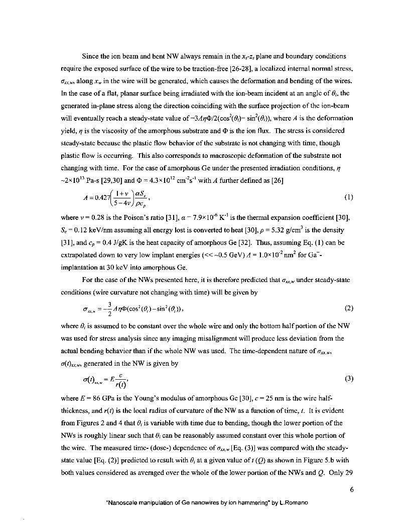
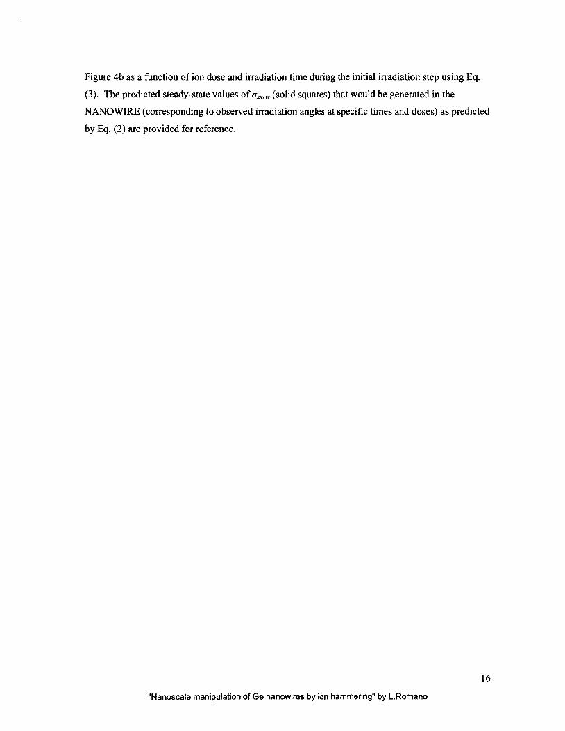
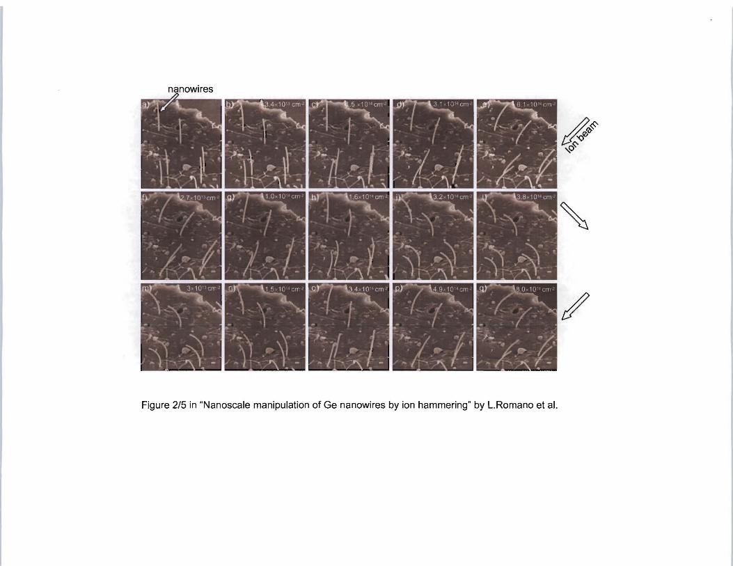
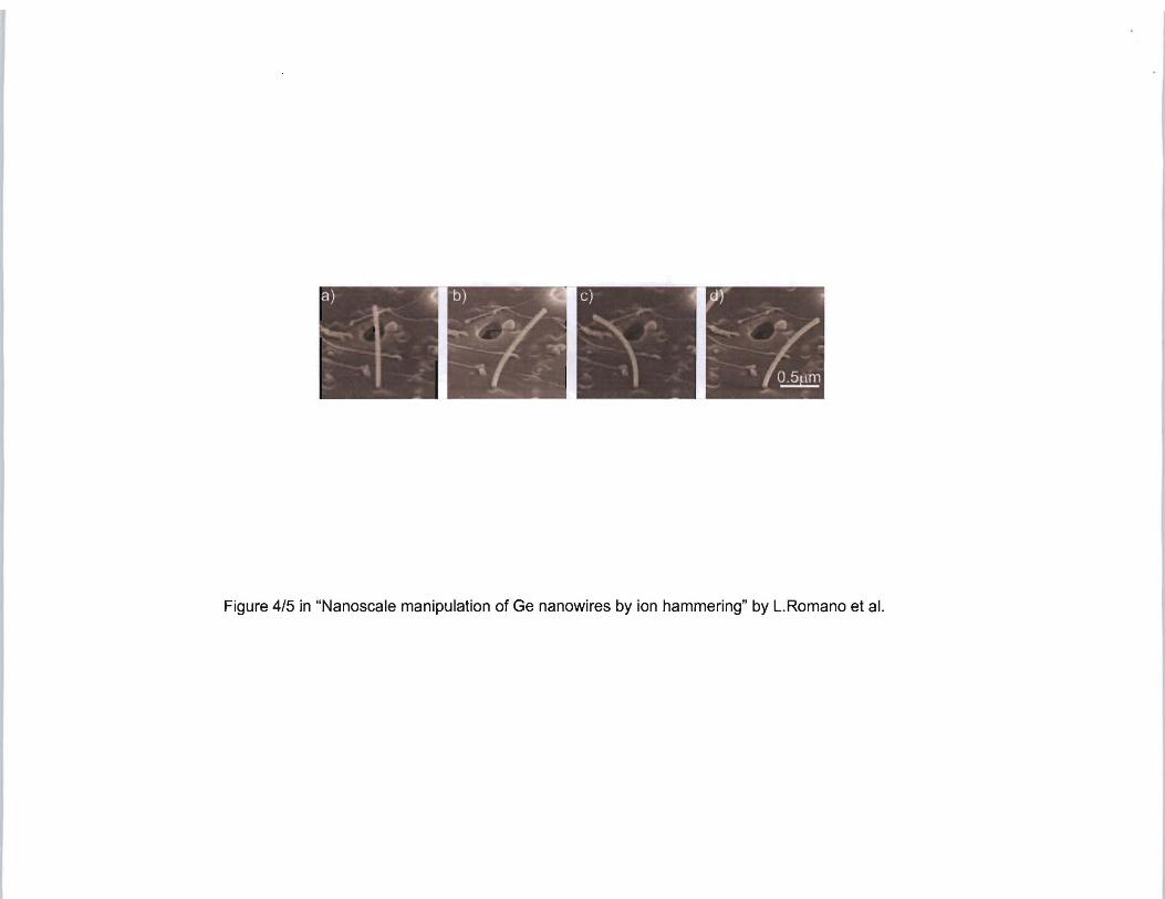


![Lattice Boltzmann modeling of phonon transportin simple nanoscale geometries such as thin films, nanowires and nanotubes [5,16,19,20]. But the rigorous development of widely applicable](https://img.pdfslide.us/doc/110x75/602f396cdb2632238f37a8cd/lattice-boltzmann-modeling-of-phonon-in-simple-nanoscale-geometries-such-as-thin.jpg)