Embed Size (px)
Citation preview
1
Nanometer-scale lateral p-n junctions in graphene/-RuCl3 heterostructures
Daniel J. Rizzo1,†, Sara Shabani1,†, Bjarke S. Jessen1,2,†, Jin Zhang3,†, Alexander S. McLeod1,#,
Carmen Rubio-Verdú1, Francesco L. Ruta1,4, Matthew Cothrine5, Jiaqiang Yan5,6, David G.
Mandrus5,6, Stephen E. Nagler7, Angel Rubio3,8,9,*, James C. Hone3, Cory R. Dean1, Abhay N.
Pasupathy1,10*, D.N. Basov1,*
1Department of Physics, Columbia University, New York, NY, 10027, USA
2Department of Mechanical Engineering, Columbia University, New York, NY, 10027, USA
3Theory Department, Max Planck Institute for Structure and Dynamics of Matter and Center for
Free-Electron Laser Science, 22761 Hamburg, Germany
4Department of Applied Physics and Applied Mathematics, Columbia University, New York, NY,
10027, USA
5Department of Materials Science and Engineering, University of Tennessee, Knoxville,
Tennessee 37996, USA
6Materials Science and Technology Division, Oak Ridge National Laboratory, Oak Ridge,
Tennessee 37831, USA
7Neutron Scattering Division, Oak Ridge National Laboratory, Oak Ridge, Tennessee 37831,
United States
8Center for Computational Quantum Physics, Flatiron Institute, New York, New York 10010, USA
9Nano-Bio Spectroscopy Group, Universidad del País Vasco UPV/EHU, San Sebastián 20018,
Spain
10Condensed Matter Physics and Materials Science Department, Brookhaven National Laboratory,
Upton, NY 11973, USA
†Contributed equally
#Present Address: School of Physics and Astronomy, University of Minnesota, Minneapolis, MN
55455
*Correspondence to: [email protected], [email protected], and
2
Abstract
The ability to create high-quality lateral p-n junctions at nanometer length scales is
essential for the next generation of two-dimensional (2D) electronic and plasmonic devices.
Using a charge-transfer heterostructure consisting of graphene on -RuCl3, we conduct a proof-
of-concept study demonstrating the existence of intrinsic nanoscale lateral p-n junctions in the
vicinity of graphene nanobubbles. Our multi-pronged experimental approach incorporates
scanning tunneling microscopy (STM) and spectroscopy (STS) and scattering-type scanning
near-field optical microscopy (s-SNOM) in order to simultaneously probe both the electronic and
optical responses of nanobubble p-n junctions. Our STM and STS results reveal that p-n
junctions with a band offset of more than 0.6 eV can be achieved over lateral length scale of less
than 3 nm, giving rise to a staggering effective in-plane field in excess of 108 V/m. Concurrent s-
SNOM measurements confirm the utility of these nano-junctions in plasmonically-active media,
and validate the use of a point-scatterer formalism for modeling surface plasmon polaritons
(SPPs). Model ab initio density functional theory (DFT) calculations corroborate our
experimental data and reveal a combination of sub-angstrom and few-angstrom decay processes
dictating the dependence of charge transfer on layer separation. Our study provides experimental
and conceptual foundations for the use of charge-transfer interfaces such as graphene/-RuCl3 to
generate p-n nano-junctions.
3
Introduction
Nanoscale lateral p-n junctions in graphene present promising routes for investigating
fundamental quantum phenomena such as Andreev reflection1,2, whispering gallery mode
resonators3,4, quantum dots5-9, Veselago lensing10,11 and photonic crystals12. The ability to realize
nanoarchitectures capable of hosting these properties relies on precise control over the lateral p-n
junction size – ideally down to atomic length scales. Despite the potential advantages of tailored
nanometer junctions, attempts to realize sharp and clean interfacial junctions in graphene-based
devices have been limited to > 20 nm11,13 and lack the nominal potential profile for yielding
high-quality devices. Conventional techniques such as local back gating14, ion implantation15,16,
and adatoms17 are practically challenging to implement and can be accompanied by an increase
in disorder, reduction in mobility, and surface contamination. Moreover, the maximum charge
carrier density achievable with these approaches is typically limited to less than 51012 cm–2,18,19
restricting the potential gradients accessible with these techniques.
Recent theoretical20,21 and experimental22-25 work on graphene/-RuCl3 heterostructures
demonstrates that the Dirac-point energy (EDirac) in graphene will experience a massive shift
(~0.6 eV) due to work function-mediated interlayer charge transfer with the underlying -RuCl3.
While transport measurements suggest a high degree of interlayer charge transfer23 in
graphene/-RuCl3 heterostructures (>1013 cm–2), they have not revealed the lateral dimensions of
this charging process. On the other hand, analysis of the plasmonic behavior of graphene/-
RuCl3 in the vicinity of nanobubbles suggests that boundaries between highly doped and pristine
graphene are no wider than 50 nm22. Raman maps conducted on these heterostructures produce
similar constraints on the maximum size of lateral charge modulation boundaries24. However, a
4
detailed understanding of the nanoscale spatial dependence of interlayer charge transfer between
graphene and -RuCl3 necessitates use of a high-resolution local probe.
In order to elucidate the intrinsic lateral and vertical length scales associated with
interlayer charge transfer in graphene/-RuCl3 heterostructures, we employ two complementary
imaging and spectroscopic techniques: scanning tunnelling microscopy and spectroscopy
(STM/STS) and scattering-type scanning near-field optical microscopy (s-SNOM). STM and
STS are ideal probes for studying lateral junction interfaces (e.g. p-n , p-p’, p-i-p, etc.) with
atomic resolution and provide information about the local electronic structure (in particular,
EDirac in graphene). On the other hand, s-SNOM uses hybrid light-matter modes known as
surface plasmon polaritons (SPPs) to probe the local conductivity in graphene. This multi-
messenger experimental approach provides a multifaceted view of the fundamental length scales
associated with interlayer charge transfer as encoded in both the electronic and plasmonic
responses of graphene/-RuCl3.
We use nanobubbles that arise spontaneously at the graphene/-RuCl3 heterostructure
interface during fabrication as a testbed for probing the in-plane and out-of-plane behavior of
interlayer charge transfer. Differential conductivity (dI/dV) maps and point spectroscopy
performed at the boundary of nanobubbles reveal that highly p-doped and intrinsically n-doped
graphene are separated by a lateral distance of ~3 nm and vertically by ~0.5 nm, generating
internal fields on the order of 108 V/m that are largely confined to the graphene plane. At the
same time, the rapid change in the graphene conductivity in the vicinity of nanobubbles acts as a
hard plasmonic barrier that reflects SPPs generated during s-SNOM measurements, as observed
previously22. The results of STS measurements inform our interpretation of the s-SNOM data
and permit us to further develop our model for the complex-valued near-field signal in the
5
vicinity of nanobubbles using a perturbative point-scatterer approach. Our results are well
supported by first-principles density-functional theory (DFT) calculations, which reveal the
origin of the sharp spatial profile of interlayer charge transfer at the boundary of nanobubbles.
Results and Discussion
The graphene/-RuCl3 heterostructures studied herein were fabricated using dry transfer
techniques from components isolated using exfoliation from single-crystal sources (see methods
and Fig. S1 for a detailed description of the fabrication process). The resulting heterostructure
consists of large regions of graphene forming a flat interface with the underlying -RuCl3, which
are occasionally interrupted by graphene nanobubbles (Fig. 1A) (see Fig. S2 for STM
topographic overview).
A high magnification topographic STM image of a characteristic graphene nanobubble is
shown in Fig. 1B. As observed with STM topography, the typical heights of nanobubbles studied
in this work were between 1 to 3 nm, while the radius ranged from 20 to 80 nm. Topographic
images collected with an atomic force microscope (AFM) used during s-SNOM measurements
yield similar nanobubble dimensions (Fig. S2). On the other hand, near-field images of these
same nanobubbles collected using s-SNOM reveal larger circular features that extend over lateral
distances of several hundred nanometers (Fig. 1C). The oscillatory nature of the near-field signal
moving radially from nanobubbles is consistent with the presence of SPPs that are either being
launched or reflected from these locations, giving rise to modulations in the near-field signal that
extend far beyond the nanobubble area. It has been suggested that these plasmonic features arise
due to discontinuities in the graphene conductivity associated with local modulation of charge
6
carrier density22, though the precise nature of this profile demands further scrutiny with STM and
STS.
In order to gain insight into the spatial dependence of interlayer charge transfer, we
performed a series of STM and STS measurements in the vicinity of four different graphene
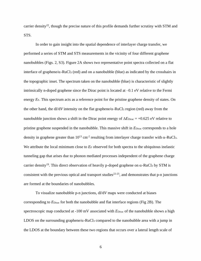
nanobubbles (Figs. 2, S3). Figure 2A shows two representative point spectra collected on a flat
interface of graphene/-RuCl3 (red) and on a nanobubble (blue) as indicated by the crosshairs in
the topographic inset. The spectrum taken on the nanobubble (blue) is characteristic of slightly
intrinsically n-doped graphene since the Dirac point is located at –0.1 eV relative to the Fermi
energy EF. This spectrum acts as a reference point for the pristine graphene density of states. On
the other hand, the dI/dV intensity on the flat graphene/-RuCl3 region (red) away from the
nanobubble junction shows a shift in the Dirac point energy of EDirac = +0.625 eV relative to
pristine graphene suspended in the nanobubble. This massive shift in EDirac corresponds to a hole
density in graphene greater than 1013 cm-2 resulting from interlayer charge transfer with -RuCl3.
We attribute the local minimum close to EF observed for both spectra to the ubiquitous inelastic
tunneling gap that arises due to phonon mediated processes independent of the graphene charge
carrier density19. This direct observation of heavily p-doped graphene on -RuCl3 by STM is
consistent with the previous optical and transport studies22-25, and demonstrates that p-n junctions
are formed at the boundaries of nanobubbles.
To visualize nanobubble p-n junctions, dI/dV maps were conducted at biases
corresponding to EDirac for both the nanobubble and flat interface regions (Fig 2B). The
spectroscopic map conducted at -100 mV associated with EDirac of the nanobubble shows a high
LDOS on the surrounding graphene/-RuCl3 compared to the nanobubble area with a jump in
the LDOS at the boundary between these two regions that occurs over a lateral length scale of
7
approximately 3 nm (Fig. 2C). This is consistent with the expectation that the nanobubble should
have a suppressed LDOS at its EDirac compared to the surrounding highly doped regions. On the
other hand, at +525 meV (i.e. EDirac of the flat graphene/-RuCl3 interface) the LDOS is
enhanced on the nanobubble compared to the surrounding flat graphene/-RuCl3 region due to
the corresponding Dirac point minimum of the latter. A similarly abrupt shift in the LDOS at the
nanobubble edge is observed at this energy (Fig. 2C). This behavior is characteristic of a
nanometer-scale p-n interface in graphene located at the nanobubble boundary.
We then extracted the potential profile across the p-n junction and evaluated its
sharpness. A representative dI/dV line cut is shown in Fig. 2D and follows the cyan trajectory
highlighted in the inset of Fig. 2A. Fig. 2D clearly shows that the local minimum of the Dirac
point shifts abruptly at the boundary of the nanobubble from +0.525 eV to –0.1 eV over a length
scale of only a few nanometers. To provide information about the correspondence between STM
topography and the shift in EDirac, we compare the nanobubble topographic cross-section
(denoted with a cyan dotted line in Fig. 2D) with the Dirac energy position (green dashed line). It
is evident that the change in the graphene doping level occurs much more abruptly than the
height profile of the nanobubble, implying that interlayer charge transfer is rapidly suppressed
with interlayer separation. The lateral junction width is measured to be ~3 nm as indicated by the
partially transparent blue and red rectangle in Fig. 2D. The lateral width of this depletion region
is roughly one order of magnitude smaller than previously reported results on state-of-the-art
split back gate devices13. To provide a step-by-step view of the evolution of EDirac across the
junction, a few spectra from the highlighted region of the line cut are shown in Fig. 2E. These
individual spectra allow us to understand how the doping level develops over the 3 nm transition
at the nanobubble boundary. Once the interface of the nanobubble is reached and the graphene

8
begins to separate from the underlying -RuCl3 layer, the minimum corresponding to the Dirac
point at +0.525 eV rapidly shifts to lower biases. Beyond this point, EDirac shifts more gradually
until it reaches its minimum value of –100 mV. The dependence of the shift in EDirac on the
nanobubble height is shown explicitly in Fig. 4D, hinting that two distinct mechanisms govern
the interlayer charge transfer process, giving rise to two characteristic vertical length scales.
Armed with the results of STM and STS experiments, we now return to s-SNOM images
conducted on graphene nanobubbles. Data were collected on five different nanobubbles over a
frequency range of 930 – 2280 cm–1 (Fig. 3). Characteristic images of the near-field amplitude
and phase for = 990 cm–1 are shown in Fig. 3A along with the associated nanobubble
dimensions. Immediately outside the radius of the nanobubble, radial oscillations of both near-
field channels decay as a function of distance as shown explicitly in the linecuts in Fig. 3C. As
expected22, the spacing between fringes clearly disperses with frequency (Fig. S4). In principle,
these fringes could arise from SPPs generated on and propagating away from nanobubbles (so-
called p fringes), from SPPs generated at the AFM tip that reflect from the nanobubble
boundary (p/2 fringes), or from both. Previous work on similar heterostructures would suggest
the near-field behavior is primarily dominated by the latter22.
To definitively resolve this question, it is useful to consider that the STS data provides
unambiguous evidence that the entirety of the graphene nanobubble consists of nominally
undoped graphene surrounded by highly-doped graphene with a boundary width on the order of
only a few nanometers. We therefore model the s-SNOM data of a graphene nanobubble as a
raster-scanned dipole over a circular conductivity depletion region surrounded by a bulk
possessing high conductivity in a manner similar to our previous study22 (Fig. 3B, see
supplementary discussion for detailed model description). Expanding on this previous work, we
9
now consider that the SPPs generated at the AFM tip during s-SNOM measurements may
possess a wide range of wavelengths relative to the size of the nanobubble. At one extreme, the
SPP wavelength is much larger than the nanobubble and can pass through with little to no
scattering. Here, a maximum in both the near-field amplitude and phase is observed at the
location immediately outside the nanobubble boundary. At the other extreme, the SPP
wavelength is too small to effectively couple to a finite-sized tip, suppressing the generation of
SPPs in the first place. At intermediate length scales where the SPP wavelength is on the order of
several times the nanobubble dimensions, plasmonic reflections are observed that result in p/2
fringes whose amplitude scale as (𝑟𝑏𝑢𝑏𝑏𝑙𝑒
𝜆𝑝)
2
, where 𝑟𝑏𝑢𝑏𝑏𝑙𝑒 is the nanobubble radius (Fig. 3B). In
contrast to the behavior at large p, here the near-field amplitude possesses a minimum
corresponding to the region immediately surround the defect, while the phase has a maximum in
this same location. A comparison of the experimental and simulated near-field images shown in
Figs. 3A and B suggests that our experiment takes place in this intermediate regime where
plasmonic reflections give rise to p/2 fringes and the near-field amplitude has a minimum while
the phase has a maximum in the region just outside the nanobubble (indicated by the black
dashed boxed region in Fig. 3B). In principle, p fringes could exist concurrently as a result of
light scattering directly from vacuum into the graphene from the nanobubble itself. Such fringes
would have a systematic angular dependent amplitude enforced by the angle of the incident light
projected onto the 2D plane. Since a systematic angular dependence is neither observed in near-
field amplitude nor phase (Fig. S4), we rule out the possibility that p fringes are substantially
contributing to the observed SPP oscillations.
An approximate representation of the radial dependence of the near-field amplitude can
be derived by perturbatively treating the nanobubble as a point scatterer (i.e. a point at which
10
interlayer charge transfer does not take place). This is a 2D analogue of Rayleigh scattering and
may be useful for analysis of SPP dispersions in a manner analogous to quasiparticle interference
(QPI) of 2D electronic states26,27. Within this framework, the scattered polariton field is used as a
proxy for the near-field signal and has the functional form of −𝑨[𝐻1(1)
(𝒒𝑝𝑟)]2, (here, 𝐻1
(1) is the
Hankel function of the first kind of order one, 𝒒𝑝 = 𝑞1 + 𝑖𝑞2 is the complex SPP wavevector, 𝑟
is the radial coordinate and 𝑨 is a complex scaling factor) (see supplementary discussion for full
derivation). The real and imaginary components of this function are simultaneously fit to the
near-field amplitude and phase, respectively, using 𝑨 and 𝒒𝑝 as fitting parameters. The resulting
model line profiles faithfully reproduce the experimental data (Fig. 3C). Repeating this fitting
procedure for all experimental frequencies and all five bubbles yields the SPP dispersion (q1)
(Fig. 3D). The shape of the experimental dispersion is consistent with SPPs propagating in
highly doped graphene.
Both experimental STM/STS and s-SNOM data provide corroborating evidence that
interlayer charge transfer between graphene and -RuCl3 is eliminated in nanobubbles as a result
of < 1 nm of interlayer separation. We now inquire into the precise mechanism by which this
charge transfer takes place and how it is suppressed in nanobubbles through a series of DFT
calculations on model graphene/-RuCl3 heterostructures. Specifically, we explored the role of
an intermediate vacuum region between the two layers varied from 0 to 5 Å above the
equilibrium separation (Fig. 4A). As reported previously22, the shift in EDirac for the graphene/-
RuCl3 heterostructure with an equilibrium interlayer separation (hmin = 3.3 Å) is observed to be
0.54 eV, in good agreement with the experimental data on flat interface regions (Fig. 4B).
However, the theoretical shift in EDirac effectively disappears once a vacuum spacer layer of just
h = h – hmin = 5 Å is introduced (Fig. 4B), revealing a rapid decay in the interlayer charge
11
transfer as a function of layer separation. At intermediate layer separations, the theoretical
dependence of EDirac on the interlayer separation shows a rapid jump for h < 1 Å followed by
a more gradual decay in the interlayer charge transfer at larger separations (Fig. 4C). The
experimental counterpart to this data can be extracted from Fig. 2D to visualize EDirac, (and thus
the magnitude of the interlayer charge transfer) as a function of the interlayer separation between
graphene and -RuCl3. Here, the shift of the Dirac point energy, EDirac, is obtained from the
local minima of each dI/dV spectrum taken at a given height relative to the flat graphene/-
RuCl3 region across the p-n junction. EDirac is plotted as a function of height to quantify the
effect of interlayer separation on doping level. Figure 4C demonstrates that the behavior of the
model DFT calculation mirrors the experimental STS: both show two characteristic decay
lengths of less than and on the order of a few angstroms, respectively. We speculate that the
emergence of two characteristic length scales associated with interlayer charge transfer arises
due to a dual mechanism associated with short-range interlayer tunneling and a long-range
polarization effect between the layers.
The agreement between theory and experiment also shows that the magnitude of
interlayer charge transfer is ostensibly agnostic to the surrounding in-plane charge environment
(i.e., purely dependent on the layer separation). Thus, it would appear that there is little to no
charge redistribution in the graphene plane across the nanobubble interface despite large
differences in the local charge carrier density. To understand this, we return to the DFT
calculations of model heterostructures with variable vacuum spacer layers and plot EDirac
relative to the vacuum energy (green curve in Fig. 4D). From this, it is clear that an electrostatic
barrier comparable to the offset in EDirac ~ 0.6 eV emerges between the pristine nanobubble and
the highly doped graphene/-RuCl3 region. Ultimately, this large electrostatic barrier enforces
12
the sharp p-n junctions intrinsically generated in nanobubbles found in graphene/-RuCl3
heterostructures.
Conclusion
We have measured the electronic and photonic behavior of nanobubbles in graphene/-
RuCl3 heterostructures, revealing massive shifts in the local interlayer charge transfer over lateral
length scales of only a few nanometers. Such narrow p-n junctions in graphene have previously
been inaccessible using standard doping techniques and have many potential applications for
studying fundamental electronic structure properties in graphene and related materials. At the
same time, our results demonstrate that work function mediated charge transfer is a viable route
toward creating nanoscale conductivity features in graphene that actively influence the local
plasmonic behavior at sub-wavelength length scales. The insights gained in our DFT calculations
provide a detailed understanding of the dependence of charge transfer on interfacial separation,
and reveal abrupt electrostatic barriers at nanobubble boundaries giving rise to nanometer-scale
p-n junctions. This work provides the experimental and conceptual foundation for future device
design, and validates the use of interstitial layers in charge-transfer heterostructures to
predictively influence the local electronic and plasmonic behavior.
Methods
Material Growth: α-RuCl3 crystals were grown by the sublimation of RuCl3 powder sealed in a
quartz tube under vacuum. About 1 g of powder was loaded in a quartz tube of 19 mm in outer
diameter, 1.5 mm thick, and 10 cm long. The growth was performed in a box furnace. After
dwelling at 1060 °C for 6 h, the furnace was cooled to 800 °C at a rate of 4 °C/h. Magnetic and
13
specific heat measurements confirmed that the as-grown pristine crystal orders
antiferromagnetically around 7 K. For more information, see ref. 28.
Device Fabrication: α-RuCl3 is notoriously difficult to pick up using standard dry stacking
techniques. To overcome this limitation, we modify the usual dry stacking procedure in the
following ways: When exfoliating α-RuCl3 onto SiO2, we avoid any plasma treatment of the
SiO2 prior to exfoliation. This reduces the adhesion of the α-RuCl3 to the SiO2 (albeit at the
expense of the yield of large-area crystals, which were not needed in this experiment).
To pick up the α-RuCl3, we employ PDMS stamps coated with polycarbonate (PC). The PC is
heated above the glass-transition temperature (Tg ~ 150 ºC) to 170 ºC, leaving the film in a low
viscosity state. We then slowly cover the target α-RuCl3 flake and leave the PC in contact with
the α-RuCl3 for at least 10 minutes to ensure high coverage. Next, we lower the temperature to
below Tg, solidifying the PC film around the α-RuCl3 crystal and significantly increasing the
chance of a successful pick-up. We note that the temperature should not be raised higher than the
values provided here, as the α-RuCl3 will readily decompose in ambient at temperatures above
200 ºC. After the α-RuCl3 is successfully picked up, we can use more standard parameters to
subsequently pick up other 2D materials, e.g. graphene. Using this approach, -RuCl3 flakes and
single-layer graphene were sequentially lifted from an SiO2/Si substrate using a poly(bisphenol
A carbonate) (PC) coated glass transfer slide. The PC together with the stack were flipped onto
an Si/SiO2 (285 nm Si) substrate held at 150 C. Indium alloy contacts were placed on the
graphene using a micro soldering technique29 to provide electrical contacts for STM
measurements. This technique preserves sample quality compared to lithography methods. See
Fig. S1 for diagrammatic procedure.

14
Scanning Tunneling Microscopy and Spectroscopy: All STM/STS measurements were carried
out on a commercial RHK system under ultra-high vacuum conditions. An etched Tungsten tip
was prepared and calibrated on a Au(111) single crystal. The topographic images were collected
in constant current and bias mode using a feedback loop. The STS point spectra were obtained at
constant height under open feedback loop conditions with a modulating bias of 25 mV using a
lock-in amplifier. dI/dV maps were extracted from a grid of individual point spectra collected in
the vicinity of nanobubbles. All measurements were performed at room temperature to permit
direct tunneling into -RuCl3 (which is otherwise too resistive at cryogenic temperatures to
permit local tunneling measurements).
Scanning Near-field Optical Microscopy: All s-SNOM measurements were conducted using a
commercial Neaspec system under ambient conditions using commercial ArrowTM AFM probes
with a nominal resonant frequency of f = 75 kHz. Three tunable continuous wave quantum
cascade lasers produced by Daylight Solutions were used, collectively spanning wavelengths
from 4 to 11 m. The detected signal was demodulated at the third harmonic of the tapping
frequency in order to minimize background contributions to the scattered light. Simultaneous
measurements of the scattering amplitude and phase were performed through use of a
pseudoheterodyne interferometer.
Ab-initio Calculations of graphene/-RuCl3 Heterostructures: The ab initio calculations were
performed within the Vienna Ab initio Simulation Package (VASP)30 using a projector-
augmented wave (PAW) pseudopotential in conjunction with the Perdew–Burke–Ernzerhof
(PBE)31 functionals and plane-wave basis set with energy cutoff at 400 eV. For the
heterostructures with graphene and monolayer α-RuCl3, we used a hexagonal supercell
containing 82 atoms (composed of a 5 5 graphene supercell and √3 √3 α-RuCl3 supercell).
15
The resulting strain is ~2.5% for the α-RuCl3 monolayer. The surface Brillouin zone was
sampled by a 3 3 1 Monkhorst–Pack k-mesh. A vacuum region of 15 Å was applied to avoid
artificial interaction between the periodic images along the z direction. Because of the absence of
strong chemical bonding between layers, van der Waals density functional in the opt88 form32
was employed for structural optimization. All structures were fully relaxed until the force on
each atom was less than 0.01 eV Å−1. Spin-orbital couplings are included in the electronic
calculations.
With small Bader charges of 7.01 e (out of 8 e) per orbital, the Ru-4d states cannot be considered
fully localized, and therefore, the use of large values of U4d is understood as an ad hoc fitting
parameter without physical basis. Instead, each Chlorine 3p orbital charge is 7.34 e (out of 7 e),
indicating the importance to employ correction on both Ru and Cl elements. The Hubbard U
terms are computed by employing the generalized Kohn–Sham equations within density
functional theory including mean-field interactions, as provided by the Octopus package33,34
using the ACBN035,36 functional together with the local density approximation (LDA) functional
describing the semilocal DFT part. We compute ab initio the Hubbard U and Hund’s J for the 4d
orbitals of Ruthenium and 3p orbital of Chlorine. We employ norm-conserving HGH
pseudopotentials to get converged effective Hubbard U values (1.96 eV for Ru 4d orbitals and
5.31 eV for Cl 3p orbitals) with spin-orbital couplings.
Acknowledgements
Research at Columbia University was supported as part of the Energy Frontier Research Center
on Programmable Quantum Materials funded by the U.S. Department of Energy (DOE), Office
of Science, Basic Energy Sciences (BES), under Award No DE-SC0019443. J.Z. and A.R. were
16
supported by the European Research Council (ERC-2015-AdG694097), the Cluster of
Excellence “Advanced Imaging of Matter” (AIM) EXC 2056 - 390715994, funding by the
Deutsche Forschungsgemeinschaft (DFG, German Research Foundation) under RTG 2247,
Grupos Consolidados (IT1249-19) and SFB925 “Light induced dynamics and control of
correlated quantum systems”. J.Z., and A.R. would like to acknowledge Nicolas Tancogne-
Dejean and Lede Xian for fruitful discussions and also acknowledge support by the Max Planck
Institute-New York City Center for Non-Equilibrium Quantum Phenomena. The Flatiron
Institute is a division of the Simons Foundation. J.Z. acknowledges funding received from the
European Union Horizon 2020 research and innovation program under Marie Sklodowska-Curie
Grant Agreement 886291 (PeSD-NeSL). STM support was provided by the National Science
Foundation via grant DMR-2004691. C.R.-V. acknowledges funding from the European Union
Horizon 2020 research and innovation programme under the Marie Skłodowska-Curie grant
agreement No 844271. D.G.M. acknowledges support from the Gordon and Betty Moore
Foundation’s EPiQS Initiative, Grant GBMF9069. J.Q.Y. was supported by the U.S. Department
of Energy, Office of Science, Basic Energy Sciences, Materials Sciences and Engineering
Division. S.E.N. acknowledges support from the U.S. Department of Energy, Office of Science,
Basic Energy Sciences, Division of Scientific User Facilities. Work at University of Tennessee
was supported by NSF grant No 180896.
Author Contributions
S.S. performed the STM/STS measurements. S.S., C.R.-V. and D.J.R. conducted the STS
analysis. D.J.R. performed all s-SNOM measurements and analysis. A.S.M derived analytical
forms for the near-field scattering amplitude and simulated near-field images. F.L.R. modelled
17
the near-field data. J.Z. and A.R. performed all DFT calculations and analyzed the results. B.S.J.
fabricated the devices and developed the dry stacking procedure with α-RuCl3. J.C.H. and
C.R.D. advised device fabrication efforts. M.C., S.E.N., J.Q.Y. and D.G.M. performed growth
and characterization of α-RuCl3 single crystals.
Competing Interests
The authors declare no competing financial interests.
Data Availability
All data presented in the manuscript are available upon request.
Supporting Information Available
Supporting Information contains additional details about sample fabrication, STM and AFM
topography, auxiliary STS and s-SNOM data, and derivations for models of the near-field data.
References
[1] Beenakker, C. W. J. Specular Andreev Reflection in Graphene. Physical Review Letters
97, 067007, (2006).
[2] Ossipov, A., Titov, M. & Beenakker, C. W. J. Reentrance effect in a graphene n-p-n
junction coupled to a superconductor. Physical Review B 75, 241401, (2007).
[3] Zhao, Y., Wyrick, J., Natterer, F. D., Rodriguez-Nieva, J. F., Lewandowski, C.,
Watanabe, K., Taniguchi, T., Levitov, L. S., Zhitenev, N. B. & Stroscio, J. A. Creating
and probing electron whispering-gallery modes in graphene. Science 348, 672, (2015).
[4] Le, T. L. & Nguyen, V. L. Quantitative study of electronic whispering gallery modes in
electrostatic-potential induced circular graphene junctions. Journal of Physics:
Condensed Matter 32, 255502, (2020).
[5] Lee, J., Wong, D., Velasco Jr, J., Rodriguez-Nieva, J. F., Kahn, S., Tsai, H.-Z.,
Taniguchi, T., Watanabe, K., Zettl, A., Wang, F., Levitov, L. S. & Crommie, M. F.
Imaging electrostatically confined Dirac fermions in graphene quantum dots. Nature
Physics 12, 1032-1036, (2016).
18
[6] Gutiérrez, C., Brown, L., Kim, C.-J., Park, J. & Pasupathy, A. N. Klein tunnelling and
electron trapping in nanometre-scale graphene quantum dots. Nature Physics 12, 1069-
1075, (2016).
[7] Gutiérrez, C., Walkup, D., Ghahari, F., Lewandowski, C., Rodriguez-Nieva, J. F.,
Watanabe, K., Taniguchi, T., Levitov, L. S., Zhitenev, N. B. & Stroscio, J. A. Interaction-
driven quantum Hall wedding cake–like structures in graphene quantum dots. Science
361, 789, (2018).
[8] Velasco, J., Lee, J., Wong, D., Kahn, S., Tsai, H.-Z., Costello, J., Umeda, T., Taniguchi,
T., Watanabe, K., Zettl, A., Wang, F. & Crommie, M. F. Visualization and Control of
Single-Electron Charging in Bilayer Graphene Quantum Dots. Nano Letters 18, 5104-
5110, (2018).
[9] Pereira, J. M., Mlinar, V., Peeters, F. M. & Vasilopoulos, P. Confined states and
direction-dependent transmission in graphene quantum wells. Physical Review B 74,
045424, (2006).
[10] Cheianov, V. V., Fal, ko, V. & Altshuler, B. L. The Focusing of Electron Flow and a
Veselago Lens in Graphene <em>p-n</em> Junctions. Science 315, 1252,
(2007).
[11] Lee, G.-H., Park, G.-H. & Lee, H.-J. Observation of negative refraction of Dirac fermions
in graphene. Nature Physics 11, 925-929, (2015).
[12] Xiong, L., Forsythe, C., Jung, M., McLeod, A. S., Sunku, S. S., Shao, Y. M., Ni, G. X.,
Sternbach, A. J., Liu, S., Edgar, J. H., Mele, E. J., Fogler, M. M., Shvets, G., Dean, C. R.
& Basov, D. N. Photonic crystal for graphene plasmons. Nature Communications 10,
4780, (2019).
[13] Zhou, X., Kerelsky, A., Elahi, M. M., Wang, D., Habib, K. M. M., Sajjad, R. N.,
Agnihotri, P., Lee, J. U., Ghosh, A. W., Ross, F. M. & Pasupathy, A. N. Atomic-Scale
Characterization of Graphene p–n Junctions for Electron-Optical Applications. ACS Nano
13, 2558-2566, (2019).
[14] Özyilmaz, B., Jarillo-Herrero, P., Efetov, D. & Kim, P. Electronic transport in locally
gated graphene nanoconstrictions. Applied Physics Letters 91, 192107, (2007).
[15] Willke, P., Amani, J. A., Sinterhauf, A., Thakur, S., Kotzott, T., Druga, T., Weikert, S.,
Maiti, K., Hofsäss, H. & Wenderoth, M. Doping of Graphene by Low-Energy Ion Beam
Implantation: Structural, Electronic, and Transport Properties. Nano Letters 15, 5110-
5115, (2015).
[16] Wang, G., Zhang, M., Chen, D., Guo, Q., Feng, X., Niu, T., Liu, X., Li, A., Lai, J., Sun,
D., Liao, Z., Wang, Y., Chu, P. K., Ding, G., Xie, X., Di, Z. & Wang, X. Seamless lateral
graphene p-n junctions formed by selective in situ doping for high-performance
photodetectors. Nature communications 9, 5168-5168, (2018).
[17] Praveen, C., Piccinin, S. & Fabris, S. Adsorption of alkali adatoms on graphene
supported by the Au/Ni (111) surface. Physical Review B 92, 075403, (2015).
[18] Dean, C. R., Young, A. F., Meric, I., Lee, C., Wang, L., Sorgenfrei, S., Watanabe, K.,
Taniguchi, T., Kim, P., Shepard, K. L. & Hone, J. Boron nitride substrates for high-
quality graphene electronics. Nature Nanotechnology 5, 722-726, (2010).
[19] Zhang, Y., Brar, V. W., Wang, F., Girit, C., Yayon, Y., Panlasigui, M., Zettl, A. &
Crommie, M. F. Giant phonon-induced conductance in scanning tunnelling spectroscopy
of gate-tunable graphene. Nature Physics 4, 627-630, (2008).
19
[20] Biswas, S., Li, Y., Winter, S. M., Knolle, J. & Valentí, R. Electronic Properties of α-
RuCl3 in Proximity to Graphene. Physical Review Letters 123, 237201, (2019).
[21] Gerber, E., Yao, Y., Arias, T. A. & Kim, E.-A. Ab Initio Mismatched Interface Theory of
Graphene on α-RuCl3: Doping and Magnetism. Physical Review Letters 124, 106804,
(2020).
[22] Rizzo, D. J., Jessen, B. S., Sun, Z., Ruta, F. L., Zhang, J., Yan, J.-Q., Xian, L., McLeod,
A. S., Berkowitz, M. E., Watanabe, K., Taniguchi, T., Nagler, S. E., Mandrus, D. G.,
Rubio, A., Fogler, M. M., Millis, A. J., Hone, J. C., Dean, C. R. & Basov, D. N. Charge-
Transfer Plasmon Polaritons at Graphene/α-RuCl3 Interfaces. Nano Letters 20, 8438-
8445, (2020).
[23] Zhou, B., Balgley, J., Lampen-Kelley, P., Yan, J. Q., Mandrus, D. G. & Henriksen, E. A.
Evidence for charge transfer and proximate magnetism in graphene-α-RuCl3
heterostructures. Physical Review B 100, 165426, (2019).
[24] Wang, Y., Balgley, J., Gerber, E., Gray, M., Kumar, N., Lu, X., Yan, J.-Q., Fereidouni,
A., Basnet, R., Yun, S. J., Suri, D., Kitadai, H., Taniguchi, T., Watanabe, K., Ling, X.,
Moodera, J., Lee, Y. H., Churchill, H. O. H., Hu, J., Yang, L., Kim, E.-A., Mandrus, D.
G., Henriksen, E. A. & Burch, K. S. Modulation Doping via a Two-Dimensional Atomic
Crystalline Acceptor. Nano Letters 20, 8446-8452, (2020).
[25] Mashhadi, S., Kim, Y., Kim, J., Weber, D., Taniguchi, T., Watanabe, K., Park, N.,
Lotsch, B., Smet, J. H., Burghard, M. & Kern, K. Spin-Split Band Hybridization in
Graphene Proximitized with α-RuCl3 Nanosheets. Nano Letters 19, 4659-4665, (2019).
[26] Crommie, M. F., Lutz, C. P. & Eigler, D. M. Imaging standing waves in a two-
dimensional electron gas. Nature 363, 524-527, (1993).
[27] Roushan, P., Seo, J., Parker, C. V., Hor, Y. S., Hsieh, D., Qian, D., Richardella, A.,
Hasan, M. Z., Cava, R. J. & Yazdani, A. Topological surface states protected from
backscattering by chiral spin texture. Nature 460, 1106-1109, (2009).
[28] May, A. F., Yan, J. & McGuire, M. A. A practical guide for crystal growth of van der
Waals layered materials. Journal of Applied Physics 128, 051101, (2020).
[29] Girit, Ç. Ö. & Zettl, A. Soldering to a single atomic layer. Applied Physics Letters 91,
193512, (2007).
[30] Kresse, G. & Furthmüller, J. Efficient iterative schemes for ab initio total-energy
calculations using a plane-wave basis set. Physical Review B 54, 11169-11186, (1996).
[31] Perdew, J. P., Burke, K. & Ernzerhof, M. Generalized Gradient Approximation Made
Simple. Physical Review Letters 77, 3865-3868, (1996).
[32] Klimeš, J., Bowler, D. R. & Michaelides, A. Van der Waals density functionals applied to
solids. Physical Review B 83, 195131, (2011).
[33] Andrade, X., Strubbe, D., De Giovannini, U., Larsen, A. H., Oliveira, M. J. T., Alberdi-
Rodriguez, J., Varas, A., Theophilou, I., Helbig, N., Verstraete, M. J., Stella, L.,
Nogueira, F., Aspuru-Guzik, A., Castro, A., Marques, M. A. L. & Rubio, A. Real-space
grids and the Octopus code as tools for the development of new simulation approaches
for electronic systems. Physical Chemistry Chemical Physics 17, 31371-31396, (2015).
[34] Tancogne-Dejean, N., Oliveira, M. J. T., Andrade, X., Appel, H., Borca, C. H., Le
Breton, G., Buchholz, F., Castro, A., Corni, S., Correa, A. A., De Giovannini, U.,
Delgado, A., Eich, F. G., Flick, J., Gil, G., Gomez, A., Helbig, N., Hübener, H., Jestädt,
R., Jornet-Somoza, J., Larsen, A. H., Lebedeva, I. V., Lüders, M., Marques, M. A. L.,
Ohlmann, S. T., Pipolo, S., Rampp, M., Rozzi, C. A., Strubbe, D. A., Sato, S. A., Schäfer,
20
C., Theophilou, I., Welden, A. & Rubio, A. Octopus, a computational framework for
exploring light-driven phenomena and quantum dynamics in extended and finite systems.
The Journal of Chemical Physics 152, 124119, (2020).
[35] Tancogne-Dejean, N., Oliveira, M. J. T. & Rubio, A. Self-consistent DFT+U method for
real-space time-dependent density functional theory calculations. Physical Review B 96,
245133, (2017).
[36] Agapito, L. A., Curtarolo, S. & Buongiorno Nardelli, M. Reformulation of DFT+U as a
Pseudohybrid Hubbard Density Functional for Accelerated Materials Discovery. Physical
Review X 5, 011006, (2015).
21
Figure 1. Overview of joint STM/s-SNOM investigation of nanobubbles in graphene/-
RuCl3 heterostructures. (A) Schematic of Dirac-point energy shift between nanobubbles and
clean flat interfaces in graphene/-RuCl3 heterostructures. The ~0.6 eV energy shift takes place
over a lateral length scale of < 3 nm at the boundary of nanobubbles, generating effective lateral
fields of E|| 2108 V/m (0.2 V/nm). Since the pristine graphene suspended in the nanobubble is
intrinsically n-doped, a p-n junction is created at the nanobubble boundary. The associated jump
in the graphene conductivity at the perimeter of nanobubble acts as a hard boundary for
reflection of surface plasmon polaritons. (B) Characteristic STM topographic image of a
nanobubble (VS = 0.7 V, It = 50 pA). The inset shows the one-dimensional cross section of the
nanobubble topography. (C) Characteristic s-SNOM image of two nanobubbles shows circular
fringe patterns corresponding to radially-propagating surface plasmon polaritons ( = 990 cm–1).

22
Figure 2. Electronic structure characterization of nanobubbles in graphene/-RuCl3 using
STM and STS. (A) Inset: STM topographic image of a graphene nanobubble (VS = 0.7 V, It = 50
pA). Representative dI/dV point spectroscopy collected over nanobubbles (blue) and flat
graphene/-RuCl3 interfaces (red) as indicated by the crosshairs in the inset. Between these two
spectra, the graphene Dirac point shifts by 625 meV. (B) dI/dV maps of a graphene nanobubble
conducted at the indicated biases corresponding to the Dirac point energies on the nanobubble
(left panel) and the flat interface (right panel) (VAC = 25 mV, It = 50 pA). A suppressed LDOS is
observed at those biases associated with the local Dirac point energy. (C) Linecuts of the dI/dV
maps shown in (B) following the green and purple lines indicated on the –100 mV and 525 mV
maps, respectively. In both instances, the change in the LDOS at the bubble boundary (indicated
by the black dashed line) takes place over a lateral length of approximately 3 nm. (D) Position-
dependent dI/dV point spectroscopy collected along the cyan trajectory shown in the inset in (A).
The shift in the Dirac point energy occurs over a lateral length scale of ~3 nm as indicated by the
region highlighted in partially transparent red and blue. The position-dependence of the Dirac
point energy (green dashed line) is superimposed on the topographic line cut (cyan dotted line)
showing that the prior has a much more abrupt spatial dependence. (E) Sample dI/dV point
spectra collected at the threshold of a graphene nanobubble corresponding to the red and blue
highlighted region in (C).
23
Figure 3. Characterization of plasmonic response of nanobubbles using s-SNOM. (A) s-
SNOM S3 amplitude (top panel) and 3 phase (bottom panel) collected over a graphene
nanobubble ( = 990 cm–1). The bubble perimeter is indicated in each image with a white and
black circle, respectively. A characteristic fringe pattern is observed in both the near-field
amplitude and phase emanating radially from the bubble. (B) Simulated near-field amplitude (top
panel) and phase (bottom panel) based on a raster-scanned dipole over a defect with fixed radius
Rbubble and a variable SPP wavelength p. The radial dependence r/Rbubble of both amplitude and
phase are shown. The black arrows and black dashed box enclose the regime of p/Rbubble that
resembles the experimental data. (C) Radial line cuts of the images shown in (A) averaged over
half-annuli with thicknesses of r = 10 nm. The gray vertical lines indicate the boundaries of the
nanobubble. Based on a model that treats the nanobubble as a point scatterer, the radial
dependence of the near-field amplitude and phase is simultaneously fit to the real and imaginary
components of −𝑨[𝐻1(1)
(𝒒𝑝𝑟)]2, respectively (𝐻1
(1) is the Hankel function of first kind of order
one, 𝒒𝑝 is the complex SPP wavevector, 𝑟 is the radial coordinate and 𝑨 is a complex
amplitude). (D) The corresponding dispersion of SPPs emanating from five different
nanobubbles is extracted using the fitting procedure described in (C).

24
Figure 4. DFT and STM analysis of interlayer charge transfer in graphene/-RuCl3
heterostructures. (A) Side-view of the graphene/-RuCl3 heterostructure used in DFT
calculations. An equilibrium interlayer separation of hmin = 3.3 Å is used to model the so-called
flat interface observed experimentally. To model the charge transfer behavior between graphene
and -RuCl3 at the edge of nanobubbles (where the interlayer separation increases gradually),
additional calculations are performed using interlayer separations of h = h – hmin = 0.5, 1, 2, 3,
4 and 5 Å. Orange, green and grey spheres indicate Ru, Cl and C atoms, respectively. (B) Left
panel: DFT-calculated band structure for a graphene/-RuCl3 heterostructure with maximal
charge transfer (i.e. h = hmin = 3.3 Å). (C) Right panel: Band structure for graphene/-RuCl3
heterostructure with h = hmin + 5 Å, showing minimal interlayer charge transfer. The Fermi levels
are set to zero in (B) and (C). (D) The shift in EDirac as a function of interlayer separation is
plotted for both experimental (red dots) and theoretical (blue dots) data. The shift in EDirac
relative to the vacuum energy EVac is plotted in green. The rapid decay is highlighted in orange,
while the subsequent gradual decay is highlighted in purple.
S1
Supplementary Information
S2
Table of Contents:
Figure S1. Graphene/-RuCl3 device fabrication S3
Figure S2. STM and AFM topographic data S4
Figure S3. STM and STS of multiple nanobubbles S5
Figure S4. s-SNOM on multiple nanobubbles with - and angle-dependent near-
field linecuts
S6
Supplementary Discussion S7
References S13
S3
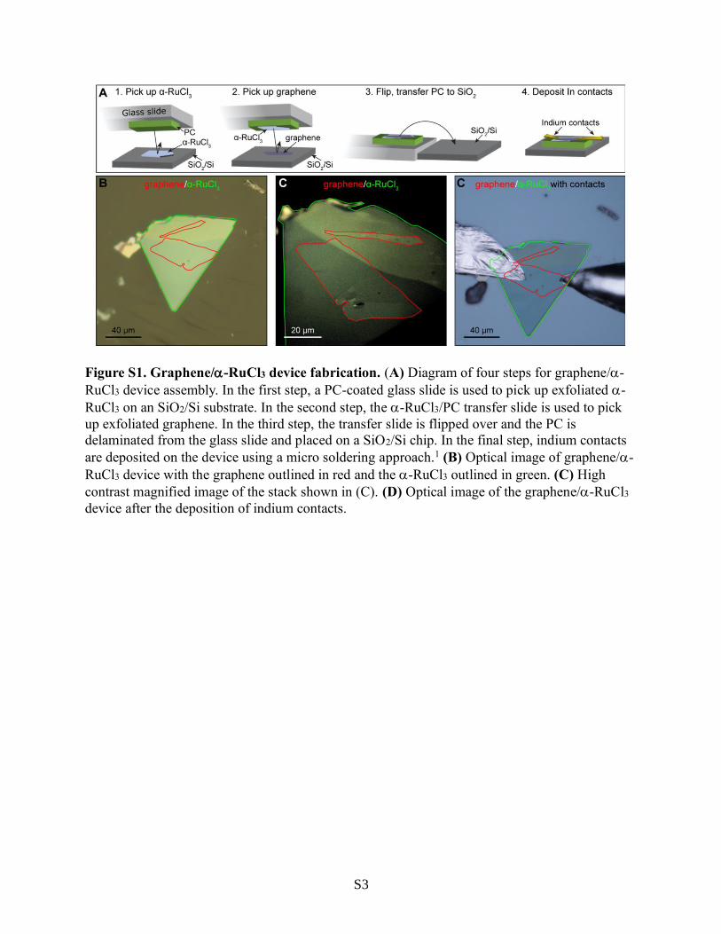
Figure S1. Graphene/-RuCl3 device fabrication. (A) Diagram of four steps for graphene/-
RuCl3 device assembly. In the first step, a PC-coated glass slide is used to pick up exfoliated -
RuCl3 on an SiO2/Si substrate. In the second step, the -RuCl3/PC transfer slide is used to pick
up exfoliated graphene. In the third step, the transfer slide is flipped over and the PC is
delaminated from the glass slide and placed on a SiO2/Si chip. In the final step, indium contacts
are deposited on the device using a micro soldering approach.1 (B) Optical image of graphene/-
RuCl3 device with the graphene outlined in red and the -RuCl3 outlined in green. (C) High
contrast magnified image of the stack shown in (C). (D) Optical image of the graphene/-RuCl3
device after the deposition of indium contacts.
S4
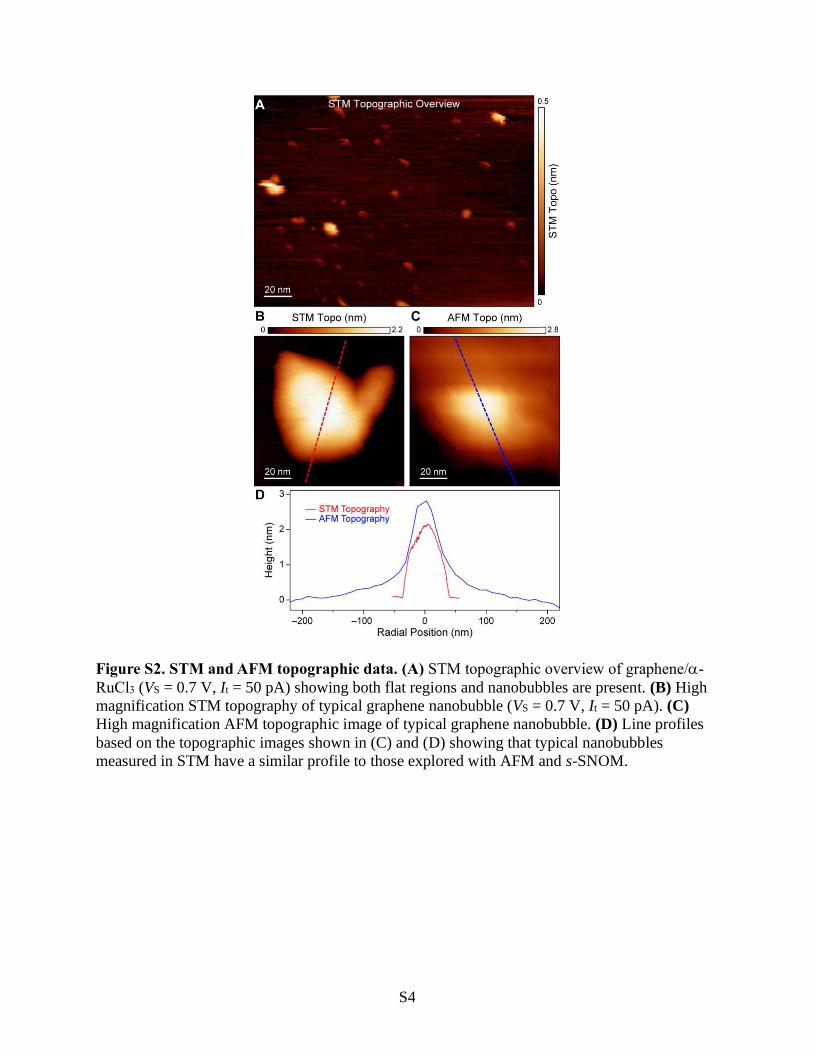
Figure S2. STM and AFM topographic data. (A) STM topographic overview of graphene/-
RuCl3 (VS = 0.7 V, It = 50 pA) showing both flat regions and nanobubbles are present. (B) High
magnification STM topography of typical graphene nanobubble (VS = 0.7 V, It = 50 pA). (C)
High magnification AFM topographic image of typical graphene nanobubble. (D) Line profiles
based on the topographic images shown in (C) and (D) showing that typical nanobubbles
measured in STM have a similar profile to those explored with AFM and s-SNOM.
S5
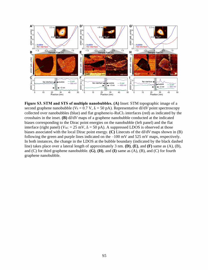
Figure S3. STM and STS of multiple nanobubbles. (A) Inset: STM topographic image of a
second graphene nanobubble (VS = 0.7 V, It = 50 pA). Representative dI/dV point spectroscopy
collected over nanobubbles (blue) and flat graphene/-RuCl3 interfaces (red) as indicated by the
crosshairs in the inset. (B) dI/dV maps of a graphene nanobubble conducted at the indicated
biases corresponding to the Dirac point energies on the nanobubble (left panel) and the flat
interface (right panel) (VAC = 25 mV, It = 50 pA). A suppressed LDOS is observed at those
biases associated with the local Dirac point energy. (C) Linecuts of the dI/dV maps shown in (B)
following the green and purple lines indicated on the –100 mV and 525 mV maps, respectively.
In both instances, the change in the LDOS at the bubble boundary (indicated by the black dashed
line) takes place over a lateral length of approximately 3 nm. (D), (E), and (F) same as (A), (B),
and (C) for third graphene nanobubble. (G), (H), and (I) same as (A), (B), and (C) for fourth
graphene nanobubble.

S6
Figure S4. s-SNOM on multiple nanobubbles with - and angle-dependent near-field
linecuts. (A) s-SNOM S3 amplitude (left panel) and 3 phase (right panel) collected over a
graphene nanobubble ( = 1170 cm–1). The black dashed lines separate the s-SNOM maps into
eight angular slices used for the analysis in (B). (B) The radial dependence of the s-SNOM S3
amplitude (red line) and 3 phase (blue line) integrated over the indicated angles designated in
(A). The lack of a systematic angular dependence suggests that p fringes do not contribute
significantly to the plasmonic response of nanobubbles. (C) The radial dependence of the S3
amplitude is shown for frequencies spanning = 930 cm–1 – 2280 cm–1 collected on bubble 2
(blue lines), bubble 4 (orange lines) and bubble 5 (purple lines) referenced in Fig. 3 of the main
manuscript. Since bubbles 1, 2, and 3 all overlap in frequency, only bubble 2 is shown for clarity.
All line profiles are truncated at the boundary of the associated nanobubble. (D) Same as (C) but
for the radial dependence of the 3 phase.
S7
Supplementary Discussion
Modeling near-field signal from plasmon reflection at a finite-sized bubble defect
As attested by our experimental results, we model the plasmonic response of a single
nanobubble in the graphene/-RuCl3 heterostructure by a local perturbation of the graphene sheet
conductivity 𝜎 with respect to its asymptotic value 𝜎(∞) arising from charge transfer from the -
RuCl3 underlayer. We denote the relative inhomogeneity in conductivity due the nanobubble as
𝜎(𝐫) = 𝜎(𝐫) 𝜎(∞)⁄ . To model the position-dependent near-field signal associated with reflections
of plasmon polaritons from the defect, we considered the integro-differential equation for the
scalar potential 𝜙𝑠 generated in response to the incident potential 𝜙probe of a near-field probe2:
[1 +
1
2𝜋𝑞𝑠𝑉 ∗ ∇ ⋅ 𝜎(𝐫) ∇] 𝜙(𝐫) = 𝜙probe(𝐫), 𝜙 = 𝜙probe + 𝜙𝑠 . (S1)
Here 𝑞𝑠 = 𝑖𝜔/(2𝜋𝜎(∞)) parameterizes the asymptotic conductivity away from the defect
through its associated plasmon polariton momentum, 𝑉(𝑟) = 1/(𝜅 𝑟) is the Coulomb kernel
screened by permittivity 휀 of the proximate -RuCl3 underlayer with 𝜅 = (휀 + 1)/2, and the
asterisk (∗) denotes the spatial convolution over the in-plane coordinate 𝐫 = (𝑥, 𝑦). As an
example, we choose 𝜎(𝐫) ≡ 1 + 𝛿Λ(𝑟/𝑅bubble), where 𝛿 is the characteristic magnitude of the
conductivity fluctuation at the nanobubble, 𝑅bubble is its width, and Λ(𝑟) = 1 − 𝜃(𝑟 − 1) is
taken as a step function of unit radius and height. We solved Eq. (S1) through expansion in an
orthonormal basis of plane waves 𝜙𝑗 = 𝐴𝑗𝑒𝑖𝐪𝑗⋅𝐫 periodic in a 2D square cell 𝑥, 𝑦 ∈[− 𝐿 2⁄ , 𝐿 2⁄ ], with 𝐴𝑗 a normalization constant and 𝐿 ≫ 𝑅bubble. If we assemble the Fourier
momenta 𝐪𝑗 and the Fourier coefficients �̃�𝑗 = ⟨𝜙𝑗|𝜙⟩ ≡ ∫ 𝜙𝑗∗(𝐫)𝜙(𝐫)𝑑2𝑟 into column vectors �⃗�
and �⃗⃗�, respectively, then ⟨𝜙𝑖|𝑉 ∗ |𝜙𝑗⟩ = 2𝜋/(𝜅 𝑞𝑖) 𝛿𝑖𝑗 with 𝛿𝑖𝑗 the Kronecker delta, and these
vectors must obey the equation
�⃗⃗� = [𝑞𝑠
∗ − (𝛿𝑄 + diag |�⃗�|)]−1
𝑞𝑠∗ �⃗⃗�probe , (S2)
where 𝑞𝑠∗ = 𝜅 𝑞𝑠 defines the screened polariton momentum, and 𝑄 is the scattering matrix with
the elements
𝑄𝑖𝑗 = (�̂�𝑖 ⋅ 𝐪𝑗) ⟨𝜙𝑖 |𝛬 (
𝑟
𝑅bubble)| 𝜙𝑗⟩ . (S3)
We defined another matrix-valued function 𝐺 by �⃗⃗�𝑠 = 𝐺 �⃗⃗�probe. From Eq. (S2), we obtain
𝐺𝑖𝑗 = ⟨𝜙𝑖|[𝑞𝑠
∗ − (𝛿𝑄 + diag |�⃗�|)]−1
(𝛿𝑄 + diag |�⃗�|)|𝜙𝑗⟩. (S4)
For a translationally invariant system, 𝛿 = 0, where the momentum is conserved, only the
diagonal matrix elements are nonzero. They can be understood as “in-plane” reflection
coefficients, and are related to the conventional Fresnel coefficients 𝑟𝑃(𝜔, 𝑞) by −𝐺𝑗𝑗 =
S8
𝑟𝑃(𝜔, 𝑞 = |𝐪𝑗|). Therefore, Im (−𝐺𝑗𝑗) = 𝑓(𝜔, 𝐪𝑗) has maxima at the same plasmon polariton
momenta |𝐪𝑗| = Re 𝑞𝑠∗ as Im 𝑟𝑃. However, our interest concerns 𝛿 ≠ 0.
Previous work3 has established a leading order approximation to the complex-valued
near-field signal 𝜌 scattered by a probe, given by the Fourier integral:
𝜌 ~ −1
2𝜋∫ 𝑑2𝑞 |𝐪| �̃�probe(𝐪) �̃�𝑠(𝐪) (S5)
where �̃�probe and �̃�s denote Fourier transforms of the respective potentials with respect to in-
plane (vector) momenta 𝐪 evaluated at the surface plane of the sample. The notation 𝜌 used here
for the near-field signal affirms its connection to the so-called photonic density of states as
motivated in ref. 3. In our case where 𝐪𝑗 describe a uniformly spaced grid of momenta spanning
the “first Brillouin zone” of the simulation domain, Eq. (S5) is readily evaluated by:
𝜌 ~1
2𝜋�⃗⃗�probe
𝑇 diag |�⃗�| 𝐺(𝑞𝑠∗, 𝑅bubble) �⃗⃗�probe. (S6)
Here we highlight that the dependence on screened plasmon wavevector and nanobubble size
resides in 𝐺(𝑞𝑠∗, 𝑅bubble), which encodes the associated inhomogeneous optical response.
We developed a Python-language computer code implementing the above equations taking
advantage of public-domain libraries and we used it to carry out a series of numerical simulations.
For simplicity, we approximated 𝜙probe(𝐫) by a potential of a point dipole placed a small distance
𝑧probe away from graphene4. Given an in-plane probe position 𝐫probe, the relative strength 𝛿 of
the perturbation due to the nanobubble, and the nanobubble radius 𝑅bubble, the code computes the
complex-valued amplitude and phase of 𝜌. We take 𝑧probe ≈ 𝑎 ≈ 30 nm to appropriately treat the
incident field from the near-field probe with apex radius 𝑎. Informed by our STS results
demonstrating near uniform suppression (on the scale of both 𝑎 and the unperturbed polariton
wavelength) of the graphene Fermi level to near the Dirac point across the entire nanobubble, we
take 𝛿 ≈ −1 to denote complete suppression of free carrier conductivity. Meanwhile, as a
representative case, we select 𝑅bubble = 30 nm ≈ 𝑎. Results presented in Fig. 3B of the main text
were obtained by computing 𝜌 for numerous values of 𝑞𝑠∗ and the probe position 𝑟 ≡ |𝐫probe|, and
normalizing the result by its value at 𝜌(𝑟 → ∞), thus highlighting contrasts due solely to the
nanobubble-scattered field. The result can be straightforwardly understood as uniquely a function
of three dimensionless ratios, 𝑧probe/𝑅bubble, 𝜆𝑝/𝑅bubble, and 𝑟/𝑅bubble, where 𝜆𝑝 ≡ 2𝜋/𝑞𝑠∗
defines the wavelength of the plasmon polariton in the bulk of graphene. The select results shown
in Fig. 3B of the main text are broadly characteristic of the case where 𝑧probe ∼ 𝑅bubble, and are
therefore well representative of the infrared nano-imaging results for nanobubbles characterized
in this work.
Derivation of scattering amplitude for plasmonic point-scatterer
In this section we utilize notations common to the previous section, where possible. The
polariton scattering problem Eq. (S1) admits an analytic solution for the total field 𝜙 = 𝜙probe +
𝜙𝑠 in the case that the excitation field 𝜙probe and the “defect” in graphene optical conductivity

S9
Δ𝜎(𝐫) = 𝜎(𝐫) − 1 take the form of a point source and a point scatterer, respectively. Provided
that the defect and source are “not too strong”, a perturbation theory can be applied. The
condition for its self-consistency will be discussed in context of the result. In this case, it is
convenient to rewrite Eq. (S1) in an operator notation:
[1 − (�̂�0 + 𝜖 ⋅ �̂�′)]𝜙 = 𝜙probe
where �̂�0 ≡ −1
2𝜋𝑞𝑠𝑉 ∗ ∇2 and �̂�′ ≡ −
1
2𝜋𝑞𝑠𝑉 ∗ ∇ ⋅
1
𝜖 𝛬(𝐫 − 𝐫0)∇.
(S7)
Here 𝛬(𝐫) ≈ 𝐴𝑠 𝛿(𝐫) denotes the profile selected to describe the defect centered at lateral
coordinate 𝐫0, with 𝐴𝑠 its integral weight, in units of area, and 𝛿(𝐫) a Dirac delta function.
Meanwhile, taking 𝜖 ≪ 1 supplies a perturbation expansion provided that �̂�′𝜙probe remains
“small”:
𝜙 = [1 − (�̂�0 + 𝜖 ⋅ �̂�′)]−1
𝜙probe
≈ [�̂�0 + 𝜖�̂�0�̂�′�̂�0 + 𝑂(𝜖2)]𝜙probe,
with �̂�0 ≡ (1 − �̂�0)−1
.
(S8)
Here �̂�0 defines a “bare” propagator for plasmon polaritons. This propagator can be obtained
through a Fourier representation of Eq. (S7) with respect to the in-plane wavevector 𝐪, whereby:
𝜙(𝐫) = ∫𝑑2𝑞
2𝜋𝑒𝑖𝒒⋅𝒓𝜙(𝐪), 𝜙(𝐫) = ∫
𝑑2𝑞
2𝜋𝑒𝑖𝒒⋅𝒓𝜙(𝐪), and �̂�0 = |𝐪|/𝑞𝑠
∗. (S9)
Here we use the unitary Fourier transform. In the Fourier domain, the propagator is naively then
expressed by 𝐺0(𝑞) = 𝑞𝑠∗/(𝑞𝑠
∗ − 𝑞). However, note that this form of the propagator �̂�0𝜙probe
can only generate the inhomogeneous part of solutions 𝜙, to which any arbitrary homogeneous
part 𝜙ℎ for which (1 − �̂�0)𝜙ℎ = 0 can also be added, e.g. 𝜙 = �̂�0𝜙probe + 𝜙ℎ, however
necessary to satisfy the prescribed boundary conditions. For the case of an open system of
graphene on -RuCl3 illuminated by a localized probe, we will demand an outgoing radiation
condition for 𝜙. In other words, 𝜙 must vanish at infinite distance, and (polariton) waves must
propagate outwards, with complex phase decreasing uniformly with distance from the source.
To this end, we can augment the propagator as follows to enforce this condition. We first
consider a point source placed at the origin, 𝜙probe(𝐫) = 𝐴𝑝𝛿(𝐫), where 𝐴𝑝 denotes the integral
weight of the excitation (in units of area), for which 𝜙probe(𝑞) = 𝐴𝑝/2𝜋. The inhomogeneous
part of the solution is given by:
[�̂�0𝜙probe](𝒓) =𝐴𝑝
2𝜋∫
𝑑2𝑞
2𝜋𝑒𝑖𝒒⋅𝒓𝐺(𝑞)
=𝐴𝑝
(2𝜋)2∫ 𝑑𝑞
∞
0
𝑞 (𝑞𝑠
∗
𝑞𝑠∗ − 𝑞
) ∫ 𝑑𝜃2𝜋
0
𝑒𝑖𝑞𝑟 cos 𝜃
S10
= −𝐴𝑝𝑞𝑠
∗
2𝜋∫ 𝑑𝑞
∞
0
𝑞
𝑞 − 𝑞𝑠∗
𝐽0(𝑞𝑟)
= −𝐴𝑝𝑞𝑠
∗2
2𝜋[
1
𝑞𝑠∗𝑟
−𝜋
2(𝑌0(𝑞𝑠
∗𝑟) + 𝐇0(𝑞𝑠∗𝑟))]
(S10)
Here we have applied identity (2.12.3.11) of ref. 5 to the case of the Bessel function of order 𝜈 =0, where 𝐽0(… ), 𝑌0(… ) and 𝐇0(… ) denote Bessel functions of the first and second kinds and the
Struve-H function, respectively, all of order 𝜈 = 0. For distances 𝑟0 ≫ 𝜆𝑝 = 2𝜋/𝑅𝑒[𝑞𝑠∗], the
sum in brackets is very nearly equal to −𝜋 𝑌0(𝑞𝑠∗𝑟), which can be identified as the
inhomogeneous part of the solution to the wave equation with open boundary conditions. The
outgoing wave condition is therefore enforceable by an added homogeneous part 𝜙ℎ ∝𝑖𝜋 𝐽0(𝑞𝑠
∗𝑟), in which case the term in square brackets becomes very nearly equal to 𝑖𝜋 𝐻01(𝑞𝑠
∗𝑟),
with 𝐻01(… ) the Hankel function of the first kind of order 𝜈 = 0, representing an outgoing
cylindrical wave. Consequently, we forthwith augment the Fourier space propagator to enforce
our prescribed boundary conditions:
𝐺(𝑞) = 𝑞𝑠∗ (
1
𝑞𝑠∗ − 𝑞
+ 𝑖𝜋𝛿(𝑞 − 𝑞𝑠∗)),
so that 𝐺0(𝑟) ≈𝑖
2𝑞𝑠
∗2𝐻01(𝑞𝑠
∗𝑟).
(S11)
Here the Dirac delta function supplies the homogeneous component in Fourier space. Deviations
not captured by this functional form at distances 𝑟 → 0 associate with the “local” metallic
response of the plasmonic medium, which supply screening of the incident divergent field as
𝑞𝑠∗ → 0 in the limit where surface conductivity diverges to infinity. While this physical behavior
is not captured by a mere wave solution, it remains inessential to our experimental results.
Meanwhile, the Fourier space representation for �̂�′ operating on a function 𝑓(𝐪) is:
[�̂�′𝑓](𝐪) =1
𝜖𝑞𝑠∗
�̂� ⋅ ∫ 𝑑2𝑞′ 2𝜋 𝛬(𝐪 − 𝐪′) 𝐪′ 𝑓(𝐪′) (S12)
Here �̂� denotes a unit wavevector, and real-space multiplication by 𝛬(𝐫 − 𝐫0) within �̂�′ is
transformed by the convolution theorem into an integral kernel 2𝜋 𝛬(𝐪 − 𝐪′). Next, we apply
the Fourier representation of the defect profile 𝛬(𝑞) = 𝑒−𝑖𝐪⋅𝐫0/2𝜋 representing the Dirac delta
function centered at 𝐫0, obtaining:
[�̂�′𝑓](𝐪) =𝐴𝑠
𝜖𝑞𝑠∗
�̂� ⋅ ∫ 𝑑2𝑞′ 𝑒−𝑖(𝐪−𝐪′)⋅𝐫0 𝐪′ 𝑓(𝑞′)
=𝐴𝑠
𝜖𝑞𝑠∗
𝑒−𝑖𝐪⋅𝐫0 ∫ 𝑑𝑞′∞
0
𝑞′2𝑓(𝑞′) ∫ 𝑑𝜃′2𝜋
0
cos(𝜃′ − 𝜃) 𝑒𝑖𝑞′𝑟0 cos 𝜃′
=2𝜋𝑖 𝐴𝑠
𝜖𝑞𝑠∗
cos 𝜃 𝑒−𝑖𝑞𝑟0 cos 𝜃 ∫ 𝑑𝑞′∞
0
𝑞′2 𝐽1(𝑞′𝑟0) 𝑓(𝑞′).
(S13)

S11
Here 𝐽1 denotes the Bessel function of the first kind of order 𝜈 = 1, and 𝜃′ and 𝜃 denote the
angles subtended between the position vector 𝐫0 and the incoming and outgoing wavevectors 𝐪′
and 𝐪, respectively. Here we have also assumed 𝑓(𝐪) to be an isotropic function. Since the
defect-scattered field is given by Δ𝜙(𝐫) = 𝜖�̂�0�̂�′�̂�0 𝜙probe(𝐫), then 𝑓 = �̂�0 𝜙probe, and our
point source at the origin is compatible with this assumption. The latter integral in Eq. (S13) can
now be evaluated:
𝑓(𝑞) = [�̂�0 𝜙probe](𝑞) = 𝑞𝑠∗ (
1
𝑞𝑠∗ − 𝑞
+ 𝑖𝜋𝛿(𝑞 − 𝑞𝑠∗))
𝐴𝑝
2𝜋, so that
∫ 𝑑𝑞′∞
0
𝑞′2 𝐽1(𝑞′𝑟0) 𝑓(𝑞′) =𝐴𝑝𝑞𝑠
∗
2𝜋[𝑖𝜋𝑞𝑠
∗2 𝐽1(𝑞𝑠∗𝑟0) + ∫ 𝑑𝑞′
∞
0
𝑞′2
𝑞𝑠∗ − 𝑞′
𝐽1(𝑞′𝑟0)]
=𝐴𝑝𝑞𝑠
∗
2𝜋[𝑖𝜋 𝐽1(𝑞𝑠
∗𝑟0) −𝜕
𝜕𝑟0∫ 𝑑𝑞′
∞
0
𝑞′
𝑞𝑠∗ − 𝑞′
𝐽0(𝑞′𝑟0)]
=𝐴𝑝𝑞𝑠
∗2
2𝜋{𝑖𝜋𝑞𝑠
∗ 𝐽1(𝑞𝑠∗𝑟0) −
𝜕
𝜕𝑟0[
1
𝑞𝑠∗𝑟
−𝜋
2(𝑌0(𝑞𝑠
∗𝑟) + 𝐇0(𝑞𝑠∗𝑟))]}.
(S14)
Noting again that the sum in square brackets is very approximately equal to −𝜋𝜕𝑟0𝑌0(𝑞𝑠
∗𝑟) =
+𝜋𝑞𝑠∗𝑌1(𝑞𝑠
∗𝑟), the sum in curled brackets is also very nearly equal to 𝑖𝜋𝑞𝑠∗ 𝐻1
1(𝑞𝑠∗𝑟0), a Hankel
function of the first kind of order 𝜈 = 1. Inserting this wave function back into Eq. (13), we
have:
[�̂�′�̂�0 𝜙probe](𝐪) = (2𝜋𝑖 𝐴𝑠
𝜖𝑞𝑠∗
cos 𝜃 𝑒−𝑖𝑞𝑟0 cos 𝜃) ×𝐴𝑝𝑞𝑠
∗2
2𝜋× 𝑖𝜋𝑞𝑠
∗ 𝐻11(𝑞𝑠
∗𝑟0)
= −𝑖𝜋
𝜖𝐴𝑠𝐴𝑝𝑞𝑠
∗2𝐻11(𝑞𝑠
∗𝑟0) cos 𝜃 𝑒−𝑖𝑞𝑟0 cos 𝜃
(S15)
The field scattered by the defect can now be evaluated at the origin 𝐫 = 𝟎, coinciding with the
location of the probe field, as:
Δ𝜙(𝐫 = 𝟎) = 𝜖 ∫𝑑2𝑞
2𝜋 [�̂�0�̂�′�̂�0 𝜙probe](𝐪)
= −𝑖𝜋𝐴𝑠𝐴𝑝𝑞𝑠∗3𝐻1
1(𝑞𝑠∗𝑟0) ∫ 𝑑𝑞 𝑞
∞
0
(1
𝑞𝑠∗ − 𝑞
+ 𝑖𝜋𝛿(𝑞 − 𝑞𝑠∗)) ∫
𝑑𝜃
2𝜋
2𝜋
0
cos 𝜃 𝑒−𝑖𝑞𝑟0 cos 𝜃
= +𝑖𝜋𝐴𝑠𝐴𝑝𝑞𝑠∗3𝐻1
1(𝑞𝑠∗𝑟0) [𝑖𝜋𝑞𝑠
∗ 𝐽1(𝑞𝑠∗𝑟0) + ∫ 𝑑𝑞
∞
0
𝑞
𝑞𝑠∗ − 𝑞
𝐽1(𝑞𝑟0)]
≈ 𝑖𝜋𝐴𝑠𝐴𝑝𝑞𝑠∗3𝐻1
1(𝑞𝑠∗𝑟0) × −
𝜕
𝜕𝑟0𝑖𝜋 𝐻0
1(𝑞𝑠∗𝑟)
≈ −(𝐴𝑠𝑞𝑠∗2)(𝐴𝑝𝑞𝑠
∗2) (𝜋𝐻11(𝑞𝑠
∗𝑟0))2
.
(S16)
(S17)

S12
Here we have identified the term in square brackets as proportional to the 𝑟0-derivative of our
augmented propagator 𝐺0(𝑟 = 𝑟0), for which we readily supply the outgoing wave
approximation (Eq (11)).
We note that the two leading dimensionless terms in parentheses in Eq. (S17) scale as the
perturbation area in comparison to the plasmon wavelength 𝜆𝑝 = 2𝜋/𝑞𝑠∗ squared. In the context
where graphene nanobubbles scatter plasmon polariton fields with momentum 𝑞𝑠∗, the defect area
is described by 𝐴𝑠 = −𝜋𝑅bubble2 (negation implying a deficit of conductivity) and the
perturbation treatment applied here is self-consistent so long as 𝑅bubble ≪ 𝜆𝑝. Since excitation
from the near-field probe may be described by 𝐴𝑝~𝑎2 with 𝑎 the probe tip radius, the condition
𝑎 < 𝜆𝑝 implies the perturbation treatment here should be a particularly robust description of our
experiments. Our nano-imaging experiments approximately detect the vertically polarized field
scattered on the graphene surface. This field is proportional to instantaneous surface charge on
the graphene, which is in turn proportional to Δ𝜙(𝐫). Taking 𝑟0 as the probe-nanobubble
separation distance, we can therefore directly apply the complex-valued functional form
𝐻11(𝑞𝑠
∗𝑟0)2 to fit the line-profiles presented in Fig. 3C of the main text. This form is
characterized by alternating fringes with an apparent spatial period of 𝜆𝑝/2, owing to round-trip
traversal of polariton fields over a cumulative distance 2𝑟0 between the probe and the
nanobubble and back. This formalism therefore supplies a quantitative means to extract plasmon
polariton momentum and wavelength directly from our nano-infrared images.
S13
References
[1] Girit, Ç. Ö. & Zettl, A. Soldering to a single atomic layer. Applied Physics Letters 91,
193512, (2007).
[2] Rejaei, B. & Khavasi, A. Scattering of surface plasmons on graphene by a discontinuity
in surface conductivity. Journal of Optics 17, 075002, (2015).
[3] Jing, R., Shao, Y., Fei, Z., Lo, C. F. B., Vitalone, R. A., Ruta, F. L., Staunton, J., Zheng,
W. J. C., McLeod, A. S., Sun, Z., Jiang, B.-y., Chen, X., Fogler, M. M., Millis, A. J., Liu,
M., Cobden, D. H., Xu, X. & Basov, D. N. Terahertz response of monolayer and few-
layer WTe2 at the nanoscale. Nature Communications 12, 5594, (2021).
[4] Nikitin, A., Alonso-González, P., Vélez, S., Mastel, S., Centeno, A., Pesquera, A.,
Zurutuza, A., Casanova, F., Hueso, L. & Koppens, F. Real-space mapping of tailored
sheet and edge plasmons in graphene nanoresonators. Nature Photonics 10, 239-243,
(2016).
[5] Prudnikov, A. P., Brychkov, I. U. A. & Marichev, O. I. Integrals and series: special
functions. Vol. 2 (CRC press, 1986).