Embed Size (px)
Citation preview
1 Nano materials for Eng. chemistry students of (B.E) prescribed by VTU Prepared by - M.PRAVEEN, DEPT OF CHEMISTRY Dr SMCE, BANGALORE.
For any queries and doubts free feel to mail me at: [email protected]
Nano materials
1). Introduction: Nanomaterials describe, in principle, materials of which a single unit
is sized (in at least one dimension) between 1 and 1000 nanometers (10−9 meter) but is usually
1—100 nm (the usual definition of nanoscale).
Nanotechnology – study of physical phenomena on the nanoscale, dealing with things measured
in nanometres, billionths of a meter. Nanotechnology is a complex scientific area involving the
rearrangement of atoms at a molecular level, i.e. creating devices at a molecular level. Atomic
rearrangement depends on the material used because any alteration of the atoms changes the
identity of the material. Nanotechnology is rearranging atoms to create things at an extremely
small scale, and it was popularized by Eric Drexler: "Eric Drexler was the godfather of
nanotechnology." In 1977, Drexler had the idea of creating tiny robots that were able to
manipulate molecules and produce any substance in a very small amount of time. He was the
spark that started nanotechnology research. Nanotechnology has come a long way from 1977 to
today.
Nanomaterials research takes a materials science-based approach to nanotechnology, leveraging
advances in materials metrology and synthesis which have been developed in support of
microfabrication research. Materials with structure at the nanoscale often have unique optical,
electronic, or mechanical properties.
Natural nanomaterials:
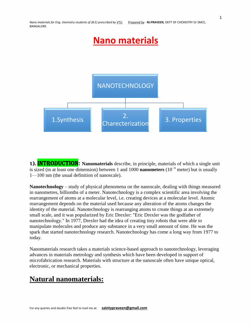
NANOTECHNOLOGY
1.Synthesis2.
Charecterization3. Properties

2 Nano materials for Eng. chemistry students of (B.E) prescribed by VTU Prepared by - M.PRAVEEN, DEPT OF CHEMISTRY Dr SMCE, BANGALORE.
For any queries and doubts free feel to mail me at: [email protected]
Biological systems often feature natural, functional nanomaterials. The structure of foraminifera
and viruses (capsid), the wax crystals covering a lotus or nasturtium leaf, spider and spider-mite
silk the "spatulae" on the bottom of gecko feet, some butterfly wing scales, natural colloids
(milk, blood), horny materials (skin, claws, beaks, feathers, horns, hair), paper, cotton, nacre,
corals, and even our own bone matrix are all natural organic nanomaterials.
Natural inorganic nanomaterials occur through crystal growth in the diverse chemical conditions
of the earths crust. For example clays display complex nanostructures due to anisotropy of their
underlying crystal structure, and volcanic activity can give rise to opals, which are an instance of
a naturally occurring photonic crystals due to their nanoscale structure. Fires represent
particularly complex reactions and can produce pigments, cement, fumed silica etc.
Viral capsid Lotus effect gecko's foot butterfly wing
.
Crystal Opal Peacock feather Lycurgus Cup
Glass, 4th century, Roman. Nanoparticles (70 nm) of gold and silver, dispersed in colloidal form, are responsible for the dichroic effect (red/green).
1. Synthesis: bottom up approach AND top down approach
The field of nanomaterials is loosely organized, like the traditional field of chemistry, into organic
(carbon-based) nanomaterials such as fullerenes, and inorganic nanomaterials based on other elements,
such as silicon. See also Nanomaterials in List of nanotechnology topics
Synthesis

3 Nano materials for Eng. chemistry students of (B.E) prescribed by VTU Prepared by - M.PRAVEEN, DEPT OF CHEMISTRY Dr SMCE, BANGALORE.
For any queries and doubts free feel to mail me at: [email protected]
The goal of any synthetic method for nanomaterials is to yield a material that exhibits properties
that are a result of their characteristic length scale being in the nanometer range (~1 – 100 nm).
Accordingly, the synthetic method should exhibit control of size in this range so that one
property or another can be attained. Often the methods are divided into two main types "Bottom
Up" and "Top Down."
Bottom up methods
Bottom up methods involve the assembly of atoms or molecules into nanostructured arrays. In
these methods the raw material sources can be in the form of gases, liquids or solids. The latter
requiring some sort of disassembly prior to their incorporation onto a nanostructure. Bottom
methods generally fall into two categories: chaotic and controlled.
Chaotic processes
Chaotic processes involve elevating the constituent atoms or molecules to a chaotic state and
then suddenly changing the conditions so as to make that state unstable. Through the clever
manipulation of any number of parameters, products form largely as a result of the insuring
kinetics. The collapse from the chaotic state can be difficult or impossible to control and so
ensemble statistics often govern the resulting size distribution and average size. Accordingly,
control of nanoparticle formation is controlled through manipulation of the end state of the
products.
Examples of Chaotic Processes are: Laser ablation, Exploding wire, Arc, Flame pyrolysis,
Combustion, Precipitation synthesis techniques.
Controlled processes
Controlled Processes involve the controlled delivery of the constituent atoms or molecules to the
site(s) of nanoparticle formation such that the nanoparticle can grow to a prescribed sizes in a
controlled manner. Generally the state of the constituent atoms or molecules are never far from
that needed for nanoparticle formation. Accordingly, nanoparticle formation is controlled
through the control of the state of the reactants.
Examples of Controlled Processes are, Self-limiting growth solution, Self-limiting chemical
vapor precipitation and Shaped pulse femtosecond laser techniques, Molecular beam epitaxy.
Top down methods
Knowledge of processes for bottom-up assembly of structures remain in their infancy in
comparison to traditional manufacturing techniques. As a result, the most mature products of
nanotechnology (such as modern CPUs) rely heavily on top-down processes to define structures.
The traditional example of a top-down technique for fabrication is lithography in which
instruments (such as a modern stepper) are used to scale a macroscopic plan to the nanoscale.

4 Nano materials for Eng. chemistry students of (B.E) prescribed by VTU Prepared by - M.PRAVEEN, DEPT OF CHEMISTRY Dr SMCE, BANGALORE.
For any queries and doubts free feel to mail me at: [email protected]
4). Sol gel:
In materials science, the sol-gel process is a method for producing solid materials from small
molecules. The method is used for the fabrication of metal oxides, especially the oxides of silicon
and titanium. The process involves conversion of monomers into a colloidal solution (sol) that acts
as the precursor for an integrated network (or gel) of either discrete particles or network polymers.
Typical precursors are metal alkoxides.
Afterwards, a thermal treatment, or firing process, is often necessary in order to favor further
polycondensation and enhance mechanical properties and structural stability via final sintering,
densification and grain growth. One of the distinct advantages of using this methodology as opposed
to the more traditional processing techniques is that densification is often achieved at a much lower
temperature.
The precursor sol can be either deposited on a substrate to form a film (e.g., by dip coating or spin
coating), cast into a suitable container with the desired shape (e.g., to obtain
monolithic ceramics, glasses, fibers, membranes, aerogels), or used to synthesize powders
(e.g., microspheres, nanospheres). The sol-gel approach is a cheap and low-temperature technique
that allows for the fine control of the product’s chemical composition. Even small quantities of
dopants, such as organic dyes and rare earth elements, can be introduced in the sol and end up
uniformly dispersed in the final product. It can be used in ceramics processing and manufacturing as
an investment casting material, or as a means of producing very thin films of metal oxides for various
purposes. Sol-gel derived materials have diverse applications in optics, electronics, energy, space,
5 Nano materials for Eng. chemistry students of (B.E) prescribed by VTU Prepared by - M.PRAVEEN, DEPT OF CHEMISTRY Dr SMCE, BANGALORE.
For any queries and doubts free feel to mail me at: [email protected]
(bio)sensors, medicine (e.g., controlled drug release), reactive material and separation
(e.g., chromatography) technology.
The interest in sol-gel processing can be traced back in the mid-1800s with the observation that the
hydrolysis of tetraethyl orthosilicate (TEOS) under acidic conditions led to the formation of SiO2 in
the form of fibers and monoliths. Sol-gel research grew to be so important that in the 1990s more
than 35,000 papers were published worldwide on the process.
Removal of the remaining liquid (solvent) phase requires a drying process, which is typically
accompanied by a significant amount of shrinkage and densification. The rate at which the solvent
can be removed is ultimately determined by the distribution of porosity in the gel. The
ultimate microstructure of the final component will clearly be strongly influenced by changes imposed
upon the structural template during this phase of processing.
5).Precipitation:
(CPT) or co-precipitation is the carrying down by a precipitate of substances normally
soluble under the conditions employed. Analogously, inmedicine, coprecipitation is specifically the
precipitation of an unbound "antigen along with an antigen-antibody complex".
Coprecipitation is an important issue in chemical analysis, where it is often undesirable, but in some
cases it can be exploited. In gravimetric analysis, which consists on precipitating the analyte and
measuring its mass to determine its concentration or purity, coprecipitation is a problem because
undesired impurities often coprecipitate with the analyte, resulting in excess mass. This problem can
often be mitigated by "digestion" (waiting for the precipitate to equilibrate and form larger, purer
particles) or by redissolving the sample and precipitating it again.

6 Nano materials for Eng. chemistry students of (B.E) prescribed by VTU Prepared by - M.PRAVEEN, DEPT OF CHEMISTRY Dr SMCE, BANGALORE.
For any queries and doubts free feel to mail me at: [email protected]
There are three main mechanisms of coprecipitation: inclusion, occlusion, and
adsorption.[3] An inclusion occurs when the impurity occupies a lattice site in the crystal structure of
the carrier, resulting in a crystallographic defect; this can happen when the ionic radius and charge
of the impurity are similar to those of the carrier. An adsorbate is an impurity that is weakly bound
(adsorbed) to the surface of the precipitate. An occlusion occurs when an adsorbed impurity gets
physically trapped inside the crystal as it grows.
Besides its applications in chemical analysis and in radiochemistry, coprecipitation is also
"potentially important to many environmental issues closely related to water resources, including
acid mine drainage, radionuclide migration in fouled waste repositories, metal contaminant transport
at industrial and defense sites, metal concentrations in aquatic systems, and wastewater treatment
technology".[4]
Coprecipitation is also used as a method of magnetic nanoparticle synthesis.[5]
7 Nano materials for Eng. chemistry students of (B.E) prescribed by VTU Prepared by - M.PRAVEEN, DEPT OF CHEMISTRY Dr SMCE, BANGALORE.
For any queries and doubts free feel to mail me at: [email protected]
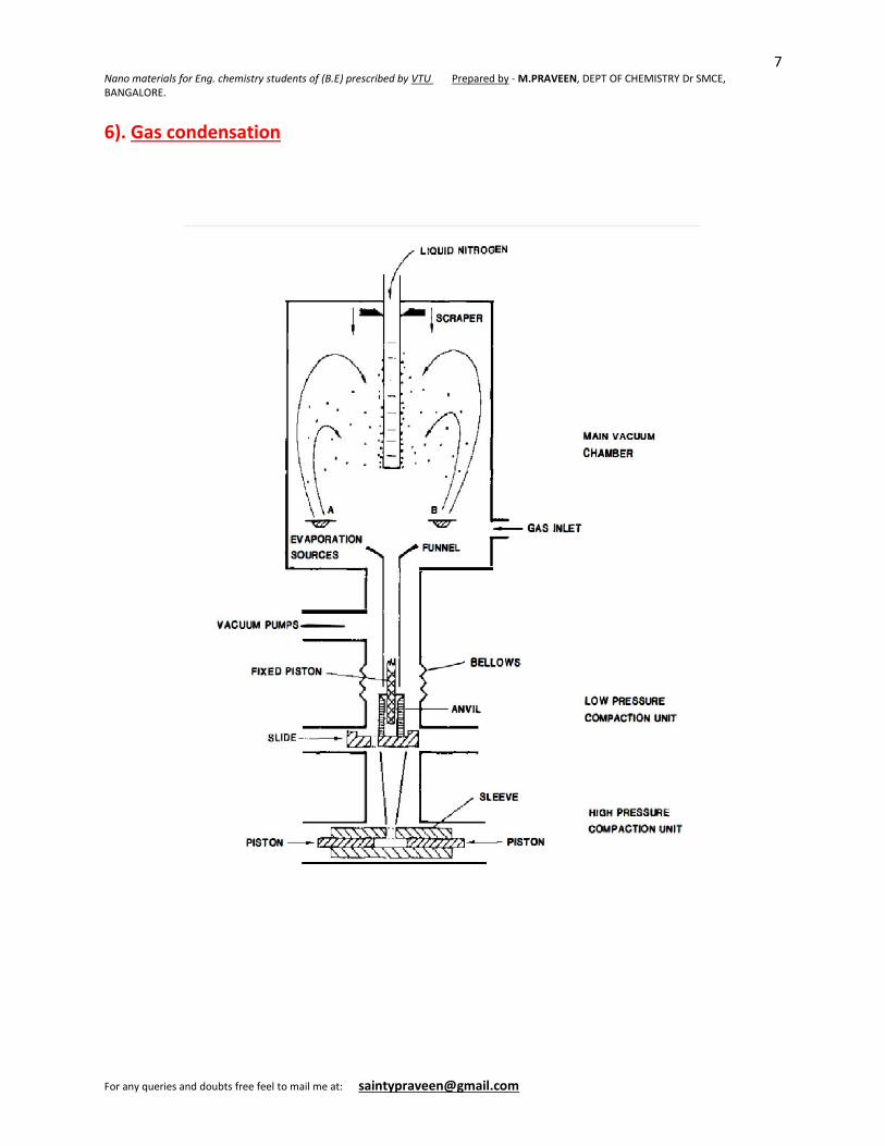
6). Gas condensation

8 Nano materials for Eng. chemistry students of (B.E) prescribed by VTU Prepared by - M.PRAVEEN, DEPT OF CHEMISTRY Dr SMCE, BANGALORE.
For any queries and doubts free feel to mail me at: [email protected]
7).CVD:
Chemical vapor deposition (CVD) is a chemical process used to produce high quality, high-
performance, solid materials. The process is often used in the semiconductor industry to
produce thin films. In typical CVD, the wafer (substrate) is exposed to one or more volatile
precursors, which react and/or decompose on the substrate surface to produce the desired deposit.
Frequently, volatile by-products are also produced, which are removed by gas flow through the
reaction chamber.
Microfabrication processes widely use CVD to deposit materials in various forms,
including: monocrystalline, polycrystalline, amorphous, and epitaxial. These materials
include: silicon, carbon fiber, carbon nanofibers, fluorocarbons, filaments, carbon
nanotubes, SiO2, silicon-germanium, tungsten, silicon carbide, silicon nitride, silicon
oxynitride, titanium nitride, and various high-k dielectrics. CVD is also used to produce synthetic
diamonds.
Uses
CVD is commonly used to deposit conformal films and augment substrate surfaces in ways that
more traditional surface modification techniques are not capable of. CVD is extremely useful in the
process of atomic layer deposition at depositing extremely thin layers of material. A variety of
applications for such films exist. Gallium arsenide is used in some integrated circuits (ICs) and
photovoltaic devices. Amorphous polysilicon is used in photovoltaic devices.
Certain carbides and nitrides confer wear-resistance.[7]Polymerization by CVD, perhaps the most
versatile of all applications, allows for super-thin coatings which possess some very desirable
qualities, such as lubricity, hydrophobicity and weather-resistance to name a few.

9 Nano materials for Eng. chemistry students of (B.E) prescribed by VTU Prepared by - M.PRAVEEN, DEPT OF CHEMISTRY Dr SMCE, BANGALORE.
For any queries and doubts free feel to mail me at: [email protected]
8). Hydrothermal :
hydrothermal synthesis — a method to produce different chemical compounds and
materials using closed-system physical and chemical processes flowing in aqueous solutions
at temperatures above 100°C and pressures above 1 atm
The method is based on the ability of water and aqueous solutions to dilute at high temperature
(500°C) and pressure (10-80 MPa, sometimes up to 300 MPa) substances practically insoluble under
normal conditions: some oxides, silicates, sulphides. The main parameters of hydrothermal synthesis,
which define both the processes kinetics and the properties of resulting products, are the initial pH of
the medium, the duration and temperature of synthesis, and the pressure in the system. The
synthesis is carried out in autoclaves which are sealed steel cylinders that can withstand high
temperatures and pressure for a longtime.
Nanopowders are normally produced by means of either high temperature hydrolysis reactions of
various compounds directly in the autoclave or hydrothermal treatment of reaction products at room
temperature; the latter case is based on the sharp increase in the rate of crystallisation of many
amorphous phases in hydrothermal conditions. In the first case the autoclave is loaded with aqueous
solution of precursor salts, in the second case – with suspension of products derived from solution
reactions flowing under normal conditions. There is normally no need to use special equipment and
maintain a temperature gradient.
Advantages of the hydrothermal synthesis method include the ability to synthesise crystals of
substances which are unstable near the melting point, and the ability to synthesise large crystals of
high quality. Disadvantages are the high cost of equipment and the inability to monitor crystals in the
process of their growth. Hydrothermal synthesis can be effected both under temperatures and
pressures below the critical point for a specific solvent above which differences between liquid and
vapour disappear, and under supercritical conditions. The solubility of many oxides in hydrothermal
solutions of salts is much higher than in pure water; such salts are called mineralizers. There is also a
group of solvothermal synthesis methods, relational to hydrothermal methods; this group of methods
is based on the use of organic solvents and supercritical CO2.
Substantial enhancement of the hydrothermal method facilitates the use of additional external factors
to control the reaction medium during the synthesis process. As of now, this approach is implemented
in the hydrothermal-microwave, hydrothermal-ultrasonic, hydrothermal-electrochemical and
hydrothermal-mechanochemical synthesis methods.
One of the most widely known nanomaterials produced by the hydrothermal method are
synthetic zeolites. A necessary condition for their production is the presence in the solution of some
surface active agents (SAA) that actively influence morphological evolution of oxide compounds in
hydrothermal solutions. The choice of synthesis conditions and type of surfactants can ensure the
production of targeted porous nanomaterials with given pore size controlled in a fairly wide range of
values.

10 Nano materials for Eng. chemistry students of (B.E) prescribed by VTU Prepared by - M.PRAVEEN, DEPT OF CHEMISTRY Dr SMCE, BANGALORE.
For any queries and doubts free feel to mail me at: [email protected]
Nanocrystalline TiO2 produced by the hydrothermal technique.
9). Thermolysis: heating to high temperature sometimes will yield to
agglomeration of atoms to bind and grow as a crystal. In other hand heating
a compound leads to cracking a compound, breaks into several tiny pieces,
particles of very low particle weight such as ash from furnaces
2. Characterization: (not in the syllabus for Chemistry
cycle)
UV- visible spectroscopy
XRD: X-ray diffraction technique
FTIR technique: Furrier transformation infrared
spectroscopy
RAMAN spectroscopy: utilizes monochromatic LASER light

11 Nano materials for Eng. chemistry students of (B.E) prescribed by VTU Prepared by - M.PRAVEEN, DEPT OF CHEMISTRY Dr SMCE, BANGALORE.
For any queries and doubts free feel to mail me at: [email protected]
Thin film analyzer:
Particle size analyzer:
AFM: atomic force microscope
SEM: scanning electron microscope
TEM: transmission electron microscopy
3. Properties: (size dependent)
Size-Dependent Properties At the nanometer scale property become size dependent. For example: 1. Mechanical properties-adhesion, capillary forces 2. Chemical Properties-reactivity, catalysis

12 Nano materials for Eng. chemistry students of (B.E) prescribed by VTU Prepared by - M.PRAVEEN, DEPT OF CHEMISTRY Dr SMCE, BANGALORE.
For any queries and doubts free feel to mail me at: [email protected]
3. Thermal Properties-melting point 4. Electrical properties-tunneling current 5. Optical properties-absorption, scattering 6. Magnetic properties- super paramagnetic effect New properties enable new applications!
Classes of Materials Composite Materials
Thermal Behavior: Heat affects mechanical, electrical, and optical properties .As temperature rises, materials expand, the elastic modulus decreases, the strength falls, and the material start to creep, deforming slowly until the melting point is reached. Electrical resistivity rises with temperature, the refractive index falls, and color may change.
Thermal Transport of Nanomaterials: Classical size effects. In bulk materials the characteristic length of the box is much longer than the mean free path. Therefore, the collisions between the molecules (electrons, phonons) and the wall are neglected and thermal conductivity is regarded as a bulk property. In nanomaterials the mean free path becomes comparable or larger than the size of the system.
Quantum size effects. According to quantum mechanics, electrons and phonons are also material waves. In the case of a bulk material the wavelength of phonons are much smaller than the length scale of the sample. However, in nanomaterials the length scale of the material is similar to the wavelength of the phonons. Therefore, quantum confinement occurs. In 0D nanomaterials (nanoparticles) confinement occurs in 3 dimensions In 1D nanomaterials (nanowires, and nanotubes) Confinement is restricted to 2 dimensions In 2D nanomaterials (nanofilms, nanocoatings) quantum confinement takes place in one dimension

13 Nano materials for Eng. chemistry students of (B.E) prescribed by VTU Prepared by - M.PRAVEEN, DEPT OF CHEMISTRY Dr SMCE, BANGALORE.
For any queries and doubts free feel to mail me at: [email protected]
Quantum size effects. The presence of the surface in nanostructures causes a change in the distribution of the phonon frequencies, and creates new modes that are not present in bulk. The same happens for electron. One-dimensional materials behave as phonon waveguide, similar to
optical one for light. For example for carbon nanotubes, several authors have predicted very high thermal
conductivity along the nanotube, close to 3000 Wm-1K-1. As a comparison we should keep in mind that
the thermal conductivity of copper is approximately 400 Wm-1K-1. Despite these results, there are still
open questions about phonon transport in 1D nanostructures, particularly regarding phonon/phonon
interactions and the role of defects.
Electrical Behavior: How come some materials have mobile electrons and some do not? To answer this question we need quantum mechanics the electrons of an atom occupy discrete energy levels. The electrons fills the shells with the lowest energy according to the Pauli principle (two electrons of opposite spin in each orbit).
Optical Behavior in Nanostructures The effect of nanoscale on optical absorption are associated with: 1. The density of states in valence and conduction bands 2. The quantized energy levels of the nanostructures 3. The influence of excitonic effects. When moving from 3D to 0D quantum confinement is more severe, band gap shift to higher energies, i.e. shorter wavelengths. A blue is expected whe the size is decreased and red when the size is increased. Optical Behavior in Nanostructures
Cd-Se quantum dots of various size Also emission of photons can be tuned with the nanoparticle size. Typical trend is a shift of the emission peak toward shorter wavelength (blshift).
10). Nano scale materials:
14 Nano materials for Eng. chemistry students of (B.E) prescribed by VTU Prepared by - M.PRAVEEN, DEPT OF CHEMISTRY Dr SMCE, BANGALORE.
For any queries and doubts free feel to mail me at: [email protected]
11). Nano crystals and clusters:
12). Nanocystaline materials:
13). Fullerenes
Carbon nanomaterials — a collective term denoting carbon-based small-scale
structures or nanostructured materials.
Description
Carbon nanomaterials include fullerenes (see also fullerite) and their derivatives (see also
fulleride, endohedral fullerene), carbon nanotubes, carbon nanofibers, nanodiamonds and
graphenes (see also graphane).
Carbon nanomaterials are often used as filling compounds in composites, the most widely known of
which are composite materials with a polymer matrix.
14). CNT
carbon nanotube(CNT); SWNT; MWNT— a hollow cylindrical structure with diameter
varying from fractions of a nanometer to several dozen nanometers and length ranging from
one micron to several hundred microns or more; carbon nanotube consists of carbon atoms
and is a rolled-up graphene sheet.
Description
Carbon nanotubes (CNT) were first systematically described by Sumio Iijima of NEC, who discovered
them in 1991 as a by-product of C60 fullerene synthesis. The existence of extraordinary forms of
carbon with similar morphology had been mentioned before, but those research efforts remained
unnoticed.
A graphene sheet may be wrapped into a regular cylinder along different directions, which gives rise

15 Nano materials for Eng. chemistry students of (B.E) prescribed by VTU Prepared by - M.PRAVEEN, DEPT OF CHEMISTRY Dr SMCE, BANGALORE.
For any queries and doubts free feel to mail me at: [email protected]
to a broad family of nanotubes. Single walled carbon nanotubes (SWCNTs) are characterised by the
chiral vector (n,m), which links pairs of atoms that coincide upon this imaginary process of wrapping,
where n and m (n ≥ m) are coordinates of this vector in the basis of lattice vectors of a graphene
sheet. Depending on the values of n and m, nanotubes may exhibit totally different properties:
nanotubes with n – m divisible by 3 are metallic (or narrow-gap semiconductors) while the rest of the
nanotubes are semiconductors, although their band gap approaches zero with the increase of the
diameter. The values of n and m uniquely define the diameter and band structure of nanotubes, which
is broadly used for their characterisation using electron (absorption and fluorescence) and
vibrational Raman spectroscopy.
There are “zigzag” nanotubes, also known as (n, 0) nanotubes and “armchair” (n,n) nanotubes. These
two classes of nanotubes are optically inactive while all other nanotubes arechiral. Besides SWCNTs,
there are multi-walled carbon nanotubes (MWCNTs) made up of several single-walled nanotubes
inserted one into another. Another distinction lies between open and capped nanotubes. In capped
nanotubes, the ends are closed with dome-shaped carbon caps that include six pentagonal faces and
constitute halves of certain fullerene molecules. With the higher curvature of these caps causing them
to be more reactive than the cylindrical walls, capped nanotubes may be transformed into the open by
controlled oxidation. The latter approach, combined with ultrasonic treatment, is also an approach to
cut long nanotubes into shorter fragments.
There are several techniques of manufacturing nanotubes. Originally, they were produced using the
arc discharge technique, similarly to fullerene synthesis, that yielded mixtures of SWCNTs and
MWCNTs. Later, a technique based on laser ablation (see pulsed laser deposition) of graphite in the
presence of metal particles (cobalt, nickel) acting as catalysts was proposed. This technique made it
possible to produce primarily single-walled nanotubes with controllable diameters and good yields.
Lately, techniques based on vapour deposition have been gaining popularity as the most commercially
viable methods. These techniques are based on the thermal decomposition of carbon-containing gases
(carbon monoxide, lower hydrocarbons and alcohols, or more complex molecules) on catalytic
nanoparticles of metals, which results in the growth of nanotubes from their catalyst-bound end.
In the plasma enhanced deposition technique, the direction of nanotubes’ growth can be controlled via
manipulating the electric field. Vapour deposition techniques are used to produce dense linear
nanotube arrays with thickness (array height) of up to several millimetres and make it possible to
control the type of nanotubes formed.
Separation of nanotubes is an important issue since particular applications may require nanotubes of a
certain type (e.g., metallic or semiconductor nanotubes) in a non-aggregated state, whereas as-
synthesised nanotubes may be quite firmly bonded into strands due to Van der Waals interactions.
Existing separation methods employ centrifugation, electrophoresis, chromatography, etc. Single
nanotubes can be obtained using different surfactants and even nanotube-DNA systems. Perhaps
researchers will be able to address many present challenges in the field when they master more
advanced techniques for the directed catalytic synthesis of nanotubes of desired types.
Nanotubes may find application in a wide range of industries due to their unique electrical, magnetic,
optical and mechanical properties. For example, CNTs are an order of magnitude stronger than steel;
the Young modulus of SWCNT reaches the order of 1–5 TPa. The latter fact has triggered interest in
modulating the strength of materials via the addition of nanotubes. Nanotubes can be used in organic
diodes and field effect transistors, and current density in metallic nanotubes may be several orders
greater than in metals. Molecular electronics can considerably benefit from the use of defective
nanotubes where local defects may bind nanotubes of different types and may even create triplex
(branched) contacts.
Scientists are studying potential applications of nanotubes in innovative ultra-strong and ultralight

16 Nano materials for Eng. chemistry students of (B.E) prescribed by VTU Prepared by - M.PRAVEEN, DEPT OF CHEMISTRY Dr SMCE, BANGALORE.
For any queries and doubts free feel to mail me at: [email protected]
composite materials. Nanotubes are used as needles in scanning tunneling and atomic, as well as in
the development of semiconductor heterostructures. Prototypes of thin flat displays based on CNT
matrices have been designed and tested. In this respect, of importance is the essential difference
between nanotubes and many conventional materials: the anisotropy of their properties. While
nanotubes show extremely high electric and thermal conductivity along the tube axis, in the lateral
directions they act as insulators.
CNTs are also being studied for biomedical and forensic applications. On the other hand, some
research data suggests that nanotubes are toxic.
15). Nano wires:
A nanowire is a nanostructure, with the diameter of the order of a nanometer (10−9 meters). It can
also be defined as the ratio of the length to width being greater than 1000. Alternatively, nanowires
can be defined as structures that have a thickness or diameter constrained to tens of nanometers or
less and an unconstrained length. At these scales, quantum mechanical effects are important —
which coined the term "quantum wires". Many different types of nanowires exist, including
superconducting (e.g., YBCO[1]), metallic (e.g., Ni, Pt, Au), semiconducting (e.g., Si, InP, GaN, etc.),
and insulating (e.g., SiO2, TiO2). Molecular nanowires are composed of repeating molecular units
either organic (e.g. DNA) or inorganic (e.g. Mo6S9-xIx).
16). Nano rods:
17). Dendrimers:
Dendrimers are repetitively branched molecules.The name comes from the Greek word δένδρον
(dendron), which translates to "tree". Synonymous terms for dendrimer
include arborols and cascade molecules. However, dendrimer is currently the internationally
17 Nano materials for Eng. chemistry students of (B.E) prescribed by VTU Prepared by - M.PRAVEEN, DEPT OF CHEMISTRY Dr SMCE, BANGALORE.
For any queries and doubts free feel to mail me at: [email protected]
accepted term. A dendrimer is typically symmetric around the core, and often adopts a spherical
three-dimensional morphology. The word dendron is also encountered frequently. A dendron
usually contains a single chemically addressable group called the focal point. The difference
between dendrons and dendrimers is illustrated in figure one, but the terms are typically
encountered interchangeably.
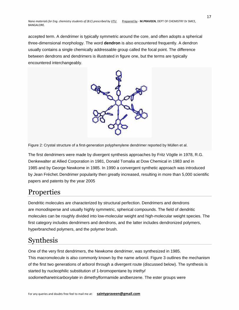
Figure 2: Crystal structure of a first-generation polyphenylene dendrimer reported by Müllen et al.
The first dendrimers were made by divergent synthesis approaches by Fritz Vögtle in 1978, R.G.
Denkewalter at Allied Corporation in 1981, Donald Tomalia at Dow Chemical in 1983 and in
1985 and by George Newkome in 1985. In 1990 a convergent synthetic approach was introduced
by Jean Fréchet. Dendrimer popularity then greatly increased, resulting in more than 5,000 scientific
papers and patents by the year 2005
Properties
Dendritic molecules are characterized by structural perfection. Dendrimers and dendrons
are monodisperse and usually highly symmetric, spherical compounds. The field of dendritic
molecules can be roughly divided into low-molecular weight and high-molecular weight species. The
first category includes dendrimers and dendrons, and the latter includes dendronized polymers,
hyperbranched polymers, and the polymer brush.
Synthesis
One of the very first dendrimers, the Newkome dendrimer, was synthesized in 1985.
This macromolecule is also commonly known by the name arborol. Figure 3 outlines the mechanism
of the first two generations of arborol through a divergent route (discussed below). The synthesis is
started by nucleophilic substitution of 1-bromopentane by triethyl
sodiomethanetricarboxylate in dimethylformamide andbenzene. The ester groups were
18 Nano materials for Eng. chemistry students of (B.E) prescribed by VTU Prepared by - M.PRAVEEN, DEPT OF CHEMISTRY Dr SMCE, BANGALORE.
For any queries and doubts free feel to mail me at: [email protected]
then reduced by lithium aluminium hydride to a triol in a deprotection step. Activation of the chain
ends was achieved by converting the alcohol groups to tosylate groups with tosyl
chloride and pyridine. The tosyl group then served as leaving groups in another reaction with the
tricarboxylate, forming generation two. Further repetition of the two steps leads to higher generations
of arborol.
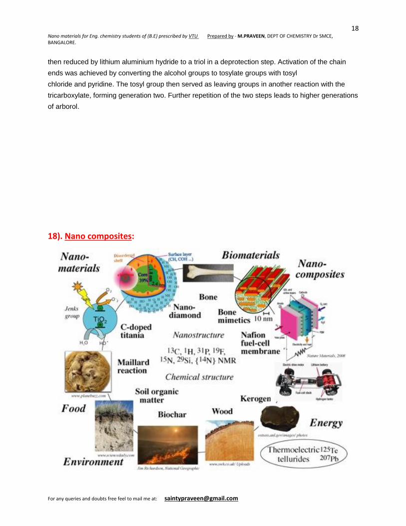
18). Nano composites:

19 Nano materials for Eng. chemistry students of (B.E) prescribed by VTU Prepared by - M.PRAVEEN, DEPT OF CHEMISTRY Dr SMCE, BANGALORE.
For any queries and doubts free feel to mail me at: [email protected]
Nanocomposite is a multiphase solid material where one of the phases has one, two or
three dimensions of less than 100 nanometers (nm), or structures having nano-scale repeat
distances between the different phases that make up the material. In the broadest sense this
definition can include porous media, colloids, gels and copolymers, but is more usually taken to
mean the solid combination of a bulk matrix and nano-dimensional phase(s) differing in properties
due to dissimilarities in structure and chemistry. The mechanical, electrical, thermal, optical,
electrochemical, catalytic properties of the nanocomposite will differ markedly from that of the
component materials. Size limits for these effects have been proposed, <5 nm for catalytic activity,
<20 nm for making a hard magnetic material soft, <50 nm for refractive index changes, and <100 nm
for achieving superparamagnetism, mechanical strengthening or restricting
matrix dislocation movement.
Nanocomposite are found in nature, for example in the structure of the abalone shell and
bone. The use of nanoparticle-rich materials long predates the understanding of the physical and
chemical nature of these materials. Some researchers investigated the origin of the depth of colour
and the resistance to acids and bio-corrosion of blue paint, attributing it to a nanoparticle
mechanism. From the mid-1950s nanoscale organo-clays have been used to control flow of polymer
solutions (e.g. as paint viscosifiers) or the constitution of gels (e.g. as a thickening substance in
cosmetics, keeping the preparations in homogeneous form). By the 1970s polymer/clay composites
were the topic of textbooks,[3] although the term "nanocomposites" was not in common use.