Embed Size (px)
Citation preview
Arrays of Iso-Oriented Gold NanobeltsYing Chen, Srdjan Milenkovic, and Achim Walter Hassel*
Max-Planck-Institut fu¨r Eisenforschung GmbH, Max-Planck Str. 1,D-40237 Dusseldorf, Germany
Received October 7, 2007; Revised Manuscript Received December 16, 2007
ABSTRACT
For the first time single crystalline gold nanobelt arrays with identical crystallographic orientation were obtained. A combined method consistin gof directional solid-state transformation of a Fe −Au eutectoid and a well controlled electrochemical treatment enables production of arrays ofnanobelts with a desired length. They have an average thickness of 25 nm and width of 200 −250 nm, respectively. The obtained gold nanobeltarrays were characterized by electron backscattered diffraction (EBSD), X-ray diffraction, and XPS. The underlying mechanisms and the potentialof this method for the production of nanosensors are discussed.
Intensive approaches have been devoted to the systematiccontrol of the crystal shapes and arrays of metal nanoma-terials, for their applications in physics and for the fabricationof nanodevices.1-3 The intrinsic properties of metal nano-structures can be tuned by controlling size, shape, arrange-ment, and crystallinity.4-5 One-dimensional metallic nano-structures, such as nanowires, nanorods, and nanobelts(nanoribbons), have attracted significant research interesttaking advantage of their promising mechanical, electronic,optical, and other properties with respect to dimensionalityand size confinement.6-7 Nanobelts, especially nanobeltscomposed of semiconductors, have been extensively studiedbecause they may represent a good system for examiningdimensionally confined transport phenomena and for fabri-cating functional nanodevices based on individual nanobelts.8
There are many reports about the preparation of oxides8-10
and sulfides;11-12 however, the report on the synthesis ofmetal nanobelts, especially noble metal nanobelts, is rarelyseen. The only known examples are the preparation of Agnanobelts by refluxing an aqueous silver colloidal disper-sion13 or by reduction of AgNO3 with ascorbic acid in thepresence of poly(acrylic acid) (PAA);14 the growth of Cunanobelts on the surface of an Al TEM grid by galvanicreduction;15 and the growth of Ni nanobelts through ahydrothermal method.16 Very recently, Han et al. reportedon the synthesis of gold nanobelts dispersed in solution byreduction of HAuCl4 with R-D-glucose under sonification;17
and Zhang et al. prepared gold nanobelts via one-dimensionalself-assembly of triangular Au nanoplates.18
Nanoarrays on a surface have a potential for applicationsin optoelectronics, information storage, and electrochemicalsensing.19 For example, when gold nanowires are organizedin an array, the resulting electrodes could combine the
advantages of both, that of a nanoelectrode and the signalintensity from a macroscopic electrode. Among variousfabrication methods of nanoarrays, the so-called “template”method, named by C. R. Martin,20 especially a “hard”template such as Anodized Aluminum Oxide (AAO), wasextensively studied due to its controllable effect on productsize and shape through the template structure. Therefore, thistemplate method has been widely used to prepare nanostruc-tures with various morphologies such as nanowires, nano-tubes, nanowells, nanopillars, and even nanobarcodes com-posed of different metals or a combination of metal andsemiconductor.19-25 For the preparation of gold nanowires,Sander19 produced gold nanodot arrays by evaporation andgold nanorod arrays by electrochemical deposition; Wirtz21
used electrochemical deposition into the AAO template tofabricate gold nanowire and nanotube arrays to form goldnanoelectrodes; Forrer26 used the same method to form goldnanowire arrays. However, these nanowires are usuallypolycrystalline, which is often a drawback for their applica-tions. Only in a few cases the wires show a high degree ofcrystallinity27-28 but no crystallographic orientation relation-ship among the wires. The drawback can be, for example, aquantitative description of spectroscopic properties of goldnanowires cannot be achieved, because of the differentadsorption abilities for molecules on different crystal-lographic surfaces.29 So, it is quite interesting but alsochallenging to fabricate one-dimensional gold nanostructurearrays, which can find practical applications in nanodevices.30
Here, it is reported on a method for synthesizing single-crystalline gold nanobelt arrays, embedded in an iron matrix,through directional solidification of an Fe-Au eutectoidalloy. Directional solidification of a eutectic/eutectoid alloyis a method that can facilitate the nanostructuring of amaterial. It includes directional decomposition of theFe-Au eutectoid alloy, followed by a phase separation
* Corresponding author. E-mail: [email protected]. Fax:+49 2116792 218.
NANOLETTERS
2008Vol. 8, No. 2
737-742
10.1021/nl0725852 CCC: $40.75 © 2008 American Chemical SocietyPublished on Web 02/13/2008

through selective and partial etching of the Fe matrix torelease gold nanobelts from the matrix.
This method has several advantages. It produces singlecrystalline nanobelt arrays embedded in a single crystallinematrix. These gold nanobelts have identical crystallographicorientations even azimuthally in one grain. Nanobelt size andspacing show a narrow distribution and can be controlledby the processing parameters.31 The spacing between eachnanobelt is large enough to study the properties of a singlenanobelt. To the best of the authors’ knowledge, this is thefirst example of monocrystalline iso-oriented Au nanobeltarrays reported up to date.
In a previous study, it was confirmed that the eutectoidtransformation occurs at 2.3 at. % Au,32 which agreed wellwith existing calculated and DTA data.33 Pre-alloys wereprepared using 99.999% Au and 5 times zone melting refinedFe, by induction melting under an Ar atmosphere and dropcasting into a cylindrical copper mould. After subsequentfitting into alumina crucibles, samples were directionallytransformed in a Bridgman type solidification furnace withresistance heating. The details were described elsewhere.32
Further, the eutectoid alloy was cut in 1× 1 × 0.1 cm3 piecesand ground for further treatment. The selective and partialdissolution of theR-Fe phase in the eutectoid alloy wasachieved through electrochemical etching by anodic dissolu-tion. The electrolyte was only slightly different from thatfor electrochemical polishing for pure iron and was composedof 20 mL of HClO4 and 180 mL of 2-butoxyethanol; thenonaqueous electrolyte was used in order to avoid thehydrolysis of Fe ions. All electrochemical etching experi-ments were performed at 0°C to reduce the possibleoxidation of ferrous ions. The applied potential varied from1.5 to 8.0 V (vs counter electrode), and the time of etchingwas varied between 1 and 30 min. After this procedure, thesample was washed with ethanol, dried, and stored in adesiccator for future characterization.
In order to obtain gold nanobelt arrays with a smoothmatrix surface, high potentials were applied to accelerate theetching process, meanwhile, to avoid the local corrosion ofiron. After the etching at 5 V (vs counter electrode) for 5min, arrays of short gold nanobelts were obtained, as shownin Figure 1. Figure 1a and b show the representative fieldemission scanning electron microscopy images (FE-SEM,LEO 1550VP, GEMINI) of the as-prepared “short” goldnanobelt arrays. Figure 1c shows the high-resolutionFE-SEM image of these gold nanobelt arrays. The size ofthe nanobelts was determined from the SEM images. Theyhave an average thickness of 25 nm, a width of 200-250nm, and an exposed length of less than 200 nm.
The crystallinity and crystallographic orientation of theobtained gold nanobelt arrays were characterized using anelectron backscattering diffraction technique (EBSD, TSL/EDAX, DigiView 1612 camera). To determine the crystal-linity and the crystallographic orientation relationship of thegold nanobelts, some gold nanobelts were randomly chosen.First, the short gold nanobelts were cut along the matrixsurface with a focused ion beam (FIB, Zeiss XB 1560,equipped with a field emission electron column and a
Gallium ion emitter) to get a smooth surface, which is vitalfor EBSD. The high-quality Kikuchi patterns were clearlyobserved as shown in Figure 2, and by indexing them, thecorresponding Euler angles (æ1, Φ, æ2) were obtained.Figure 2 shows the Kikuchi patterns of two randomlyselected gold nanobelts (a and b) and two different spots ofthe matrix (c and d), respectively. The results demonstratethat both, the matrix and the belts are single crystalline.Moreover, in one grain, not only the matrix iron has identicalcrystallographic orientation at different randomly chosenspots but also the different gold nanobelts have the samecrystallographic orientation, even azimuthally. This meansthat the obtained arrays consist of iso-oriented singlecrystalline gold nanobelts. It should be pointed out that,because it is very difficult to find the exact position wheregold nanobelts are perpendicular to the surface, the obtainedcrystallographic orientations of gold nanobelts may be notexactly the growth direction of the nanobelts. This is part ofan ongoing project, and the new result will be reported.
Figure 1. (a, b) FE-SEM images and (c) high-magnification SEMimage of as-prepared Au nanobelt arrays; potentialE ) 5 V, etchingtime t ) 5 min.
738 Nano Lett., Vol. 8, No. 2, 2008

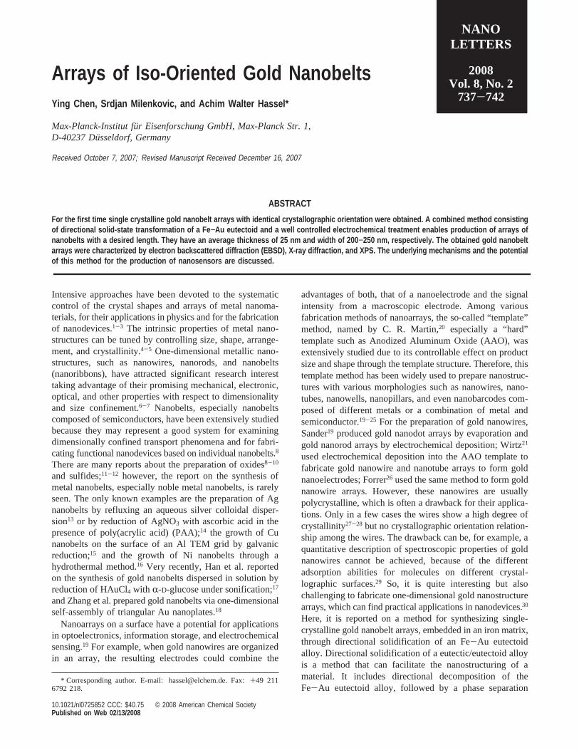
X-ray diffraction (XRD, BRUKER axs, D8 X-ray diffrac-tometer) gives further support of the phase structure of theobtained gold nanobelt arrays. Curves in Figure 3 a and bshow the diffraction patterns for gold nanobelt arrays beforeand after partial etching. As shown in Figure 3b, the peakslocated at 2θ ) 38.184°, 2θ ) 44.392°, and 2θ ) 64.576°correspond to the (111), (200), and (220) lattice planes ofthe face-centered cubic (fcc) structure of gold (JCPDS, FileNo. 4-0784). Moreover, from Figure 3a, which is the XRDof the sample prior to etching, the difference compared tothat of the partially etched sample (Figure 3b) can be clearlyseen. The peaks located at 2θ ) 44.673° and 2θ ) 65.021°correspond to the (110) and (200) lattice planes of body-centered cubic (bcc)R-iron (JCPDE, File No. 6-0696). Thepeak of (200) of gold is very near to the peak of (110) ofR-iron (0.281° difference), and the peak of (220) of gold isalso quite near to the peak of (200) ofR-iron (0.445°difference); therefore it is difficult to deconvolute the peaks
located at 2θ of 44.5° and 64.5°. For the fcc gold, thestrongest peak is located at 2θ ) 38.184°, and forR-iron itis at 2θ ) 44.673°, so the peak intensity at 2θ ) 38.184°,2θ ) 44.5°, and 2θ ) 64.5° can be calculated by multiplyingthe individual peak intensity with the alloy composition. Theresult is shown in Table 1. The experimental results of thenonetched sample are quite similar to the calculated results,whereas, for the partially etched sample, the peak located atabout 2θ ) 38.184° is much stronger than the calculatedone. This is clear proof that gold nanobelts of identicalorientation are released through this etching process. Thegold nanobelt arrays were additionally characterized by X-rayphotoelectron spectroscopy (XPS, Physical Electronics Quan-tum 2000 Scanning ESCA Microprobe, sputtering 2 keVAr+). The XPS results (Figure 4) show that the goldnanobelts are pure metallic gold, which can be confirmedfrom the binding energy for Au 4f7/2 located at 84 eV, andthat the matrix is covered with a thin layer of iron oxide
Figure 2. EBSD patterns of Au (a and b) and Fe (c and d) in one sample, which proved that gold nanobelts have the same crystallographicorientation.
Nano Lett., Vol. 8, No. 2, 2008 739
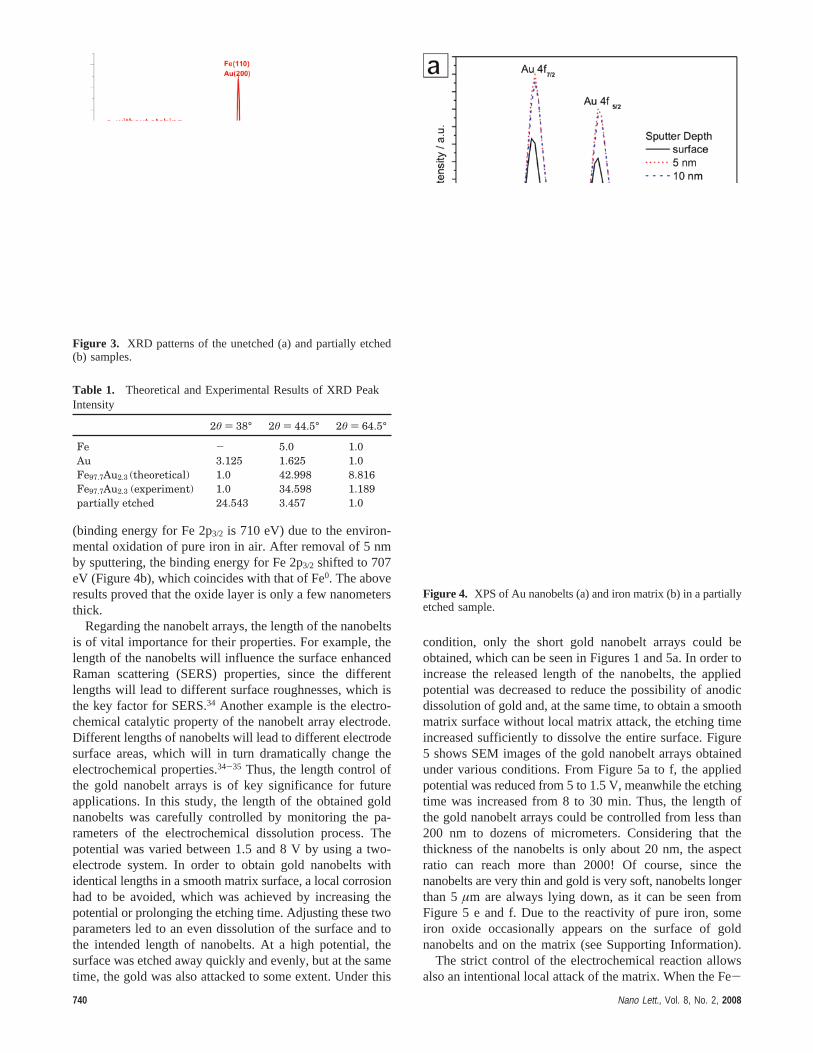
(binding energy for Fe 2p3/2 is 710 eV) due to the environ-mental oxidation of pure iron in air. After removal of 5 nmby sputtering, the binding energy for Fe 2p3/2 shifted to 707eV (Figure 4b), which coincides with that of Fe0. The aboveresults proved that the oxide layer is only a few nanometersthick.
Regarding the nanobelt arrays, the length of the nanobeltsis of vital importance for their properties. For example, thelength of the nanobelts will influence the surface enhancedRaman scattering (SERS) properties, since the differentlengths will lead to different surface roughnesses, which isthe key factor for SERS.34 Another example is the electro-chemical catalytic property of the nanobelt array electrode.Different lengths of nanobelts will lead to different electrodesurface areas, which will in turn dramatically change theelectrochemical properties.34-35 Thus, the length control ofthe gold nanobelt arrays is of key significance for futureapplications. In this study, the length of the obtained goldnanobelts was carefully controlled by monitoring the pa-rameters of the electrochemical dissolution process. Thepotential was varied between 1.5 and 8 V by using a two-electrode system. In order to obtain gold nanobelts withidentical lengths in a smooth matrix surface, a local corrosionhad to be avoided, which was achieved by increasing thepotential or prolonging the etching time. Adjusting these twoparameters led to an even dissolution of the surface and tothe intended length of nanobelts. At a high potential, thesurface was etched away quickly and evenly, but at the sametime, the gold was also attacked to some extent. Under this
condition, only the short gold nanobelt arrays could beobtained, which can be seen in Figures 1 and 5a. In order toincrease the released length of the nanobelts, the appliedpotential was decreased to reduce the possibility of anodicdissolution of gold and, at the same time, to obtain a smoothmatrix surface without local matrix attack, the etching timeincreased sufficiently to dissolve the entire surface. Figure5 shows SEM images of the gold nanobelt arrays obtainedunder various conditions. From Figure 5a to f, the appliedpotential was reduced from 5 to 1.5 V, meanwhile the etchingtime was increased from 8 to 30 min. Thus, the length ofthe gold nanobelt arrays could be controlled from less than200 nm to dozens of micrometers. Considering that thethickness of the nanobelts is only about 20 nm, the aspectratio can reach more than 2000! Of course, since thenanobelts are very thin and gold is very soft, nanobelts longerthan 5µm are always lying down, as it can be seen fromFigure 5 e and f. Due to the reactivity of pure iron, someiron oxide occasionally appears on the surface of goldnanobelts and on the matrix (see Supporting Information).
The strict control of the electrochemical reaction allowsalso an intentional local attack of the matrix. When the Fe-
Figure 3. XRD patterns of the unetched (a) and partially etched(b) samples.
Table 1. Theoretical and Experimental Results of XRD PeakIntensity
2θ ) 38° 2θ ) 44.5° 2θ ) 64.5°
Fe - 5.0 1.0Au 3.125 1.625 1.0Fe97.7Au2.3 (theoretical) 1.0 42.998 8.816Fe97.7Au2.3 (experiment) 1.0 34.598 1.189partially etched 24.543 3.457 1.0
Figure 4. XPS of Au nanobelts (a) and iron matrix (b) in a partiallyetched sample.
740 Nano Lett., Vol. 8, No. 2, 2008

Au eutectoid alloy sample was cut along the growth direction(along the axis of the cylinder ingot), the gold nanobelts areembedded in the matrix parallel to the surface. The SEMimages shown in Figure 6, which were taken from alongitudinally cut sample anodized at a low potential for ashort time (5 V, 1 min), confirm the abovementionedprediction. The gold nanobelts can be clearly seen embeddedinside of the matrix and parallel to the surface. Similarfeatures were observed in the NiAl-Re eutectic system,
when the sample was anisotropically etched parallel to thegrowth direction.36 In that case Re nanowires were stretchingthrough the pits parallel to the sample surface. This kind of“bridging” nanostructures could be employed in the me-chanical testing of nanowires or nanobelts.
In summary, for the first time, gold nanoarrays of singlecrystalline gold nanobelts with long-range identical crystal-lographic orientation were obtained. Directional solid-statetransformation of an Fe-Au eutectoid followed by a
Figure 5. SEM images of nanobelt arrays with different lengths (a) 250 nm, (b) 500 nm, (c) 1µm, (d) 2µm, (e) 10µm, and (f) 30µm.
Figure 6. SEM images of general view (a) and a typical pitting hole of the sample in which gold nanobelts are parallel to the surface (b).
Nano Lett., Vol. 8, No. 2, 2008 741
precisely controllable electrochemical treatment enabled theproduction of arrays with iso-oriented nanobelts of a desiredlength. The method is simple, convenient, economical, andeasily applicable on a large scale. These unique propertiesallow a quantitative study of the spectroscopic properties asa function of the electrochemical potential and crystal-lographic orientation. Moreover, the obtained gold nanobeltarrays can later be used as nanosensors and/or nanoelectrodesafter appropriate insulation of the interspace left afterdissolution of the matrix.
Acknowledgment. Ying Chen acknowledges IMPRSSurmat for financial support through a fellowship. Thefinancial support of the Deutsche-Forschungs-Gemeinschaftthrough the project Application of Directionally SolidifiedNanowire Arrays within the DFG Priority Programme 1165Nanowires and Nanotubes - From Controlled Synthesis toFunction is gratefully acknowledged. Dedicated to Prof.Dieter M Kolb on the occasion of his 65th birthday.
Supporting Information Available: Detailed descrip-tions of materials and methods, as well as additional figures.This material is available free of charge via the Internet athttp://pubs.acs.org.
References
(1) Wang, Z. L.J. Phys. Chem. B2000, 104, 1153.(2) Murphy, C. J.Science2002, 298, 2139.(3) Narayana, R.; El-Sayed, M. A.Nano Lett.2004, 4, 1343.(4) Jin, R.; Cao, Y.; Kelly, C. A.; Schatz, G. C.; Zheng, J. G.Science
2001, 294, 1901.(5) El-Sayed, M. A.Acc. Chem. Res.2001, 34, 257.(6) Chen, J.; Wiley, B. J.; Xia, Y.Langmuir2007, 23, 4120.(7) Murphy, C. J.; Sau, T. K.; Gole, A. M.; Orendorff, C. J.; Gao, J.;
Gou, L.; Hunyadi, S. E.; Li, T.J. Phys. Chem. B2005, 109, 13857.(8) Pan, Z. W.; Dai, Z. R.; Wang, Z. L.Science2001, 291, 1947.(9) Wen, X.; Wang, S.; Ding, Y.; Wang, Z. L.; Yang, S.J. Phys. Chem.
B 2005, 109, 215.(10) Ma, R.; Bando, Y.; Zhang, L.; Sasaki, T.AdV. Mater.2004, 16, 918.(11) Yao, W. T.; Yu, S. H.; Pan, L.; Li, J.; Wu, Q. S.; Zhang, L.; Jiang,
J. Small2005, 1, 320.
(12) Zhu, Y. C.; Bando, Y.; Xue, D. F.Appl. Phys. Lett.2003, 82, 1769.(13) Bai, J.; Qin, Y.; Jiang, C.; Qi, L.Chem. Mater.2007, 19, 3367.(14) Sun, Y.; Mayers, B.; Xia, Y.Nano Lett.2003, 3, 675.(15) Huang, T. K.; Cheng, T. H.; Yen, M. Y.; Hsiao, W. H.; Wang, L.
S.; Chen, F. R.; Kai, J. J.; Lee, C. Y.; Chiu, H. T.Langmuir2007,23, 5722.
(16) Liu, Z.; Li, S.; Yang, Y.; Peng, S.; Hu, Z.; Qian, Y.AdV. Mater.2003, 15, 1946.
(17) Zhang, J.; Du, J.; Han, B.; Liu, Z.; Jiang, T.; Zhang, Z.Angew. Chem.,Int. Ed. 2006, 45, 1116.
(18) Zhang, J.; Liu, H.; Wang, Z.; Ming, N.Appl. Phys. Lett.2007, 91,133112.
(19) Sander, M. S.; Tan, L. S.AdV. Funct. Mater.2003, 13, 393.(20) Martin, C. R.Science1994, 266, 1981.(21) Wirtz, M.; Martin, C. R.AdV. Mater. 2003, 15, 445.(22) Evans, U.; Colavita, P. E.; Doescher, M. S.; Schiza, M.; Myrick, M.
L. Nano Lett.2002, 2, 641.(23) Yuan, J.; Wang, K.; Xia, X.AdV. Funct. Mater.2005, 15, 803.(24) Nicewarner-Pena, S. R.; Freeman, R. G.; Reiss, B. D.; He, L.; Pena,
D. J.; Walton, I. D.; Cromer, R.; Keating, C. D.; Natan, M. J.Science2001, 294, 137.
(25) Lee, J. H.; Wu, J. H.; Liu, H. L.; Cho, J. U.; Cho, M. K.; An, B. H.;Min, J. H.; Noh, S. J.; Kim, Y. K.Angew. Chem., Int. Ed.2007, 46,3663.
(26) Forrer, P.; Schlottig, F.; Siegenthaler, H.; Textor, M.J. Appl.Electrochem.2000, 30, 533.
(27) Karim, S.; Toimil-Molares, M. E.; Maurer, F.; Miehe, G.; Ensinger,W.; Liu, J.; Cornelius, T. W.; Neumann, R.Appl. Phys. A.2006, 84,403.
(28) Tian, M.; Wang, J.; Kurtz, J.; Mallouk, T. E.; Chan, M. H. W.NanoLett. 2003, 3, 919.
(29) Kamat, P. V.J. Phys. Chem. B2002, 106, 7729.(30) Hassel, A. W.; Smith, A. J.; Milenkovic, S.Electrochim. Acta2006,
52, 1799.(31) Milenkovic, S.; Hassel, A. W.; Schneider, A.Nano Lett.2006, 6,
794.(32) Milenkovic, S.; Schneider, A.; Hassel, A. W.Gold Bull. 2006, 39,
185.(33) Isaac, E.; Walter, P.Z. Anorg. Metallkd.1950, 41, 234.(34) Tian, Z. Q.; Ren, B.; Wu, D. Y.J. Phys. Chem. B2002, 106, 9463.(35) Gao, F. F.; El-Deab, M. S.; Okajima, T.; Ohsaka, T.J. Electrochem.
Soc.2005, A1226.(36) Hassel, A. W.; Bello-Rodriguez, B.; Milenkovic, S.Electrochim. Acta
2005, 51, 795.
NL0725852
742 Nano Lett., Vol. 8, No. 2, 2008


![VERIFICATION-ORIENTED PROOF RULES FOR ARRAYS, … · D D C SULQEJiT JM Jt'L «7 f976 ... Verification- Oriented Proof Rules for Arrays, Records and Pointers ... [Hoar« 69] it ontiroiy](https://img.pdfslide.us/doc/110x75/5c68126509d3f22d638cef97/verification-oriented-proof-rules-for-arrays-d-d-c-sulqejit-jm-jtl-7-f976.jpg)