Embed Size (px)
Citation preview
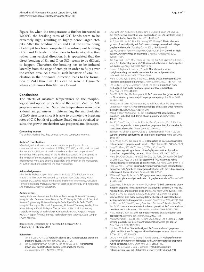
Ahmad et al. Nanoscale Research Letters 2014, 9:83http://www.nanoscalereslett.com/content/9/1/83
NANO EXPRESS Open Access
Seed/catalyst-free growth of zinc oxidenanostructures on multilayer graphene bythermal evaporationNurul Fariha Ahmad1, Nurul Izni Rusli2, Mohamad Rusop Mahmood3, Kanji Yasui4 and Abdul Manaf Hashim1,5*
Abstract
We report the seed/catalyst-free growth of ZnO on multilayer graphene by thermal evaporation of Zn in thepresence of O2 gas. The effects of substrate temperatures were studied. The changes of morphologies were verysignificant where the grown ZnO structures show three different structures, i.e., nanoclusters, nanorods, and thinfilms at 600°C, 800°C, and 1,000°C, respectively. High-density vertically aligned ZnO nanorods comparable to othermethods were obtained. A growth mechanism was proposed based on the obtained results. The ZnO/graphenehybrid structure provides several potential applications in electronics and optoelectronics.
Keywords: Graphene; Thermal evaporation; Zinc oxide; Nanostructure; Hybrid integration
BackgroundIn recent years, strong attentions have been paid in thegrowth of semiconductor nanostructures on graphene[1-5] for electronic and optoelectronic applications. Nano-structures such as nanowires, nanorods, nanoneedles,nanosheets, and nanowalls can offer additional func-tionality to graphene for realizing advanced nanoscaleapplications in photovoltaics, nanogenerators, field emis-sion devices, sensitive biological and chemical sensors,and efficient energy conversion and storage devices [6-8].This is due to the superb properties of nanostructuressuch as high aspect ratio, extremely large surface-to-volume ratio, and high porosity [6-10]. Graphene has agreat potential for novel electronic devices because of itsextraordinary electrical, thermal, and mechanical proper-ties, including carrier mobility exceeding 104 cm2/Vs anda thermal conductivity of 103 W/mK [11-14]. Therefore,with the excellent electrical and thermal characteristics ofgraphene layers, growing semiconductor nanostructureson graphene layers would enable their novel physicalproperties to be exploited in diverse sophisticated deviceapplications. Graphene is a 2D hexagonal network of
* Correspondence: [email protected] International Institute of Technology, Universiti TeknologiMalaysia, Jalan Semarak, Kuala Lumpur 54100, Malaysia5MIMOS Berhad, Technology Park Malaysia, Kuala Lumpur 57000, MalaysiaFull list of author information is available at the end of the article
© 2014 Ahmad et al.; licensee Springer. This isAttribution License (http://creativecommons.orin any medium, provided the original work is p
carbon atoms which is formed by making strong tri-angular σ-bonds of the sp2 hybridized orbitals. Thisbonding structure is similar to the (111) plane of zinc-blende structure and C plane of a hexagonal crystallinestructure. With this regard, the growth of semicon-ductor nanostructures and thin films on graphene isfeasible. Recently, there are several works on the growthand application of graphene/semiconductor nanocrystalsthat show desirable combinations of these properties notfound in the individual components [15-20].The 1D zinc oxide (ZnO) semiconducting nanostruc-
tures are considered to be important multifunctionalbuilding blocks for fabricating various nanodevices [21,22].Since graphene is an excellent conductor and transparentmaterial, the hybrid structure of ZnO/graphene shall leadto several device applications not only on Si substrate butalso on other insulating substrates such as transparentglass and transparent flexible plastic. Owing to the uniqueelectronic and optical properties of ZnO nanostructures,such hybrid structure can be used for sensing devices[23-25], UV photodetector [26], solar cells [27], and light-emitting diodes [28]. ZnO nanostructures have beensynthesized by various physical and chemical growthtechniques [23]. These techniques include thermal evapor-ation [5,29], hydrothermal [2,3] and electrochemical depos-ition [4], and metal-organic vapor-phase epitaxy (MOVPE)[1]. In this paper, we report the seed/catalyst-free growth of
an Open Access article distributed under the terms of the Creative Commonsg/licenses/by/2.0), which permits unrestricted use, distribution, and reproductionroperly credited.
Ahmad et al. Nanoscale Research Letters 2014, 9:83 Page 2 of 7http://www.nanoscalereslett.com/content/9/1/83
ZnO structures on multilayer (ML) graphene by thermalevaporation. The dependence of substrate temperatures onthe properties of grown structures was studied. Based onthe obtained results, a growth mechanism was proposed.
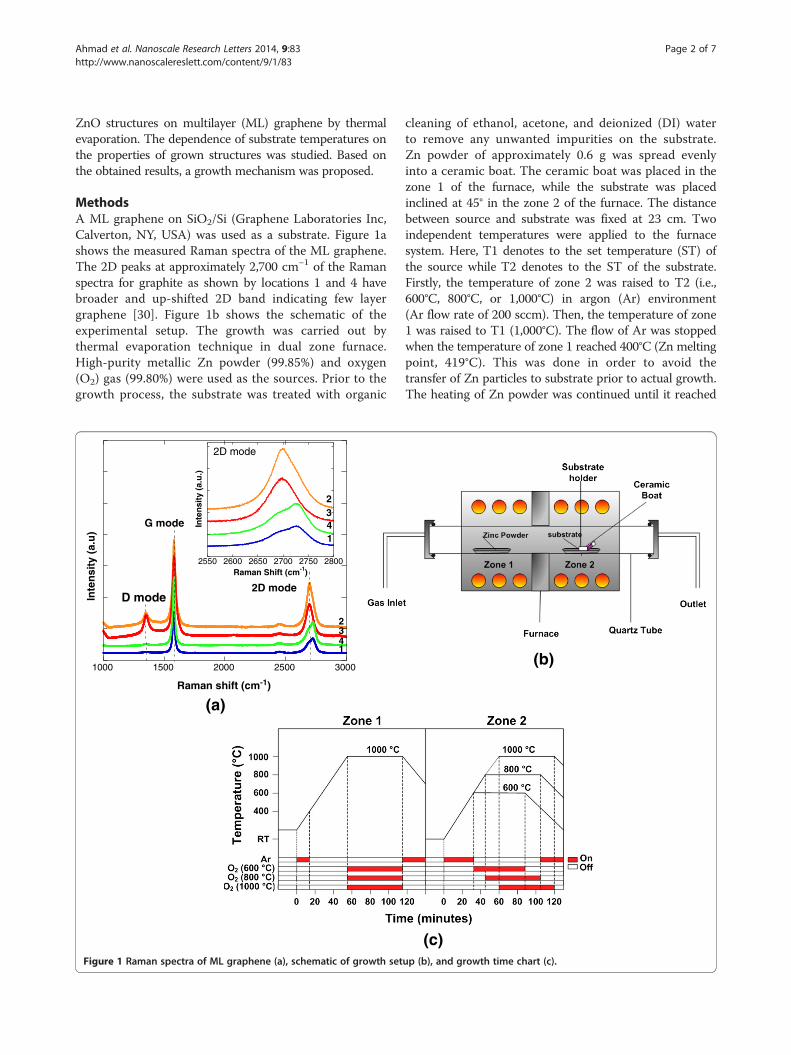
MethodsA ML graphene on SiO2/Si (Graphene Laboratories Inc,Calverton, NY, USA) was used as a substrate. Figure 1ashows the measured Raman spectra of the ML graphene.The 2D peaks at approximately 2,700 cm−1 of the Ramanspectra for graphite as shown by locations 1 and 4 havebroader and up-shifted 2D band indicating few layergraphene [30]. Figure 1b shows the schematic of theexperimental setup. The growth was carried out bythermal evaporation technique in dual zone furnace.High-purity metallic Zn powder (99.85%) and oxygen(O2) gas (99.80%) were used as the sources. Prior to thegrowth process, the substrate was treated with organic
1000 1500 2000 2500 3000
Inte
nsi
ty (
a.u
)
Raman shift (cm-1)
2D mode
G mode
D mode
1
234
2550 2600 2650 2700 2750 2800
Inte
nsi
ty (
a.u
.)
Raman Shift (cm-1)
2D mode
1432
(a)
Figure 1 Raman spectra of ML graphene (a), schematic of growth set
cleaning of ethanol, acetone, and deionized (DI) waterto remove any unwanted impurities on the substrate.Zn powder of approximately 0.6 g was spread evenlyinto a ceramic boat. The ceramic boat was placed in thezone 1 of the furnace, while the substrate was placedinclined at 45° in the zone 2 of the furnace. The distancebetween source and substrate was fixed at 23 cm. Twoindependent temperatures were applied to the furnacesystem. Here, T1 denotes to the set temperature (ST) ofthe source while T2 denotes to the ST of the substrate.Firstly, the temperature of zone 2 was raised to T2 (i.e.,600°C, 800°C, or 1,000°C) in argon (Ar) environment(Ar flow rate of 200 sccm). Then, the temperature of zone1 was raised to T1 (1,000°C). The flow of Ar was stoppedwhen the temperature of zone 1 reached 400°C (Zn meltingpoint, 419°C). This was done in order to avoid thetransfer of Zn particles to substrate prior to actual growth.The heating of Zn powder was continued until it reached
(b)
(c)up (b), and growth time chart (c).
Ahmad et al. Nanoscale Research Letters 2014, 9:83 Page 3 of 7http://www.nanoscalereslett.com/content/9/1/83
1,000°C. It was confirmed from several attempts that suchhigh temperature was needed for continuous and constantevaporation of Zn. After reaching 1,000°C, O2 (400 sccm)was introduced for 1 h of growth time. Finally, the furnacewas turned off and the samples were cooled down toroom temperature. Figure 1c summarizes the growthprocedures. The as-grown ZnO was examined usingfield-emission scanning electron (FESEM) microscopy(SU8030, Hitachi, Chiyoda, Tokyo, Japan), dispersiveX-ray (EDX) spectroscopy, X-ray diffraction (XRD) (Bruker,AXES, D8 Advance, Bruker Corporation, Billerica, MA,USA) and photoluminescence (PL) spectroscopy (HoribaJobinYvon, Tokyo, Japan).
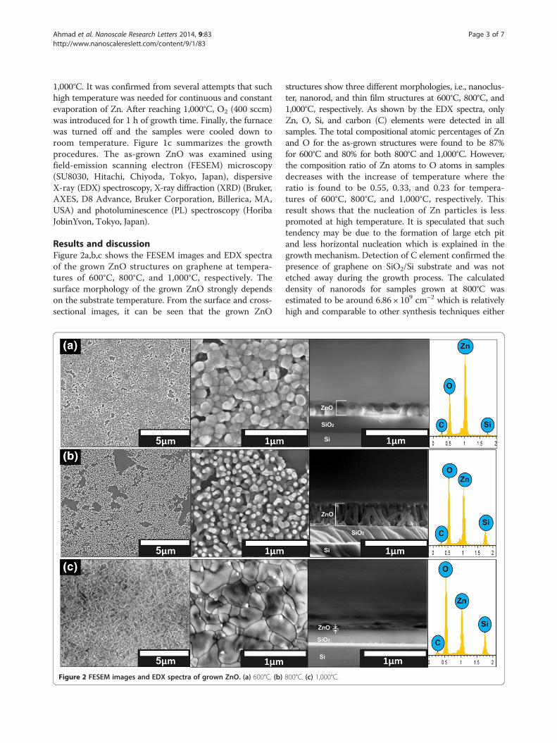
Results and discussionFigure 2a,b,c shows the FESEM images and EDX spectraof the grown ZnO structures on graphene at tempera-tures of 600°C, 800°C, and 1,000°C, respectively. Thesurface morphology of the grown ZnO strongly dependson the substrate temperature. From the surface and cross-sectional images, it can be seen that the grown ZnO
Figure 2 FESEM images and EDX spectra of grown ZnO. (a) 600°C. (b)
structures show three different morphologies, i.e., nanoclus-ter, nanorod, and thin film structures at 600°C, 800°C, and1,000°C, respectively. As shown by the EDX spectra, onlyZn, O, Si, and carbon (C) elements were detected in allsamples. The total compositional atomic percentages of Znand O for the as-grown structures were found to be 87%for 600°C and 80% for both 800°C and 1,000°C. However,the composition ratio of Zn atoms to O atoms in samplesdecreases with the increase of temperature where theratio is found to be 0.55, 0.33, and 0.23 for tempera-tures of 600°C, 800°C, and 1,000°C, respectively. Thisresult shows that the nucleation of Zn particles is lesspromoted at high temperature. It is speculated that suchtendency may be due to the formation of large etch pitand less horizontal nucleation which is explained in thegrowth mechanism. Detection of C element confirmed thepresence of graphene on SiO2/Si substrate and was notetched away during the growth process. The calculateddensity of nanorods for samples grown at 800°C wasestimated to be around 6.86 × 109 cm−2 which is relativelyhigh and comparable to other synthesis techniques either
800°C. (c) 1,000°C.
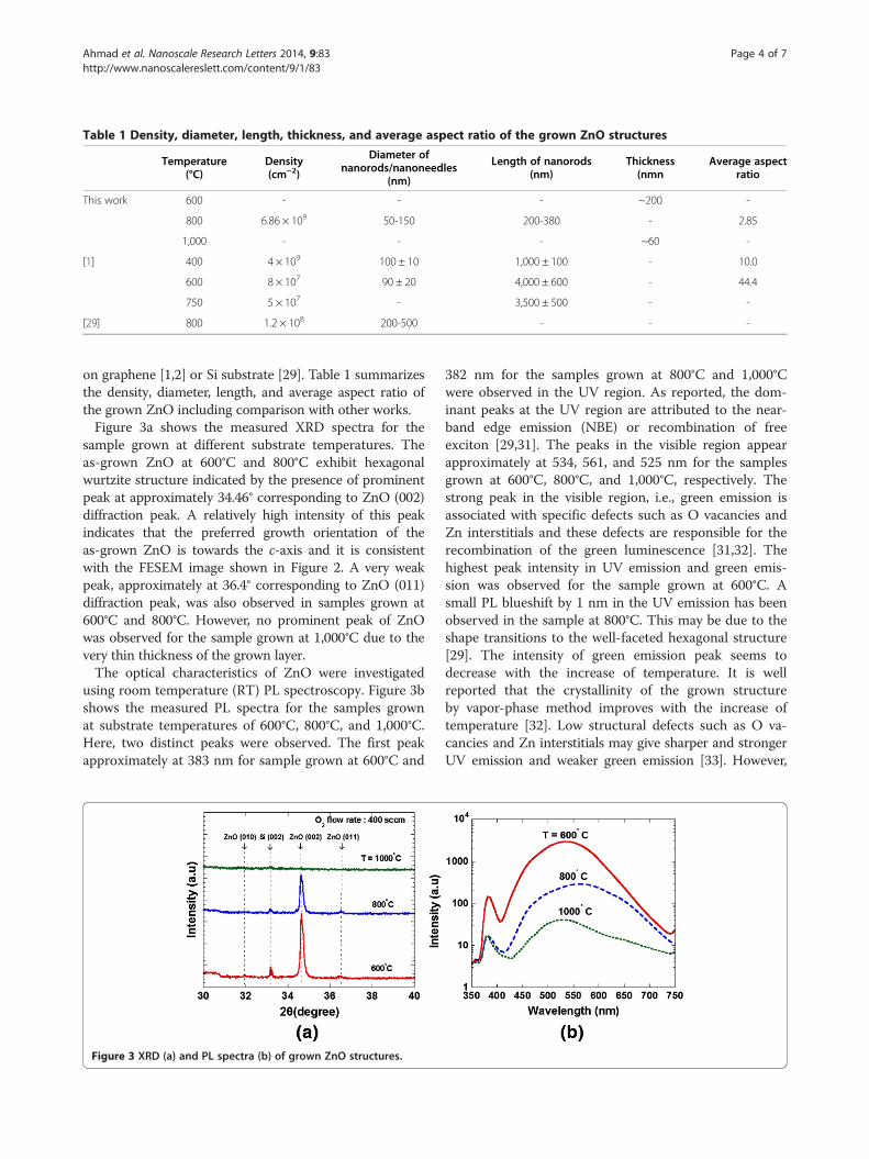
Table 1 Density, diameter, length, thickness, and average aspect ratio of the grown ZnO structures
Temperature(°C)
Density(cm−2)
Diameter ofnanorods/nanoneedles
(nm)
Length of nanorods(nm)
Thickness(nmn
Average aspectratio
This work 600 - - - ~200 -
800 6.86 × 10⁹ 50-150 200-380 - 2.85
1,000 - - - ~60 -
[1] 400 4 × 10⁹ 100 ± 10 1,000 ± 100 - 10.0
600 8 × 10⁷ 90 ± 20 4,000 ± 600 - 44.4
750 5 × 10⁷ - 3,500 ± 500 - -
[29] 800 1.2 × 10⁸ 200-500 - - -
Ahmad et al. Nanoscale Research Letters 2014, 9:83 Page 4 of 7http://www.nanoscalereslett.com/content/9/1/83
on graphene [1,2] or Si substrate [29]. Table 1 summarizesthe density, diameter, length, and average aspect ratio ofthe grown ZnO including comparison with other works.Figure 3a shows the measured XRD spectra for the
sample grown at different substrate temperatures. Theas-grown ZnO at 600°C and 800°C exhibit hexagonalwurtzite structure indicated by the presence of prominentpeak at approximately 34.46° corresponding to ZnO (002)diffraction peak. A relatively high intensity of this peakindicates that the preferred growth orientation of theas-grown ZnO is towards the c-axis and it is consistentwith the FESEM image shown in Figure 2. A very weakpeak, approximately at 36.4° corresponding to ZnO (011)diffraction peak, was also observed in samples grown at600°C and 800°C. However, no prominent peak of ZnOwas observed for the sample grown at 1,000°C due to thevery thin thickness of the grown layer.The optical characteristics of ZnO were investigated
using room temperature (RT) PL spectroscopy. Figure 3bshows the measured PL spectra for the samples grownat substrate temperatures of 600°C, 800°C, and 1,000°C.Here, two distinct peaks were observed. The first peakapproximately at 383 nm for sample grown at 600°C and
Figure 3 XRD (a) and PL spectra (b) of grown ZnO structures.
382 nm for the samples grown at 800°C and 1,000°Cwere observed in the UV region. As reported, the dom-inant peaks at the UV region are attributed to the near-band edge emission (NBE) or recombination of freeexciton [29,31]. The peaks in the visible region appearapproximately at 534, 561, and 525 nm for the samplesgrown at 600°C, 800°C, and 1,000°C, respectively. Thestrong peak in the visible region, i.e., green emission isassociated with specific defects such as O vacancies andZn interstitials and these defects are responsible for therecombination of the green luminescence [31,32]. Thehighest peak intensity in UV emission and green emis-sion was observed for the sample grown at 600°C. Asmall PL blueshift by 1 nm in the UV emission has beenobserved in the sample at 800°C. This may be due to theshape transitions to the well-faceted hexagonal structure[29]. The intensity of green emission peak seems todecrease with the increase of temperature. It is wellreported that the crystallinity of the grown structureby vapor-phase method improves with the increase oftemperature [32]. Low structural defects such as O va-cancies and Zn interstitials may give sharper and strongerUV emission and weaker green emission [33]. However,
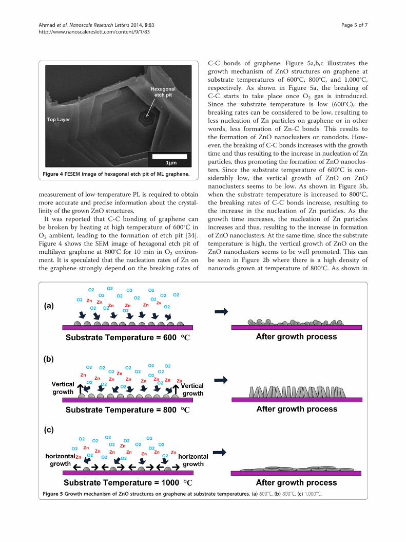
Figure 4 FESEM image of hexagonal etch pit of ML graphene.
Ahmad et al. Nanoscale Research Letters 2014, 9:83 Page 5 of 7http://www.nanoscalereslett.com/content/9/1/83
measurement of low-temperature PL is required to obtainmore accurate and precise information about the crystal-linity of the grown ZnO structures.It was reported that C-C bonding of graphene can
be broken by heating at high temperature of 600°C inO2 ambient, leading to the formation of etch pit [34].Figure 4 shows the SEM image of hexagonal etch pit ofmultilayer graphene at 800°C for 10 min in O2 environ-ment. It is speculated that the nucleation rates of Zn onthe graphene strongly depend on the breaking rates of
Figure 5 Growth mechanism of ZnO structures on graphene at subst
C-C bonds of graphene. Figure 5a,b,c illustrates thegrowth mechanism of ZnO structures on graphene atsubstrate temperatures of 600°C, 800°C, and 1,000°C,respectively. As shown in Figure 5a, the breaking ofC-C starts to take place once O2 gas is introduced.Since the substrate temperature is low (600°C), thebreaking rates can be considered to be low, resulting toless nucleation of Zn particles on graphene or in otherwords, less formation of Zn-C bonds. This results tothe formation of ZnO nanoclusters or nanodots. How-ever, the breaking of C-C bonds increases with the growthtime and thus resulting to the increase in nucleation of Znparticles, thus promoting the formation of ZnO nanoclus-ters. Since the substrate temperature of 600°C is con-siderably low, the vertical growth of ZnO on ZnOnanoclusters seems to be low. As shown in Figure 5b,when the substrate temperature is increased to 800°C,the breaking rates of C-C bonds increase, resulting tothe increase in the nucleation of Zn particles. As thegrowth time increases, the nucleation of Zn particlesincreases and thus, resulting to the increase in formationof ZnO nanoclusters. At the same time, since the substratetemperature is high, the vertical growth of ZnO on theZnO nanoclusters seems to be well promoted. This canbe seen in Figure 2b where there is a high density ofnanorods grown at temperature of 800°C. As shown in
rate temperatures. (a) 600°C. (b) 800°C. (c) 1,000°C.
Ahmad et al. Nanoscale Research Letters 2014, 9:83 Page 6 of 7http://www.nanoscalereslett.com/content/9/1/83
Figure 5c, when the temperature is further increased to1,000°C, the breaking rates of C-C bonds seem to beextremely high, resulting to highly dense larger etchpits. After the bonding of Zn and C at the surroundingof etch pit has been completed, the subsequent bondingof Zn and O tends to take place in horizontal directionrather than vertical direction. It is speculated that thedirect bonding of Zn and O on SiO2 seems to be difficultto happen. Therefore, the bonding has to be inducedlaterally from the edge of etch pit in order to fully coverthe etched area. As a result, such behavior of ZnO nu-cleation in the horizontal direction leads to the forma-tion of ZnO thin film. This can be seen in Figure 2cwhere continuous thin film was formed.
ConclusionsThe effects of substrate temperatures on the morpho-logical and optical properties of the grown ZnO on MLgraphene were studied. Substrate temperatures seem to bea dominant parameter in determining the morphologiesof ZnO structures since it is able to promote the breakingrates of C-C bonds of graphene. Based on the obtained re-sults, the growth mechanism was proposed and discussed.
Competing interestThe authors declare that they do not have any competing interests.
Authors’ contributionsNFA designed and performed the experiments, participated in thecharacterization and data analysis of FESEM, EDX, XRD, and PL, and preparedthe manuscript. NIR participated in the data analysis and preparation ofmanuscript. MRM participated in the PL characterization. KY participated inthe revision of the manuscript. AMH participated in the monitoring theexperimental work, data analysis, discussion, and revision of the manuscript.All authors read and approved the final manuscript.
AcknowledgementsNFA thanks Malaysia-Japan International Institute of Technology for thescholarship. This work was funded by Nippon Sheet Glass Corp., HitachiFoundation, Malaysia-Japan International Institute of Technology, UniversitiTeknologi Malaysia, Malaysia Ministry of Science, Technology and Innovation,and Malaysia Ministry of Education.
Author details1Malaysia-Japan International Institute of Technology, Universiti TeknologiMalaysia, Jalan Semarak, Kuala Lumpur 54100, Malaysia. 2School of ElectricalSystem Engineering, Universiti Malaysia Perlis, Kuala Perlis, Perlis 02000,Malaysia. 3Faculty of Electrical Engineering, Universiti Teknologi MARA, ShahAlam, Selangor 40450, Malaysia. 4Department of Electrical Engineering,Nagaoka University of Technology, Kamitomioka-machi, Nagaoka, Niigata940-2137, Japan. 5MIMOS Berhad, Technology Park Malaysia, Kuala Lumpur57000, Malaysia.
Received: 26 December 2013 Accepted: 5 February 2014Published: 18 February 2014
References1. Kim Y-J, Lee J-H, Yi G-C: Vertically aligned ZnO nanostructures grown on
graphene layers. Appl Phys Lett 2009, 95:213101.2. Kim YJ, Hadiyamarman X, Yoon A, Kim M, Yi GC, Liu C: Hydrothermal
grown ZnO nanostructures on few-layer graphene sheets.Nanotechnology 2011, 22:24603–24610.
3. Choi WM, Shin KS, Lee HS, Choi D, Kim KH, Shin HJ, Yoon SM, Choi JY,Kim SW: Selective growth of ZnO nanorods on SiO2/Si substrate using agraphene buffer layer. Nano Res 2011, 4:440–447.
4. Xu C, Lee J-H, Lee J-C, Kim B-S, Hwang SW, Whang D: Electrochemicalgrowth of vertically aligned ZnO nanorod arrays on oxidized bi-layergraphene electrode. Cryst Eng Comm 2011, 13:6036–6039.
5. Lee KY, Kumar B, Park H-K, Choi WM, Choi J-Y, Kim S-W: Growth of highquality ZnO nanowires on graphene. J Nanosci Nanotechnol 2012,12:1551–1554.
6. Kim S-W, Park H-K, Yi M-S, Park N-M, Park J-H, Kim S-H, Maeng S-L, Choi C-J,Moon S-E: Epitaxial growth of ZnO nanowall networks on GaN/sapphiresubstrates. Appl Phys Lett 2007, 90:033107.
7. Hosono E, Fujihara S, Honma I, Zhou H: The fabrication of anupright-standing zinc oxide nanosheet for use in dye-sensitizedsolar cells. Adv Mater 2005, 17:2091–2094.
8. Wang X, Ding Y, Li Z, Song J, Wang ZL: Single-crystal mesoporous ZnOthin films composed of nanowalls. J Phys Chem C 2009, 113:1791–1794.
9. Lee CJ, Lee TJ, Lyu SC, Zhang Y, Ruh H, Lee HJ: Field emission fromwell-aligned zinc oxide nanowires grown at low temperature.Appl Phys Lett 2002, 81:3648.
10. Park WI, Yi GC, Kim MY, Pennycook SJ: ZnO nanoneedles grown verticallyon Si substrate by non-catalytic vapor-phase epitaxy. Adv Mater 2002,14:1841–1843.
11. Novoselov KS, Geim AK, Morozov SV, Jiang D, Katsnelson MI, Grigorieva IV,Dubonos SV, Firsov AA: Two-dimensional gas of massless Dirac fermionsin graphene. Nature 2005, 438:197–200.
12. Zhang Y, Tan Y-W, Stormer HL, Kim P: Experimental observation of thequantum Hall effect and Berry’s phase in graphene. Nature 2005,438:201–204.
13. Kim KS, Zhao Y, Jang H, Lee SY, Kim JM, Kim KS, Ahn J-H, Kim P, Choi J-Y,Hong BH: Large-scale pattern growth of graphene films for stretchabletransparent electrodes. Nature 2009, 457:706–710.
14. Balandin AA, Ghosh S, Bao W, Calizo I, Teweldebrhan D, Miao F, Lau CN:Superior thermal conductivity of single-layer graphene. Nano Lett 2008,8:902–907.
15. Xu C, Wang X, Zhu JW, Yang XJ, Lu L: Deposition of Co3O4nanoparticlesonto exfoliated graphite oxide sheets. J Mater Chem 2008, 18:5625–5629.
16. Yang XY, Zhang XY, Ma YF, Huang Y, Wang YS, Chen YS:Superparamagnetic graphene oxide–Fe3O4nanoparticles hybrid forcontrolled targeted drug carriers. J Mater Chem 2009, 19:2710–2714.
17. Wang DH, Choi DW, Li J, Yang ZG, Nie ZM, Kou R, Hu DH, Wanh CM, SarafLV, Zhang JG, Aksay IA, Liu J: Self-assembled TiO2–graphene hybridnanostructures for enhanced Li-ion insertion. ACS Nano 2009, 3:907–914.
18. Paek SM, Yoo E, Honma I: Enhanced cyclic performance and lithium storagecapacity of SnO2/graphene nanoporous electrodes with three-dimensionallydelaminated flexible structure. Nano Lett 2009, 9:72–75.
19. Williams G, Seger B, Kamat PV: TiO2-graphene nanocomposites.UV-assisted photocatalytic reduction of graphene oxide. ACS Nano 2008,2:1487–1491.
20. Cassagneau T, Fendler JH, Johnson SA, Mallouk TE: Self- assembled diodejunction prepared from a ruthenium tris(bipyridyl) polymer, n-type TiO2
nanoparticles, and graphite oxide sheets. Adv Mater 2000, 12:1363–1366.21. Xiang JH, Zhu PX, Masuda Y, Okuya M, Kaneko S, Koumoto K: Flexible
solar-cell from zinc oxide nanocrystalline sheets self-assembled by anin-situ electrodeposition process. J Nanosci Nanotechnol 2006, 6:1797–1801.
22. Jin M-J, Lee S-D, Shin K-S, Jeong S-W, Yoon DH, Jeon D, Lee I-H, Lee DK,Kim S- W: Low-temperature solution-based growth of ZnO nanorods andthin films on Si substrates. J Nanosci Nanotechnol 2009, 9:7432–7436.
23. Yi GC, Wang C, Park WI: ZnO nanorods: synthesis, characterization andapplications. Semicond Sci Technol 2005, 20:s22–s34.
24. Ahn MW, Park KS, Heo JH, Park JG, Kim DW, Choi KJ, Lee JH, Hong SH: Gassensing properties of defect-controlled ZnO-nanowire gas sensor.Appl Phys Lett 2008, 93:263103.
25. Yi J, Lee JM, Park WI: Vertically aligned ZnO nanorods and graphenehybrid architectures for high-sensitive flexible gas sensors. Sens ActuatorsB Chem 2011, 155:264–269.
26. Liu J-y Y, X-x ZG-h, Y-k W, Zhang K, Pan N, Wang X-P: High performanceultraviolet photodetector fabricated with ZnO nanoparticles-graphenehybrid structures. Chin J Chem Phys 2013, 26:225–230.
27. Yang K, Xu C, Huang L, Zou L, Wang H: Hybrid nanostructureheterojunction solar cells fabricated using vertically aligned ZnO

Ahmad et al. Nanoscale Research Letters 2014, 9:83 Page 7 of 7http://www.nanoscalereslett.com/content/9/1/83
nanotubes grown on reduced graphene oxide. Nanotechnology 2011,22:405401.
28. Lee JM, Yi J, Lee WW, Jeong HY, Jung T, Kim Y, Park WI: ZnOnanorods-graphene hybrid structures for enhanced current spreadingand light extraction in GaN-based light emitting diodes. Appl Phys Lett2012, 100:061107.
29. Rusli NI, Tanikawa M, Mahmood MR, Yasui K, Hashim AM: Growth ofhigh- density zinc oxide nanorods on porous silicon by thermalevaporation. Materials 2012, 5:2817–2832.
30. Ferrari AC, Meyer JC, Scardaci V, Casiraghi C, Lazzeri M, Mauri F, Piscanec S,Jiang D, Novoselov KS, Roth S, Geim AK: Raman spectrum of grapheneand graphene layers. Phys Rev Lett 2006, 97:187401.
31. Mahmood K, Park SS, Sung HJ: Enhanced photoluminescence, Ramanspectra and field-emission behavior of indium-doped ZnO nanostructures.J Mater Chem C 2013, 1:3138–3149.
32. Huang MH, Wu Y, Feick H, Tran N, Weber E, Yang P: Catalytic growth ofzinc oxide nanowires by vapor transport. Adv Mater 2001, 13:113–116.
33. Park YK, Umar A, Lee EW, Hong DM, Hahn YB: Single ZnO nanobelt basedfield effect transistors (FETs). J Nanosci Nanotechnol 2009, 9:5745–5751.
34. Liu L, Ryu S, Tomasik MR, Stolyarova E, Jung N, Hybertsen MS, SteigerwaldML, Brus LE, Flynn GW: Graphene oxidation: thickness dependent etchingand strong chemical doping. Nano Lett 2008, 8:1965–1970.
doi:10.1186/1556-276X-9-83Cite this article as: Ahmad et al.: Seed/catalyst-free growth of zinc oxidenanostructures on multilayer graphene by thermal evaporation.Nanoscale Research Letters 2014 9:83.
Submit your manuscript to a journal and benefi t from:
7 Convenient online submission
7 Rigorous peer review
7 Immediate publication on acceptance
7 Open access: articles freely available online
7 High visibility within the fi eld
7 Retaining the copyright to your article
Submit your next manuscript at 7 springeropen.com