Embed Size (px)
Citation preview
NANO EXPRESS Open Access
Reliable processing of graphene using metaletchmasksShishir Kumar1,2, Nikos Peltekis2, Kangho Lee2, Hye-Young Kim2 and Georg Stefan Duesberg1,2*
Abstract
Graphene exhibits exciting properties which make it an appealing candidate for use in electronic devices. Reliableprocesses for device fabrication are crucial prerequisites for this. We developed a large area of CVD synthesis andtransfer of graphene films. With patterning of these graphene layers using standard photoresist masks, we are ableto produce arrays of gated graphene devices with four point contacts. The etching and lift off process posesproblems because of delamination and contamination due to polymer residues when using standard resists. Weintroduce a metal etch mask which minimises these problems. The high quality of graphene is shown by Ramanand XPS spectroscopy as well as electrical measurements. The process is of high value for applications, as itimproves the processability of graphene using high-throughput lithography and etching techniques.
BackgroundGraphene has many potential applications includingmicro-nanoelectronics, sensors and transparent electro-nics. For applications in electronics, the reliability ofprocessing of graphene is a major obstacle. The proces-sing of graphene requires a transfer or growth on aninsulating substrate, its patterning and subsequent con-tacting. With recent development of large scale synthesisof graphene layers [1-4], its use in high volume applica-tions has become a serious option. Especially suitablefor electronics is large scale chemical vapour deposition(CVD) growth of graphene on metal surfaces, as goodquality graphene in an acceptable thermal budget hasbeen reported [5,6]. Recently, large-scale transfer andpatterning of graphene have been shown by [7,8]. Inorder to fabricate graphene-based devices, lithographicpatterning is used to make etch masks, using standardpositive or negative resists. This is followed by oxygen-based plasma to remove graphene, and subsequentremoval of the residual resist.Each of these processing steps may affect the quality
of the graphene as defects can be created, and contami-nants can be introduced. While contaminants or solventresidues may be reduced by annealing and/or cleaningprocedures, polymers residues are difficult to removewith these techniques. Harsh cleaning conditions may
cause introduction of defects to the graphene layers orits delamination due to the absence of interfacial bondsto the substrate. Recently, the substrate effects and pos-sible capture of contaminants under the graphene layershave been discussed [9].In this article, we show reliable processing of graphene
on insulating substrates to produce high quality gra-phene field effect transistor (FET) devices. CVD gra-phene grown on copper was used, which was analysedby various methods after transfer. The patterning of gra-phene is of note, as this step was found to be unreliableusing conventional methods, i.e. by the use of polymersas etch masks [7,8]. In our experiments, delamination ofgraphene occurred when removing the mask after etchtreatment. This may be attributed to the low adhesionof graphene to the substrate in absence of chemicalbonds. In order to deal with this problem, we haveintroduced metal patterns as etchmask. The graphene iscovered with a Ni mask which is later removed by non-oxidizing acids. The process flow further avoids theexposure of the active graphene layers with polymersduring plasma processing, reducing the possibility ofpolymer residues.
Results and discussionCVD-grown films on Cu of typically 1 × 1 cm2 weretransferred onto SiO2 and characterised by XPS andAFM. The XPS spectrum is shown in Figure 1 (left).The main fit has the characteristic asymmetry of
* Correspondence: [email protected] of Chemistry, Trinity College Dublin, IrelandFull list of author information is available at the end of the article
Kumar et al. Nanoscale Research Letters 2011, 6:390http://www.nanoscalereslett.com/content/6/1/390
© 2011 Kumar et al; licensee Springer. This is an Open Access article distributed under the terms of the Creative Commons AttributionLicense (http://creativecommons.org/licenses/by/2.0), which permits unrestricted use, distribution, and reproduction in any medium,provided the original work is properly cited.
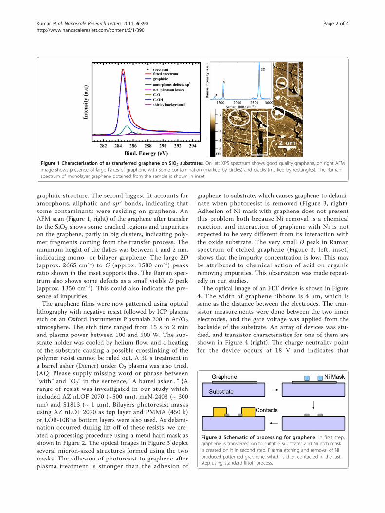
graphitic structure. The second biggest fit accounts foramorphous, aliphatic and sp3 bonds, indicating thatsome contaminants were residing on graphene. AnAFM scan (Figure 1, right) of the graphene after transferto the SiO2 shows some cracked regions and impuritieson the graphene, partly in big clusters, indicating poly-mer fragments coming from the transfer process. Theminimum height of the flakes was between 1 and 2 nm,indicating mono- or bilayer graphene. The large 2D(approx. 2665 cm-1) to G (approx. 1580 cm-1) peaksratio shown in the inset supports this. The Raman spec-trum also shows some defects as a small visible D peak(approx. 1350 cm-1). This could also indicate the pre-sence of impurities.The graphene films were now patterned using optical
lithography with negative resist followed by ICP plasmaetch on an Oxford Instruments Plasmalab 200 in Ar/O2
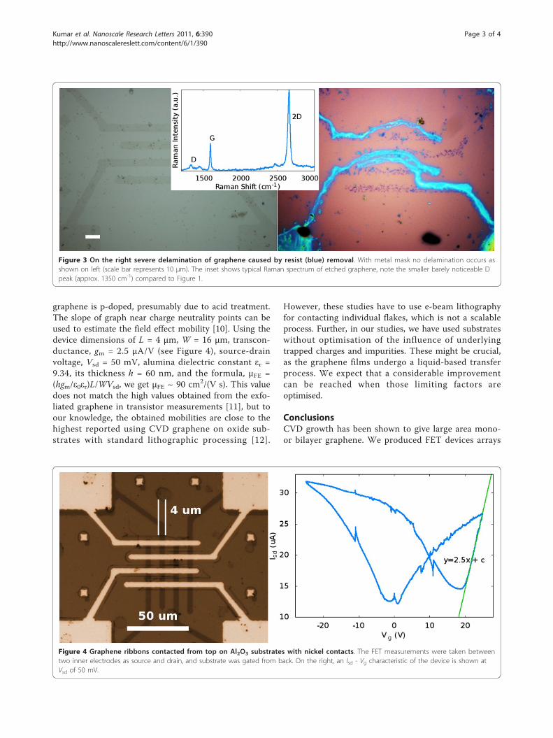
atmosphere. The etch time ranged from 15 s to 2 minand plasma power between 100 and 500 W. The sub-strate holder was cooled by helium flow, and a heatingof the substrate causing a possible crosslinking of thepolymer resist cannot be ruled out. A 30 s treatment ina barrel asher (Diener) under O2 plasma was also tried.{AQ: Please supply missing word or phrase between“with” and “O2“ in the sentence, “A barrel asher...” }Arange of resist was investigated in our study whichincluded AZ nLOF 2070 (~500 nm), maN-2403 (~ 300nm) and S1813 (~ 1 μm). Bilayers photoresist masksusing AZ nLOF 2070 as top layer and PMMA (450 k)or LOR-10B as bottom layers were also used. As delami-nation occurred during lift off of these resists, we cre-ated a processing procedure using a metal hard mask asshown in Figure 2. The optical images in Figure 3 depictseveral micron-sized structures formed using the twomasks. The adhesion of photoresist to graphene afterplasma treatment is stronger than the adhesion of
graphene to substrate, which causes graphene to delami-nate when photoresist is removed (Figure 3, right).Adhesion of Ni mask with graphene does not presentthis problem both because Ni removal is a chemicalreaction, and interaction of graphene with Ni is notexpected to be very different from its interaction withthe oxide substrate. The very small D peak in Ramanspectrum of etched graphene (Figure 3, left, inset)shows that the impurity concentration is low. This maybe attributed to chemical action of acid on organicremoving impurities. This observation was made repeat-edly in our studies.The optical image of an FET device is shown in Figure
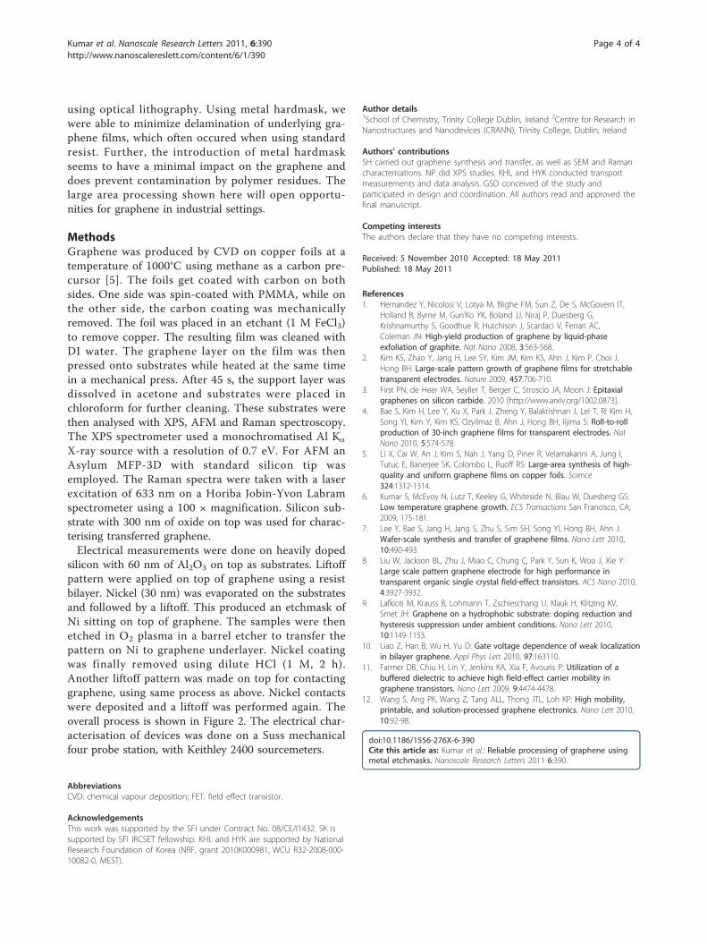
4. The width of graphene ribbons is 4 μm, which issame as the distance between the electrodes. The tran-sistor measurements were done between the two innerelectrodes, and the gate voltage was applied from thebackside of the substrate. An array of devices was stu-died, and transistor characteristics for one of them areshown in Figure 4 (right). The charge neutrality pointfor the device occurs at 18 V and indicates that
Figure 1 Characterisation of as transferred graphene on SiO2 substrates. On left XPS spectrum shows good quality graphene, on right AFMimage shows presence of large flakes of graphene with some contamination (marked by circles) and cracks (marked by rectangles). The Ramanspectrum of monolayer graphene obtained from the sample is shown in inset.
Figure 2 Schematic of processing for graphene. In first step,graphene is transferred on to suitable substrates and Ni etch maskis created on it in second step. Plasma etching and removal of Niproduced patterned graphene, which is then contacted in the laststep using standard liftoff process.
Kumar et al. Nanoscale Research Letters 2011, 6:390http://www.nanoscalereslett.com/content/6/1/390
Page 2 of 4
graphene is p-doped, presumably due to acid treatment.The slope of graph near charge neutrality points can beused to estimate the field effect mobility [10]. Using thedevice dimensions of L = 4 μm, W = 16 μm, transcon-ductance, gm = 2.5 μA/V (see Figure 4), source-drainvoltage, Vsd = 50 mV, alumina dielectric constant εr =9.34, its thickness h = 60 nm, and the formula, μFE =(hgm/ε0εr)L/WVsd, we get μFE ~ 90 cm2/(V s). This valuedoes not match the high values obtained from the exfo-liated graphene in transistor measurements [11], but toour knowledge, the obtained mobilities are close to thehighest reported using CVD graphene on oxide sub-strates with standard lithographic processing [12].
However, these studies have to use e-beam lithographyfor contacting individual flakes, which is not a scalableprocess. Further, in our studies, we have used substrateswithout optimisation of the influence of underlyingtrapped charges and impurities. These might be crucial,as the graphene films undergo a liquid-based transferprocess. We expect that a considerable improvementcan be reached when those limiting factors areoptimised.
ConclusionsCVD growth has been shown to give large area mono-or bilayer graphene. We produced FET devices arrays
Figure 3 On the right severe delamination of graphene caused by resist (blue) removal. With metal mask no delamination occurs asshown on left (scale bar represents 10 μm). The inset shows typical Raman spectrum of etched graphene, note the smaller barely noticeable Dpeak (approx. 1350 cm-1) compared to Figure 1.
Figure 4 Graphene ribbons contacted from top on Al2O3 substrates with nickel contacts. The FET measurements were taken betweentwo inner electrodes as source and drain, and substrate was gated from back. On the right, an Isd - Vg characteristic of the device is shown atVsd of 50 mV.
Kumar et al. Nanoscale Research Letters 2011, 6:390http://www.nanoscalereslett.com/content/6/1/390
Page 3 of 4
using optical lithography. Using metal hardmask, wewere able to minimize delamination of underlying gra-phene films, which often occured when using standardresist. Further, the introduction of metal hardmaskseems to have a minimal impact on the graphene anddoes prevent contamination by polymer residues. Thelarge area processing shown here will open opportu-nities for graphene in industrial settings.
MethodsGraphene was produced by CVD on copper foils at atemperature of 1000°C using methane as a carbon pre-cursor [5]. The foils get coated with carbon on bothsides. One side was spin-coated with PMMA, while onthe other side, the carbon coating was mechanicallyremoved. The foil was placed in an etchant (1 M FeCl3)to remove copper. The resulting film was cleaned withDI water. The graphene layer on the film was thenpressed onto substrates while heated at the same timein a mechanical press. After 45 s, the support layer wasdissolved in acetone and substrates were placed inchloroform for further cleaning. These substrates werethen analysed with XPS, AFM and Raman spectroscopy.The XPS spectrometer used a monochromatised Al Ka
X-ray source with a resolution of 0.7 eV. For AFM anAsylum MFP-3D with standard silicon tip wasemployed. The Raman spectra were taken with a laserexcitation of 633 nm on a Horiba Jobin-Yvon Labramspectrometer using a 100 × magnification. Silicon sub-strate with 300 nm of oxide on top was used for charac-terising transferred graphene.Electrical measurements were done on heavily doped
silicon with 60 nm of Al2O3 on top as substrates. Liftoffpattern were applied on top of graphene using a resistbilayer. Nickel (30 nm) was evaporated on the substratesand followed by a liftoff. This produced an etchmask ofNi sitting on top of graphene. The samples were thenetched in O2 plasma in a barrel etcher to transfer thepattern on Ni to graphene underlayer. Nickel coatingwas finally removed using dilute HCl (1 M, 2 h).Another liftoff pattern was made on top for contactinggraphene, using same process as above. Nickel contactswere deposited and a liftoff was performed again. Theoverall process is shown in Figure 2. The electrical char-acterisation of devices was done on a Suss mechanicalfour probe station, with Keithley 2400 sourcemeters.
AbbreviationsCVD: chemical vapour deposition; FET: field effect transistor.
AcknowledgementsThis work was supported by the SFI under Contract No. 08/CE/I1432. SK issupported by SFI IRCSET fellowship. KHL and HYK are supported by NationalResearch Foundation of Korea (NRF, grant 2010K000981, WCU R32-2008-000-10082-0, MEST).
Author details1School of Chemistry, Trinity College Dublin, Ireland 2Centre for Research inNanostructures and Nanodevices (CRANN), Trinity College, Dublin, Ireland
Authors’ contributionsSH carried out graphene synthesis and transfer, as well as SEM and Ramancharacterisations. NP did XPS studies. KHL and HYK conducted transportmeasurements and data analysis. GSD conceived of the study andparticipated in design and coordination. All authors read and approved thefinal manuscript.
Competing interestsThe authors declare that they have no competing interests.
Received: 5 November 2010 Accepted: 18 May 2011Published: 18 May 2011
References1. Hernandez Y, Nicolosi V, Lotya M, Blighe FM, Sun Z, De S, McGovern IT,
Holland B, Byrne M, Gun’Ko YK, Boland JJ, Niraj P, Duesberg G,Krishnamurthy S, Goodhue R, Hutchison J, Scardaci V, Ferrari AC,Coleman JN: High-yield production of graphene by liquid-phaseexfoliation of graphite. Nat Nano 2008, 3:563-568.
2. Kim KS, Zhao Y, Jang H, Lee SY, Kim JM, Kim KS, Ahn J, Kim P, Choi J,Hong BH: Large-scale pattern growth of graphene films for stretchabletransparent electrodes. Nature 2009, 457:706-710.
3. First PN, de Heer WA, Seyller T, Berger C, Stroscio JA, Moon J: Epitaxialgraphenes on silicon carbide. 2010 [http://www.arxiv.org/1002.0873].
4. Bae S, Kim H, Lee Y, Xu X, Park J, Zheng Y, Balakrishnan J, Lei T, Ri Kim H,Song YI, Kim Y, Kim KS, Ozyilmaz B, Ahn J, Hong BH, Iijima S: Roll-to-rollproduction of 30-inch graphene films for transparent electrodes. NatNano 2010, 5:574-578.
5. Li X, Cai W, An J, Kim S, Nah J, Yang D, Piner R, Velamakanni A, Jung I,Tutuc E, Banerjee SK, Colombo L, Ruoff RS: Large-area synthesis of high-quality and uniform graphene films on copper foils. Science324:1312-1314.
6. Kumar S, McEvoy N, Lutz T, Keeley G, Whiteside N, Blau W, Duesberg GS:Low temperature graphene growth. ECS Transactions San Francisco, CA;2009, 175-181.
7. Lee Y, Bae S, Jang H, Jang S, Zhu S, Sim SH, Song YI, Hong BH, Ahn J:Wafer-scale synthesis and transfer of graphene films. Nano Lett 2010,10:490-493.
8. Liu W, Jackson BL, Zhu J, Miao C, Chung C, Park Y, Sun K, Woo J, Xie Y:Large scale pattern graphene electrode for high performance intransparent organic single crystal field-effect transistors. ACS Nano 2010,4:3927-3932.
9. Lafkioti M, Krauss B, Lohmann T, Zschieschang U, Klauk H, Klitzing KV,Smet JH: Graphene on a hydrophobic substrate: doping reduction andhysteresis suppression under ambient conditions. Nano Lett 2010,10:1149-1153.
10. Liao Z, Han B, Wu H, Yu D: Gate voltage dependence of weak localizationin bilayer graphene. Appl Phys Lett 2010, 97:163110.
11. Farmer DB, Chiu H, Lin Y, Jenkins KA, Xia F, Avouris P: Utilization of abuffered dielectric to achieve high field-effect carrier mobility ingraphene transistors. Nano Lett 2009, 9:4474-4478.
12. Wang S, Ang PK, Wang Z, Tang ALL, Thong JTL, Loh KP: High mobility,printable, and solution-processed graphene electronics. Nano Lett 2010,10:92-98.
doi:10.1186/1556-276X-6-390Cite this article as: Kumar et al.: Reliable processing of graphene usingmetal etchmasks. Nanoscale Research Letters 2011 6:390.
Kumar et al. Nanoscale Research Letters 2011, 6:390http://www.nanoscalereslett.com/content/6/1/390
Page 4 of 4