Embed Size (px)
Citation preview
Liu et al. Nanoscale Research Letters 2012, 7:318http://www.nanoscalereslett.com/content/7/1/318
NANO EXPRESS Open Access
Laser etching of groove structures withmicro-optical fiber-enhanced irradiationDameng Liu*, Jiachen Liu, Hui Wang and Tianmin Shao
Abstract
A microfiber is used as a laser-focusing unit to fabricate a groove structure on TiAlSiN surfaces. After one laser pulseetching, a groove with the minimum width of 265 nm is manufactured at the area. This technique ofmicrofabricating the groove in microscale is studied. Based on the near-field intensity enhancement at the contactarea between the fiber and the surface during the laser irradiation, simulation results are also presented, whichagree well with the experimental results.
Keywords: Micro-fiber, Laser, Micro-fabrication
BackgroundIn the past 10 years, with the important role of microde-vices in industrial applications, fabrication technologies onthe micron and nanometer scales are attracting more atten-tions. Recently, developed lithographic technologies like ionbeam, electron beam, and near-field optics have been inves-tigated and regarded as potential methods for microfabrica-tion [1-4]. Due to the light diffraction limit, traditional laseroptical manufacture is not available to fabricate the furthermicrosturctures [5]. Many groups offered approaches toovercome the limit by using near-field effects through sur-face pattern designs. These are carried out by delivering alaser beam through a near-field tip or illuminating the tipwith a pulsed laser. Huang et al. used single-pulse 248 nmKrF laser radiation to fabricate nano bump arrays [6]. Honget al. reported that femtosecond laser (400 nm, 100 fs)irradiation went through a near-field scanning opticalmicroscope and sub-50 nm feature size was created [7].The near-field enhanced laser irradiation with 248 and 355nm UV lasers was applied to pattern a silicon surface in amassively parallel fashion [8]. However, these approachesneed the expensive equipment with the related complexsystem. Zhang et al. used a 248 nm excimer laser with apulse duration of 23 ns and obtained 100 nm hillocks at theoriginal particle positions [4]. These glass microballs canonly be used for processing micro-dimple structures. Zhouet al. also tried a low-cost method, in which an optical fiberwas used as a focusing unit to etch parallel microgrooves
* Correspondence: [email protected] Key Laboratory of Tribology, Tsinghua University, Beijing 100084, China
© 2012 LIU et al.;licensee BioMed Central Ltd. TCommons Attribution License (http://creativecoreproduction in any medium, provided the orig
with 2 to 6 μm width and 0.7 to 1.4 μm depth on Si surface[9]. This resolution still needed to be improved to over-come the diffraction limit. Meanwhile, it is necessary forthe micro and nanofabrication to develop the low-cost andfast speed laser processing [10]. To further reduce the reso-lution to the nanometer scale, methods of near-field laserirradiation with the combination of advanced processingtools such as SPM, NSOM, transparent, and metallic parti-cles are applied for the sizes as small as 20 nm. Laser inter-ference lithography is also capable of fabricating sub-100nm periodic structures for large area, maskless, and non-contact nanofabrications [7]. In this work, we report a low-cost microprocessing technique, based on a microfiber-enhanced irradiation to fabricate groove structures underthe diffraction limit.
MethodsA laser etching experiment with the microfiber-enhancedirradiation is designed to fabricate a groove on TiAlSiN sur-faces (Figure 1). Nd: YAG solid state laser at a wavelengthof 1.06 μm, repetitive rate of 1 to 10 Hz, and laser beamdiameter of 7 mm is applied in our experiment as a lightsource. This fiber was fabricated from a quartz optical fiber.The original fiber's diameter is 125 μm, with the refractiveindex of 1.588. The ultrasound process is used for thequartz fiber in order to remove its plastic covers in sulfuricacid. Then, the fiber is washed in DI water and dipped intohydrofluoric acid solution (47%) for about 50 min. Finally, afiber in microscale is obtained and examined under a highresolution scanning electron microscope (SEM).
his is an Open Access article distributed under the terms of the Creativemmons.org/licenses/by/2.0), which permits unrestricted use, distribution, andinal work is properly cited.
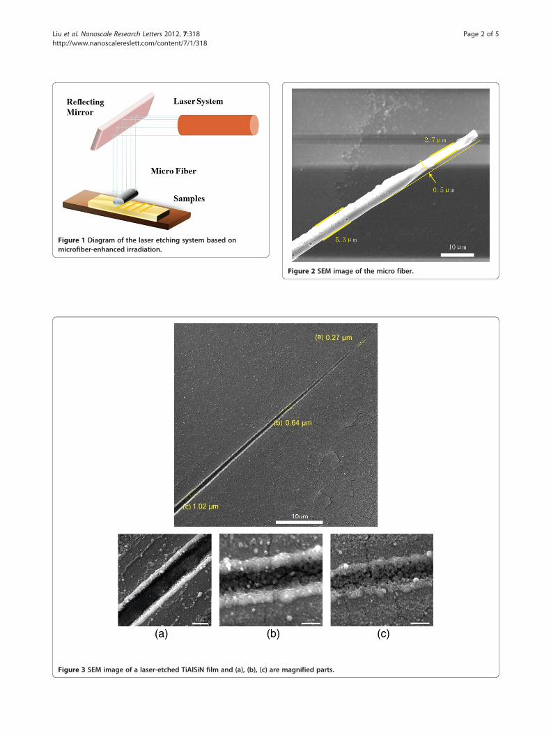
Figure 1 Diagram of the laser etching system based onmicrofiber-enhanced irradiation.
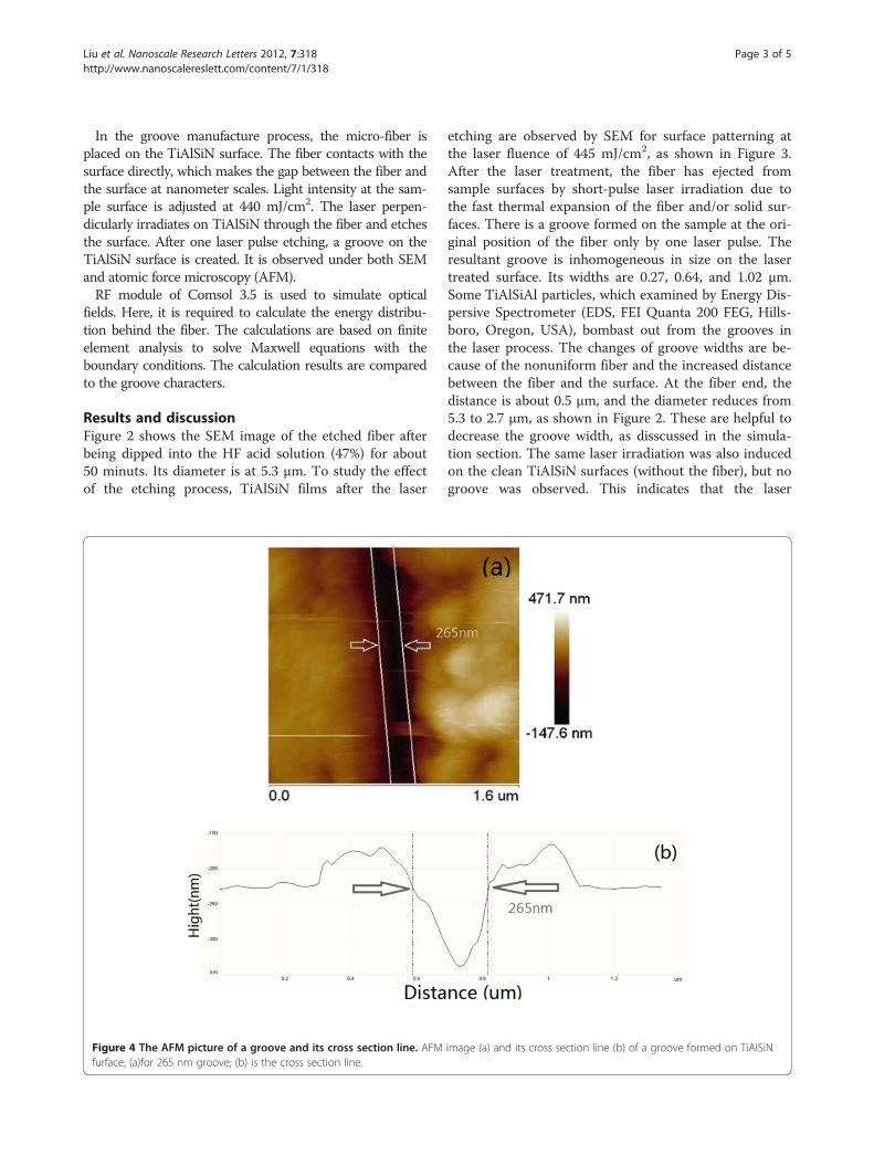
Figure 2 SEM image of the micro fiber.
(a) (b) (c)
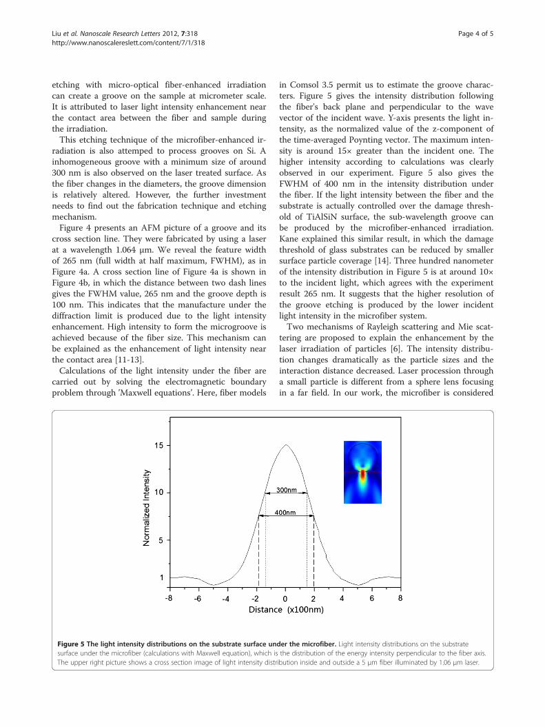
Figure 3 SEM image of a laser-etched TiAlSiN film and (a), (b), (c) are magnified parts.
Liu et al. Nanoscale Research Letters 2012, 7:318 Page 2 of 5http://www.nanoscalereslett.com/content/7/1/318
Liu et al. Nanoscale Research Letters 2012, 7:318 Page 3 of 5http://www.nanoscalereslett.com/content/7/1/318
In the groove manufacture process, the micro-fiber isplaced on the TiAlSiN surface. The fiber contacts with thesurface directly, which makes the gap between the fiber andthe surface at nanometer scales. Light intensity at the sam-ple surface is adjusted at 440 mJ/cm2. The laser perpen-dicularly irradiates on TiAlSiN through the fiber and etchesthe surface. After one laser pulse etching, a groove on theTiAlSiN surface is created. It is observed under both SEMand atomic force microscopy (AFM).RF module of Comsol 3.5 is used to simulate optical
fields. Here, it is required to calculate the energy distribu-tion behind the fiber. The calculations are based on finiteelement analysis to solve Maxwell equations with theboundary conditions. The calculation results are comparedto the groove characters.
Results and discussionFigure 2 shows the SEM image of the etched fiber afterbeing dipped into the HF acid solution (47%) for about50 minuts. Its diameter is at 5.3 μm. To study the effectof the etching process, TiAlSiN films after the laser
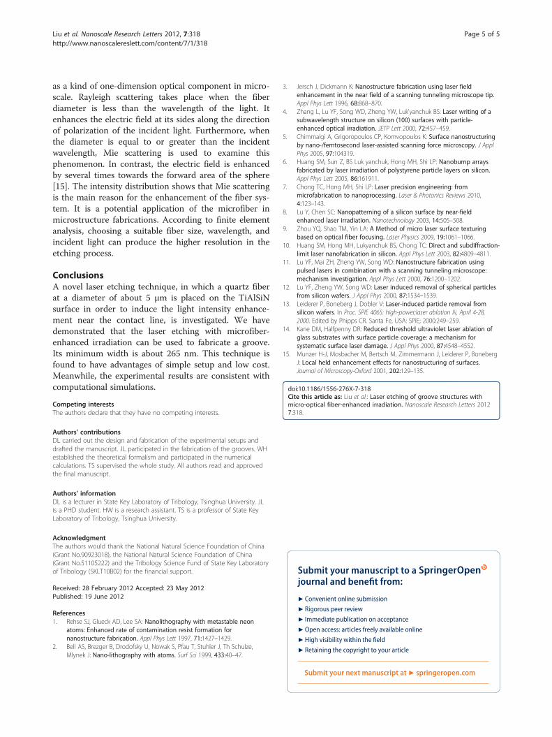
Figure 4 The AFM picture of a groove and its cross section line. AFMfurface, (a)for 265 nm groove; (b) is the cross section line.
etching are observed by SEM for surface patterning atthe laser fluence of 445 mJ/cm2, as shown in Figure 3.After the laser treatment, the fiber has ejected fromsample surfaces by short-pulse laser irradiation due tothe fast thermal expansion of the fiber and/or solid sur-faces. There is a groove formed on the sample at the ori-ginal position of the fiber only by one laser pulse. Theresultant groove is inhomogeneous in size on the lasertreated surface. Its widths are 0.27, 0.64, and 1.02 μm.Some TiAlSiAl particles, which examined by Energy Dis-persive Spectrometer (EDS, FEI Quanta 200 FEG, Hills-boro, Oregon, USA), bombast out from the grooves inthe laser process. The changes of groove widths are be-cause of the nonuniform fiber and the increased distancebetween the fiber and the surface. At the fiber end, thedistance is about 0.5 μm, and the diameter reduces from5.3 to 2.7 μm, as shown in Figure 2. These are helpful todecrease the groove width, as disscussed in the simula-tion section. The same laser irradiation was also inducedon the clean TiAlSiN surfaces (without the fiber), but nogroove was observed. This indicates that the laser
image (a) and its cross section line (b) of a groove formed on TiAlSiN
Liu et al. Nanoscale Research Letters 2012, 7:318 Page 4 of 5http://www.nanoscalereslett.com/content/7/1/318
etching with micro-optical fiber-enhanced irradiationcan create a groove on the sample at micrometer scale.It is attributed to laser light intensity enhancement nearthe contact area between the fiber and sample duringthe irradiation.This etching technique of the microfiber-enhanced ir-
radiation is also attemped to process grooves on Si. Ainhomogeneous groove with a minimum size of around300 nm is also observed on the laser treated surface. Asthe fiber changes in the diameters, the groove dimensionis relatively altered. However, the further investmentneeds to find out the fabrication technique and etchingmechanism.Figure 4 presents an AFM picture of a groove and its
cross section line. They were fabricated by using a laserat a wavelength 1.064 μm. We reveal the feature widthof 265 nm (full width at half maximum, FWHM), as inFigure 4a. A cross section line of Figure 4a is shown inFigure 4b, in which the distance between two dash linesgives the FWHM value, 265 nm and the groove depth is100 nm. This indicates that the manufacture under thediffraction limit is produced due to the light intensityenhancement. High intensity to form the microgroove isachieved because of the fiber size. This mechanism canbe explained as the enhancement of light intensity nearthe contact area [11-13].Calculations of the light intensity under the fiber are
carried out by solving the electromagnetic boundaryproblem through ’Maxwell equations’. Here, fiber models
Figure 5 The light intensity distributions on the substrate surface undsurface under the microfiber (calculations with Maxwell equation), which isThe upper right picture shows a cross section image of light intensity distr
in Comsol 3.5 permit us to estimate the groove charac-ters. Figure 5 gives the intensity distribution followingthe fiber's back plane and perpendicular to the wavevector of the incident wave. Y-axis presents the light in-tensity, as the normalized value of the z-component ofthe time-averaged Poynting vector. The maximum inten-sity is around 15× greater than the incident one. Thehigher intensity according to calculations was clearlyobserved in our experiment. Figure 5 also gives theFWHM of 400 nm in the intensity distribution underthe fiber. If the light intensity between the fiber and thesubstrate is actually controlled over the damage thresh-old of TiAlSiN surface, the sub-wavelength groove canbe produced by the microfiber-enhanced irradiation.Kane explained this similar result, in which the damagethreshold of glass substrates can be reduced by smallersurface particle coverage [14]. Three hundred nanometerof the intensity distribution in Figure 5 is at around 10×to the incident light, which agrees with the experimentresult 265 nm. It suggests that the higher resolution ofthe groove etching is produced by the lower incidentlight intensity in the microfiber system.Two mechanisms of Rayleigh scattering and Mie scat-
tering are proposed to explain the enhancement by thelaser irradiation of particles [6]. The intensity distribu-tion changes dramatically as the particle sizes and theinteraction distance decreased. Laser procession througha small particle is different from a sphere lens focusingin a far field. In our work, the microfiber is considered
er the microfiber. Light intensity distributions on the substratethe distribution of the energy intensity perpendicular to the fiber axis.ibution inside and outside a 5 μm fiber illuminated by 1.06 μm laser.
Liu et al. Nanoscale Research Letters 2012, 7:318 Page 5 of 5http://www.nanoscalereslett.com/content/7/1/318
as a kind of one-dimension optical component in micro-scale. Rayleigh scattering takes place when the fiberdiameter is less than the wavelength of the light. Itenhances the electric field at its sides along the directionof polarization of the incident light. Furthermore, whenthe diameter is equal to or greater than the incidentwavelength, Mie scattering is used to examine thisphenomenon. In contrast, the electric field is enhancedby several times towards the forward area of the sphere[15]. The intensity distribution shows that Mie scatteringis the main reason for the enhancement of the fiber sys-tem. It is a potential application of the microfiber inmicrostructure fabrications. According to finite elementanalysis, choosing a suitable fiber size, wavelength, andincident light can produce the higher resolution in theetching process.
ConclusionsA novel laser etching technique, in which a quartz fiberat a diameter of about 5 μm is placed on the TiAlSiNsurface in order to induce the light intensity enhance-ment near the contact line, is investigated. We havedemonstrated that the laser etching with microfiber-enhanced irradiation can be used to fabricate a groove.Its minimum width is about 265 nm. This technique isfound to have advantages of simple setup and low cost.Meanwhile, the experimental results are consistent withcomputational simulations.
Competing interestsThe authors declare that they have no competing interests.
Authors’ contributionsDL carried out the design and fabrication of the experimental setups anddrafted the manuscript. JL participated in the fabrication of the grooves. WHestablished the theoretical formalism and participated in the numericalcalculations. TS supervised the whole study. All authors read and approvedthe final manuscript.
Authors’ informationDL is a lecturer in State Key Laboratory of Tribology, Tsinghua University. JLis a PHD student. HW is a research assistant. TS is a professor of State KeyLaboratory of Tribology, Tsinghua University.
AcknowledgmentThe authors would thank the National Natural Science Foundation of China(Grant No.90923018), the National Natural Science Foundation of China(Grant No.51105222) and the Tribology Science Fund of State Key Laboratoryof Tribology (SKLT10B02) for the financial support.
Received: 28 February 2012 Accepted: 23 May 2012Published: 19 June 2012
References1. Rehse SJ, Glueck AD, Lee SA: Nanolithography with metastable neon
atoms: Enhanced rate of contamination resist formation fornanostructure fabrication. Appl Phys Lett 1997, 71:1427–1429.
2. Bell AS, Brezger B, Drodofsky U, Nowak S, Pfau T, Stuhler J, Th Schulze,Mlynek J: Nano-lithography with atoms. Surf Sci 1999, 433:40–47.
3. Jersch J, Dickmann K: Nanostructure fabrication using laser fieldenhancement in the near field of a scanning tunneling microscope tip.Appl Phys Lett 1996, 68:868–870.
4. Zhang L, Lu YF, Song WD, Zheng YW, Luk'yanchuk BS: Laser writing of asubwavelength structure on silicon (100) surfaces with particle-enhanced optical irradiation. JETP Lett 2000, 72:457–459.
5. Chimmalgi A, Grigoropoulos CP, Komvopoulos K: Surface nanostructuringby nano-/femtosecond laser-assisted scanning force microscopy. J ApplPhys 2005, 97:104319.
6. Huang SM, Sun Z, BS Luk yanchuk, Hong MH, Shi LP: Nanobump arraysfabricated by laser irradiation of polystyrene particle layers on silicon.Appl Phys Lett 2005, 86:161911.
7. Chong TC, Hong MH, Shi LP: Laser precision engineering: frommicrofabrication to nanoprocessing. Laser & Photonics Reviews 2010,4:123–143.
8. Lu Y, Chen SC: Nanopatterning of a silicon surface by near-fieldenhanced laser irradiation. Nanotechnology 2003, 14:505–508.
9. Zhou YQ, Shao TM, Yin LA: A Method of micro laser surface texturingbased on optical fiber focusing. Laser Physics 2009, 19:1061–1066.
10. Huang SM, Hong MH, Lukyanchuk BS, Chong TC: Direct and subdiffraction-limit laser nanofabrication in silicon. Appl Phys Lett 2003, 82:4809–4811.
11. Lu YF, Mai ZH, Zheng YW, Song WD: Nanostructure fabrication usingpulsed lasers in combination with a scanning tunneling microscope:mechanism investigation. Appl Phys Lett 2000, 76:1200–1202.
12. Lu YF, Zheng YW, Song WD: Laser induced removal of spherical particlesfrom silicon wafers. J Appl Phys 2000, 87:1534–1539.
13. Leiderer P, Boneberg J, Dobler V: Laser-induced particle removal fromsilicon wafers. In Proc. SPIE 4065: high-power;laser ablation Iii, April 4-28,2000. Edited by Phipps CR. Santa Fe, USA: SPIE; 2000:249–259.
14. Kane DM, Halfpenny DR: Reduced threshold ultraviolet laser ablation ofglass substrates with surface particle coverage: a mechanism forsystematic surface laser damage. J Appl Phys 2000, 87:4548–4552.
15. Munzer H-J, Mosbacher M, Bertsch M, Zimmermann J, Leiderer P, BonebergJ: Local held enhancement effects for nanostructuring of surfaces.Journal of Microscopy-Oxford 2001, 202:129–135.
doi:10.1186/1556-276X-7-318Cite this article as: Liu et al.: Laser etching of groove structures withmicro-optical fiber-enhanced irradiation. Nanoscale Research Letters 20127:318.
Submit your manuscript to a journal and benefi t from:
7 Convenient online submission
7 Rigorous peer review
7 Immediate publication on acceptance
7 Open access: articles freely available online
7 High visibility within the fi eld
7 Retaining the copyright to your article
Submit your next manuscript at 7 springeropen.com


![FIB Secondary Etching Method for Fabrication of Fine CNT ... · laser etching method was utilized to obtain microstructures of CNT brushes [21]. Moreover, the patterned growth of](https://img.pdfslide.us/doc/110x75/5e7104f042569253791c508c/fib-secondary-etching-method-for-fabrication-of-fine-cnt-laser-etching-method.jpg)