Embed Size (px)
Citation preview

Jana et al. Nanoscale Research Letters 2014, 9:12http://www.nanoscalereslett.com/content/9/1/12
NANO EXPRESS Open Access
Enhanced resistive switching phenomena usinglow-positive-voltage format and self-complianceIrOx/GdOx/W cross-point memoriesDebanjan Jana1, Siddheswar Maikap1*, Amit Prakash1, Yi-Yan Chen2, Hsien-Chin Chiu1 and Jer-Ren Yang2
Abstract
Enhanced resistive switching phenomena of IrOx/GdOx/W cross-point memory devices have been observed ascompared to the via-hole devices. The as-deposited Gd2O3 films with a thickness of approximately 15 nm showpolycrystalline that is observed using high-resolution transmission electron microscope. Via-hole memory deviceshows bipolar resistive switching phenomena with a large formation voltage of −6.4 V and high operation currentof >1 mA, while the cross-point memory device shows also bipolar resistive switching with low-voltage format of+2 V and self-compliance operation current of <300 μA. Switching mechanism is based on the formation andrupture of conducting filament at the IrOx/GdOx interface, owing to oxygen ion migration. The oxygen-rich GdOx
layer formation at the IrOx/GdOx interface will also help control the resistive switching characteristics. Thiscross-point memory device has also Repeatable 100 DC switching cycles, narrow distribution of LRS/HRS, excellentpulse endurance of >10,000 in every cycle, and good data retention of >104 s. This memory device has greatpotential for future nanoscale high-density non-volatile memory applications.
Keywords: RRAM; GdOx; Self-compliance; Resistive switching
BackgroundThere is an increasing demand for next-generation high-density non-volatile memory devices because flash mem-ories are approaching their scaling limits. Among manycandidates to replace the flash memory devices, resistiverandom access memory (RRAM) is one of the promisingcandidates, owing to its simple metal-insulator-metalstructure, fast switching speed, low-power operation, ex-cellent scalability potential, and high density in crossbarstructure [1-4]. Many switching materials such as TaOx
[5-7], AlOx [8,9], HfOx [10-15], TiOx [16,17], NiOx
[18-21], WOx [22,23], ZnOx [24,25], ZrOx [26-31],SrTiO3 [32,33], SiOx [34,35], and Pr0.7Ca0.3MnO3 [36,37]have been studied by several groups. However, the rare-earth oxide such as Gd2O3 could be a promising resistiveswitching material because of its high resistivity, highdielectric permittivity (κ = 16), moderate energy gap
* Correspondence: [email protected] Film Nano Technology Laboratory, Department of ElectronicEngineering, Chang Gung University, 259 Wen-Hwa 1st Rd, Kwei-Shan,Tao-Yuan 333, TaiwanFull list of author information is available at the end of the article
© 2014 Jana et al.; licensee Springer. This is anAttribution License (http://creativecommons.orin any medium, provided the original work is p
(Eg = approximately 5.3 eV), and higher thermodynamicstability [38]. Recently, many researchers have reported theresistive switching properties by using Gd2O3 materials[38-40]. Cao et al. [38] have reported unipolar resistiveswitching phenomena using Pt/Gd2O3/Pt structure witha high RESET current of 35 mA. Liu et al. [39] havealso reported unipolar resistive switching phenomenawith a high RESET current of 10 mA in Ti/Gd2O3/Ptstructure. Yoon et al. [40] have reported resistiveswitching characteristics using MoOx/GdOx bilayerstructure with a RESET current of 300 μA. It is foundthat non-uniform switching and high overshoot currentare the main drawbacks for practical application ofnon-volatile RRAM using Gd2O3 material. Even thoughmany structures using the Gd2O3 materials have beenreported, however, the cross-point memory devicesusing IrOx/GdOx/W structure have not yet been re-ported. It is reported [41] that the cross-point structurehas a great potential for high-density memory applica-tion in the near future.In this study, we discussed resistive switching phe-
nomena of IrOx/GdOx/W cross-point memory structure.
Open Access article distributed under the terms of the Creative Commonsg/licenses/by/2.0), which permits unrestricted use, distribution, and reproductionroperly cited.

Figure 1 Schematic view of IrOx/GdOx/W cross-point memorydevice. Positive bias is applied at the TE, and BE was groundedduring the measurement.
Jana et al. Nanoscale Research Letters 2014, 9:12 Page 2 of 8http://www.nanoscalereslett.com/content/9/1/12
For comparison, the IrOx/GdOx/W via-hole structurehas been also investigated. The IrOx/GdOx/W via-holememory devices exhibit negative switching polarity,whereas the IrOx/GdOx/W cross-point memory de-vices show positive switching polarity. Switching non-uniformity and high operation voltage/current of thevia-hole devices are observed. To improve the switchinguniformity and control the current overshoot, we havedesigned the IrOx/GdOx/W cross-point memory devices.In the cross-point structure, IrOx/GdOx/W memory de-vice shows stable and uniform positive switching due tothe formation of oxygen-rich interfacial layer at theIrOx/GdOx interface. The cross-point memory devicehas self-compliance bipolar resistive switching phenom-ena of consecutive 100 cycles with narrow distributionof high resistance state (HRS), low resistance state(LRS), good device-to-device uniformity, excellent P/Ecycles of >10,000, and good data retention with resist-ance ratio of 100 after 104 s under a low operation volt-age of ±3.5 V.
MethodsFirst, the cross-point memory devices using the IrOx/GdOx/W structure were fabricated. After conventionalRCA cleaning of p-type Si wafer, 200-nm-thick SiO2 wasgrown by wet oxidation process. Then, a tungsten (W)metal layer of approximately 200 nm was deposited onthe SiO2/Si substrate by radio frequency (rf ) sputteringprocess. The deposition power was 150 W, and argon(Ar) with flow rate of 25 sccm was used. The W barswith different widths of 4 to 50 μm were patterned byoptical lithography and wet etching process, which serveas bottom electrode (BE). Another lithography processstep was used to obtain top electrode bar (TE) by lift-off.The high-κ Gd2O3 as a switching material was depositedby electron beam evaporation. The thickness of theGd2O3 film was approximately 15 nm. Pure Gd2O3 shotswith granules sizes of 2 to 3 mm were used. The depos-ition rate of Gd2O3 was 0.2 Å/s, and the power was400 W. Then, iridium-oxide (IrOx) as a TE with a thick-ness of approximately 200 nm was deposited by rf sput-tering. An iridium (Ir) target was used for the IrOx TE.The ratio of Ar to O gases was 1:1 (i.e., 25/25 sccm).The deposition power and chamber pressure were 50 Wand 20 mTorr, respectively. The Ir bars with differentwidths of 4 to 50 μm were laid 90° with W BEs. Finally,lift-off was performed to get the final devices with differ-ent sizes of 4 × 4 to 50 × 50 μm2. Then, the device wasannealed at 400°C in N2 ambient for 10 min. The N2
pressure was 5 SLM. The cross-point memories with dif-ferent arrays of 1 × 1 to 10 × 10 were designed, and thememory device at the 1 × 1 position was measured inthis study. Figure 1 shows a schematic view of our IrOx/GdOx/W cross-point memory device. Figure 2 shows the
topography of the Gd2O3 and IrOx films, observed usingatomic force microscope (AFM). AFM images of two-dimensional (2D) format are shown in Figure 2a,c, andthree-dimensional (3D) images are shown in Figure 2b,d.The root mean square (rms, Rq) and average (Ra) surfaceroughness are found to be 0.688 and 0.518 nm of theGd2O3 film on Si substrate, while those values are foundto be 1.29 and 1.03 nm of the IrOx film on Gd2O3/SiO2/Si substrate, respectively. For comparison, we have alsostudied the surface roughness of W BE for the via-holeand cross-point memory devices. The root mean square(Rq) surface roughness of W BE for the via-hole andcross-point devices is found to be 1.35 and 4.21 nm, andthe average surface roughness (Ra) is found to be 1.05and 3.35 nm, respectively [42]. It is observed that thesurface roughness of W BE is higher than those of GdOx
and IrOx, which might have great impact on W BE aswell as improved resistive switching characteristics.Second, the via-hole devices were fabricated for com-
parison. The fabrication steps are as follows. The Wmetal as a BE was deposited by rf sputtering on SiO2
(200 nm)/Si wafers. In this device, the thickness of Wlayer was approximately 100 nm. To form the RRAMdevice, the SiO2 layer with a thickness of approximately150 nm was deposited. Then, a small via-hole with anactive area of 2 × 2 μm2 was designed using standardlithography. Photoresist (PR) was used to design the pat-tern and was opened at the active and TE regions. Then,the Gd2O3 film with a thickness of 15 nm was deposited.Finally, lift-off was performed to get the memory device.A schematic view of our IrOx/GdOx/W via-hole struc-ture is shown in Figure 3. During electrical measurementof the memory devices, the BE was grounded and thesweeping bias was applied on the TE.
Results and discussionFigure 4a shows the HRTEM image of our memory de-vice for the as-deposited Gd2O3 film. Each layer isshown. The thickness of the GdOx layer is approximately15 nm. To identify the crystalline nature of the Gd2O3

Figure 2 AFM images of the films. GdOx film on SiO2/Si substrate in (a) 2D and (b) 3D views. IrOx film on IrOx/GdOx/SiO2/Si stack in (c) 2D and(d) 3D views.
Jana et al. Nanoscale Research Letters 2014, 9:12 Page 3 of 8http://www.nanoscalereslett.com/content/9/1/12
film, the calculated d spacings are found to be 2.78 Å(101), 2.91 Å (002), and 3.06 Å (100), which are similar(2.69 Å (200), 3.09 Å (111), and 1.89 Å (220)) to thosereported in the literature [43]. This suggests that thisas-deposited Gd2O3 film is polycrystalline. The energydiffraction X-ray spectroscopy (EDX) spectra confirm
Figure 3 Schematic view of resistive switching memory devicein an IrOx/GdOx/W via-hole structure. Typical device sizeis 2 × 2 μm2.
the presence of expected elements Ir, Gd, W, and O inrespective layers, as shown in Figure 4b. The X-rayphotoelectron spectroscopy (XPS) spectra of Gd 3d5/2and Gd2O3 3d5/2 peaks are located at 1,186.73 and1,189 eV, respectively (Figure 5), which proves a Gd-richGd2O3 film, i.e., GdOx. The height ratio of Gd/Gd2O3 is1:0.93, and area ratio of Gd/Gd2O3 is 1:0.89. Arhen et al.[44] reported the same chemical bonding states at 1,186and 1,188 eV for the Gd 3d5/2 and Gd2O3 3d5/2 peaks,respectively. This suggests that the as-deposited Gd2O3
film is a Gd-rich GdOx film. It is known that the grainboundary has more defects or weak Gd-O bonds. Thissuggests that the Gd-O bonds will break easily under ex-ternal bias, and more oxygen vacancies will be created.The conducting filament will be formed through thegrain boundaries. However, the nanotips on the W BEwill help the structure have repeatable resistive switchingmemory characteristics.Figure 6a shows the typical current–voltage (I-V) char-
acteristics of a IrOx/GdOx/W RRAM device in via-holestructure, as illustrated schematically in Figure 3. Thepristine device shows very low leakage current (arrow 1).In order to activate the resistive switching, an initial softbreakdown process (forming) was carried out by apply-ing negative bias on the TE. The negative forming volt-age (Vform) is −6.4 V to initiate the resistive switching
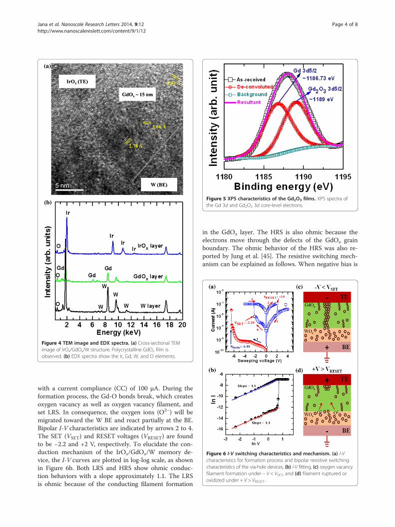
Figure 4 TEM image and EDX spectra. (a) Cross-sectional TEMimage of IrOx/GdOx/W structure. Polycrystalline GdOx film isobserved. (b) EDX spectra show the Ir, Gd, W, and O elements.
Figure 5 XPS characteristics of the Gd2O3 films. XPS spectra ofthe Gd 3d and Gd2O3 3d core-level electrons.
Figure 6 I-V switching characteristics and mechanism. (a) I-Vcharacteristics for formation process and bipolar resistive switchingcharacteristics of the via-hole devices, (b) I-V fitting, (c) oxygen vacancyfilament formation under − V < VSET, and (d) filament ruptured oroxidized under + V > VRESET.
Jana et al. Nanoscale Research Letters 2014, 9:12 Page 4 of 8http://www.nanoscalereslett.com/content/9/1/12
with a current compliance (CC) of 100 μA. During theformation process, the Gd-O bonds break, which createsoxygen vacancy as well as oxygen vacancy filament, andset LRS. In consequence, the oxygen ions (O2–) will bemigrated toward the W BE and react partially at the BE.Bipolar I-V characteristics are indicated by arrows 2 to 4.The SET (VSET) and RESET voltages (VRESET) are foundto be −2.2 and +2 V, respectively. To elucidate the con-duction mechanism of the IrOx/GdOx/W memory de-vice, the I-V curves are plotted in log-log scale, as shownin Figure 6b. Both LRS and HRS show ohmic conduc-tion behaviors with a slope approximately 1.1. The LRSis ohmic because of the conducting filament formation
in the GdOx layer. The HRS is also ohmic because theelectrons move through the defects of the GdOx grainboundary. The ohmic behavior of the HRS was also re-ported by Jung et al. [45]. The resistive switching mech-anism can be explained as follows. When negative bias is
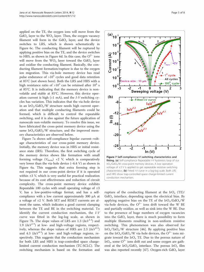
Figure 7 Self-compliance I-V switching characteristics andfitting. (a) Self-compliance Repeatable I-V hysteresis loop of ourIrOx/GdOx/W cross-point memory devices. A low operationvoltage of ±3 V is applied to get repeatable resistive switchingcharacteristics. (b) Fitted I-V curve in a log-log scale. Both LRSand HRS show trap-controlled space charge-limited currentconduction mechanism.
Jana et al. Nanoscale Research Letters 2014, 9:12 Page 5 of 8http://www.nanoscalereslett.com/content/9/1/12
applied on the TE, the oxygen ions will move from theGdOx layer to the WOx layer. Then, the oxygen vacancyfilament will form in the GdOx layer, and the deviceswitches to LRS, which is shown schematically inFigure 6c. The conducting filament will be ruptured byapplying positive bias on the TE, and the device switchesto HRS, as shown in Figure 6d. In this case, the O2– ionswill move from the WOx layer toward the GdOx layerand oxidize the conducting filament. Basically, the con-ducting filament formation/rupture is due to the oxygenion migration. This via-hole memory device has readpulse endurance of >105 cycles and good data retentionat 85°C (not shown here). Both the LRS and HRS with ahigh resistance ratio of >103 can be retained after 104 sat 85°C. It is indicating that the memory device is non-volatile and stable at 85°C. However, this device oper-ation current is high (>1 mA), and the I-V switching cy-cles has variation. This indicates that the via-hole devicein an IrOx/GdOx/W structure needs high current oper-ation and that multiple conducting filaments could beformed, which is difficult to control the repeatableswitching, and it is also against the future application ofnanoscale non-volatile memory. To resolve this issue, wehave fabricated the cross-point memory device using thesame IrOx/GdOx/W structure, and the improved mem-ory characteristics are observed below.Figure 7a shows self-compliance bipolar current–volt-
age characteristics of our cross-point memory device.Initially, the memory device was in HRS or initial resist-ance state (IRS). Therefore, the first switching cycle ofthe memory device shows like formation with smallforming voltage (Vform) +2 V, which is comparativelyvery lower than the via-hole device (−6.4 V) as shown inFigure 6a. This suggests that extra forming step isnot required in our cross-point device if it is operatedwithin ±3 V, which is very useful for practical realizationbecause of its cost effectiveness and reduction of circuitcomplexity. The cross-point memory device exhibitsRepeatable 100 cycles with small operating voltage of ±3V, has a low-positive-voltage format, and has a self-compliance with a low current approximately 300 μA ata voltage of ±2 V. Both SET and RESET currents are al-most the same, which indicates a good current clampingbetween the TE and BE in the switching material. Toidentify the current conduction mechanism, the I-Vcurve was fitted in the log-log scale, as shown inFigure 7b. The slope values of LRS are 1.3 (IαV1.3) and1.9 (IαV1.9) at low- and high-voltage regions, respect-ively, whereas the slope values of HRS are 2.3 (IαV2.3)and 4.3 (IαV4.3) at low- and high-voltage regions, re-spectively. This suggests that the conduction mechanismfor both LRS and HRS is trap-controlled space charge-limited current conduction mechanism (TC-SCLC). Theswitching mechanism is based on the formation and
rupture of the conducting filament at the IrOx (TE)/GdOx interface, depending upon the electrical bias. Byapplying negative bias on the TE of the IrOx/GdOx/Wvia-hole devices, the O2– ions drift toward the W BEand partially oxidize, as well as sink into the W BE. Dueto the presence of huge numbers of oxygen vacanciesinto the GdOx layer, there is much possibility to formmultiple filaments resulting in non-uniform resistiveswitching. This phenomenon was also observed forIrOx/TaOx/W structure [46]. By applying positive biason the IrOx/GdOx/W via-hole devices, the O2– ions mi-grate toward the IrOx TE. Due to the porous nature ofIrOx, some O2– ions drift out and some oxygen are gath-ered at the IrOx/GdOx interface. The porous IrOx filmwas also reported recently [47]. Oxygen-rich GdOx layer

Jana et al. Nanoscale Research Letters 2014, 9:12 Page 6 of 8http://www.nanoscalereslett.com/content/9/1/12
at the GdOx/TE interface acts as a series resistancewhich restricts the overshoot current and makes thefilament uniform. This interfacial series resistance helpsachieve a repeatable switching cycle; however, few de-vices are controllable. On the other hand, a cross-pointmemory device does not exhibit switching under nega-tive bias on the IrOx TE, owing to higher resistivity ofthinner IrOx TE, and the device cannot reach a higheroperating current. However, the cross-point memorydevice exhibits excellent resistive switching characteris-tics under positive bias on the IrOx TE due to boththe rough surface of the W BE and oxygen gathering atthe IrOx/GdOx interface. The electric field enhance-ment on the nanotips of the W BE and the interfacialseries resistance of IrOx/GdOx with thinner layer IrOx
TE help the structure have controllable resistiveswitching characteristics. Owing to the structural shapeand the W BE surface differences, the cross-pointmemory devices have low-positive-voltage format, re-peatable switching cycles, and self-compliance, andhave improved switching characteristics than the via-hole devices. The similar phenomena was also reportedrecently [48]. However, further study is ongoing tounderstand the different resistive switching characteris-tics between the via-hole and cross-point memory de-vices. To check the uniformity of the cross-pointmemory devices, the statistical distribution of IRS,HRS, and LRS were randomly measured in more than20 devices, as shown in Figure 8. Some devices are notswitchable, which may be due to process variation fromour deposition system. Most of the memory devicesexhibit good distribution of IRS, HRS, and LRS. Theaverage values (σm) of IRS, HRS, and LRS are found tobe 29.44G Ω, 9.57 MΩ, and 14.87 kΩ, and those values
Figure 8 Statistical distribution of resistances. Statisticaldistribution of IRS, HRS, and LRS of the IrOx/GdOx/W cross-pointmemory device.
for standard deviation (σs) are 89.47, 7.21, and 6.67, re-spectively. This suggests that the memory device hasgreat potential for high-density memory application.Excellent program/erase (P/E) of >10,000 cycles ismanifested in our IrOx/GdOx/W cross-point memorydevice, as shown in Figure 9a. Every cycle was mea-sured during the measurement. The program and erasevoltages were +3.5 and −2.5 V, respectively, as shownschematically in the inset of Figure 9a. After 104 P/Ecycles, the memory device maintain a resistance ratioof approximately 10 which is also acceptable for multi-level cell operation. Good data retention of >104 s isobserved, as shown in Figure 9b. Both HRS and LRSwere read out at +0.2 V. A large resistance ratio of ap-proximately 100 is maintained after 104 s. This cross-point memory device paves a way in future nanoscalehigh-density non-volatile memory.
Figure 9 AC endurance and data retention characteristics.(a) Good AC endurance of more than 10,000 in every cycle ofcross-point resistive switching memory device. Both resistances wereread out at +0.2 V. (b) Good data retention characteristics of >104 sis obtained.

Jana et al. Nanoscale Research Letters 2014, 9:12 Page 7 of 8http://www.nanoscalereslett.com/content/9/1/12
ConclusionsEnhanced resistive switching characteristics using theIrOx/GdOx/W cross-point memory structure have beenobtained. The HRTEM image shows a polycrystallinestructure of the GdOx films. The switching mechanismis based on the formation and rupture of the conductingfilament by oxygen ion migration, and the oxygen-richGdOx layer formation at the IrOx/GdOx interface acts asa series resistance to control the current overshoot effectand improves the switching uniformity as compared tothe via-hole devices. The cross-point memory deviceshows self-compliance bipolar resistive switching phe-nomena of consecutive 100 cycles with narrow distribu-tion of LRS and HRS, excellent P/E cycles of >10,000,and good data retention of >104 s with resistance ratio >102
under low operation voltage of ±3 V. This memory devicepaves a way for future nanoscale high-density non-volatilememory applications.
Competing interestsThe authors declare that they have no competing interests.
Authors’ contributionsDJ carried out this research work, and AP helped fabricate the memorydevices under the instruction of SM. YYC did TEM under the instruction ofSM and JRY. HCC supported in the deposition of the Gd2O3 film. All theauthors contributed to the revision of the manuscript, and they approved itfor publication.
Authors’ informationDJ is a Ph.D. student since September 2010, and AP has received his Ph.D.degree on July 2013 under the instruction of Professor SM. SM has been anAssociate Professor in the Department of Electronic Engineering, ChangGung University since August 2009. YYC is a Ph.D. student in theDepartment of Materials Science and Engineering, National TaiwanUniversity, under the instruction of Professor JRY. HCC has been a Professorin the Department of Electronic Engineering, Chang Gung University sinceAugust 2010.
AcknowledgementsThis work was supported by the National Science Council (NSC) of Taiwan,under the contract no. NSC-102-2221-E-182-057-MY2.
Author details1Thin Film Nano Technology Laboratory, Department of ElectronicEngineering, Chang Gung University, 259 Wen-Hwa 1st Rd, Kwei-Shan,Tao-Yuan 333, Taiwan. 2Department of Materials Science and Engineering,National Taiwan University, No. 1, Sec. 4, Roosevelt Road, Taipei 10617,Taiwan.
Received: 20 November 2013 Accepted: 25 December 2013Published: 8 January 2014
References1. Waser R, Aono M: Nanoionics-based resistive switching memories. Nat
Mater 2007, 6:833.2. Lee HY, Chen YS, Chen PS, Gu PY, Hsu YY, Wang SM, Liu WH, Tsai CH, Sheu
SS, Chiang PC, Lin WP, Lin CH, Chen WS, Chen FT, Lien CH, Tsai MJ: Evidenceand solution of over-RESET problem for HfOx-based resistive memory withsub-ns switching speed and high endurance. Piscataway: IEEE: TechnicalDigest IEEE International Electron Devices Meeting. Edited by IEEE; 2010:460.
3. Ho CH, Hsu CL, Chen CC, Liu JT, Wu CS, Huang CC, Hu C, Fu-Liang Y: 9nmhalf-pitch functional resistive memory cell with <1 μA programming currentusing thermally oxidized sub-stoichiometric WOx film. Piscataway: IEEE:Technical Digest IEEE International Electron Devices Meeting. Edited by IEEE;2010:436.
4. Park J, Lee W, Choe M, Jung S, Son M, Kim S, Park S, Shin J, Lee D, Siddik M,Woo J, Choi G, Cha E, Lee T, Hwang H: Quantized conductive filamentformed by limited Cu source in sub-5nm era. Piscataway: IEEE: TechnicalDigest IEEE International Electron Devices Meeting. Edited by IEEE; 2011:63.
5. Prakash A, Jana D, Maikap S: TaOx-based resistive switching memories:prospective and challenges. Nano Res Lett 2013, 8:418.
6. Lee M-J, Lee CB, Lee D, Lee SR, Chang M, Hur JH, Kim Y-B, Kim C-J, Seo DH,Seo S, Chung UI, Yoo I-K, Kim K: A fast, high-endurance and scalablenon-volatile memory device made from asymmetric Ta2O5−x/TaO2−x
bilayer structures. Nat Mater 2011, 10:625.7. Yang JJ, Zhang MX, Strachan JP, Miao F, Pickett MD, Kelley RD, Medeiros-Ribeiro
G, Williams RS: High switching endurance in TaOx memristive devices.Appl Phys Lett 2010, 97:232102.
8. Wu Y, Yu S, Lee B, Wong P: Low-power TiN/Al2O3/Pt resistive switching devicewith sub-20 μA switching current and gradual resistance modulation.J Appl Phys 2011, 110:094104.
9. Banerjee W, Maikap S, Rahaman SZ, Prakash A, Tien TC, Li WC, Yang JR:Improved resistive switching memory characteristics using core-shell IrOx
nano-dots in Al2O3/WOx bilayer structure. J Electrochem Soc 2012, 159:H177.10. Chen YS, Lee HY, Chen PS, Wu TY, Wang CC, Tzeng PJ, Chen F, Tsai MJ, Lien
C: An ultrathin forming-free HfOx resistance memory with excellentelectrical performance. IEEE Electron Device Lett 2010, 31:1473.
11. Lee HY, Chen PS, Wang CC, Maikap S, Tzeng PJ, Lin CH, Lee LS, Tsai MJ:Low-power switching of nonvolatile resistive memory using hafniumoxide. Jpn J Appl Phys Part 1 2007, 46:2175.
12. Chen YY, Goux L, Clima S, Govoreanu B, Degraeve R, Kar GS, Fantini A,Groeseneken G, Wouters DJ, Jurczak M: Endurance/retention trade-off onHfO2/metal cap 1T1R bipolar RRAM. IEEE Trans Electron Devices 2013,60:1114.
13. Long S, Lian X, Cagli C, Cartoixá X, Rurali R, Miranda E, Jiménez D, Perniola L,Liu M, Suñé J: Quantum-size effects in hafnium-oxide resistive switching.Appl Phys Lett 2013, 102:183505.
14. Long S, Perniola L, Cagli C, Buckley J, Lian X, Miranda E, Pan F, Liu M, Suñé J:Voltage and power-controlled regimes in the progressive unipolar RESETtransition of HfO2-based RRAM. Sci Rep 2013, 3:2929.
15. Long S, Lian X, Cagli C, Perniola L, Miranda E, Liu M, Suñé J: A model forthe set statistics of RRAM inspired in the percolation model of oxidebreakdown. IEEE Electron Device Lett 2010, 34:999.
16. Park J, Biju KP, Jung S, Lee W, Lee J, Kim S, Park S, Shin J, Hwang H: Multibitoperation of TiOx-based ReRAM by Schottky barrier height engineering.IEEE Electron Device Lett 2011, 32:476.
17. Park WY, Kim GH, Seok JY, Kim KM, Song SJ, Lee MH, Hwang CS: A Pt/TiO2/Ti Schottky-type selection diode for alleviating the sneak current in re-sistance switching memory arrays. Nanotechnology 2010, 21:195201.
18. Kim DC, Seo S, Ahn SE, Suh DS, Lee MJ, Park BH, Yoo IK, Baek IG, Kim HJ,Yim EK, Lee JE, Park SO, Kim HS, Chung UI, Moon JT, Ryu BI: Electricalobservations of filamentary conductions for the resistive memoryswitching in NiO films. Appl Phys Lett 2006, 88:202102.
19. Ielmini D, Nardi F, Cagli C: Physical models of size-dependent nanofilamentformation and rupture in NiO resistive switching memories. Nanotechnology2011, 22:254022.
20. Panda D, Huang CY, Tseng TY: Resistive switching characteristics of nickelsilicide layer embedded HfO2 film. Appl Phys Lett 2012, 100:112901.
21. Long S, Cagli C, Ielmini D, Liu M, Suñé J: Reset statistics of NiO-basedresistive switching memories. IEEE Electron Device Lett 2011, 32:1570.
22. Chien WC, Chen YC, Lai EK, Yao YD, Lin P, Horng SF, Gong J, Chou TH, LinHM, Chang MN, Shih YH, Hsieh KY, Liu R, Chih-Yuan L: Unipolar switchingbehaviors of RTO WOx RRAM. IEEE Electron Device Lett 2010, 31:126.
23. Kim S, Biju KP, Jo M, Jung S, Park J, Lee J, Lee W, Shin J, Park S, Hwang H:Effect of scaling WOx-based RRAMs on their resistive switchingcharacteristics. IEEE Electron Device Lett 2011, 32:671.
24. Peng HY, Li GP, Ye JY, Wei ZP, Zhang Z, Wang DD, Xing GZ, Wu T: Electrodedependence of resistive switching in Mn-doped ZnO: filamentary versusinterfacial mechanisms. Appl Phys Lett 2010, 96:192113.
25. Peng CN, Wang CW, Chan TC, Chang WY, Wang YC, Tsai HW, Wu WW, ChenLJ, Chueh YL: Resistive switching of Au/ZnO/Au resistive memory: anin situ observation of conductive bridge formation. Nanoscale Res Lett2012, 7:1.
26. Lin CY, Wu CY, Wu CYC-Y, Lee TC, Yang FL, Hu C, Tseng TY: Effect of topelectrode material on resistive switching properties of ZrO2 film memorydevices. IEEE Electron Device Lett 2007, 28:366.
Jana et al. Nanoscale Research Letters 2014, 9:12 Page 8 of 8http://www.nanoscalereslett.com/content/9/1/12
27. Lin CC, Chang YP, Lin HB, Lin CH: Effect of non-lattice oxygen on ZrO2-based resistive switching memory. Nanoscale Research Lett 2012, 7:187.
28. Liu Q, Long S, Wang W, Zuo Q, Zhang S, Chen J, Liu M: Improvementof resistive switching properties in ZrO2-based RERAM withimplanted Ti ions. IEEE Electron Device Lett 2009, 30:1335.
29. Liu Q, Guan W, Long S, Jia R, Liu M: Resistive switching memory effect ofZrO2 films with Zr+ implanted. Appl Phys Lett 2008, 92:012117.
30. Guan W, Long S, Liu Q, Liu M, Wang W: Nonpolar nonvolatile resistiveswitching in Cu-doped ZrO2. IEEE Electron Device Lett 2008, 29:434.
31. Guan W, Long S, Jia R, Liu M: Nonvolatile resistive switching memoryutilizing gold nanocrystals embedded in zirconium oxide. Appl Phys Lett2007, 91:062111.
32. Szot K, Speier W, Bihlmayer G, Waser R: Switching the electrical resistance ofindividual dislocations in single-crystalline SrTiO3. Nat Mater 2006, 5:312.
33. Sun X, Li G, Chen L, Shi Z, Zhang W: Bipolar resistance switchingcharacteristics with opposite polarity of Au/SrTiO3/Ti memory cell.Nano Res Lett 2011, 6:599.
34. Yao J, Zhong L, Natelson D, Tour JM: Intrinsic resistive switching andmemory effects in silicon oxide. Appl Phys A 2011, 102:835.
35. Liu CY, Huang JJ, Lai CH, Lin CH: Influence of embedding Cu nano-particlesinto a Cu/SiO2/Pt structure on its resistive switching. Nano Res Lett 2013, 8:156.
36. Sawa A: Resistive switching in transition metal oxides. Mater Today 2008,11:28.
37. Seong DJ, Hassan M, Choi H, Lee J, Yoon J, Park JB, Lee W, Oh MS, HwangH: Resistive-switching characteristics of Al/Pr0.7Ca0.3MnO3 fornonvolatile memory applications. IEEE Electron Device Let 2009, 30:919.
38. Cao X, Li X, Gao X, Yu W, Liu X, Zhang Y, Chen L, Cheng X: Forming freecolossal resistive switching effect in rare-earth-oxide Gd2O3 films formemristor applications. J Appl Phys 2009, 106:073723.
39. Liu KC, Tzeng WH, Chang KM, Chan YC, Kuo CC, Cheng CW: The resistiveswitching characteristics of a Ti/Gd2O3/Pt RRAM device. MicroelectronReliab 2010, 50:670.
40. Yoon J, Choi H, Lee D, Park JB, Lee J, Seong DJ, Ju Y, Chang M, Jung S,Hwang H: Excellent switching uniformity of Cu-doped MoOx/GdOx
bilayer for nonvolatile memory application. IEEE Electron Device Lett 2009,30:457.
41. Kim KH, Gaba S, Wheeler D, Cruz-Albrecht JM, Hussain T, Srinivasa N, Lu W:A functional hybrid memristor crossbar-array/CMOS system for datastorage and neuromorphic applications. Nano Lett 2011, 12:389.
42. Prakash A, Jana D, Samanta S, Maikap S: Self-compliance improvedresistive switching using Ir/TaOx/W cross-point memory. Nano Res Lett2013, 8:527.
43. Cho HK, Cho HJ, Lone S, Kim DD, Yeum JH, Cheong IW: Preparation andcharacterization of MRI-active gadolinium nano composite particles forneutron capture therapy. J Mater Chem 2011, 21:15486.
44. Arhen M, Selegard L, Klasson A, Soderlind F, Abrikossova N, Skoglund C,Bengtsson T, Engstrom M, Kall PO, Uvdal K: Synthesis and characterizationof PEGylated Gd2O3 nanoparticles for MRI contrast enhancement.Langmuir 2010, 26:5753.
45. Jung S, Kong J, Song S, Lee K, Lee T, Hwang H, Jeon S: Resistive switchingcharacteristics of solution-processes TiOx for next-generation non-volatilememory application: transparency, flexibility and nano-scale memory feasibility.Microelectron Eng 2011, 88:1143.
46. Prakash A, Maikap S, Lai CS, Lee HY, Chen WS, Chen FT, Kao MJ, Tsai MJ:Improvement of uniformity of resistive switching parameters byselecting the electroformation polarity in IrOx/TaOx/WOx/W structure. JpnJ Appl Phys 2012, 51:04DD06.
47. Prakash A, Maikap S, Rahaman S, Majumdar S, Manna S, Ray SK: Resistiveswitching memory characteristics of Ge/GeOx nanowires and evidenceof oxygen ion migration. Nano Res Lett 2013, 8:220.
48. Prakash A, Maikap S, Banerjee W, Jana D, Lai CS: Impact of electricallyformed interfacial layer and improved memory characteristics of IrOx/high-κx/W structures containing AlOx, GdOx. HfOx and TaOx switchingmaterials. Nano Res Lett 2013, 8:379.
doi:10.1186/1556-276X-9-12Cite this article as: Jana et al.: Enhanced resistive switching phenomenausing low-positive-voltage format and self-compliance IrOx/GdOx/Wcross-point memories. Nanoscale Research Letters 2014 9:12.
Submit your manuscript to a journal and benefi t from:
7 Convenient online submission
7 Rigorous peer review
7 Immediate publication on acceptance
7 Open access: articles freely available online
7 High visibility within the fi eld
7 Retaining the copyright to your article
Submit your next manuscript at 7 springeropen.com