Embed Size (px)
Citation preview
1
Nail Coil Gun
By
Seth Hartman
Andria Young
Final Report for ECE 445, Senior Design, Fall 2012
TA: Ryan May
December 2012
Project No. 20
2
Abstract
This paper covers the design of the Nail Coil Gun. The main purpose of the design is to
fire a nail using stored energy from a capacitor released through coils in two stages. Charging
and discharging was achieved during the design of the gun, and work is continuing so that a
projectile can be fired.
3
Table of Contents
1. Introduction……………………………………………………………........5
1.1 Purpose………………………………………………………………......5
1.2 Benefits and Features………………………………………………...….5
1.2.1 Benefits..........................................................................................5
1.2.2 Features.........................................................................................5
1.3 Block Diagram........................................................................................5
1.3.1 Individual Block Descriptions.......................................................6
2. Design……………………………………………………………….…….…8
2.1 Initial Calculations..................................................................................8
2.1.1 Energy and Capacitance................................................................8
2.1.2 Power.............................................................................................8
2.2 Oscillating Circuit ..................................................................................9
2.3 Boost Circuit...........................................................................................11
2.3.1 Bleed Resistors..............................................................................11
2.3.2 Inductor.........................................................................................12
2.3.3 Charging Time..............................................................................12
2.4 Discharge Circuit....................................................................................12
2.4.1 Coil................................................................................................13
2.4.2 Sensor............................................................................................13
2.5 Modularity..............................................................................................13
2.6 Figures...................................................................................................14
3. Verification…………………………………..…………………….……….18
3.1 Power Supply........................................................................................18
3.2 Oscillating Circuit.................................................................................18
3.3 Boost Circuit.........................................................................................18
3.4 Discharge Circuit..................................................................................18
3.5 Failed Verification................................................................................19
4. Cost…………………………………………………………..……………..20
4.1 Labor.....................................................................................................20
4.2 Parts.......................................................................................................20
4.3 Total Cost..............................................................................................21
5. Conclusion...………………………………………………………………..22
5.1 Accomplishments..................................................................................22
4
5.2 Uncertainties.........................................................................................22
5.2.1 MOSFET......................................................................................22
5.2.2 Discharge Circuit..........................................................................22
5.2.3 Sensor Hook Up............................................................................23
5.3 Future Work/Alternatives.......................................................................23
5.4 Ethical Considerations.............................................................................24
6. References………………………………………………………………….26
Appendix A: Requirements and Verification Table…………………………..27
Appendix B: The Final Circuit…...……………………………………………30
5
1. Introduction
1.1 Purpose
The Nail Coil Gun project attempts to fill a void in the nail gun market of coil gun based nail guns, while
using the advantages of the coil gun to solve some problems associated with conventional nail guns.
Traditional nail guns use compressed air, explosive gases or charge, or an electric motor. The
disadvantage of the pneumatic nail gun is the hose and extra equipment, like a pump, that has to be on site
at all times. The explosive gas nail gun gets rid of the need of the hose, but must be regularly cleaned and
is very loud. The regular electric nail gun solves the problem of having to clean the gun, but is heavy due
to the motor, and must be plugged in.
The gun consists of two stages, assuming 50% efficiency per stage, in order to launch the nail at
200m/s. To fire at this speed, each stage will have a 680uF, 350V capacitor. Each capacitor is charged
by a boost circuit stepping up a 12V input into the desired voltage, and the MOSFET in the boost circuit
will be controlled by a MOSFET driver which gets its signal from a 555 astable oscillator. The discharge
of the energy from the capacitor to the coil is triggered by infrared sensors.
1.2 Benefits and Features
1.2.1 Benefits
No moving parts, which increases the life of the gun
No hose or extra equipment besides the batteries making it conveniently handheld
No cleaning or maintenance required, making this gun easy to use.
1.2.2 Features
Infrared LED switches to trigger coils, for simpler cheaper circuits
Safety feature in circuit to prevent charging capacitors past 350V
1.3 Block Diagram
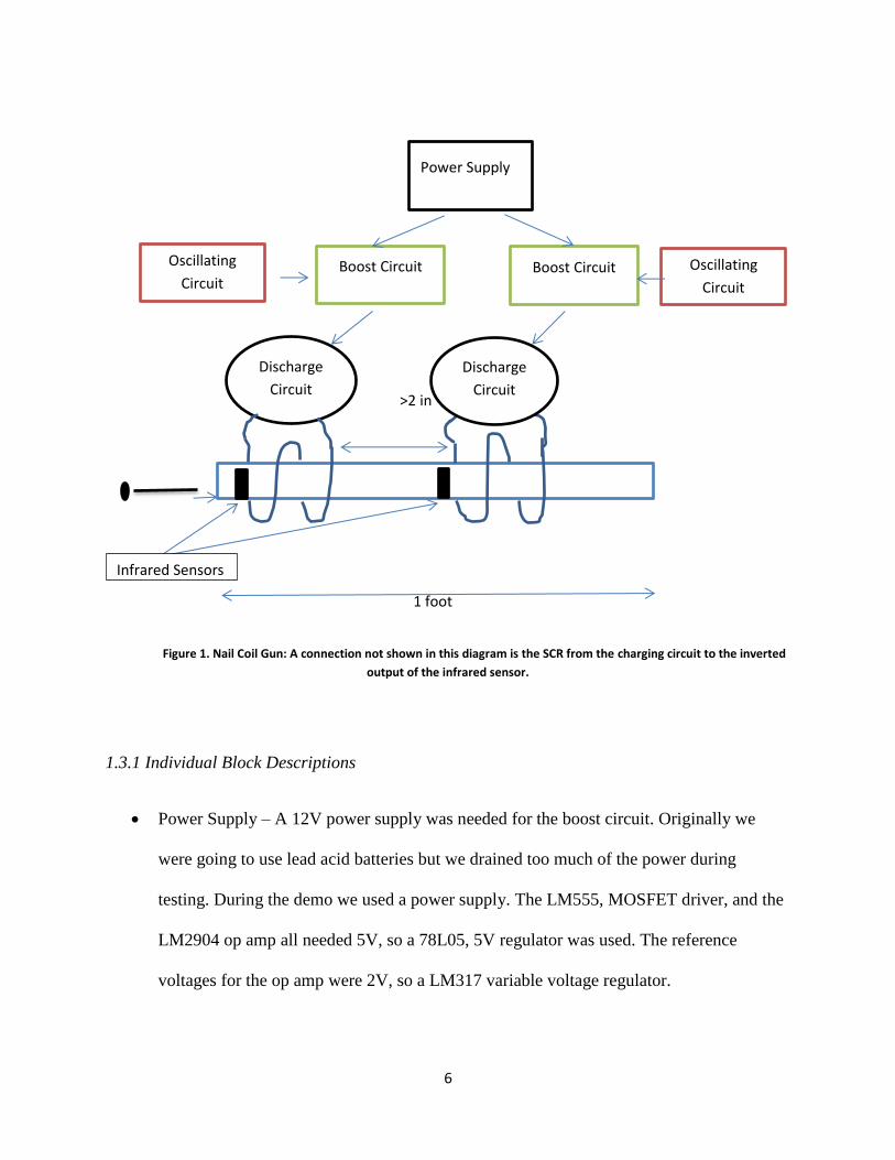
6
1 foot
Figure 1. Nail Coil Gun: A connection not shown in this diagram is the SCR from the charging circuit to the inverted
output of the infrared sensor.
1.3.1 Individual Block Descriptions
Power Supply – A 12V power supply was needed for the boost circuit. Originally we
were going to use lead acid batteries but we drained too much of the power during
testing. During the demo we used a power supply. The LM555, MOSFET driver, and the
LM2904 op amp all needed 5V, so a 78L05, 5V regulator was used. The reference
voltages for the op amp were 2V, so a LM317 variable voltage regulator.
Discharge
Circuit
Boost Circuit Boost Circuit
Power Supply
>2 in
Infrared Sensors
Discharge
Circuit
Oscillating
Circuit Oscillating
Circuit
7
Oscillating Circuit – This is the signal that drives the MOSFET. The LM555 produces a
2kHz square wave. The 555 timer does not source enough current to drive the MOSFET
alone so a MOSFET driver is used to amplify the signal. The output of this circuit is a
5V, 2kHz square wave.
Boost Circuit – This circuit is a boost converter with a 12V input and 350V output. The
output capacitor is a 400V, 680uF capacitor so it can store 40J of energy. The inductor
used in this circuit is about 35mH. There is 500kΩ resistor in parallel with the capacitor
so the capacitor can discharge in approximately 13 minutes when it’s not in use. To
prevent the capacitor from charging to above 350V the bleed resistors are also used as
voltage divider for an input into the op amp.
Discharge Circuit – When the sensor sees a nail the gate of the SCR is triggered which
allows the energy from the capacitor to discharge into the coil. Then the nail should
shoot.
o Sensor – The original signal from the sensor goes from high to low when it’s
blocked. The op amp was used to invert this signal to trigger the SCR.
o Coil –. The two coils are the main component of the gun, and are what supplies
the magnetic field to pull/push the nail through the barrel. The inductance of the
coils is 20uH each.
8
2. Design
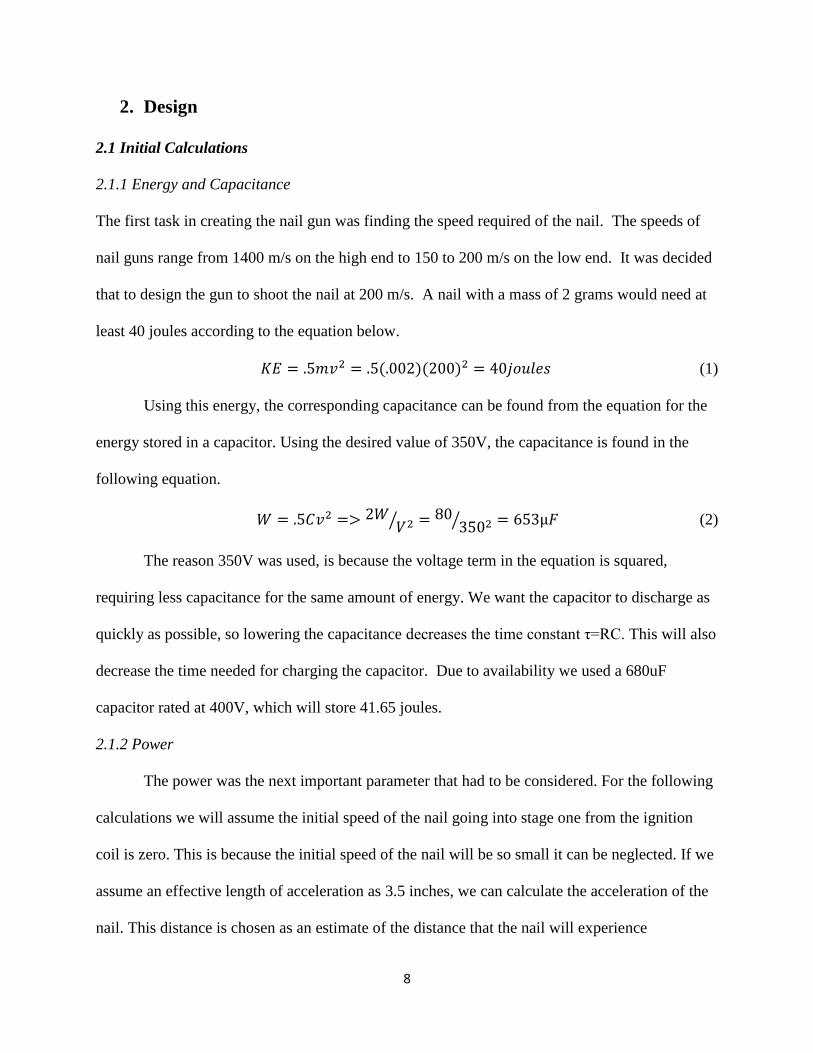
2.1 Initial Calculations
2.1.1 Energy and Capacitance
The first task in creating the nail gun was finding the speed required of the nail. The speeds of
nail guns range from 1400 m/s on the high end to 150 to 200 m/s on the low end. It was decided
that to design the gun to shoot the nail at 200 m/s. A nail with a mass of 2 grams would need at
least 40 joules according to the equation below.
(1)
Using this energy, the corresponding capacitance can be found from the equation for the
energy stored in a capacitor. Using the desired value of 350V, the capacitance is found in the
following equation.
⁄
⁄ (2)
The reason 350V was used, is because the voltage term in the equation is squared,
requiring less capacitance for the same amount of energy. We want the capacitor to discharge as
quickly as possible, so lowering the capacitance decreases the time constant τ=RC. This will also
decrease the time needed for charging the capacitor. Due to availability we used a 680uF
capacitor rated at 400V, which will store 41.65 joules.
2.1.2 Power
The power was the next important parameter that had to be considered. For the following
calculations we will assume the initial speed of the nail going into stage one from the ignition
coil is zero. This is because the initial speed of the nail will be so small it can be neglected. If we
assume an effective length of acceleration as 3.5 inches, we can calculate the acceleration of the
nail. This distance is chosen as an estimate of the distance that the nail will experience
9
acceleration. If we estimate the length that the nail experiences a force as 3.5 inches for each
stage, then we get a distance of 7 inches or 17.78cm. Using the using the following kinematic
equations we get our values:
(3)
Using this acceleration, estimating to 112,500 m/s^2 for ease of calculations we find the
following:
(4)
Therefore, our capacitors must discharge in half of the 1.778ms calculated above. This is
equal to about 5 time constants of the RLC circuit. Since we assumed 50% efficiency the total
discharge time is 3.556ms. Therefore using the equation for the time constant above, it can be
seen that the equivalent resistance seen by the capacitor discharging into the coil will be about
.5Ω. The resistance chosen for the output will be 1 ohm instead, which will help account for the
inherent losses in the components and also keep the current from spiking to high. The power can
now be found using the following equation:
(5)
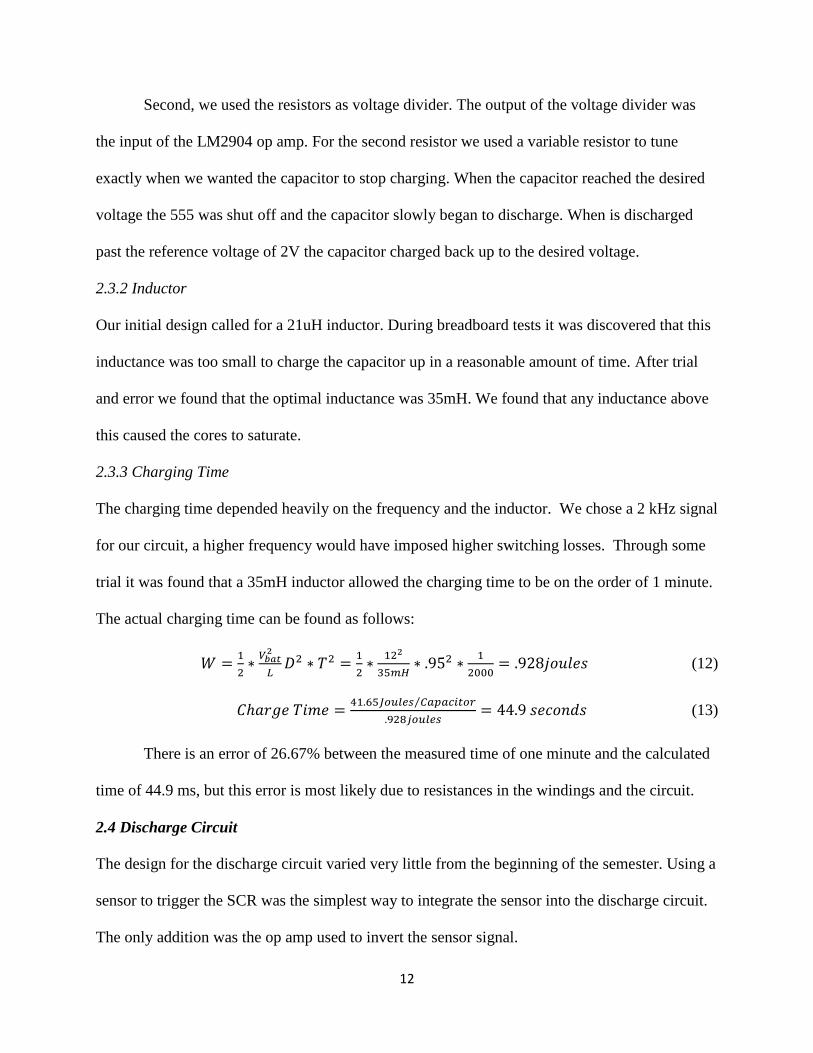
2.2 Oscillating Circuit
We started designing the oscillating circuit by simulating different square waves with the boost
circuit which is discussed in section 2.3. Amplitudes larger than 5V did not improve switching.
The duty cycle was large was to allow the capacitor to absorb the maximum amount of energy in
each cycle. However, at higher duty cycles the MOSFET did not behave properly. Therefore, at
least a 5V peak to peak wave form at a 95% seemed to allow the best switching for the
MOSFET. Switching a MOSFET at high frequencies could damage the part, so we kept the
frequency at 2kHz and made up for it with the largest possible duty cycle [6].
10
To create this square wave we considered different oscillators such as the AD2S99
programmable oscillator, but these parts were not readily available. The LM555 timer was a
familiar analog wave form generator that could be found in the ECE Electronics Service Shop.
The amplitude, duty cycle, and frequency were easily controlled with the LM555. If we needed
to the any of those factors it was done easily.
The design was based off of the NE555 [2] design specifications for astable operation.
The calculations are done below.
(6)
This value was chosen so that .
(7)
(8)
(9)
One kilo-ohm was chosen so that the frequency could lie anywhere between 10Hz –
100kHz. To get to the frequency to 2kHz the capacitance for C2 = .67uF. The output of this
circuit is than amplified by the MOSFET driver. Figure 3 in section 2.6 shows the oscillating
circuit.
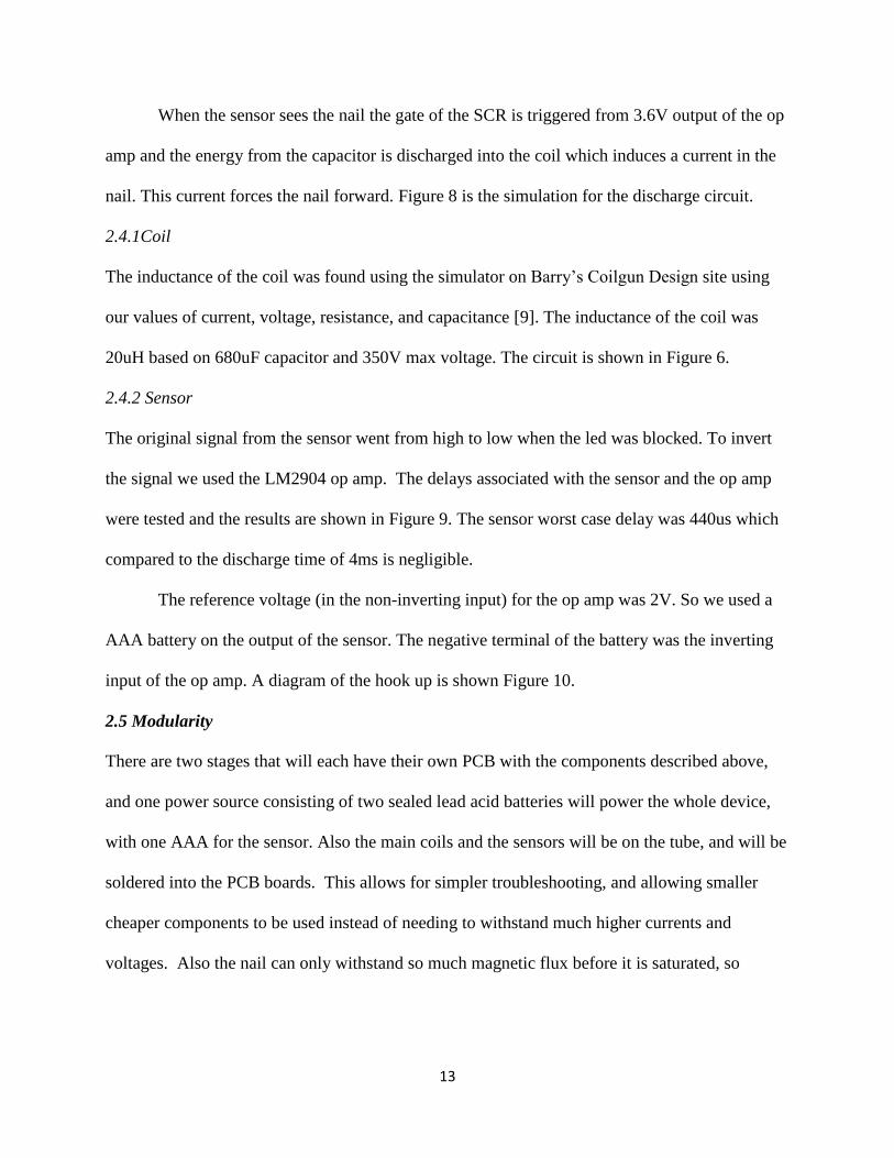
For the actual circuit 909Ω and 56Ω are used instead 900Ω and 50Ω respectively. Figure
4 is the output of the oscillating circuit. The top (yellow) wave form is the 555 output. The
bottom (green) wave form is the MOSFET driver output.
11
Figure 4 above shows that the output of the MOSFET driver is 8.3V. On the actual PCB
with larger components drawing more current, the MOSFET driver output was actually 5.3V
which was the needed peak to peak voltage to drive the boost circuit.
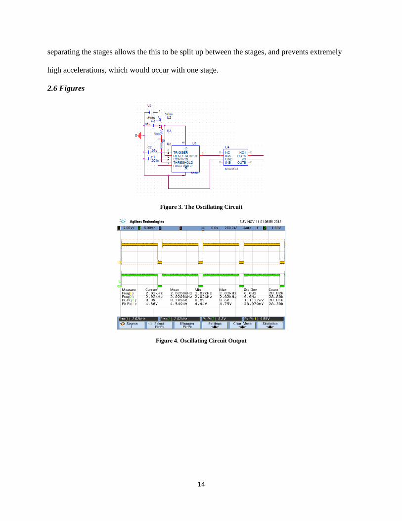
2.3 Boost Circuit
For the boost circuit we needed to charge a fairly large capacitor to high voltage in a reasonable
amount (less than 2 minutes). We started with a transformer design. To get the voltage on the
capacitor up to 350V we needed an input voltage of 20V and a transformer ratio of 10uH to
10000uH. Transformers of this size were physically large and expensive and winding our own
transformer would have been tedious and time consuming. Even though the charging time with
the transformer was faster, a boost converter in CCM mode was chosen. This way the capacitor
could charge up to 350V at lower input voltage (12V-15V) [11].
In the boost circuit the capacitor is charged to 350V. A 600V rectifier diode, 600V Vds
NPN MOSFET, and a 400V capacitor are used in the actual circuit. The oscillating circuit output
is connected to the gate of the MOSFET and this drives the boost circuit. When the MOSFET is
an open the charge stored in the inductor is dumped into the capacitor. A simulation of the
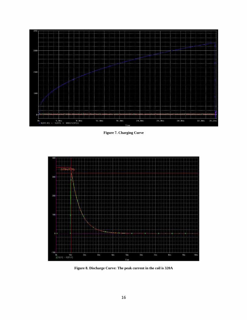
charging curve is in Figure 7.
2.3.1 Bleed Resistors
The resistors in parallel with the capacitor serve two purposes. The first is they are bleed
resistors. With 500kΩ resistor the capacitor would discharge to 35V in 13 minutes when it’s not
in use. Also, since 500kΩ is a high resistance, the capacitor wouldn’t charge too slowly.
⁄
⁄
(10)
(11)
12
Second, we used the resistors as voltage divider. The output of the voltage divider was
the input of the LM2904 op amp. For the second resistor we used a variable resistor to tune
exactly when we wanted the capacitor to stop charging. When the capacitor reached the desired
voltage the 555 was shut off and the capacitor slowly began to discharge. When is discharged
past the reference voltage of 2V the capacitor charged back up to the desired voltage.
2.3.2 Inductor
Our initial design called for a 21uH inductor. During breadboard tests it was discovered that this
inductance was too small to charge the capacitor up in a reasonable amount of time. After trial
and error we found that the optimal inductance was 35mH. We found that any inductance above
this caused the cores to saturate.
2.3.3 Charging Time
The charging time depended heavily on the frequency and the inductor. We chose a 2 kHz signal
for our circuit, a higher frequency would have imposed higher switching losses. Through some
trial it was found that a 35mH inductor allowed the charging time to be on the order of 1 minute.
The actual charging time can be found as follows:
(12)
⁄
(13)
There is an error of 26.67% between the measured time of one minute and the calculated
time of 44.9 ms, but this error is most likely due to resistances in the windings and the circuit.
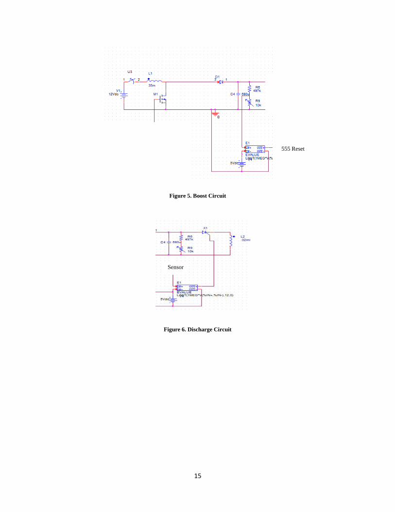
2.4 Discharge Circuit
The design for the discharge circuit varied very little from the beginning of the semester. Using a
sensor to trigger the SCR was the simplest way to integrate the sensor into the discharge circuit.
The only addition was the op amp used to invert the sensor signal.
13
When the sensor sees the nail the gate of the SCR is triggered from 3.6V output of the op
amp and the energy from the capacitor is discharged into the coil which induces a current in the
nail. This current forces the nail forward. Figure 8 is the simulation for the discharge circuit.
2.4.1Coil
The inductance of the coil was found using the simulator on Barry’s Coilgun Design site using
our values of current, voltage, resistance, and capacitance [9]. The inductance of the coil was
20uH based on 680uF capacitor and 350V max voltage. The circuit is shown in Figure 6.
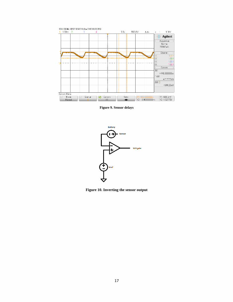
2.4.2 Sensor
The original signal from the sensor went from high to low when the led was blocked. To invert
the signal we used the LM2904 op amp. The delays associated with the sensor and the op amp
were tested and the results are shown in Figure 9. The sensor worst case delay was 440us which
compared to the discharge time of 4ms is negligible.
The reference voltage (in the non-inverting input) for the op amp was 2V. So we used a
AAA battery on the output of the sensor. The negative terminal of the battery was the inverting
input of the op amp. A diagram of the hook up is shown Figure 10.
2.5 Modularity
There are two stages that will each have their own PCB with the components described above,
and one power source consisting of two sealed lead acid batteries will power the whole device,
with one AAA for the sensor. Also the main coils and the sensors will be on the tube, and will be
soldered into the PCB boards. This allows for simpler troubleshooting, and allowing smaller
cheaper components to be used instead of needing to withstand much higher currents and
voltages. Also the nail can only withstand so much magnetic flux before it is saturated, so
14
separating the stages allows the this to be split up between the stages, and prevents extremely
high accelerations, which would occur with one stage.
2.6 Figures
Figure 3. The Oscillating Circuit
Figure 4. Oscillating Circuit Output
15
Figure 5. Boost Circuit
Figure 6. Discharge Circuit
555 Reset
Sensor
16
Figure 7. Charging Curve
Figure 8. Discharge Curve: The peak current in the coil is 320A
17
Figure 9. Sensor delays
Figure 10. Inverting the sensor output
18
3. Verification
Our requirement and verification table details the process for complete testing of the circuit, and
is located in Appendix A.
3.1 Power Supply
To test the power supply, we probed the voltage output of the 5V regulator and the 2V regulator
and made sure these voltages were seen by the logic circuits. Also 12V had to be supplied to the
boost circuit.
3.2 Oscillating Circuit
The 555 timer had to output a 2 kHz square wave at 5V peak to peak. This signal then had to be
amplified to 5 to 8V by the MOSFET driver. A probe on pin seven of the MOSFET driver will
show full functionality of oscillating circuit.
3.3 Boost Circuit
To test the boost circuit we used two 12V lead acid batteries in parallel to source enough current.
This way the capacitor charged faster. We probed the cathode of the diode to ground with a high
impedance probe for the oscilloscope. We did each stage separately at first then we connected
the two stages together.
When the batteries discharged we had to use the power supply, which sourced too much
current and damaged the MOSFETs. So when using the power supply we started the input
voltage at 6V and slowly raised the voltage to 12V so that the current never exceeded 100mA.
With a 35mH inductor we were able to charge the capacitors to within 10% 350V in about 1
minute.
3.4 Discharge Circuit
19
To test the discharge circuit we put a small resistance on the output of the capacitor. Then we
blocked the sensor with the nail and using the voltmeters we saw the capacitor discharge
immediately.
3.5 Failed Verification
Verification 7 failed and so the gun did not shoot. We do not know the exact cause. Possible
causes are discussed in section 5.2.2. To complete this verification, we have made new PCBs.
We are currently testing these boards.
20
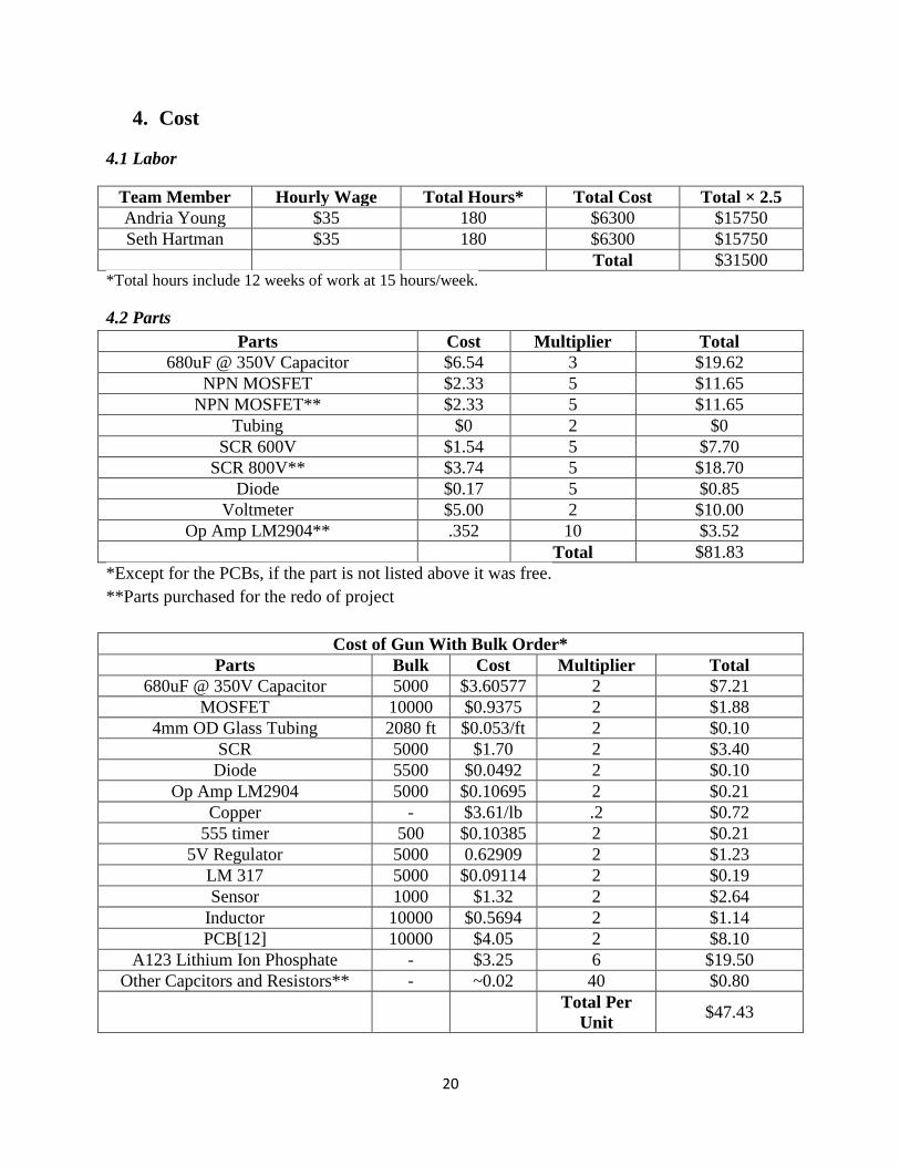
4. Cost
4.1 Labor
Team Member Hourly Wage Total Hours* Total Cost Total × 2.5
Andria Young $35 180 $6300 $15750
Seth Hartman $35 180 $6300 $15750
Total $31500 *Total hours include 12 weeks of work at 15 hours/week.
4.2 Parts
Parts Cost Multiplier Total
680uF @ 350V Capacitor $6.54 3 $19.62
NPN MOSFET $2.33 5 $11.65
NPN MOSFET** $2.33 5 $11.65
Tubing $0 2 $0
SCR 600V $1.54 5 $7.70
SCR 800V** $3.74 5 $18.70
Diode $0.17 5 $0.85
Voltmeter $5.00 2 $10.00
Op Amp LM2904** .352 10 $3.52
Total $81.83
*Except for the PCBs, if the part is not listed above it was free.
**Parts purchased for the redo of project
Cost of Gun With Bulk Order*
Parts Bulk Cost Multiplier Total
680uF @ 350V Capacitor 5000 $3.60577 2 $7.21
MOSFET 10000 $0.9375 2 $1.88
4mm OD Glass Tubing 2080 ft $0.053/ft 2 $0.10
SCR 5000 $1.70 2 $3.40
Diode 5500 $0.0492 2 $0.10
Op Amp LM2904 5000 $0.10695 2 $0.21
Copper - $3.61/lb .2 $0.72
555 timer 500 $0.10385 2 $0.21
5V Regulator 5000 0.62909 2 $1.23
LM 317 5000 $0.09114 2 $0.19
Sensor 1000 $1.32 2 $2.64
Inductor 10000 $0.5694 2 $1.14
PCB[12] 10000 $4.05 2 $8.10
A123 Lithium Ion Phosphate - $3.25 6 $19.50
Other Capcitors and Resistors** - ~0.02 40 $0.80
Total Per
Unit $47.43

21
*Doesn’t include housing of gun
**Assuming Conservatively Max Cost is 2 cents per unit
4.3 Total Cost
Parts + Labor = $49.82 + $31,500 = $31,549.82 (14)
22
5. Conclusion
5.1 Accomplishments
The circuit was fully functional, except for test firing the nail, the night before the demo.
The setup for firing the nail matched our expectations, because we found a tube very close to the
diameter of the nail, while still allowing the sensors to sense the nail. We were able to get the
boost circuit to charge the capacitors to 350V as specified. This meant full functionality of the
555 timer circuit and MOSFET driver, supplying the 2 kHz signal to the gate of the MOSFET.
Although we had troubles later on with the PCB, we were able to charge the capacitor to 350V
using just the sealed lead acid batteries. The comparator recognized the 350V and prevented
further charging as per design. Also we were also able to discharge the capacitor after by
tripping the sensor and using a resistor as the output load. We are currently in the process of
rebuilding the circuits, and have ordered new PCB’s and parts. Our hopes are to achieve full
functionality before the end of the semester.
5.2 Uncertainties
5.2.1 MOSFET
A problem we encountered when testing was that we found that we were blowing out the
MOSFETs. When beginning to charge the capacitor, there is a current spike because the inductor
starts out as a short. We believe this the reason our MOSFETs stopped working. To solve this we
start charging at 6V and raise the voltage slowly so that the current wouldn’t go above 100mA.
We never tested out limiting this current spike and using a constant 12V source.
5.2.2 Discharge Circuit
Another problem we encountered was that our discharge circuit stopped working. We believe it
was because during the demo we hooked up the AAA battery incorrectly. We removed the
23
sensors and tested them with the op amp on the breadboard and the sensor wasn’t damaged, but it
no longer worked on the PCB. All other functions of the circuit were working and MOSFET and
SCR were behaving properly. We tested each stage separately with the same results. Because we
couldn’t solve problem we decided to get all new PCBs and parts.
The desired discharge time was less than half of the actual discharge time. To
compensate for this we moved the coils closer together to about 2 inches. Having not been able
to shoot the gun we are unsure if this change in design will allow for the gun to shoot past the
first stage.
5.2.3 Sensor Hook Up
When using the AAA battery for the sensor output we thought since the voltage of the battery is
1.5V that the reference voltage would be equal to that. However the sensor/op amp hook up did
not work until the reference voltage was set to 2V. We don’t know why this is, but the only thing
we needed to change because of this was the voltage divider output for the bleed resistors. We
adjusted with the variable resistor.
5.3 Future Work / Alternatives
While working on the project several mistakes in the initial design, or more advanced ideas came
up as future design options. The capacitors take over a minute to charge, so speeding up the
charge time would be important for the design to be made more practical for regular use. In
order to do this, the frequency could be increased, which would also make the circuit small
because the inductor size would decrease. The boost circuit would be run on the edge of the
discontinuous conduction mode so that all of the energy stored in the inductor is transferred to
the capacitor in one cycle. A bank of capacitors could also be added so that after one capacitor
discharged it would immediately start recharging, and the next capacitor could be used to fire the

24
next nail. This would increase the size of the circuit slightly but would allow for rapid
succession firing of the nails.
Another improvement would be to create a portable housing that is nonconductive and
able to withstand appropriate forces of the gun, and the coils, and also able to supply a
continuous stream of nails to the firing tube. In order to make it portable lithium ion phosphate
batteries would be the best option for they provide a large energy density, and would lighten the
load. An A123 Lithium Ion Phosphate Batteries supplies the following amount of energy using
the energy density of 108.10 Watt-Hours per kilogram [10]:
(
) (15)
(16)
This assumes no losses, but does present a significant number of nails that can be fired on
a single charge of the rechargeable battery back, and switching out battery packs would allow for
immediate continued use. Solar panels could be added for longer use, which would be beneficial
since nail guns are often used outside, on roofs for example.
5.4 Ethical Considerations
Our project may encounter ethical issues since we are dealing with very high voltages. We will
disclose any new findings in data and calculations they may change the course of our project. We
will also make sure to be truthful in our labeling of high voltage components. This follows this
ethic from 7.8 of the IEEE code of ethics:
“1.) To accept responsibility in making decisions consistent with the safety, health, and welfare
of the public, and to disclose promptly factors that might endanger the public or the
environment”

25
We will also, and have already taken into account the possibility of injuries involved, and
have equipped the gun with appropriate safety measures. The voltage is prevented from going
above the specified 350V limit using the comparator. Also we had a Plexiglas shield put in front
of the gun, and the demo will be done behind another shield, in order to protect observers from
projectiles. Full implementation of the design for customer use would undergo rigorous testing
and extra safety precautions. This follows the ethic from 7.8 of the IEEE code of ethics:
9.) “to avoid injuring others, their property, reputation, or employment by false or malicious
action”
26
6. References
[1] LM2904, datasheet, Texas Instruments, 2010. Available at:
http://www.ti.com/lit/ds/symlink/lm358.pdf
[2] LM555/NE555/SA555: Single Timer, datasheet, Fairchlid Semiconductor. Available at:
http://www.utsource.net/pdf/pdf-LM555CN.html
[3] All About Batteries, webpage, Available at: http://www.allaboutbatteries.com/Energy-
tables.html. Accessed September 2012.
[4] How Nail Guns Work, webpage, Available at: http://home.howstuffworks.com/nail-
gun4.htm. Accessed September 2012.
[5] 2N6504: Silicon Controlled Rectifiers, datasheet, ON Semiconductor, 2008. Available at:
http://www.onsemi.com/pub_link/Collateral/2N6504-D.PDF
[6] AOT15S60/AOB15S60/AOTF15S60 600V 15A a MOS Power Transistor, datasheet,
Alpha and Omega Semiconductor, 2011. Available at:
http://aosmd.com/res/data_sheets/AOB15S60.pdf
[7] LM317 3-Terminal Positive Adjustable Regulator, datasheet, Fairchild Semiconductor,
2011. Available at: http://www.fairchildsemi.com/ds/LM/LM317.pdf
[8] LM78LXX Series 3-Terminal Positive Regulators, datasheet, National Semiconductor,
2000. Available at: http://www.futurlec.com/Linear/78L05.shtml
[9] Barry’s Coilgun Designs, webpage, Available at:
http://www.coilgun.info/about/home.htm. Accessed September 2012.
[10] Powerizer, webpage, Available at: http://www.batteryspace.com/a123-system-
nanophosphate-lifepo4-26650-rechargeable-cell-3.2v-2500-mah.aspx. Accessed December
2012.
[11] Power Supply Design, webpage, Available at:
http://www.smpstech.com/mtblog/continuous_ccm_and_discontinuous_conduction_mode_d
cm.html. Accessed December 2012.
[12] PCB Design, webpage, Available at: http://www.ladyada.net/library/pcb/costcalc.html.
Accessed December 2012.
27
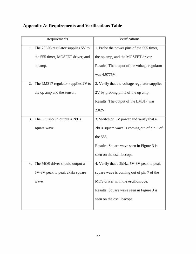
Appendix A: Requirements and Verifications Table
Requirements Verifications
1. The 78L05 regulator supplies 5V to
the 555 timer, MOSFET driver, and
op amp.
1. Probe the power pins of the 555 timer,
the op amp, and the MOSFET driver.
Results: The output of the voltage regulator
was 4.9775V.
2. The LM317 regulator supplies 2V to
the op amp and the sensor.
2. Verify that the voltage regulator supplies
2V by probing pin 5 of the op amp.
Results: The output of the LM317 was
2.02V.
3. The 555 should output a 2kHz
square wave.
3. Switch on 5V power and verify that a
2kHz square wave is coming out of pin 3 of
the 555.
Results: Square wave seen in Figure 3 is
seen on the oscilloscope.
4. The MOS driver should output a
5V-8V peak to peak 2kHz square
wave.
4. Verify that a 2kHz, 5V-8V peak to peak
square wave is coming out of pin 7 of the
MOS driver with the oscilloscope.
Results: Square wave seen in Figure 3 is
seen on the oscilloscope.
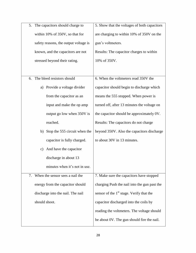
28
5. The capacitors should charge to
within 10% of 350V, so that for
safety reasons, the output voltage is
known, and the capacitors are not
stressed beyond their rating.
5. Show that the voltages of both capacitors
are charging to within 10% of 350V on the
gun’s voltmeters.
Results: The capacitor charges to within
10% of 350V.
6. The bleed resistors should
a) Provide a voltage divider
from the capacitor as an
input and make the op amp
output go low when 350V is
reached.
b) Stop the 555 circuit when the
capacitor is fully charged.
c) And have the capacitor
discharge in about 13
minutes when it’s not in use.
6. When the voltmeters read 350V the
capacitor should begin to discharge which
means the 555 stopped. When power is
turned off, after 13 minutes the voltage on
the capacitor should be approximately 0V.
Results: The capacitors do not charge
beyond 350V. Also the capacitors discharge
to about 30V in 13 minutes.
7. When the sensor sees a nail the
energy from the capacitor should
discharge into the nail. The nail
should shoot.
7. Make sure the capacitors have stopped
charging Push the nail into the gun past the
sensor of the 1st stage. Verify that the
capacitor discharged into the coils by
reading the voltmeters. The voltage should
be about 0V. The gun should fire the nail.

29
Results: The capacitor energy does not
discharge in the coil. The gun did not shoot.
30
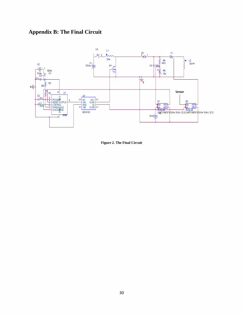
Appendix B: The Final Circuit
Figure 2. The Final Circuit