Embed Size (px)
Citation preview
3rd NASA Symposium on VLSI Design 1991
N94-183493.5.1
An Improved Distributed Arithmetic Architecture
X. Guo and D. W. Lynn
NASA Space Engineering Research Center for VLSI System Design
University of Idaho
Moscow, Idaho 83843
AbJtract- Speed requirements have been, and will continue to be a major con-
sideration in the design of hardware to implement digital signal processing
functions like digital filters and transforms llke the DFT and DCT. The con-
ventional approach is to increase speed by adding hardware and increasing
chip area. The real challenge is to save chip area while still maintaining high
speed performance. The approach we propose is based on the distributed
arithmetic implementation (DA) of digital filters. The improvement is based
on two observations. Firstly, a single memory element can replace several
identical memory elements in a fully parallel DA implementation. Secondly_
truncation or rounding may be introduced into the computation at strategic
points without increasing error unduly. Both of these approaches can be used
to attain area savings without impairing speed of operation.
1 Introduction
Finding the inner product between two vectors is an operation that commonly arises in sig-
nal processing as well as in general data processing. Digital convolution and correlation are
directly described as inner products. Other operations such as the discrete Fourier trans-
form and other common transforms can be implemented as a sequence of inner products.
Consider the inner productK
y = (1)k=l
In the case of a FIR digital filter, At, represents a set of fixed weights, and zk represents
the current and past K - 1 filter inputs. The inner product can be implemented directly
by using a single multiplier and an accumulator in a serial one product at a time manner,
as in Figure 1, or in a fully parallel manner by using K multipliers and a multi-input adder
or adder tree, as in Figure 2. Obviously, the fully parallel architecture will always be faster
than the serial approach.
The distributed arithmetic (DA) approach to computing the inner product was devel-
oped in the early seventies [1,2,3,4,5,6,7,8]. In this approach, combinations of the Ak are
precomputed and stored in memory. Input data are used to identify which memory words
are to be fetched, shifted and added to produce the final result. Without loss of generality,
This research was supported in part by NASA under grant NAGW-1406.
https://ntrs.nasa.gov/search.jsp?R=19940013876 2018-06-07T20:19:23+00:00Z

3.5.2
xk
Y
Figure I: Multipller-Accumulator Implementation
0 0 0
A 2
--- yr
i_igure 2: Fully Parallel Direct imp|emen_a_ion
_rs_ assume that the zk are scaJed such that l_kl < 1. In two_scomp]eement iorm
M-I
........ •_ -b_0+ _ b_2-_ (2)wt-----1
where the bk,,, represent the individual bits in zk with bk0 the sign bit. Substituting (2)
into (1) and rearranging the order of summation gives
y = _ A_b_ 2-_ - Z A_b_0 (31m=l k=l
Since the bits bi,,_ are either 0 or 1 the term K, El,=1 A_,bk,._ can be precomputed for all
2 K possible combinations of b_,,,. These vaJues are then stored in a ROM or RAM. The
actual combina_ns of bk,_, a_s_g outof the input clara, are used to address one of the
precomputed terms stored in the memory. Note that these combinations are formed by
selecting the ruth bit from each of the K M-bit input words. The mth term so addressed
is then shifted by m bits to the right before being added to the other M terms. The only
exception to this is when m = 0. In this case, which corresponds to using the sign bits of
the input data to form the address, the addressed term is subtracted from the other terms.
As with the direct implementation of the inner product, there are two approaches to
implementing DA. The inner product can be computed by using only one memory and a
single accumulator as shown in Figure 3, or in a fully parallel manner by using M memories,
=
=
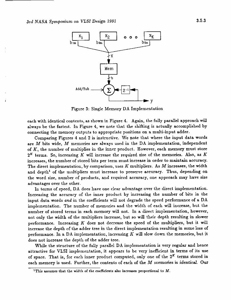
3rd NASA Symposium on VLSI Design 1991 3.5.3
I I I I IxKXl x2 o o o
IMeml
Add/Sub @_
..-y
Figure 3: Single Memory DA Implementation
each with identical contents, as shown in Figure 4. Again, the fully parallel approach will
always be the fastest. In Figure 4, we note that the shifting is actually accomplished by
connecting the memory outputs to appropriate positions on a multi-input adder.
Comparing Figures 4 and 2 is instructive. We note that where the input data words
are M bits wide, M memories are always used in the DA implementation, independent
of K, the number of multiplies in the inner product. However, each memory must store
2 K terms. So, increasing K will increase the required size of the memories. Also, as K
increases, the number of stored bits per term must increase in order to maintain accuracy.
The direct implementation, by comparison, uses K multipliers. As M increases, the width
and depth 1 of the multipliers must increase to preserve accuracy. Thus, depending on
the word size, number of products, and required accuracy, one approach may have size
advantages over the other.
In terms of speed, DA does have one clear advantage over the direct implementation.
Increasing the accuracy of the inner product by increasing the number of bits in the
input data words and in the coefficients will not degrade the speed performance of a DA
implementation. The number of memories and the width of each will increase, but the
number of stored terms in each memory will not. In a direct implementation, however,
not only the width of the multipliers increase, but so will their depth resulting in slower
performance. Increasing K does not decrease the speed of the multipliers, but it will
increase the depth of the adder tree in the direct implementation resulting in some loss of
performance. In a DA implementation, increasing K will slow down the memories, but it
does not increase the depth of the adder tree.
While the structure of the fully parallel DA implementation is very regular and hence
attractive for VLSI implementation, it appears to be very inefficient in terms of its use
of space. That is, for each inner product computed, only one of the 2 K terms stored in
each memory is used. Further, the contents of each of the M memories is identical. Our
tThis assumes that the width of the coefficients also increases proportional to M.
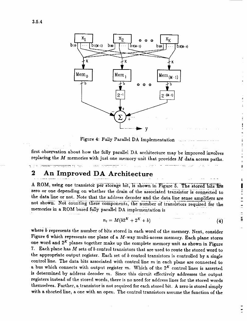
3.5.4
Xl x2 o o o XK
Mem 0 1
oo
Figure 4: Fully ParallelDA Implementation ..............
firstobservation about how the fully parallelDA architecture may be improved involves
replacing the M memories with just one memory unit that provides M data access paths.
2 An improved DA Architecture
A ROM, using one transistorper storage blt,is shown in Figure 5. The store_F_|_s_
zero or one depending on whether the drain of the associated transistori_onnected to
the data lineor not. Note that the address decoder and the data llnesense amplifiersare
not shown. Not counting these components_ the:numbcr Of transistorsrequired for ths
memories in a ROM based fullyparallelDA implementation is
rtt = M(b2 K + 2 _ + b) -- (4)
where_represents the number of bits stored in each word of the memory. Next, consider
Figure 6 which represents one plane of a M-way multi-access memory. Each plane stores
one word and 2K planes together make up the complete memory unit as shown in Figure
7. Each plane has M sets of b control transistors that are used to route the stored word to
the appropriate output register. Each set of b control transistors is controlled by a single
control line. The data bits associated with control line m in each plane are connected to
a bus which connects with output register m. Which of the 2 K control lines is asserted
is determined by address decoder m. Since this circuit effectively addresses the output
registers instead of the stored words, there is no need for address lines for the stored words
themselves. Further, a transistor is not required for each stored bit. A zero is stored simply
with a shorted llne, a one with an open. The control transistors assume the function of the

3rd NASA Symposium on VLSI Design 1991 3.5.5
address line ! VDD___ VDD 1
I I
_2_
precharg_e t
address line
precharg_eI
address line 2K__I_
precharg_eI_ "-"._
stored 1
i
@
o
VDD
precharge
Figure 5: ROM Architecture
storage transistors in the ROM architecture, and provide a path between every stored word
in the memory unit and every output register. The total number of transistors required to
implement the memory unit, again excluding address decoders and output registers is
nt : Mb2 g + b2 K -4- 2 g (5)
Note that both approaches use M K to 2 K decoders and identically sized adder trees. The
ratio of the number of transistors in the storage sections of the Multi-Access memory unit
and the memories in a fully parallel DA architecture give an estimate of the area savings
potential presented by one approach over the other. Dividing (5) by (4) gives
Mb2 K + b2 g + 2 K Mb2 K + (b + 1)2 K
Ra,e_ = Mb2K + M2 K + Mb = Mb(2 _ + 1) + M2 K (6)
Since b will usually be greater than M, Ra_e_ > 1. That is, the multi-access memory
architecture presents no area savings, despite the fact it replaces M copies of each stored

3.5.6
j°° ,j°° VDD
control line I l_
control line 2
data bit 1
data bit b
data bit 1
data bit b
stored 0 tored 1
data bit i
data bit b
bus I
bus 2
bus M
Figure 6: Memory Unit Plane
word with just one copy. This is because the expense of bus controls erases the savings of
memory transistors. In fact the number of transistors associated with stored bits in the
fully parallel implementation is Mb2 K. This is also the number 0f bus control trans_st0rs
in the muir-l-access memory. However, for memory architectures where there is more than
one transistor per stored bit, the savings in storage transistors will not be absorbed by bus
control transistors. To see this, consider the case that 4 transistor static RAM cells are
used as memory elements. Static RAM may be required in cases where the inner product
is to be configurable, in the sense that the coemcients may be changed from time to time,_
requiring tl_e memory contents to be rewritten. The conventional static _ architecture
_=i_sshown in Figure 8 and one pl_ane or the m_ti_access memory architecture is shown in
Figure 9.
A fully parallel implementation of DA using M static RAMs of the type shown in
" Fi---gure-8-would use 4Mb2 K t_an_is{0rs and ._b2g ce_ seiect transistors-. The static-R._M
multi-access memory unit would use 4b2 K transistors for storage and Mb2 K bus control
transistors. Thus, when static RAM cells are used,
R_,_ - (M + 4)b2 K M + 45Mb2 K - 5M (7)
Here there will be an area savings so long as M (the number of bits in the input data words
and the number of memory units in the fully parallel DA implementation) is greater then 1.

3rd NASA Symposium on VLSI Design 1991
decoder 2 /
plane 3 K
plane 8 ]
plane 1
J
bus I
I bus M
3.5.7
Figure 7: Multi-Access Memory Unit
If M = 8, R_,_o = .30. Thus the area savings can be significant. These observations have
been made in the context that the number of transistors corresponds to area requirements.
The same results hold whenever the area required for the storage cell (be it transistor based
or not) requires more area to implement than do bus control transistors• Again, it must be
noted that whiIe the area required for address decoders and the adder tree are the same for
both implementations, these requirements are not included in the Ra,ea computation. So,
Ra,_, only reflects the savings potential in the storage section of the implementation. To
the degree that the storage section dominates the other elements of the implementation this
may translate into significant savings. Not only do the other dements need to be included
in the computations, but an actual VLSI layout of a multi-access memory based DA circuit
needs to be attempted to make sure that the connection complexity of the multi-access
memory unit does not overwhelm what appears to be a significant area savings potential
in the case of static RAM memory cells.
3 Truncation and Rounding
Once each term is fetched from the memory, they are shifted and added to form the final
result. This operation is diagramed in Figure 10. If each memory in a fully parallel imple-
mentation stores terms that are b bits wide, then the resulting inner product will occupy
3.5.8
address line1
....vbv: _L
addressline2K
=L. -...L
_L_
b:
_L_
Figure 8: StaticRAM
at most M + b bitsJ Suppose, however, that the product only needs to be determined to
an accuracy of f significantbits.In thiscase itmay be possible to truncate or round the
individual terms before adding. Doing so would not only reduce the amount of har_c[ware
req_ired_n:i_e adder-tree,13u_o_ _o r-edti_ _s_ze_ofsome 0f the mem_ries__his
-_S o_l_vi-ous in-the c-ase oft-_- he_fufly parcel DA i-_mple-rnentafion and-, as _e_l_ see i_/_er,- i_
-iS-also true-for-the _muRi-access merfiory Unit based-imt_lement-M]on.°F_r°st_ie_t- "us consider
what the impact of truncating or rounding wifl be on the accuracy of the final resffft.
Truncating the individual terms and discar_ding bits that fall in column ] + e and to
the right (as shown in Figure 10) will give a maximum worst case error of
Eu = 2-'((M + b- (/+ e)) - 1 + 2 -(M+b-(/+'))) (8)
where we have normalized the result so that the binary point falls just to the left of column
/.3 The worst case truncation error is calculated by considering that all the truncated bits
-are o_es.
When we round the individual terms and then discard bits that fall in column / + e
there are two worst case error situations. If the bits in column / -{- e are all ones, and all
bits to the right are zeros. In this case the error is
E,° : 2-('+_)(M + b- (/+ e)) (9)
2This can be shown by temporarily treatingthe terms as whole integersand assuming that allM terms
take on the maximum value (2_ - 1). The finalsum willthen be (2_ - 1)* (2M - 1) which can be written
as ((2_+M - 1) - (2M - 1)- 2_)+ I. When written thisway and assuming M < b itiseasy to see that the
resultoccupies at most M + b bits.
aWe also need f __b.
E

3rd NASA Symposium on VLSl Design 1991 3.5.9
control line I i_
r .......... '
, gDD gDD ,
---_ceU 2Zi
gem
c011b:
data bit
data bit 1
data bit b
bus 1
bus M
Figure 9: StaticRAM Multi-Access Memory Plane
Ifthe bits in column f + e are zeros and allthe bitsto the right are ones, the error is
E, tb -- 2-(_+1)((M + b - (f + e + 1)) - 1 + 2 -{M+_-(f+'+1))) (lO)
After the individual terms have been truncated or rounded to f -b e bits, the final sum
is computed and then either truncated or rounded to f bits. This second truncation or
rounding will add to the total error. In the case of truncation, the worst case error will be
Et/= 1 - 2 -(_-I) (11)
In the case of rounding, the additional worst case errors are
E,J. =2-1 (12)E, fb = 2 -I - 2 -(_-I)
Noting that E,.t,, > E, tb and E,.t,, > Ertb, we will use E_to and E_Io when referring to
rounding. There are four possible approaches to arriving at the final result depending on
which of truncation or rounding is applied to the individual terms and which is applied
to the final sum. The four possibilities are summarized in Figure 11. From the graph, we
see that as few as five or six extra bits beyond f are required in order to arrive at errors
that are very near what we would expect if we retained all the bits in the individual terms,

3.5.10
FI
]
b bit terms
1 final sum
II
I0
retain f bits
M terms
If+e M+b-1
discard t bits
Figure 10: The Final Sum
formed the sum and rounded or truncated the result to f bits. We also note {hat tl_s is true
independent of Whether the individual terms are first truncated or rounded. When e .< 4,
the error resulting from rounding is similar to the error resulting from truncating one less
bit. These 0bservations_ suggest that there is not a great deal to be gained by rounding
individual terms over truncating them. In the case of a fully parallel DA implementation,
the rounding of individual terms can be precomputed and only the rounded terms stored,
so there is no cost in doing so. However in the multi-access memory based implementation,
rounding of individual terms would have to be performed upon access. As We shall s-ee
shortly_ the area requirement of the multi-access memory for rounding will be the same
for a memory the truncates one less bit. This, coupled with the above observatigns on
error, indicate that rounding individual terms does not provide a very great advantage
over truncation in the muiti:accessmemory. ........
4 Implementing Truncation and Rounding
First we consider the transistor cost of a ROM based fully parallel DA implementati6n.
From Figure 10 we see that if we desire to compute the final sum to f + e bits, we will need
(M - t) ROMs storing b bit words, and t ROMs that each store one bit less in succession
wheret = (M + b) - (] + e). Note that forc0ns{siency, t < b andt _ M. Ift _> b, M
should be reduced and if t > M, b should be reduced. Now, referring to Figure 5 we see
that for each bit truncated, 2g + i transistors are Saved. Since = + 1)/2, thecost of the implemcntation is
n, = M(b_. _ + 2 x + b) t(t + 1)(2K + 1) (13)2
|

3rd NASA Symposium on VLSI Design 1991 3.5.11
k-
0k-
I..
I,I
"U
N.B
Ek-
OZ
8
7
6
5
4
3
2
1
00
M=16, b=32, f=32
I I I I I I I
-
I I I I I I I
2 4 6 8 10 12 14 16
e (number of extro bits)
Figure 11: Errors from Truncation and Rounding
Again, K to 2 r decoders are required for all M ROMs. We also note that this equation
applies equally well to both truncation and rounding of individual terms. Next we consider
the transistor cost of the multi-access ROM based implementation. We note that while
each stored term must have the full b bits, the width of the last t data paths decreases by
one bit for each path. This is shown in Figure 12 where the storage cells axe implemented
by connections (or the lack thereof) to ground through a prechaxge transistor as in Figure
7. Thus, we save t(t + 1)/2 bus control transistors in each plane so, the overall cost of the
implementation is
nt = Mb2 K + b2 r + 2 r t(t + 1)2 K (14)2
Comparing the savings of the two approaches, we see, not surprisingly, that the multi-
access ROM continues to loose ground against the fully parallel implementation. The
disadvantage is further amplified when we consider applying rounding to individual terms.
In the fully parallel approach, the rounding is precomputed, but in the multi-access ap-
proach the rounding must be computed on-line. An extra bit in each of the terms to be
rounded is required. If the bit is a one, the one is to be added to the next more significant
bit. This could be achieved by routing the extra bit to an appropriate place in the adder
tree. Another approach might be to truncate so that a final sum of f + e + 1 bits is
computed, resulting in an equivalent error. In either case, an extra bit would be needed
for each of the M data paths in each of the 2 K planes.
Extending the comparison to the use of static RAM, from Figures 8 and 10, we see that
truncating or rounding so that the final sum is computed to f + e bits would save (5t(t +

3.5.12
control line I[_
control line M-t I_
control line M
.... t
cell2. cellzl• • o
cellb lI
data bit I
Idata bit b
_ data bit I
.'J
• [ data bit b
!
J
data bit b-I
•- 'data bit b
bus I
bus M-t
bus M
Figure 12: Multi-access Plane with Truncation
1)/2)2/_ _ranslstorsin tl_efully para_eI im-pie_rnentatlon.Letting tlaeStorage elements'_n
Figure 12 be the 4 transistorce_s usedqnqTqgure 9, wesee that the savings from truncation
in the multi-access RAM based implementation is the same as it was in thcmulti-access
ROM, namely 2tct(t+ 1=)/2.Not Surprisingly,we find that-the fullyparailelRAM based
implementation benefits more from truncation than does the muir'-access based RAM
architecture. We note however, that it stillpossesses a significantadvantage. The ratio ofthe number of transistorsbccS_c_
/1_,,, __ (M + 4)b - t(t + 1)/25(Mb- t(t + 1)/2) (i5)
With t = M = 8 and b - 16, R,,_o = 0.34 as compared to the .30 ratio that arises if t = O.
We also note that the reduced number of bus control transistors and reduced bus widths
reduces the connection complexity of the multi-access architecture.
_=
=
z
5 Conclusions
We have shown that the multi-access architecture requires significantlylessarea than a
fully parallelaxchitecturc when the number of transistorsper stored bit is greater than
one_ as it will be when staticRAM cellsarc employed. Since this observation is based
on the assumption that the transistorsused for storage axe the same size as those used

3rd NASA Symposium on VLSI Design 1991 3.5.13
for bus control, we can say more abstractly that the multi-access architecture will save
space whenever the area required to implement each storage cell is greater than the area
required to implement a bus control or routing transistor. The savings estimates do not
include the cost of decoders and the cost of the adder tree (which will be the same in both
cases). The area requirements of these elements must be added in so we can truly asses
the area savings advantage of our approach. Both approaches appear to be fairly regular,
both lending themselves well to VLSI implementation. Again this observation is made
independently of the implementation of the decoders and the adder tree. The connection
complexity between these elements in both architectures also needs to be considered. In
short, a VLSI layout of both architectures needs to be done in order to be able to accurately
compare the two.
We have also presented the errors associated with truncating or rounding individual
terms and the area savings that can result in both architectures from doing so. These
errors need to be reconsidered, placing them in the overall context of the inner product.
In particular we have not considered what b should be given M and K.
References
[1] A. Peled and B. Liu, "A New Approach to the Realization of Nonrecursive Digital
Filters," IEEE Trans. Audio and Electroacoustics, Vol. AU-21, No.6, pp. 477-485,
December 1973.
[2] S. Zohar, "New Hardware ReaLization of Non-recursive Digital Filters," IEEE Trans.
on Computers, Vol. C-22, pp. 328-338, April 1973.
[3] A. Peled and B. Liu, "A New Hardware ReaLization of Digital Filters," IEEE Trans.
on A.S.S.P., Vol. ASSP-22, pp. 456-462, December, 1974.
[4] C.S. Burrus, "Digital Filter Structures Described by Distributed Arithmetic," IEEE
Trans. on Circuits and Systems, Vol. CAS-24, No.12, pp. 674-680, December, 1977.
[5] F.J. Taylor, "An Analysis of the Distributed Arithmetic Digital Filter," IEEE Trans.
on A.S.S.P., Vol. ASSP-34, No.5, pp. 1165-1170, October 1986.
[6] M. Hatamian, et al., "Parallel Bit-Level Pipellned VLSI Designs for High-Speed Signal
Processing," Proceedings of IEEE, Vol.75, No.9, pp.1192-1202, September 1987.
[7] S. Zohar, "A VLSI Implementation of a Correlator/Digital Filter Based on Distributed
Arithmetic," IEEE Trans. on A.S.S.P., Vol. ASSP-37, No.l, pp. 156-160, January
1989.
[8]
[91
S.A. White, "Applications of Distributed Arithmetic to Digital Signal Processing: A
Tutorial Review," IEEE ASSP Magazine, Vol.6, No.3, pp. 4-19, July 1989.
Xiaoyi Guo, "An Improvement on Distributed Arithmetic Implementation of High
Speed Digital Filters", Masters Thesis, University of Idaho, May 1991.


![N94-10572 - NASA · N94-10572 PHOTON NUMBER AMPLIFICATION/DUPLICATION ... could produce novel nondassics] ... The Hami]tonian (21)](https://img.pdfslide.us/doc/110x75/5b87fb767f8b9a1a248dff5f/n94-10572-nasa-n94-10572-photon-number-amplificationduplication-could.jpg)