Embed Size (px)
Citation preview
Ageing of Thin Gold Films
Hartmann Hieber and Karin Pape
Philips GmbH Forschungslaboratorium Hamburg, Federal Republic of Germany
Thin gold metallizations are used in microelectronic devices when high reliabilityis required. Experience has shown that the operating lives of transistors andmonolithic integrated circuits with high power dissipation, and of ultra-high-frequency devices such as microwave integrated hybrid circuits, are Longest whengold is used in the manufacture of their interconnections. With gold, theprobability of zero-hour failures and of degradation under thermal and electricalbad, and in corrosive environments, is very low. The reasons for the highreliability of thin gold metallizations are to be found in the chemical stability ofthe metal, in the fact that ik is not very sensitive to diffusion from othermetallizations and in the esse with which connections can be made to is bymicrowelding (1, 2, 3).
The limits of stability of polycrystalline thin gold films areimposed by their sensitivity to defect reactions. Faradayshowed over a century ago, during his experiments on thetransmission of light through flash-evaporated thin goldfilms, that 'the metal appears to run up into globules' (4).This effect is caused by a slight temperature increase of theadherent thin film/substrate system. Recently, many studieshave been made of interdiffusion in multilayer metallizationswith gold as a component. The aspects of such interdiffusionwhich affect phenomena discussed in this article include low-temperature interactions (5), diffusion with phase formation(6) and grain boundary diffusion (2, 7).
Interdiffusion and electrotransport (8) are phenomenaresulting from the high driving forces (gradients of thechemical potential, and electric field and current,respectively) to which metallizations may be submitted inservice. Because they contain lattice defects such as vacancies,dislocations and grain boundaries in much higherconcentrations than do metallizations in thermalequilibrium, as-deposited thin metal films are highlysusceptible to these phenomena and to their effects which areundesirable from an engineering point of view. However, attemperatures above absolute zero, such imperfect structurestend to transform into more stable ones. They display low-
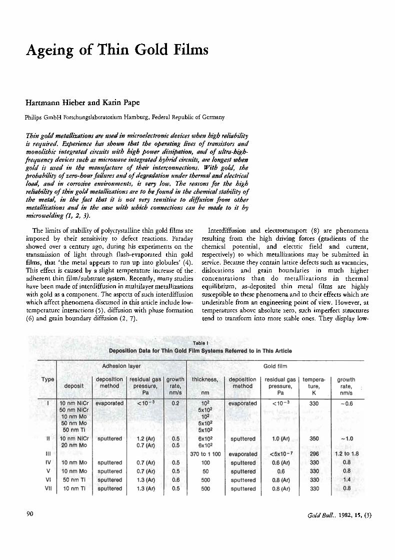
Tabla 1
Deposition Data for Thin Gold Film Systems Referred to in This Articie
Typedeposit
Adhesion layer
deposlti.ón r`esiduel gasmethod pressure
Pá
•growthrate,,nmis
thlckness,
nm
depositlonmethod
Gold film
residual gaspressure,
Pa
tempera-ture,
K
growthrate,nm/s
1 10 nm NiCr evaporated <10`3 0.2 102 èvaporated <10 -3 330 —0.650 nm NIGr 5x10210 nm Mo 10250 nm Mo 5x10250 nm Ti 5x10²
II 10 nm N`iCr sputtered 1.2 (Ar) 0.5 6x10² sputtered 1.0 (Ar) 350 —1.020 nm Mo 0.7 (Ar) 05 6x10²
III 370 to 1 100 evaporated <5x10 - 7 296 1.2 to 1.8
IV 10 nm Mo sputtered 0.7 (Ar) 0.5 100 sputtered 0.6 (Ar) 330 0.8V 10 nm Mo sputtered 0.7 (Ar) 0.5 50 sputtered 0.6 330 0.8.
VI 50 nm Ti sputtered 1.3 (Ar) 0.6 500 sputtered 0.8 (Ar) 330 1:4
VII 10 nm TI sputtered 1.3 (Ar) 0.5 500 sputtered 0.8 (Ar) 330 0.8
90 Gold Bu!!., 1982, 15, (3)
race ageing effects which are very sensitive to temperature,time and, of course, to features of the initial as-depositedstructure. Increasing knowledge of these effects has shownthat they may, in fact, be exploited to the advantage of thedesigner of electronic devices.
The purpose of this article is to review previous work and todiscuss results obtained from recent research carried out bythe authors on:(1) How different defect reactions dominate at the various
stages of ageing of thin gold films(2) The effect of ageing on important physical properties of
gold metallizations(3) Which aged metallization structures are desirable for
optimum long-term stability of thin gold films.
Sample PreparationThe substraten for the deposition of thin gold films were
p-doped silicon single crystals of <111> orientation. Theyhad the same thickness, 0.24 mm, as that used insemiconductor applications. The silicon single crystals hadbeen polished and then oxidized in a water vapour-containing atmosphere to form a silicon oxide layer 600 nmthick and of composition between SiO 1 5 and SiO 1 A . Theoxide was amorphous and showed no surface irregularitiesvisible by light interference microscopy or in transmissionelectron microscopy (TEM) of replicas. These techniqueswould have revealed a surface roughness greater than thethickness of the following adhesion layer.
Adhesion layers were deposited on the samples for recoveryexperiments. The thickness of these layers was such that theheat treatments did not cause loss of adhesion of the thingold films under investigation (9, 10). The gold films for therecrystallization experiments were evaporated withoutadhesion layers in order to avoid, at a later stage, anchoring ofgrain boundaries in them by species which diffused from theadhesion layer (11). Table I shows the deposition conditionsfor the metallizations discussed in this article.
The purity of the sputter targets and of the ingots forelectron beam evaporation was better than 99.998 weight percent. The residual gas pressures and the growth rates reportedin Table I were selected to ensure that the gold deposits had aconcentration of impurities of less than 20 ppm. Thesputtered layers contained a small amount of sputter gas(argon) trapped in grain boundaries and potes in themetallization. The films used for the recrystallizationexperiments were evaporated in ultra-high vacuum and hadan impurity level of less than 10 ppm.
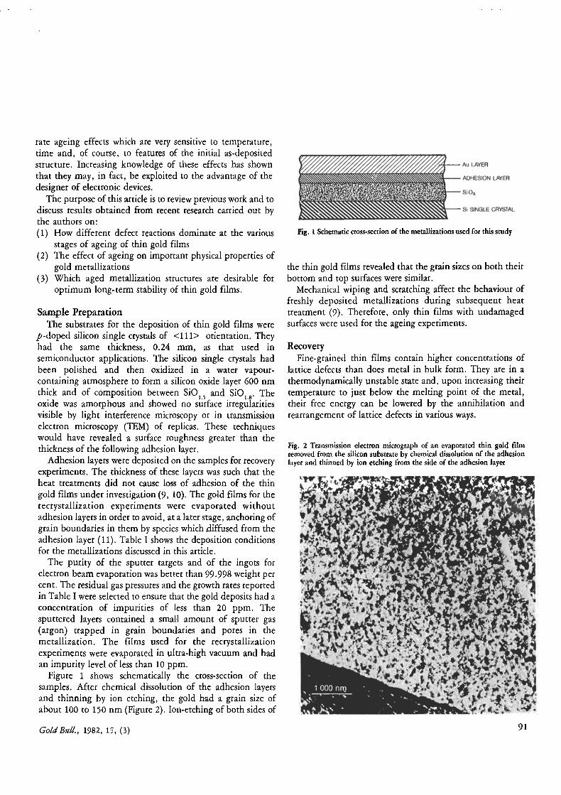
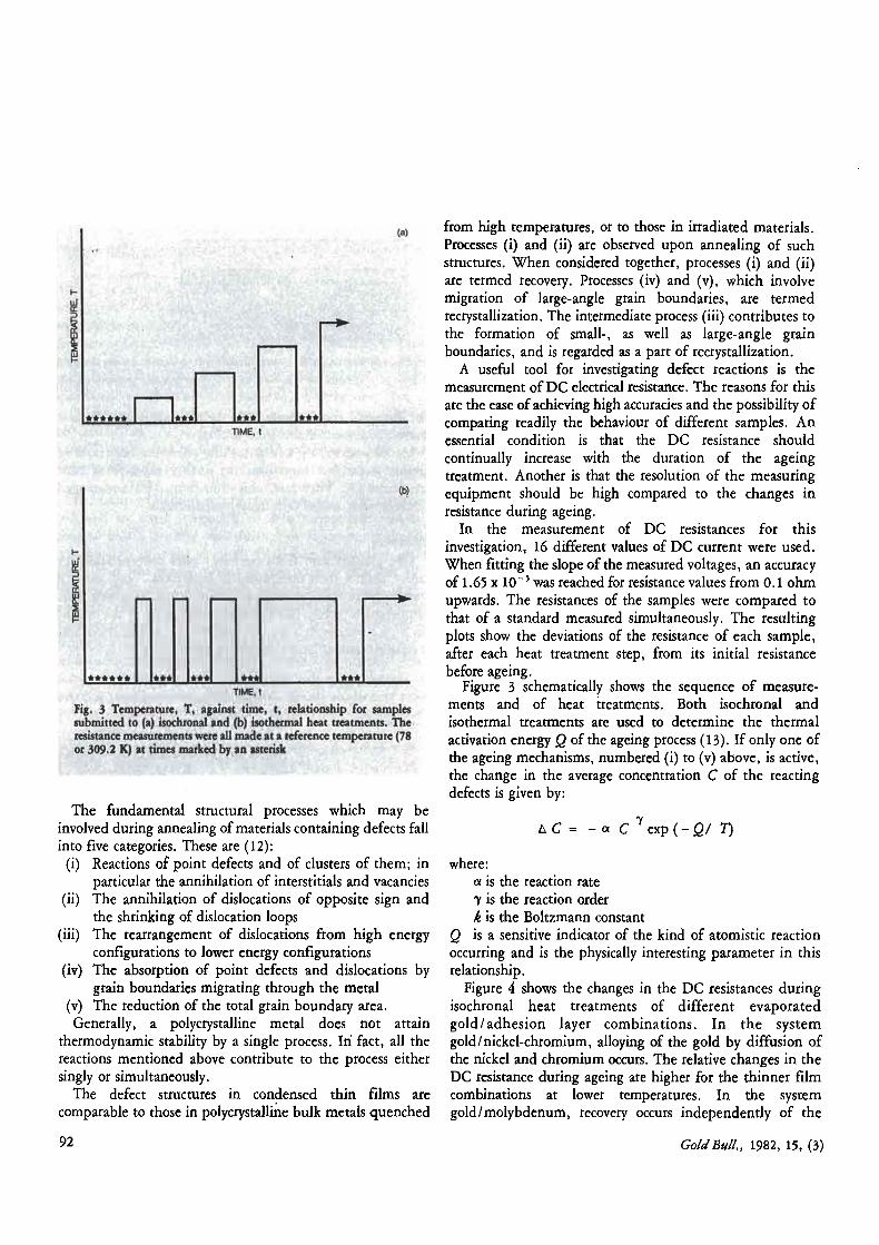
Figure 1 shows schematically the cross-section of thesamples. After chemical dissolution of the adhesion layersand thinning by ion etching, the gold had a grain size ofabout 100 to 150 nm (Figure 2). Ion-etching of both sides of
n .4 ^ ' d ^:ï^ "^,e• ris.
Fig. 1 Schematic cross-section of the metallizations used for this study
the thin gold films revealed that the grain Bizes on both theirbottom and top surfaces were similar.
Mechanical wiping and scratching affect the behaviour offreshly deposited metallizations during subsequent heattreatment (9). Therefore, only thin films with undamagedsurfaces were used for the ageing experiments.
RecoveryFine-grained thin films contain higher concentrations of
lattice defects than does metal in bulk form. They are in athermodynamically unstable state and, upon increasing theirtemperature to just below the melting point of the metal,their free energy can be lowered by the annihilation andrearrangement of lattice defects in various ways.
Fig. 2 Transmission electron micrograph of an evaporated thin gold filmremoved from the silicon substrate by chemical dissolution of the adhesionlayer and thinned by ion etching from the side of the adhesion layer
Gold Biall., 1982, U, (3) 91
TIME, t
ÛME,,t
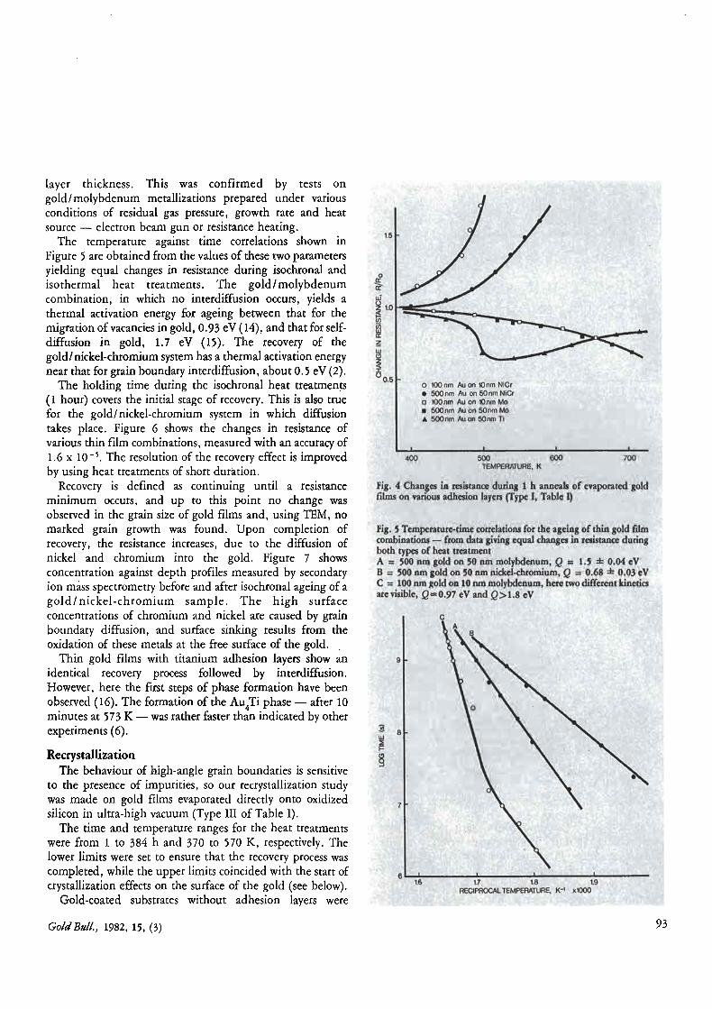
Fig, 3 Temperatu`,, To against time, : t, relationship for samplessubmitted to (a) lsqchio .and' (b) isothermal heat treatments. Theresistance measurements were all made .at a réference temperature (78ór 309.2 IK) at eimes matkè• by, an asterisk .
The fundamental structural processes which may beinvolved during annealing of materials containing defects fallinto five categories. These are (12):
(i) Reactions of point defects and of clusters of them; inparticular the annihilation of interstitials and vacancies
(ii) The annihilation of dislocations of opposite sign andthe shrinking of dislocation loops
(iii) The rearrangement of dislocations from high energyconfigurations to lower energy configurations
(iv) The absorption of point defects and dislocations bygram boundaries migrating through the metal
(v) The reduction of the total gram boundary area.Generally, a polycrystalline metal does not attain
thermodynamic stability by a single process. In fact, all thereactions mentioned above contribute to the process eithersingly or simultaneously.
The defect structures in condensed thin films arecomparable to those in polycrystalline bulk metals quenched
from high temperatures, or to those in irradiated materials.Processes (i) and (ii) are observed upon annealing of suchstructures. When considered together, processes (i) and (ii)are termed recovery. Processes (iv) and (v), which involvemigration of large-angle grain boundaries, are termedrecrystallization. The intermediate process (iii) contributes tothe formation of small-, as well as large-angle gramboundaries, and is regarded as a part of recrystallization.
A useful tool for investigating defect reactions is themeasurement of DC electrical resistance. The reasons for thisare the ease of achieving high accuracies and the possibility ofcomparing readily the behaviour of different samples. Anessential condition is that the DC resistance shouldcontinually increase with the duration of the ageingtreatment. Another is that the resolution of the measuringequipment should be high compared to the changes inresistance during ageing.
In the measurement of DC resistances for thisinvestigation, 16 different values of DC current were used.When fitting the slope of the measured voltages, an accuracyof 1.65 x 10 was reached for resistance values from 0.1 ohmupwards. The resistances of the samples were compared tothat of a standard measured simultaneously. The resultingplots show the deviations of the resistance of Bach sample,after each heat treatment step, from its initial resistancebefore ageing.
Figure 3 schematically shows the sequence of measure-ments and of heat treatments. Both isochronal andisothermal treatments are used to determine the thermalactivation energy Q of the ageing process (13). If only one ofthe ageing mechanisms, numbered (i) to (v) above, is active,the change in the average concentration C of the reactingdefects is given by:
L,C= —a C ry exp(—Q/ 7)
where:« is the reaction rate-y is the reaction orderk is the Boltzmann constant
Q is a sensitive indicator of the kind of atomistic reactionoccurring and is the physically interesting parameter in thisrelationship.
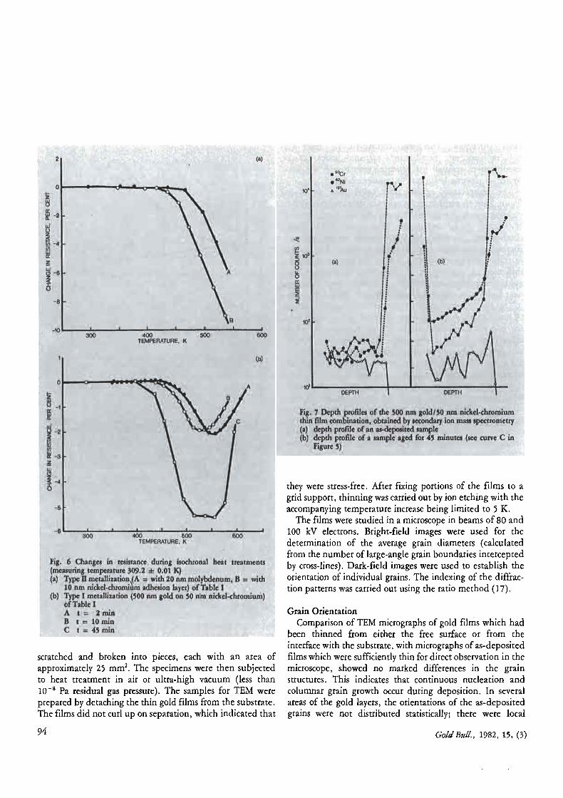
Figure 4 shows the changes in the DC resistances duringisochronal heat treatments of different evaporatedgold/adhesion layer combinations. In the systemgold/nickel-chromium, alloying of the gold by diffusion ofthe nekel and chromium occurs. The relative changes in theDC resistance during ageing are higher for the thinner filmcombinations at lower temperatures. In the systemgold/molybdenum, recovery occurs independently of the
92 Gold Bull., 1982, 15, (3)
1.5
4Ç 0 700EMPERATLfRE, K
F g: 4 Ghan,^es in, >;eaistancc.c urmg t h anneals of evaporated - go dfilms oo'varieua 3 esion Jay hype I, Table ï)
Fig -5 Tempetature-thhne oor ela lons for .the ageing of thin gold filmcombïnatïbas — Erom data giving oqual chánges'iirresistance duringbotte types o Beat uc tmentA =. 500 nai gold on 50 bin molybdénum 7 = 1'.} ±'U 04 cYB = 500 om gol4.oh 50 om nickcl-çhtonuwn Q . = 068 11;03 eVC = 100 om gold uu 10 nn molybdenum, here two different Jkïneticsare yisible, Q-0.97 ëV and Q.>i.8 eV
UJ
7.6: 1.FF ._. _..'Lg.... ._ 1.9RECIPROCALTEMPERATURE, K-' xf000
layer thickness. This was confirmed by tests ongold/molybdenum metallizations prepared under variousconditions of residual gas pressure, growth rate and heatsource — electron beam gun or resistance heating.
The temperature against time correlations shown inFigure 5 are obtained from the valnes of these two parametersyielding equal changes in resistance during isochronal andisothermal heat treatments. The gold/molybdenumcombination, in which no interdiffusion occurs, yields athermal activation energy for ageing between that for themigration of vacancies in gold, 0.93 eV (14), and that for self-diffusion in gold, 1.7 eV (15). The recovery of thegold/ nickel-chromium system has a thermal activation energynear that for grain boundary interdiffusion, about 0.5 eV (2).
The holding time during the isochronal heat treatments(1 hour) covers the initial stage of recovery. This is also truefor the gold/nickel-chromium system in which diffusiontakes place. Figure 6 shows the changes in resistance ofvarious thin film combinations, measured with an accuracy of1.6 x 10 - s. The resolution of the recovery effect is improvedby using heat treatments of short duration.
Recovery is defined as continuing until a resistanceminimum occurs, and up to this point no change wasobserved in the grain size of gold films and, using TEM, nomarked grain growth was found. Upon completion ofrecovery, the resistance increases, due to the diffusion ofnickel and chromium into the gold. Figure 7 showsconcentration against depth profiles measured by secondaryion mass spectrometry before and after isochronal ageing of agold/nickel-chromium sample. The high surfaceconcentrations of chromium and nickel are caused by grainboundary diffusion, and surface sinking results from theoxidation of these metals at the free surface of the gold.
Thin gold films with titanium adhesion layers show anidentical recovery process followed by interdiffusion.However, here the first steps of phase formation have beenobserved (16). The formation of the Au 4Ti phase — after 10minutes at 573 K — was rather faster than indicated by otherexperiments (6).
RecrystallizationThe behaviour of high-angle grain boundaries is sensitive
to the presence of impurities, so our recrystallization studywas made on gold films evaporated directly onto oxidizedsilicon in ultra-high vacuum (Type III of Table I).
The time and temperature ranges for the heat treatmentswere from 1 to 384 h and 370 to 570 K, respectively. Thelower limits were set to ensure that the recovery process wascompleted, while the upper limits coincided with the start ofcrystallization effects on the surface of the gold (see below).
Gold-coated substrates without adhesion layers were
z
o. 100.nm: Man ;l4nm:MICt9``5ÓOnm Au on 50nin NiG.
1OOnm M'cá 1onrn Ma11 5Om A^ ón SOnm'.Mo1 5Ónm Au.br+ 5dnm D
Gold Bull., 1982, 15, (3) 93
1'lg. 6 Change. in wsistance-, dtin-ij kochnonûl keát Ireatlneotstnëasuxing tempegiture 309.2 0,01K)á)'. qpe fl in ta1Iizanonl(AL wtth 20 em lnoly denum, b witli
10 tuu nekel chromium a lheston Iayer} of l abié 1(bl, iype 1 met i lizat on 1500 !un galj on 50 nnl° jurk oimiw ►}
t c l0 ruinC C = •45 initi
scratched and broken into pieces, Bach with an area ofapproximately 25 mm'. The specimens were then subjectedto heat treatment in air or ultra-high vacuum (less than10 - s Pa residual gas pressure). The samples for TEM wereprepared by detaching the thin gold films from the substrate.The films did not curl up on separation, which indicated that
94
Fig.. 1. Depth ,rpfiles otTle 500 pns;.oldi.9 un.hçkè1-kromium. .thini ¢Ly combinactoit ,; btaa►ed by se ondary ton mais s euroníetry.(a)' s'pth ,pr ë tf an as aepostted aa i€( 4pt p5° le a : amp e ag Ifo 45 àiinatel (se® cuFe C in.
Figurë S)
they were stress-free. After fixing portions of the films to agrid support, thinning was carried out by ion etching with theaccompanying temperature increase being limited to 5 K.
The films were studied in a microscope in beams of 80 and100 kV electrons. Bright-field images were used for thedetermination of the average grain diameters (calculatedfrom the number of large-angle grain boundaries interceptedby cross-lines). Dark-field images were used to establish theorientation of individual grains. The indexing of the diffrac-tion patterns was carried out using the ratio method (17).
Grain OrientationComparison of TEM micrographs of gold films which had
been thinned from either the free surface or from theinterface with the su bstrate, with micrographs of as-depositedfilms which were sufciently thin for direct observation in themicroscope, showed no marked differences in the grainstructures. This indicates that continuous nucleation andcolumnar grain growth occur during deposition. In severalareas of the gold layers, the orientations of the as-depositedgrains were not distributed statistically; there were local
Gold Bull., 1982, 15, (3)
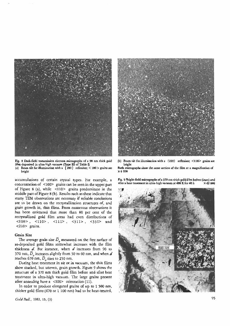
Fig. 8 Dark-field transmission electron micrographs of a 90 nm thick goldfilm deposited in ultra-high vacuum (Type III of Table I)(a) Beam tilt for illumination witha { 200 } reflexion; <100> grains are
bright
accumulations of certain crystal types. For example, aconcentration of <100> grains can be seen in the upper partof Figure 8 (a), while <110> grains predominate in themiddle part of Figure 8 (b). Results such as these indicate thatmany TEM observations are necessary if reliable conclusionsare to be drawn on the recrystallization structures of, andgram growth in, thin films. From numerous observations itbas been estimated that more than 80 per cent of therecrystallized gold film areas had even distributions of<100> , <110> , <111> , <311> , <331> and<210> grains.
Grain SizeThe average graïn size Da measured on the free surface of
as-deposited gold films somewhat increases with the filmthickness _d. For instante, when d increases from 90 to370 nm, Do increases slightly from 50 to 60 nm, and when dreaches 670 nm, DQ rises to 250 nm.
During heat treatment in air or in vacuum, the thin filmsshow marked, but uneven, gram growth. Figure 9 shows thestructure of a 370 nm thick gold film before and after heattreatment in ultra-high vacuum. The large grains presentafter annealing have a <100> orientation (11).
In order to produce elongated grains of up to 1 500 nm,thicker gold films (670 or 1 100 nm) had to be heat-treated,
(b) Beam tilt for illumination with a (220) reflexion; <110> grains arebright
Both micrographs show the same section of the film at a magnification ofx4 000
Fig. 9 Bright-field micrographs of a 370 nm thick gold film before (inset) andafter a heat treatment in ultra-high vacuum at 480 K for 40 h x 42 000
Gold Bull., 1982, 15, (3) 95
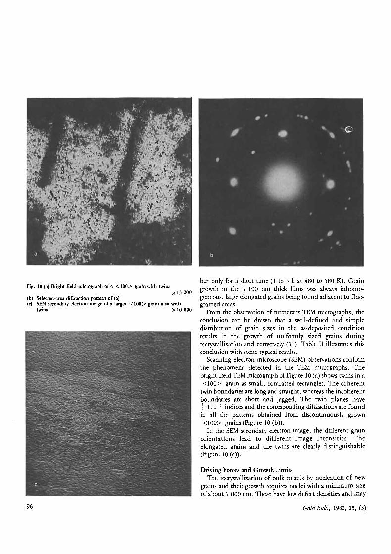
Fig. 10 (a) Bright-field micrograph of a <100> grain with twinsX 13 200
(b) Selected-area diffraction pattern of (a)(c) SEM secondary electron image of a larger <100> gram also with
twins X 10 000
but only for a short time (1 to 5 h at 480 to 580 K). Graíngrowth in the 1 100 nm thick films was always inhomo-geneous, large elongated grains being found adjacent to fine-grained areas.
From the observation of numerous TEM micrographs, theconclusion can be drawn that a well-defined and simpledistribution of gram sizes in the as-deposited conditionresults in the growth of uniformly sized grains duringrecrystallization and conversely (11). Table II illustrates thisconclusion with some typical results.
Scanning electron microscope (SEM) observations confirmthe phenomena detected in the TEM micrographs. Thebright-field TEM micrograph of Figure 10 (a) shows twins in a<100> gram as small, contrasted rectangles. The coherent
twin boundaries are long and straight, whereas the incoherentboundaries are short and jagged. The twin planes have{ 111 } indices and the corresponding diffractions are foundin all the patterns obtained from discontinuously grown<100> grains (Figure 10 (b)).
In the SEM secondary electron image, the different gramorientations lead to different image intensities. Theelongated grains and the twins are clearly distinguishable(Figure 10 (c)).
Driving Forces and Growth LimitsThe recrystallization of bulk metals by nucleation of new
grains and their growth requires nuclei with a minimum sizeof about 1 000 nm. These have low defect densities and may
96 Gold Bull., 1982, 15, (3)
7étaI II ,
lypfcaI Qrain Sïzes of Thin QOT,d,' Fifrimsyp® IIIQ áf Tabre i) àfterNeài Treátments
^i^lim^ I .. kreaRrt?iért^cl rtiesa, feniperaluf
tratf-cent Grel $tze., irnmuns,h` fnfn. .ave max
48 11 130: :50 s o ,1 3 0 0: i19Ó
25; á5Q°40i 6 11I 25 X00.,'570 5 110 50 900370 1Ga 10 50 99`, :.450 168. 1 Q I0°570 34 100 0. 1 400^.. —
1W : `.j 9 Q ,
370 — 800.480 1: — 20>505057 — kgb . 15OI90 =480 9
— 170 1061`—
370. 16 — 24P =25000480 180' — lOIP —501670 168 — 1`'610 ` _ .50Q
so.
670
form as a result of grain boundary migration into grains withhigh defect densities (18). The thin gold films discussed herehad initial grain sizes which were much smaller (Table II).
Nucleation of new grains is not required forrecrystallization which may also occur by grain growth alone.This is indeed what we observed in thin gold films. However,the mechanism of grain growth has not yet been modelledquantitatively (19) and only qualitative experimental data areavailable concerning the dependence of grain boundarymobility on the driving forces produced by different kinds oflattice defects.
The forces driving or retarding grain boundary movementin thin gold films are listed in Table III. The annihilation ofdislocations and the reduction of the grain boundary area perunit volume are the most effective_ driving forces. Themaximum recrystallization grain size Dijm is determined bythe equilibrium between these two driving forces and theretarding force due to surface grooving (Table I11) yielding:
Dlim = 12d
Table IV shows the maximum grain sizes observed by us tobe comparable with this estimated value.
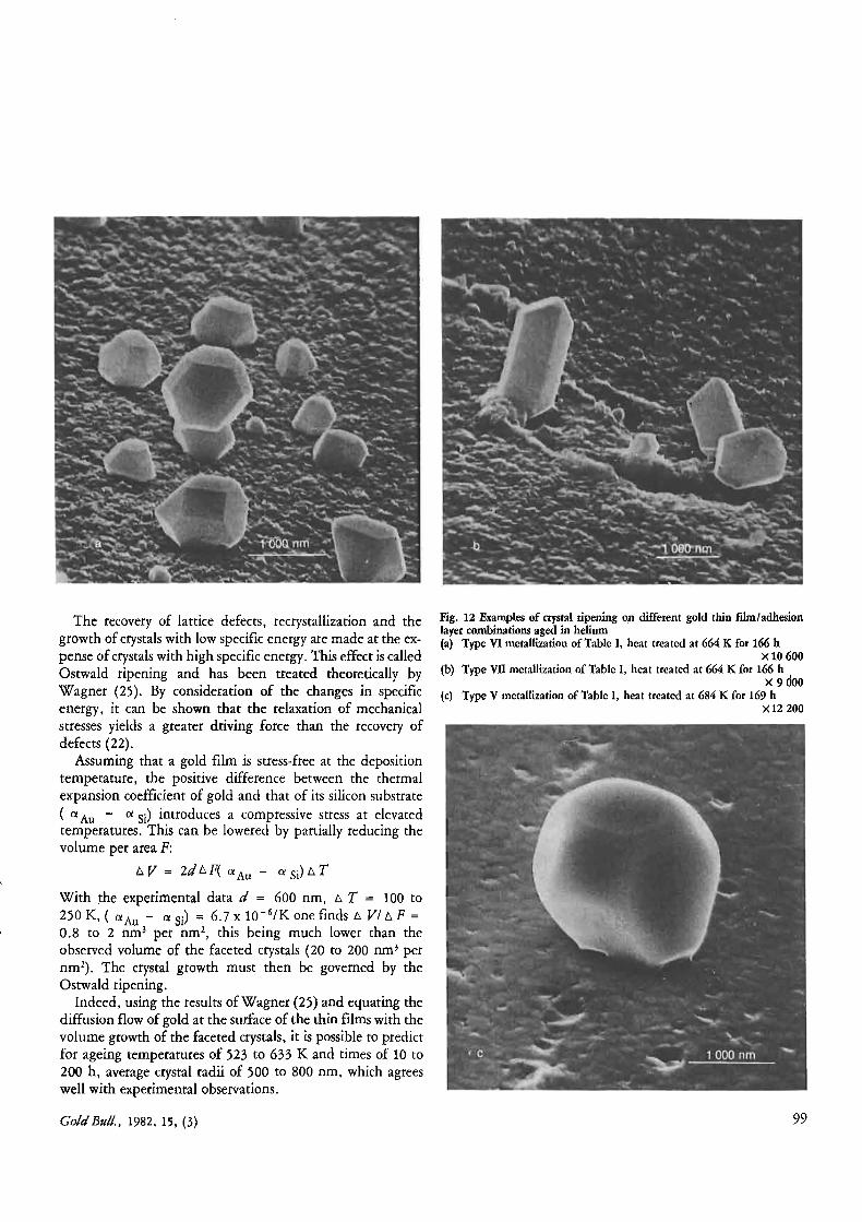
Crystal RipeningHeat treatment of thin gold films at elevated temperatures
and for several days leads to the formation of gold crystalliteson their surfaces. Figure 11 shows how this phenomenoncharacteristically begins with local thickening and poreformation in a gold/molybdenum metallization. Thematerial which is necessary for the local thickening migrates
Tabla, Hi"
Fot'ces Driving Or Retarding'the Mohon pf a Grairk BOu idarlr
Cau'sé,of Parár00 e 9 va'lues [ 1iir1 t ' R ardirig'Formgla , ' 7 t00s foroe,,
the force for gójd t f Ilm N/n5?
1: deformatiorenergy
2. GB energy
3. difference In surface energy.of adjacent grains
4..thermaiiy Indopedmechanica) stress
5. surface grooving
p = driving/retarding force, p = densit
pO__ dQ3011109,nm
2E 'i 0O Kè
d O.to i 100,nm
y, -r - mechanica) stress, 6 - elastjcitg rnod lusr d = k
^1Q^^t?^.10s
1f1^ RC 1fi^s
I'nl h'igkness
i:de rdr 165
p =PUC`
p=37 oè- D,
p1011 fp.
D - 6dte.1!Qnr
Gold Bull., 1982, 15, (3) 97
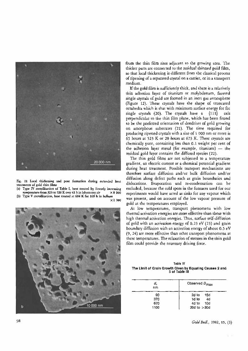
Fig. 11 Local thickening and pore formation during extended heattreatments of gold thin films(a) Type IV metaffization of Table I, heat treated by linearly increasing
temperature from 323 to 526 K over 41 h in laboratory air X 8 000(b) Type V metallization, heat treated at 684 K for 169 h in helium
X2 300
from the thin film sites adjacent to the growing area. Thethicker parts are connected to the residual thinned gold film,so that local thickening is different from the classical processof ripening of a separated crystal on a carrier, or in a transportmedium.
If the gold film is sufficiently thick, and there is a relativelythin adhesion layer of titanium or molybdenum, facetedsingle crystals of gold are formed in an inert gas atmosphere(Figure 12). These crystals have the shape of truncatedoctahedra which is that with minimum surface energy for fccsingle crystals (20). The crystals have a {111} axisperpendicular to the thin film plane, which has been foundto be the preferred orientation of dendrites of gold growingon amorphous substrates (21). The time required forproducing ripened crystals with a size of 1 000 nm or more is65 hours at 523 K or 20 hours at 673 K. These crystals arechemically pure, containing less than 0.1 weight per cent ofthe adhesion layer metal (for example, titanium) — theresidual gold layer contains the diffused species (22).
The thin gold films are not subjected to a temperaturegradient, an electric current or a chemical potential gradientduring heat treatment. Possible transport mechanisms aretherefore surface diffusion and/or bulk diffusion and/ordiffusion along defect paths such as grain boundaries anddislocations. Evaporation and re-condensation can beexcluded, because the cold spots in the furnaces used for ourexperiments would have acted as sinks for any vapour whichwas present, and on account of the low vapour pressure ofgold at the temperatures employed.
At low temperatures, transport phenomena with lowthermal activation energies are more effective than those withhigh thermal activation energies. Thus, surface self-diffusionof gold with an activation energy of 0.23 eV (23) and grainboundary diffusion with an activation energy of about 0.5 eV(9, 24) are more effective than other transport phenomena atthese temperatures. The relaxation of stresses in the thin goldfilm could provide the necessary driving force.
Table IV
The Limit of Grain Growth Given by Equating Causes 2 and5 of Table III
d, Observed Dmaxnm
90 2d to 15d370 i d to 4d670 4d to 10d
1100 20d to >30d
98 Gold Bull., 1982, 15, (3)
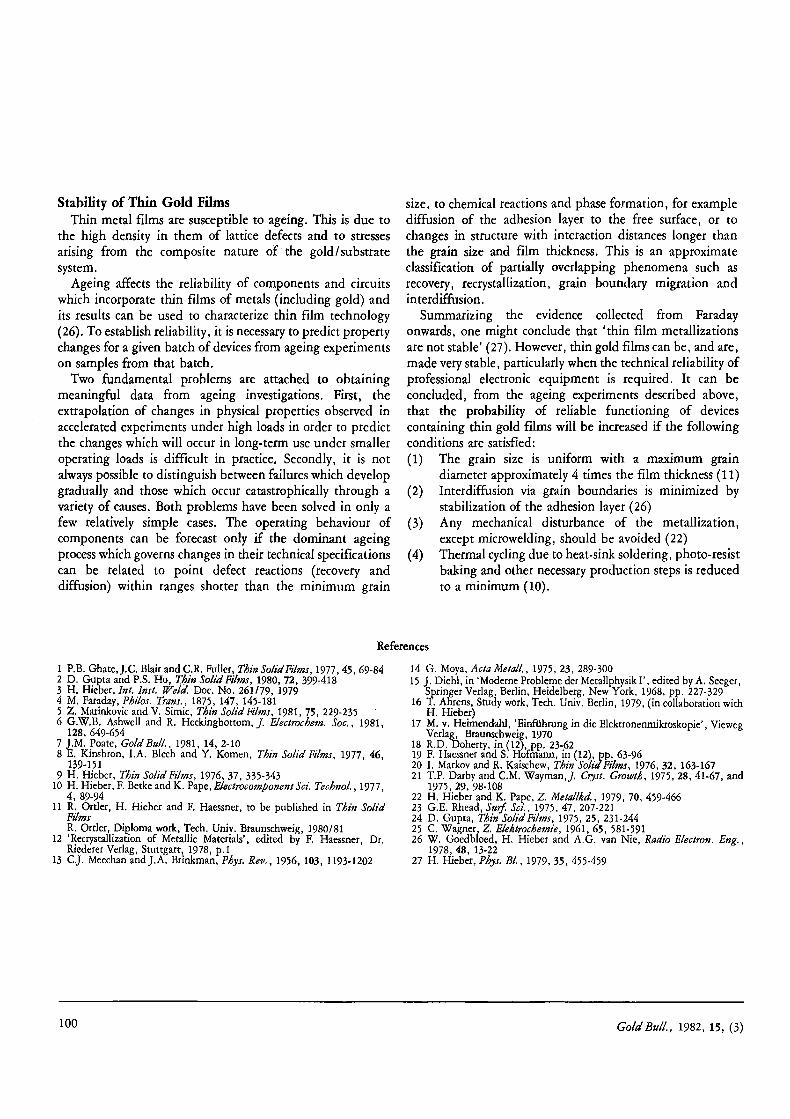
The recovery of lattice defects, recrystallization and thegrowth of crystals with low specific energy are made at the ex-pense of crystals with high specific energy. This effect is calledOstwald ripening and has been treated theoretically byWagner (25). By consideration of the changes in specificenergy, it can be shown that the relaxation of mechanicalstresses yields a greater driving force than the recovery ofdefects (22).
Assuming that a gold film is stress-free at the depositiontemperature, the positive difference between the thermalexpansion coefficient of gold and that of its Bilicon substrate( aAu — u si) introduces a compressive stress at elevatedtemperatures. This can be lowered by partially reducing thevolume per area F:
LV = 2dLF( elAu — asi)L, T
With the experimental data d = 600 nm, o T = 100 to250 K, (a Au — a Si) = 6.7 x 10 - '/ K one finds o VI o F =0.8 to 2 nm 3 per nm 2, this being much lower than theobserved volume of the faceted crystals (20 to 200 nm 3 pernm 2). The crystal growth must then be governed by theOstwald ripening.
Indeed, using the results of Wagner (25) and equating thediffusion flow of gold at the surface of the thin films with thevolume growth of the faceted crystals, it is possible to predictfor ageing temperatures of 523 to 633 K and times of 10 to200 h, average crystal radii of 500 to 800 nm, which agreeswell with experimental observations.
Fig. 12 Examples of crystal ripening on different gold thin film/adhesionlayer combinations aged in helium(a) Type VI inetallization of Table I, heat treated at 664 K for 166 h
x 10 600(b) Type VII metallization of Table I, heat treated at 664 K for 166 h
X 9 000(c) Type V metallization of Table I, heat treated at 684 K for 169 h
X12 200
Gold Bull., 1982, 15, (3) 99
Stability of Thin Gold FilmsThin metal films are susceptible to ageing. This is due to
the high density in them of lattice defects and to stressesarising from the composite nature of the gold/substratesystem.
Ageing affects the reliability of components and circuitswhich incorporate thin films of metals (including gold) andits results can be used to characterize thin film technology(26). To establish reliability, it is necessary to predict propertychanges for a given batch of devices from ageing experimentson samples from that batch.
Two fundamental problems are attached to obtainingmeaningful data from ageing investigations. First, theextrapolation of changes in physical properties observed inaccelerated experiments under high loads in order to predictthe changes which will occur in long-term use under smalleroperating loads is difficult in practice. Secondly, it is notalways possible to distinguish between failures which developgradually and those which occur catastrophically through avariety of causes. Both problems have been solved in only afew relatively simple cases. The operating behaviour ofcomponents can be forecast only if the dominant ageingprocess which governs changes in their technical specificationscan be related to point defect reactions (recovery anddiffusion) within ranges shorter than the minimum grain
size, to chemical reactions and phase formation, for examplediffusion of the adhesion layer to the free surface, or tochanges in structure with interaction distantes longer thanthe grain size and film thickness. This is an approximateclassification of partially overlapping phenomena such asrecovery, recrystallization, grain boundary migration andinterdiffusion.
Summarizing the evidente collected from Faradayonwards, one might conclude that 'thin film metallizationsare not stable' (27). However, thin gold films can be, and are,made very stable, particularly when the technical reliability ofprofessional electronic equipment is required. It can beconcluded, from the ageing experiments described above,that the probability of reliable functioning of devicescontaining thin gold films will be increased if the followingconditions are satisfied:(1) The grain size is uniform with a maximum grain
diameter approximately 4 times the film thickness (11)(2) Interdiffusion via grain boundaries is minimized by
stabilization of the adhesion layer (26)
(3) Any mechanical disturbance of the metallization,except microwelding, should be avoided (22)
(4) Thermal cycling due to heat-sink soldering, photo-resistbaking and other necessary production steps is reducedto a minimum (10).
References
1 P.B. Ghate, J.C. Blair and C.R. Fuller, Thin Solid Films, 1977, 45, 69-842 D. Gupta and P.S. Ho, Thin Solid Films, 1980, 72, 399-4183 H. Hieber, Int, Inst, Wei.. Doe. No. 261/79, 19794 M. Faraday, Phrlos. Trans., 1875, 147, 145-1815 Z. Marinkovic and V. Simic, Thin Solid Films, 1981, 75, 229-2356 G.W.B. Ashwell and R. Heekingbottom, J. Elecirochem. Soc., 1981,
128,649-6547 J.M. Poate, GoldBull., 1981, 14, 2-108 . Kinsbron, I.A. Blech and Y. Komen, Thin Solid Films, 1977, 46,
139-1519 H. Hieber, Thin Solid Films, 1976, 37, 335-343
10 H. Hieber, F. Betke and K. Pape, Electrocomponent Sci. Technol., 1977,4, 89-94
11 R. Ortler, H. Hieber and F. Haessner, to be published in Thin SolidFilmsR. Ortler, Diploma work, Tech. Univ. Braunschweig, 1980/81
12 'Recrystallization of Metallic Materials', edited by F. Haessner, Dr.Riederer Verlag, Stuttgart, 1978, p.1
13 C.J. Meethan and J.A. Brinkman, Phys. Rep., 1956, 103, 1193-1202
14 G. Moya, Acta Me/all., 1975, 23, 289-30015 J. Diehl, in 'Moderne Probleme der Metallphysik I', edited by A. Seeger,
Springer Verlag, Berlin, Heidelberg, New York, 1968, pp. 227-32916 '1. Ahrens, Study work, Tech. Univ. Berlin, 1979, (in collaboration with
H. Hieber)17 M. v. Heimendahl, 'Einfihrung in die Elektronenmikroskopie', Vieweg
Verlag, Braunschweig, 197018 R.D. Doherty, in (12), pp. 23-6219 F. Haessner and S. Hofmann, in (12), pp. 63-9620 I. Markov and R. Kaischew, Thin Solid Films, 1976, 32, 163-16721 T.P. Darby and C.M. Wayman, J, Cryst. Growth, 1975, 28, 41-67, and
1975, 29, 98-10822 H. Hieber and K. Pape, Z. Metallkd., 1979, 70, 459-46623 G.E. Rhead, Surf SGY„ 1975, 47, 207-22124 D. Gupta, Thin Solid Films, 1975, 25, 231-24425 C. Wagner, Z. Elektrochemie, 1961, 65, 581-59126 W. Goedbloed, H. Hieber and A.G. van Nie, Radio Electron. Eng.,
1978, 48, 13-2227 H. Hieber, Phys. BI., 1979, 35, 455-459
100 Gold Bull., 1982, 15, (3)