Embed Size (px)
Citation preview
MYD-LPC1788 User Manual
MYD-LPC1788 User
Manual Version V1.3
MYD-LPC1788 User Manual
Version History
Version
Number
Description Time
V1.0 Initial Version 2012.09.14
V1.1 Adjust the list of product configuration 2012.11.02
V1.2 Add 7.0-inch screen support) 2013.02.22
V1.3 modify the contact information 2013.03.28
MYD-LPC1788 User Manual
Directory
Chapter 1 Product Overview ............................................................................................... 1
1.1 Product Description ................................................................................................ 1
1.2 Product Preview ..................................................................................................... 1
1.3 Product Features .................................................................................................... 2
1.4 Product Configuration ............................................................................................. 4
Chapter 2 Hardware Resource Introduction ........................................................................ 5
2.1Hardware Resource Overview ................................................................................ 5
2.2 Main Module Introduction ....................................................................................... 6
2.2.1 Main processor LPC1788 ............................................................................ 6
2.2.2 SDRAM Module ........................................................................................... 6
2.2.3 SRAM Module .............................................................................................. 7
2.2.4 NORFLASH Module ..................................................................................... 8
2.2.5 SPI FLASH Module ...................................................................................... 9
2.2.6 EEPROM Module ....................................................................................... 10
2.2.7Ethernet MAC Module ................................................................................. 11
2.2.8Audio Module .............................................................................................. 12
2.2.9 Touch Controller Module ............................................................................ 13
2.2.10User Key and Reset Circuit ....................................................................... 14
2.2.11 Buzzer ...................................................................................................... 14
2.2.12 LED .......................................................................................................... 15
2.3 Peripheral Interface introduction .......................................................................... 15
2.3.1 UART Interface ........................................................................................... 15
2.3.2 CAN Interface ............................................................................................. 16
2.3.3 RS485 Interface ......................................................................................... 16
2.3.4 SDCARD Interface ..................................................................................... 17
2.3.5 USB OTG/HOST interface ......................................................................... 17
2.3.6 JTAG interface............................................................................................ 19
MYD-LPC1788 User Manual
2.3.7 LCD Touch Screen Interface ...................................................................... 19
2.3.8 User Interface ............................................................................................. 20
2.3.9 ADC and DAC Interface ............................................................................. 20
2.4Jumper setting ....................................................................................................... 21
Chapter 3 MDK Routine ..................................................................................................... 23
3.1 Overview ............................................................................................................... 23
3.2 Preparation ........................................................................................................... 23
3.2.1 Configure and CompileMDK Routine ......................................................... 23
3.2.2 DebugMDK Routine ................................................................................... 26
3.2.3Download programby ULINK2 .................................................................... 28
3.2.4 ISP Download............................................................................................. 31
3.3MDK source use .................................................................................................... 35
3.3.1 Directory structure ...................................................................................... 35
3.3.2 Add function module................................................................................... 36
3.3.3Use Printf ..................................................................................................... 37
3.4 The introduction of MDK routine........................................................................... 39
3.4.1 ADC_Interrupt ............................................................................................ 39
3.4.2 ADC_Polling ............................................................................................... 40
3.4.3 CAN_Test ................................................................................................... 41
3.4.4 Crc_Demo .................................................................................................. 42
3.4.5 Dac_Dma ................................................................................................... 43
3.4.6 Dac_SineWave ........................................................................................... 44
3.4.7 DMA_Flash2Ram ....................................................................................... 44
3.4.8 Eeprom_Demo ........................................................................................... 45
3.4.9 Emc_NorFlashDemo .................................................................................. 46
3.4.10 Emc_SdramDemo .................................................................................... 47
3.4.11 Emc_SramDemo ...................................................................................... 47
3.4.12 GPIO_Interrupt ......................................................................................... 48
3.4.13 GPIO_LedBlinky ....................................................................................... 49
MYD-LPC1788 User Manual
3.4.14 Nvic_VectorTableRelocation .................................................................... 49
3.4.15 Pwm_SingleEdge ..................................................................................... 50
3.4.16 Pwm_DualEdge ....................................................................................... 50
3.4.17 Pwm_MatchInerrupt ................................................................................. 51
3.4.18 PWR_Sleep .............................................................................................. 52
3.4.19 PWR_DeepSleep ..................................................................................... 53
3.4.20 Emac_EasyWeb ....................................................................................... 53
3.4.21 Rtc_Alarm................................................................................................. 54
3.4.22 SSP_Touchscreen.................................................................................... 55
3.4.23 SSP_Flash ............................................................................................... 56
3.4.24 Systick_100msBase ................................................................................. 57
3.4.25Timer_MatchInterrupt ................................................................................ 57
3.4.26 Wdt_Interrupt............................................................................................ 58
3.4.27 Wdt_Reset ................................................................................................ 59
3.4.28 Lcd_LQ043T3DX0A ................................................................................. 60
3.4.29Lcd_touch .................................................................................................. 60
3.4.30 Mci_CidCard ............................................................................................ 60
3.4.31 Usb_MassStorage .................................................................................... 61
3.4.32 Usb_VirtualCom ....................................................................................... 62
3.4.33 I2S_Audio ................................................................................................. 63
3.4.34 I2C_Eeprom ............................................................................................. 64
3.4.35 RS_485-Master&Slave ............................................................................ 65
Appendix 1sales FAQ and technical support..................................................................... 67
1
MYD-LPC1788 User Manual
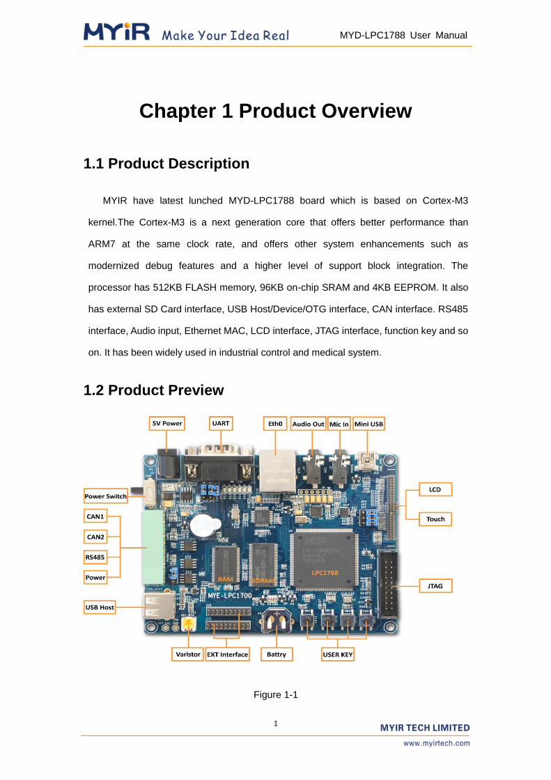
Chapter 1 Product Overview
1.1 Product Description
MYIR have latest lunched MYD-LPC1788 board which is based on Cortex-M3
kernel.The Cortex-M3 is a next generation core that offers better performance than
ARM7 at the same clock rate, and offers other system enhancements such as
modernized debug features and a higher level of support block integration. The
processor has 512KB FLASH memory, 96KB on-chip SRAM and 4KB EEPROM. It also
has external SD Card interface, USB Host/Device/OTG interface, CAN interface. RS485
interface, Audio input, Ethernet MAC, LCD interface, JTAG interface, function key and so
on. It has been widely used in industrial control and medical system.
1.2 Product Preview
Figure 1-1
2
MYD-LPC1788 User Manual
1.3 Product Features
Based on Cortex-M3 processor, MYD-LPC1788 integrates all the chip functions and
features. The main features are as follows:
Electrical parameters
Operating Temperature : -40℃~85℃
Electrical Specifications: +5V power supply
Mechanical Dimensions: 115mmx90mm
Processor
LPC1788(Cortex-M3 kernel), runs at up to 120MHz
96KB on-chip SRAM
512KB on-chip ROM
4KB on-chip EEPROM
Memory
32MB SDRAM
1MB SRAM
2MB NORFLASH
256B EEPROM
4MB SPI FLASH
Audio and Video Interface
An Audio 3.5mm Input Interface
A Two-channel Audio 3.5mm Output Interface
LCD Touch-Screen Interface
24 True Color
Resolution: Support up to 1024 x 768
Transmission Interface
One serial(select UART0/UART2 by jumper)
One high-speed USB HOST interface
One mini USB interface
3
MYD-LPC1788 User Manual
One Ethernet MAC.
Two CAN Interface
One RS485 Interface
Input interface
Standard JTAG Interface
MicroSD Card Interface
LED indicator
One system power indicator(red)
Applications
Communications
Point-of-sale terminals, Web servers, multi-protocol bridges
Industrial/Medical
Automation controllers, application control, robotic controls, HVAC, PLC,
inverters, circuit breakers, medical scanning, security monitoring, motor
drive, video intercom.
Consumer/Appliance
Audio, MP3 decoders, alarm systems, displays, printers, scanners, small
appliances, fitness equipment
Automotive
Aftermarket, car alarms, GPS/Fleet Monitor
4
MYD-LPC1788 User Manual
1.4 Product Configuration
NO Name Number Note
1 MYD LPC1788 Development Board 1
2 1.5 Meters Crossover Cable 1
3 1.5 Meters high-speed Mini USB 2.0
Cable 1
4 9Pin to 9Pin serial cable 1
5 DVD Product 1
Include Schematic (PDF),
User Manual, Source Code,
etc.
6 4.3/7.0 Inch LCD Touch Screen 1 optional
Table 1-1
5
MYD-LPC1788 User Manual
Chapter 2 Hardware Resource
Introduction
2.1Hardware Resource Overview
MYD-LPC1788 resources are shown in table2-1:
Item Feature
Size Board size:115mm x 90mm
CPU LPC1788(Cortex-M3 Core), Up to 120MHz
Memory
On-chip: 96KB SRAM,512KB ROM, 4KB EEPROM
External: 32MB SDRAM, 1MB SRAM, 2MB NORFLASH, 256B
EEPROM, 4MB SPI FLASH
Debug 20 Pin, 2.54mm JTAG debug interface
Peripheral
Type Quantity Description
RS485 1 Support RS485
Ethernet 1 100Mbps,DP83848
CAN 2 Support CAN
USB 2
Support USB
HOST/Device 2.0
USBOTG 2.0
Audio 2 Audio in/out
SD interface 1 SD/MMC interface
Extension 2 Extension for customer
JTAG 1 Standard 20 pin JTAG
interface
LCD interface 1 Support 4.3/7.0 inch
touch screen
Button User button 3 SW1, SW2, SW3
Reset 1 SW5
6
MYD-LPC1788 User Manual
Power 5V/2A
Table 2-1
2.2 Main Module Introduction
2.2.1 Main processor LPC1788
Based on ARM Cortex-M3 processor, LPC1788 is applied in high level of support
block integration and low-power embedded product. The processor has LCD controller,
10/100 Mbps Ethernet MAC, high-speed USB Device/Host/OTG controller, CAN
controller, SPI, SSP, IIC, IIS and external EMC. It is used in industrial control and medical
system specially.
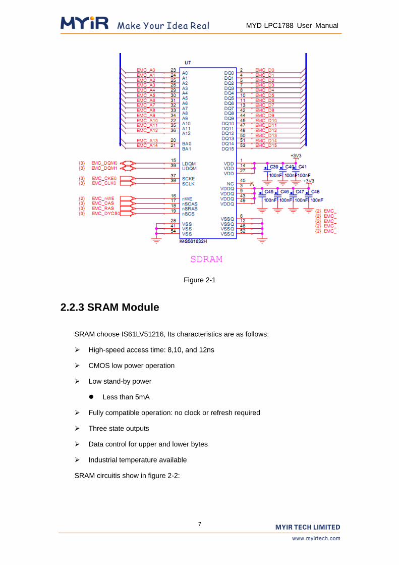
2.2.2 SDRAM Module
SDRAM chooses K4S561632H. Its characteristics are as follows:
Auto refresh
64ms refresh cycles
SDRAM circuit is shown in figure 2-1:
7
MYD-LPC1788 User Manual
Figure 2-1
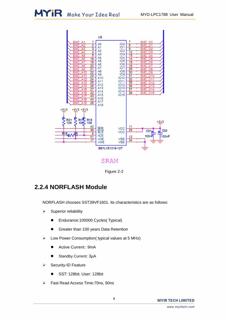
2.2.3 SRAM Module
SRAM choose IS61LV51216, Its characteristics are as follows:
High-speed access time: 8,10, and 12ns
CMOS low power operation
Low stand-by power
Less than 5mA
Fully compatible operation: no clock or refresh required
Three state outputs
Data control for upper and lower bytes
Industrial temperature available
SRAM circuitis show in figure 2-2:
8
MYD-LPC1788 User Manual
Figure 2-2
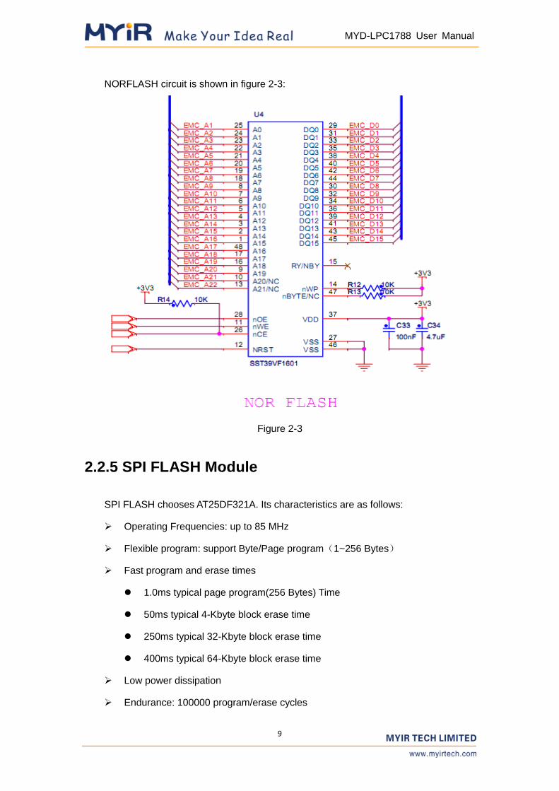
2.2.4 NORFLASH Module
NORFLASH chooses SST39VF1601. Its characteristics are as follows:
Superior reliability
Endurance:100000 Cycles( Typical)
Greater than 100 years Data Retention
Low Power Consumption( typical values at 5 MHz)
Active Current:: 9mA
Standby Current: 3µA
Security-ID Feature
SST: 128bit; User: 128bit
Fast Read Access Time:70ns, 90ns
9
MYD-LPC1788 User Manual
NORFLASH circuit is shown in figure 2-3:
Figure 2-3
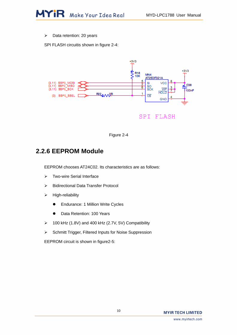
2.2.5 SPI FLASH Module
SPI FLASH chooses AT25DF321A. Its characteristics are as follows:
Operating Frequencies: up to 85 MHz
Flexible program: support Byte/Page program(1~256 Bytes)
Fast program and erase times
1.0ms typical page program(256 Bytes) Time
50ms typical 4-Kbyte block erase time
250ms typical 32-Kbyte block erase time
400ms typical 64-Kbyte block erase time
Low power dissipation
Endurance: 100000 program/erase cycles
10
MYD-LPC1788 User Manual
Data retention: 20 years
SPI FLASH circuitis shown in figure 2-4:
Figure 2-4
2.2.6 EEPROM Module
EEPROM chooses AT24C02. Its characteristics are as follows:
Two-wire Serial Interface
Bidirectional Data Transfer Protocol
High-reliability
Endurance: 1 Million Write Cycles
Data Retention: 100 Years
100 kHz (1.8V) and 400 kHz (2.7V, 5V) Compatibility
Schmitt Trigger, Filtered Inputs for Noise Suppression
EEPROM circuit is shown in figure2-5:
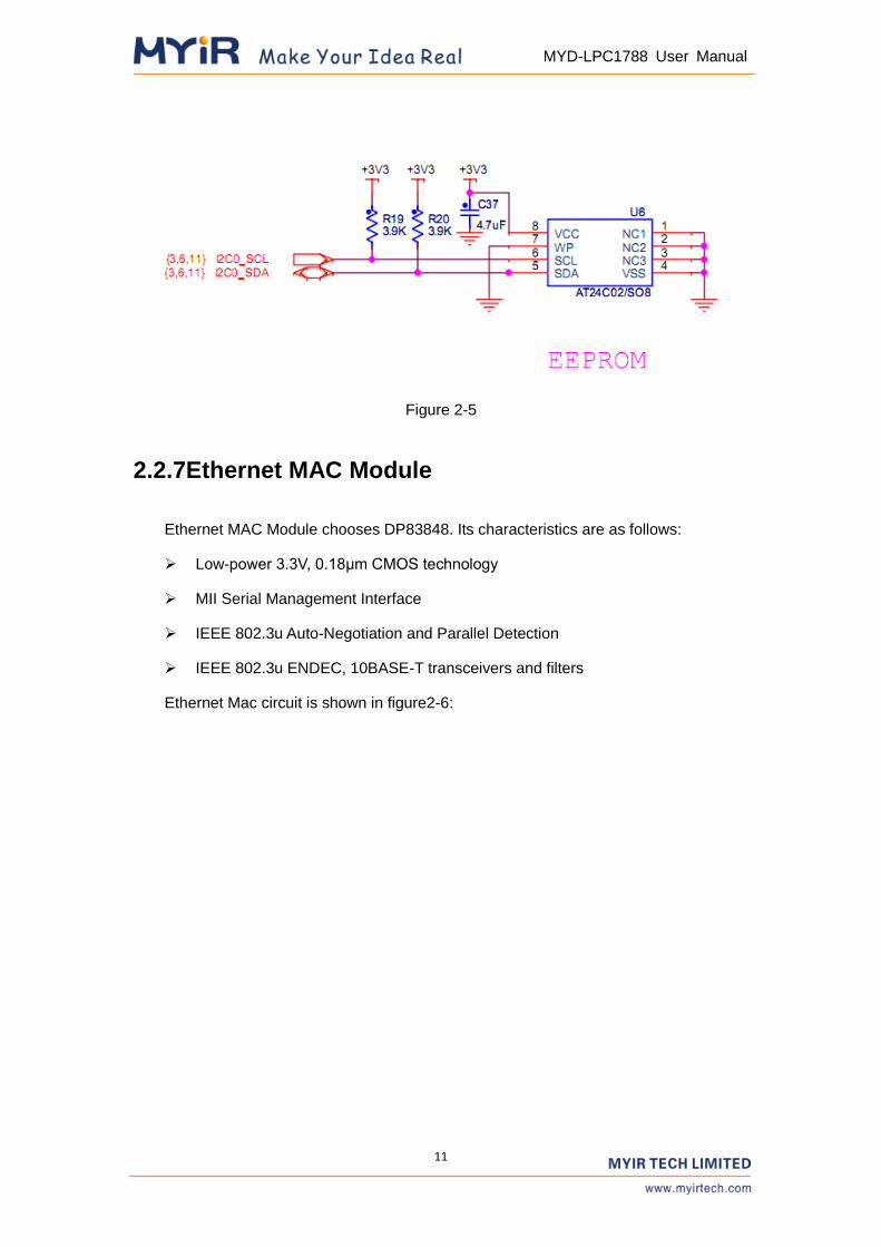
11
MYD-LPC1788 User Manual
Figure 2-5
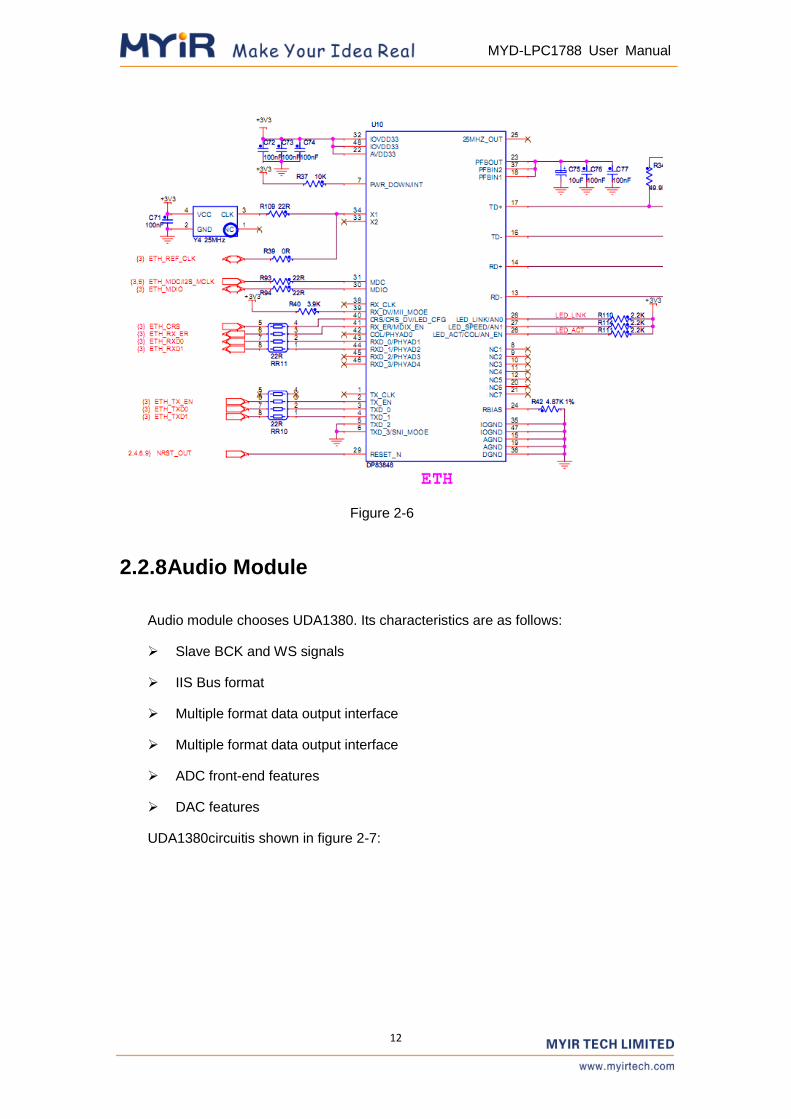
2.2.7Ethernet MAC Module
Ethernet MAC Module chooses DP83848. Its characteristics are as follows:
Low-power 3.3V, 0.18μm CMOS technology
MII Serial Management Interface
IEEE 802.3u Auto-Negotiation and Parallel Detection
IEEE 802.3u ENDEC, 10BASE-T transceivers and filters
Ethernet Mac circuit is shown in figure2-6:
12
MYD-LPC1788 User Manual
Figure 2-6
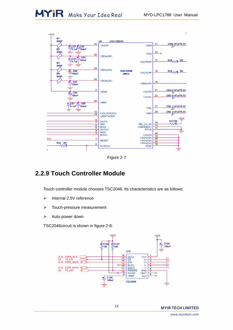
2.2.8Audio Module
Audio module chooses UDA1380. Its characteristics are as follows:
Slave BCK and WS signals
IIS Bus format
Multiple format data output interface
Multiple format data output interface
ADC front-end features
DAC features
UDA1380circuitis shown in figure 2-7:
13
MYD-LPC1788 User Manual
Figure 2-7
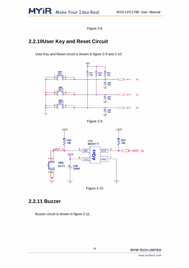
2.2.9 Touch Controller Module
Touch controller module chooses TSC2046. Its characteristics are as follows:
Internal 2.5V reference
Touch-pressure measurement
Auto power down
TSC2046circuit is shown in figure 2-8:
14
MYD-LPC1788 User Manual
Figure 2-8
2.2.10User Key and Reset Circuit
User Key and Reset circuit is shown in figure 2-9 and 2-10:
Figure 2-9
Figure 2-10
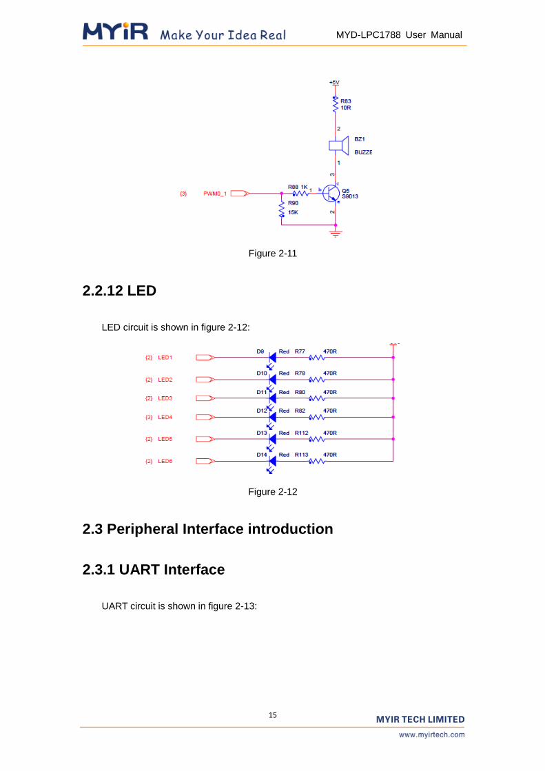
2.2.11 Buzzer
Buzzer circuit is shown in figure 2-11:
15
MYD-LPC1788 User Manual
Figure 2-11
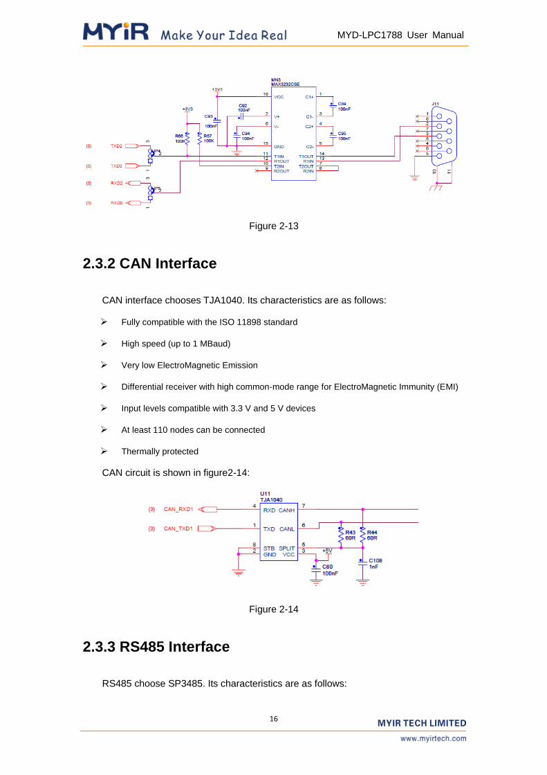
2.2.12 LED
LED circuit is shown in figure 2-12:
Figure 2-12
2.3 Peripheral Interface introduction
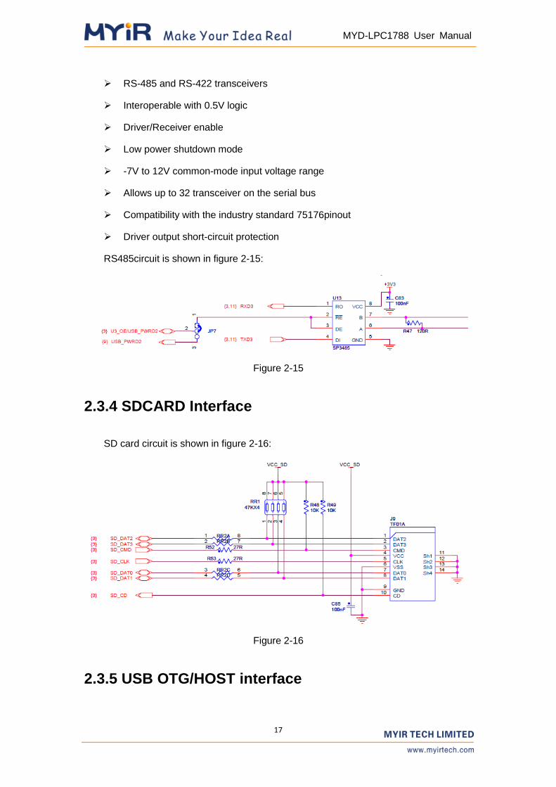
2.3.1 UART Interface
UART circuit is shown in figure 2-13:
16
MYD-LPC1788 User Manual
Figure 2-13
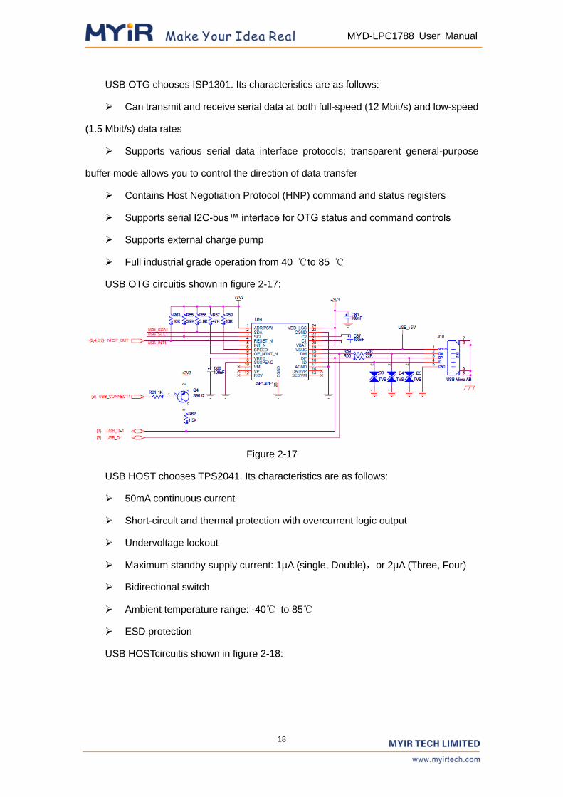
2.3.2 CAN Interface
CAN interface chooses TJA1040. Its characteristics are as follows:
Fully compatible with the ISO 11898 standard
High speed (up to 1 MBaud)
Very low ElectroMagnetic Emission
Differential receiver with high common-mode range for ElectroMagnetic Immunity (EMI)
Input levels compatible with 3.3 V and 5 V devices
At least 110 nodes can be connected
Thermally protected
CAN circuit is shown in figure2-14:
Figure 2-14
2.3.3 RS485 Interface
RS485 choose SP3485. Its characteristics are as follows:
17
MYD-LPC1788 User Manual
RS-485 and RS-422 transceivers
Interoperable with 0.5V logic
Driver/Receiver enable
Low power shutdown mode
-7V to 12V common-mode input voltage range
Allows up to 32 transceiver on the serial bus
Compatibility with the industry standard 75176pinout
Driver output short-circuit protection
RS485circuit is shown in figure 2-15:
Figure 2-15
2.3.4 SDCARD Interface
SD card circuit is shown in figure 2-16:
Figure 2-16
2.3.5 USB OTG/HOST interface
18
MYD-LPC1788 User Manual
USB OTG chooses ISP1301. Its characteristics are as follows:
Can transmit and receive serial data at both full-speed (12 Mbit/s) and low-speed
(1.5 Mbit/s) data rates
Supports various serial data interface protocols; transparent general-purpose
buffer mode allows you to control the direction of data transfer
Contains Host Negotiation Protocol (HNP) command and status registers
Supports serial I2C-bus™ interface for OTG status and command controls
Supports external charge pump
Full industrial grade operation from 40 ℃to 85 ℃
USB OTG circuitis shown in figure 2-17:
Figure 2-17
USB HOST chooses TPS2041. Its characteristics are as follows:
50mA continuous current
Short-circult and thermal protection with overcurrent logic output
Undervoltage lockout
Maximum standby supply current: 1µA (single, Double),or 2µA (Three, Four)
Bidirectional switch
Ambient temperature range: -40℃ to 85℃
ESD protection
USB HOSTcircuitis shown in figure 2-18:
19
MYD-LPC1788 User Manual
Figure 2-18
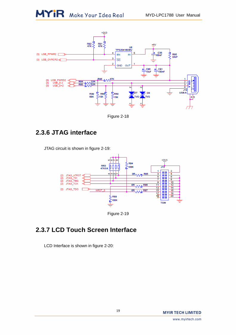
2.3.6 JTAG interface
JTAG circuit is shown in figure 2-19:
Figure 2-19
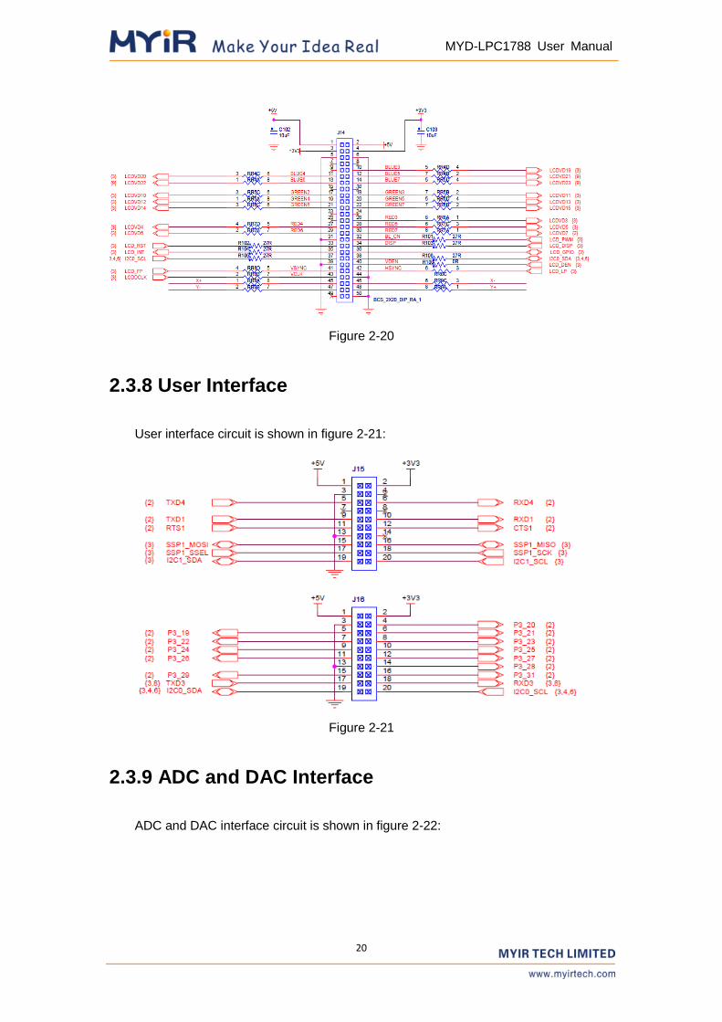
2.3.7 LCD Touch Screen Interface
LCD Interface is shown in figure 2-20:
20
MYD-LPC1788 User Manual
Figure 2-20
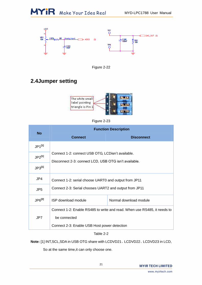
2.3.8 User Interface
User interface circuit is shown in figure 2-21:
Figure 2-21
2.3.9 ADC and DAC Interface
ADC and DAC interface circuit is shown in figure 2-22:
21
MYD-LPC1788 User Manual
Figure 2-22
2.4Jumper setting
Figure 2-23
No Function Description
Connect Disconnect
JP1[1]
Connect 1-2: connect USB OTG, LCDisn’t available.
Disconnect 2-3: connect LCD, USB OTG isn’t available. JP2
[1]
JP3[1]
JP4 Connect 1-2: serial choose UART0 and output from JP11
Connect 2-3: Serial chooses UART2 and output from JP11 JP5
JP6[2]
ISP download module Normal download module
JP7
Connect 1-2: Enable RS485 to write and read. When use RS485, it needs to
be connected
Connect 2-3: Enable USB Host power detection
Table 2-2
Note: [1] INT,SCL,SDA in USB OTG share with LCDVD21、LCDVD22、LCDVD23 in LCD,
So at the same time,it can only choose one.

22
MYD-LPC1788 User Manual
[2] Connect JP6 when download program in ISP module. After download program,
reset board, program start to run.
23
MYD-LPC1788 User Manual
Chapter 3 MDK Routine
3.1 Overview
MDK routines are naked programs without operating system and its development tool
is MDK-ARM 4.53. This chapter describes how to use and writetest procedures. The
contents include:
(1) MDK development environment to be built and configured;
(2) MDK sample program debugged, compiled and downloaded;
(3) The test procedures: functions, usage and phenomenon descriptions.
MDK routines cover a wide range of programs, including DMA, ADC, LCD, Memory,
Ethernet MAC and so on. User can make a second development on these examples,
which can shorten developmentcycle.
3.2 Preparation
(1) Install MDK-ARM (Version 4.53) development tool and license and then Prepare
for MYD-LPC1788 board.
(2) Set serial:Baud Rate: 115200; Data Bits: 8; Parity Bit: None; Stop Bit: 1. Data flow:
None.
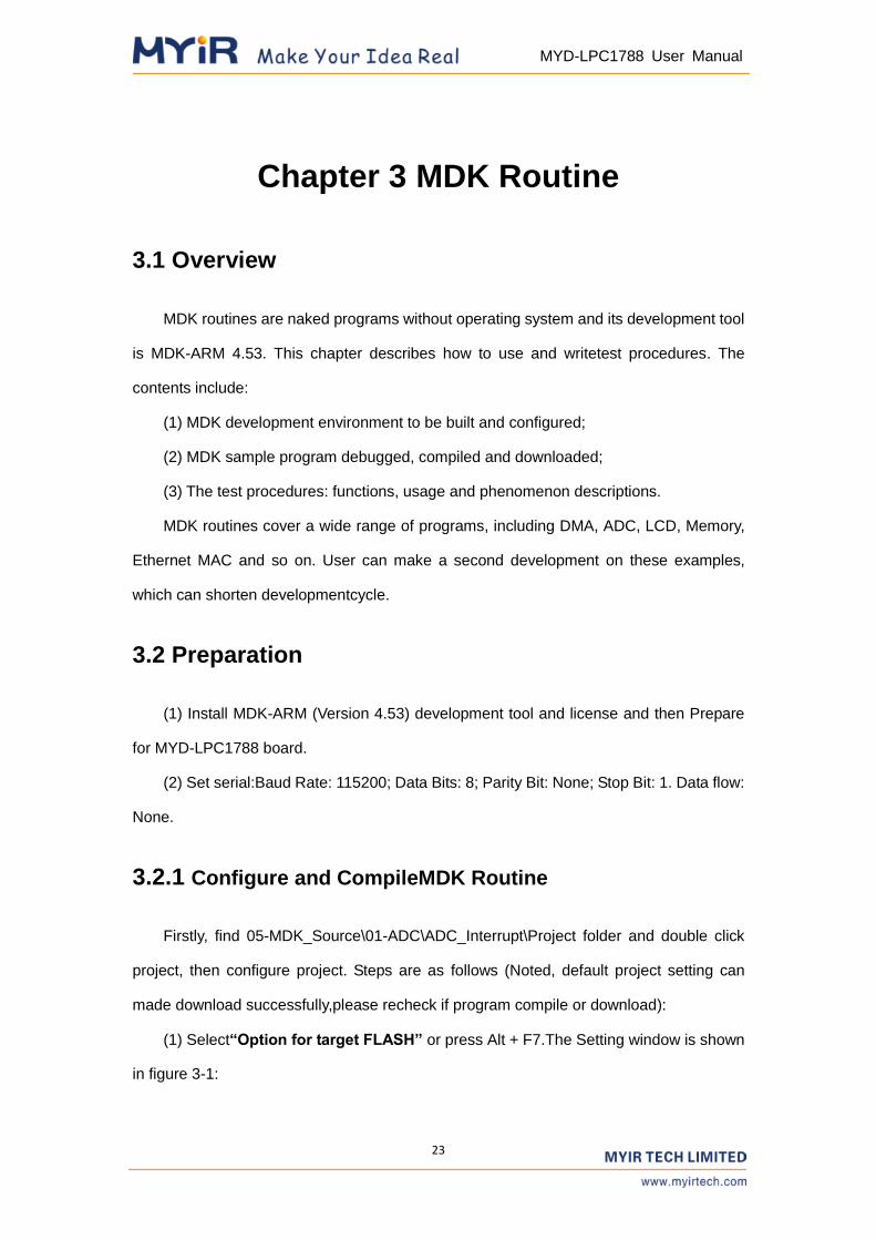
3.2.1 Configure and CompileMDK Routine
Firstly, find 05-MDK_Source\01-ADC\ADC_Interrupt\Project folder and double click
project, then configure project. Steps are as follows (Noted, default project setting can
made download successfully,please recheck if program compile or download):
(1) Select“Option for target FLASH” or press Alt + F7.The Setting window is shown
in figure 3-1:
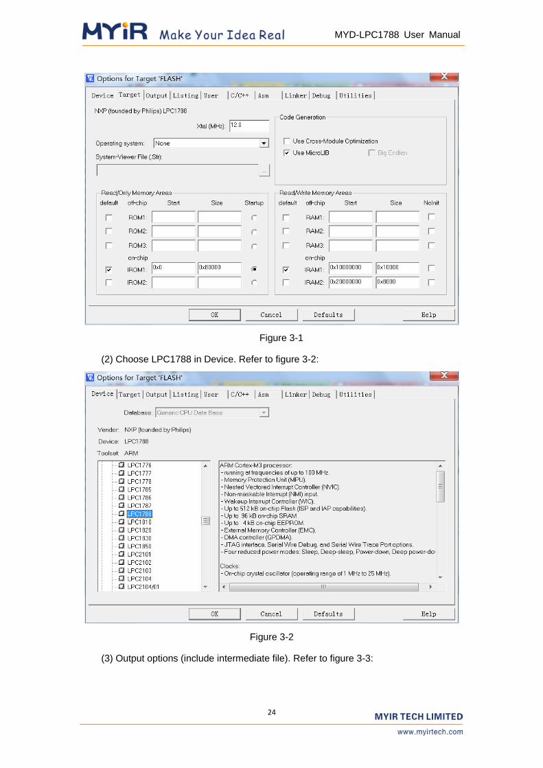
24
MYD-LPC1788 User Manual
Figure 3-1
(2) Choose LPC1788 in Device. Refer to figure 3-2:
Figure 3-2
(3) Output options (include intermediate file). Refer to figure 3-3:
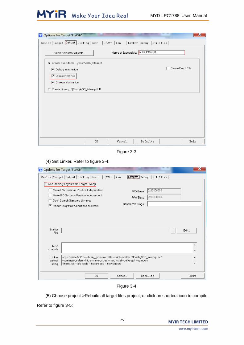
25
MYD-LPC1788 User Manual
Figure 3-3
(4) Set Linker. Refer to figure 3-4:
Figure 3-4
(5) Choose project->Rebuild all target files project, or click on shortcut icon to compile.
Refer to figure 3-5:
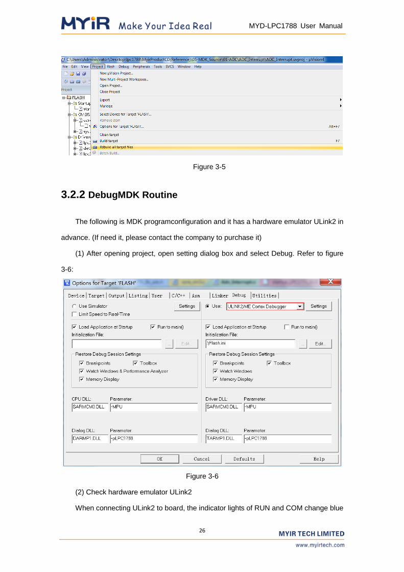
26
MYD-LPC1788 User Manual
Figure 3-5
3.2.2 DebugMDK Routine
The following is MDK programconfiguration and it has a hardware emulator ULink2 in
advance. (If need it, please contact the company to purchase it)
(1) After opening project, open setting dialog box and select Debug. Refer to figure
3-6:
Figure 3-6
(2) Check hardware emulator ULink2
When connecting ULink2 to board, the indicator lights of RUN and COM change blue
27
MYD-LPC1788 User Manual
and then turn off, while USB indicator lights change red and then remain the same. Thus,
it indicates ULink2 is no problem.
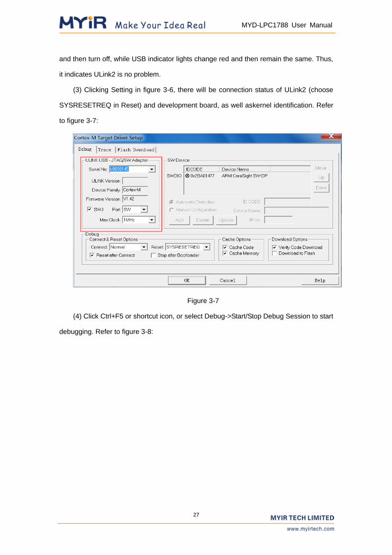
(3) Clicking Setting in figure 3-6, there will be connection status of ULink2 (choose
SYSRESETREQ in Reset) and development board, as well askernel identification. Refer
to figure 3-7:
Figure 3-7
(4) Click Ctrl+F5 or shortcut icon, or select Debug->Start/Stop Debug Session to start
debugging. Refer to figure 3-8:
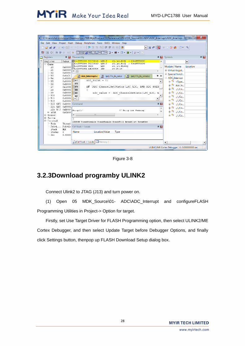
28
MYD-LPC1788 User Manual
Figure 3-8
3.2.3Download programby ULINK2
Connect Ulink2 to JTAG (J13) and turn power on.
(1) Open 05 MDK_Source\01- ADC\ADC_Interrupt and configureFLASH
Programming Utilities in Project-> Option for target.
Firstly, set Use Target Driver for FLASH Programming option, then select ULINK2/ME
Cortex Debugger, and then select Update Target before Debugger Options, and finally
click Settings button, thenpop up FLASH Download Setup dialog box.
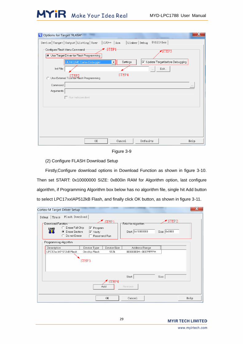
29
MYD-LPC1788 User Manual
Figure 3-9
(2) Configure FLASH Download Setup
Firstly,Configure download options in Download Function as shown in figure 3-10.
Then set START: 0x10000000 SIZE: 0x800in RAM for Algorithm option, last configure
algorithm, if Programming Algorithm box below has no algorithm file, single hit Add button
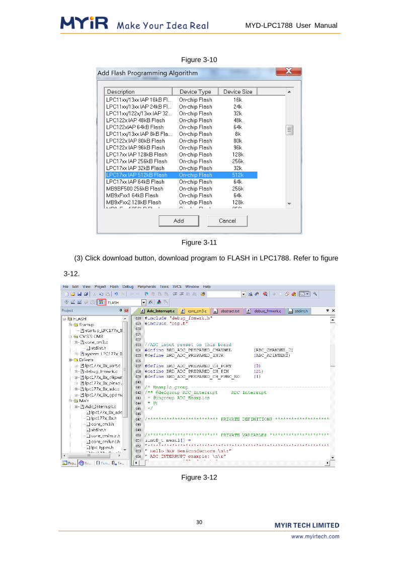
to select LPC17xxIAP512kB Flash, and finally click OK button, as shown in figure 3-11.
30
MYD-LPC1788 User Manual
Figure 3-10
Figure 3-11
(3) Click download button, download program to FLASH in LPC1788. Refer to figure
3-12.
Figure 3-12
31
MYD-LPC1788 User Manual
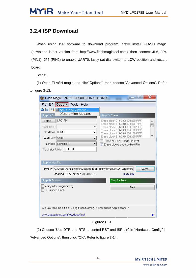
3.2.4 ISP Download
When using ISP software to download program, firstly install FLASH magic
(download latest version from http://www.flashmagictool.com), then connect JP6, JP4
(PIN1), JP5 (PIN2) to enable UART0, lastly set dial switch to LOW position and restart
board.
Steps:
(1) Open FLASH magic and click“Options”, then choose “Advanced Options”. Refer
to figure 3-13:
Figurec3-13
(2) Choose “Use DTR and RTS to control RST and ISP pin” in “Hardware Config” in
“Advanced Options”, then click “OK”. Refer to figure 3-14:
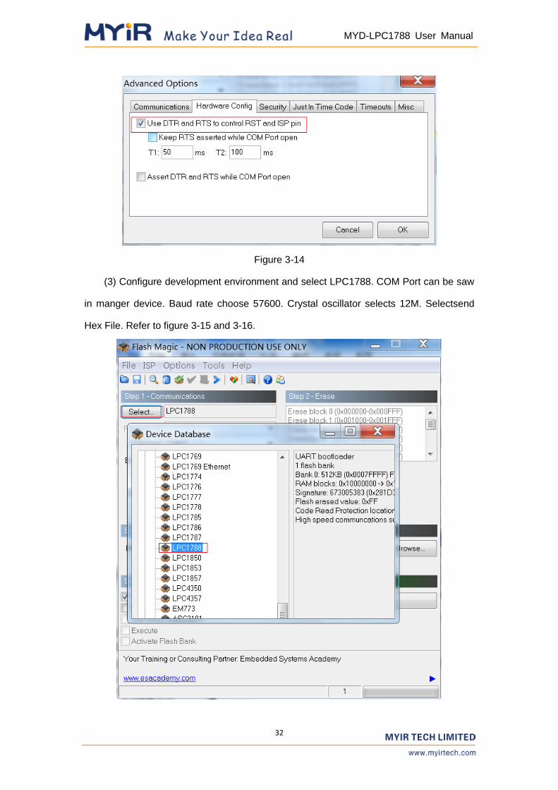
32
MYD-LPC1788 User Manual
Figure 3-14
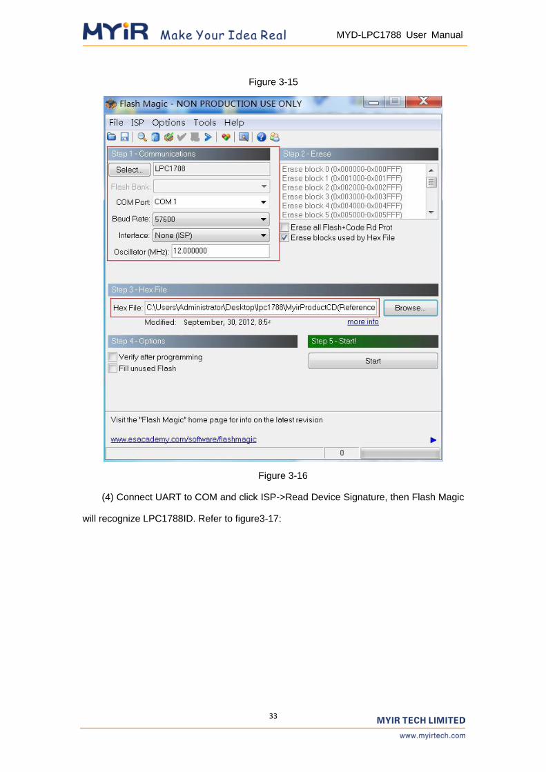
(3) Configure development environment and select LPC1788. COM Port can be saw
in manger device. Baud rate choose 57600. Crystal oscillator selects 12M. Selectsend
Hex File. Refer to figure 3-15 and 3-16.
33
MYD-LPC1788 User Manual
Figure 3-15
Figure 3-16
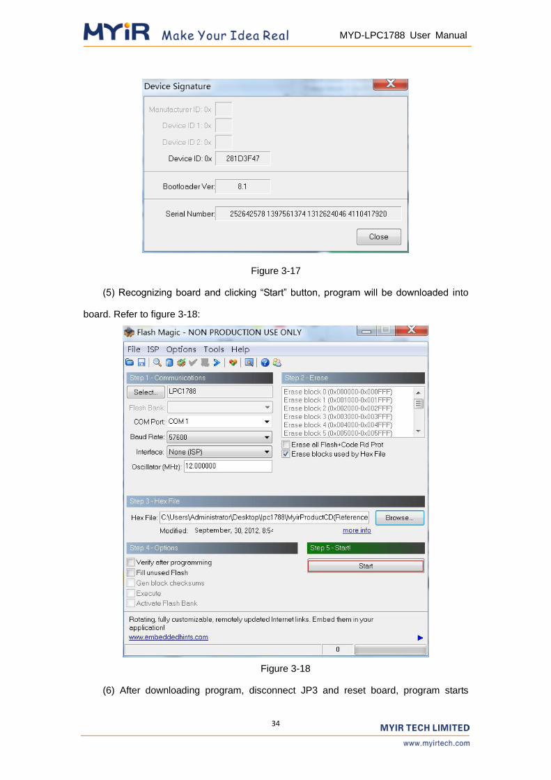
(4) Connect UART to COM and click ISP->Read Device Signature, then Flash Magic
will recognize LPC1788ID. Refer to figure3-17:
34
MYD-LPC1788 User Manual
Figure 3-17
(5) Recognizing board and clicking “Start” button, program will be downloaded into
board. Refer to figure 3-18:
Figure 3-18
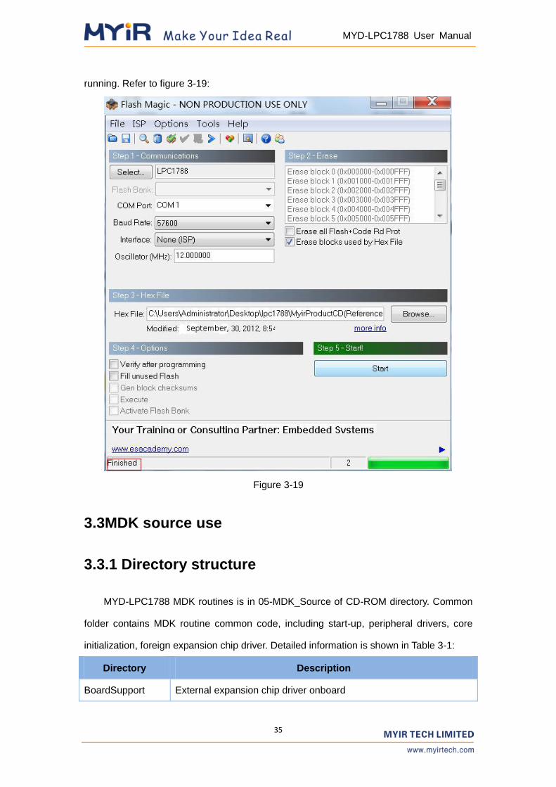
(6) After downloading program, disconnect JP3 and reset board, program starts
35
MYD-LPC1788 User Manual
running. Refer to figure 3-19:
Figure 3-19
3.3MDK source use
3.3.1 Directory structure
MYD-LPC1788 MDK routines is in 05-MDK_Source of CD-ROM directory. Common
folder contains MDK routine common code, including start-up, peripheral drivers, core
initialization, foreign expansion chip driver. Detailed information is shown in Table 3-1:
Directory Description
BoardSupport External expansion chip driver onboard
36
MYD-LPC1788 User Manual
CoreSupport Macro definition of kernel function
DeviceSupport Boot code and system initialization code
Drivers Peripheral drivers
Table 3-1
3.3.2 Add function module
When need to test or use a function module, add .C file in module and then contain
module header file in .C files, lastly call module function directly.
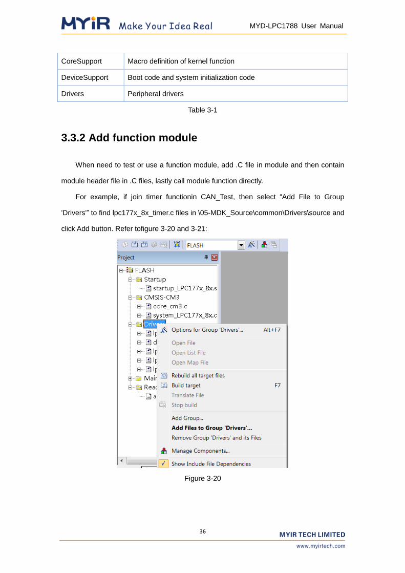
For example, if join timer functionin CAN_Test, then select “Add File to Group
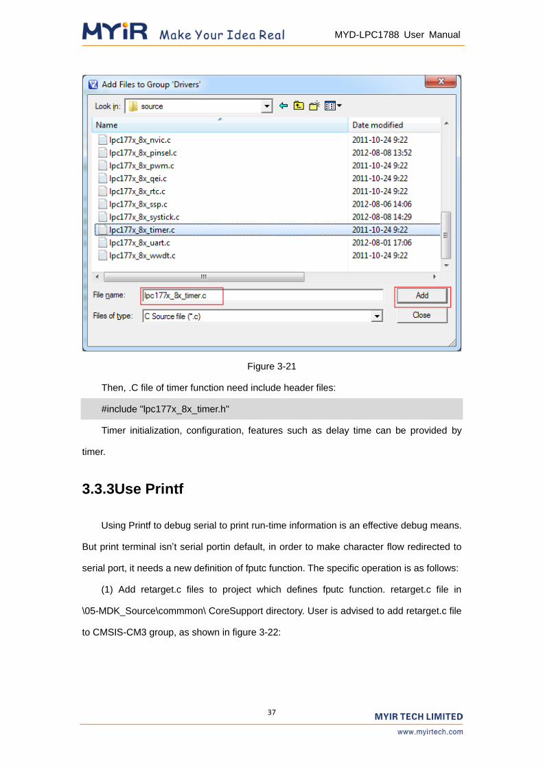
'Drivers'” to find lpc177x_8x_timer.c files in \05-MDK_Source\common\Drivers\source and
click Add button. Refer tofigure 3-20 and 3-21:
Figure 3-20
37
MYD-LPC1788 User Manual
Figure 3-21
Then, .C file of timer function need include header files:
#include "lpc177x_8x_timer.h"
Timer initialization, configuration, features such as delay time can be provided by
timer.
3.3.3Use Printf
Using Printf to debug serial to print run-time information is an effective debug means.
But print terminal isn’t serial portin default, in order to make character flow redirected to
serial port, it needs a new definition of fputc function. The specific operation is as follows:
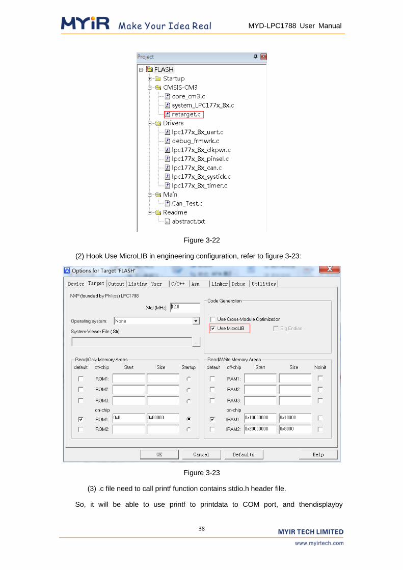
(1) Add retarget.c files to project which defines fputc function. retarget.c file in
\05-MDK_Source\commmon\ CoreSupport directory. User is advised to add retarget.c file
to CMSIS-CM3 group, as shown in figure 3-22:
38
MYD-LPC1788 User Manual
Figure 3-22
(2) Hook Use MicroLIB in engineering configuration, refer to figure 3-23:
Figure 3-23
(3) .c file need to call printf function contains stdio.h header file.
So, it will be able to use printf to printdata to COM port, and thendisplayby
39
MYD-LPC1788 User Manual
HyperTerminal.
3.4 The introduction of MDK routine
MDK routines use UART2 port to print debug information, so it needs to set JP4 and
JP5 to enable UART2 port (PIN2 connect PIN3 in JP4 and JP5 ), set baud rate: 115200, 8
data bits, one stop bits, no parity bit, no control flow.
Please note that after download, it needs to disconnect JP6 and then reset board in
ISP download, otherwise it may cause abnormal.
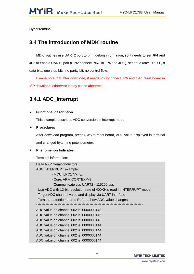
3.4.1 ADC_Interrupt
Functional description
This example describes ADC conversion in interrupt mode.
Procedures
After download program, press SW5 to reset board, ADC value displayed in terminal
and changed byturning potentiometer.
Phenomenon Indicates
Terminal information:
Hello NXP Semiconductors
ADC INTERRUPT example:
- MCU: LPC177x_8x
- Core: ARM CORTEX-M3
- Communicate via: UART2 - 115200 bps
Use ADC with 12-bit resolution rate of 400KHz, read in INTERRUPT mode
To get ADC channel value and display via UART interface
Turn the potentiometer to Refer to how ADC value changes
********************************************************************************
ADC value on channel 002 is: 0000000148
ADC value on channel 002 is: 0000000145
ADC value on channel 002 is: 0000000146
ADC value on channel 002 is: 0000000144
ADC value on channel 002 is: 0000000144
ADC value on channel 002 is: 0000000144
ADC value on channel 002 is: 0000000144
40
MYD-LPC1788 User Manual
ADC value on channel 002 is: 0000000146
ADC value on channel 002 is: 0000000146
ADC value on channel 002 is: 0000000146
ADC value on channel 002 is: 0000000144
ADC value on channel 002 is: 0000000144
ADC value on channel 002 is: 0000000146
ADC value on channel 002 is: 0000000146
ADC value on channel 002 is: 0000000144
ADC value on channel 002 is: 0000000146
ADC value on channel 002 is: 0000000146
ADC value on channel 002 is: 0000000146
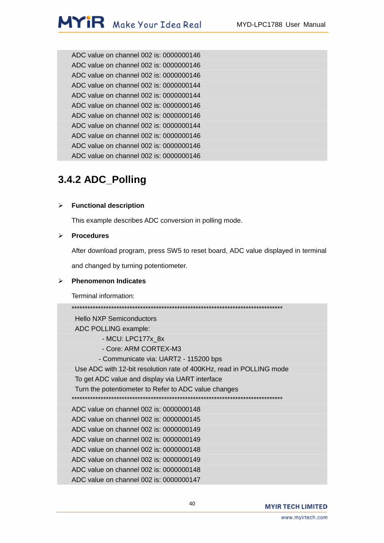
3.4.2 ADC_Polling
Functional description
This example describes ADC conversion in polling mode.
Procedures
After download program, press SW5 to reset board, ADC value displayed in terminal
and changed by turning potentiometer.
Phenomenon Indicates
Terminal information:
********************************************************************************
Hello NXP Semiconductors
ADC POLLING example:
- MCU: LPC177x_8x
- Core: ARM CORTEX-M3
- Communicate via: UART2 - 115200 bps
Use ADC with 12-bit resolution rate of 400KHz, read in POLLING mode
To get ADC value and display via UART interface
Turn the potentiometer to Refer to ADC value changes
********************************************************************************
ADC value on channel 002 is: 0000000148
ADC value on channel 002 is: 0000000145
ADC value on channel 002 is: 0000000149
ADC value on channel 002 is: 0000000149
ADC value on channel 002 is: 0000000148
ADC value on channel 002 is: 0000000149
ADC value on channel 002 is: 0000000148
ADC value on channel 002 is: 0000000147
41
MYD-LPC1788 User Manual
ADC value on channel 002 is: 0000000148
ADC value on channel 002 is: 0000000148
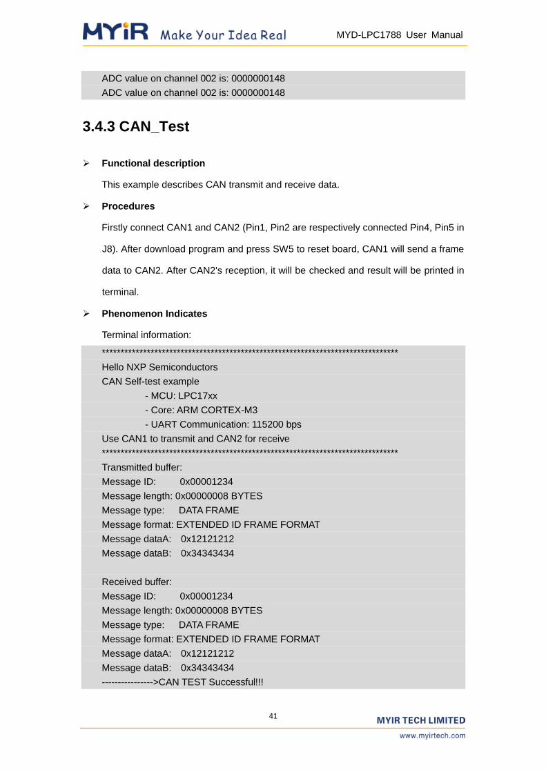
3.4.3 CAN_Test
Functional description
This example describes CAN transmit and receive data.
Procedures
Firstly connect CAN1 and CAN2 (Pin1, Pin2 are respectively connected Pin4, Pin5 in
J8). After download program and press SW5 to reset board, CAN1 will send a frame
data to CAN2. After CAN2's reception, it will be checked and result will be printed in
terminal.
Phenomenon Indicates
Terminal information:
*******************************************************************************
Hello NXP Semiconductors
CAN Self-test example
- MCU: LPC17xx
- Core: ARM CORTEX-M3
- UART Communication: 115200 bps
Use CAN1 to transmit and CAN2 for receive
*******************************************************************************
Transmitted buffer:
Message ID: 0x00001234
Message length: 0x00000008 BYTES
Message type: DATA FRAME
Message format: EXTENDED ID FRAME FORMAT
Message dataA: 0x12121212
Message dataB: 0x34343434
Received buffer:
Message ID: 0x00001234
Message length: 0x00000008 BYTES
Message type: DATA FRAME
Message format: EXTENDED ID FRAME FORMAT
Message dataA: 0x12121212
Message dataB: 0x34343434
---------------->CAN TEST Successful!!!
42
MYD-LPC1788 User Manual
3.4.4 Crc_Demo
Functional description
This example describes CRC engine.
Procedures
After download program, press SW5 to reset board.Program calculates CRC block
data firstly anddisplaycalculates result afterreceiving input.
Phenomenon Indicates
Terminal information:
********************************************************************************
Hello NXP Semiconductors
CRC Demo example:
- MCU: LPC177x_8x
- Core: ARM CORTEX-M3
- UART Communication: 115200 bps
Use CRC engine on LPC177x_8x to calculate CRC for a 8-bit block data
You can choose one of three polynomial type:
- CRC-CCITT
- CRC-16
- CRC-32
********************************************************************************
Block data:
0x00000000 0x00000001 0x00000002 0x00000003 0x00000004
0x00000005 0x00000006 0x00000007 0x00000008 0x00000009
0x0000000A 0x0000000B 0x0000000C 0x0000000D 0x0000000E
0x0000000F 0x00000010 0x00000011 0x00000012 0x00000013
0x00000014 0x00000015 0x00000016 0x00000017 0x00000018
0x00000019 0x0000001A 0x0000001B 0x0000001C 0x0000001D
0x0000001E 0x0000001F 0x00000020 0x00000021 0x00000022
0x00000023 0x00000024 0x00000025 0x00000026 0x00000027
0x00000028 0x00000029 0x0000002A 0x0000002B 0x0000002C
0x0000002D 0x0000002E 0x0000002F 0x00000030 0x00000031
0x00000032 0x00000033 0x00000034 0x00000035 0x00000036
0x00000037 0x00000038 0x00000039 0x0000003A 0x0000003B
0x0000003C 0x0000003D 0x0000003E 0x0000003F
Choose what polynomial that you want to use, type:
- '1': CRC-CCITT
- '2': CRC-16
- '3': CRC-32
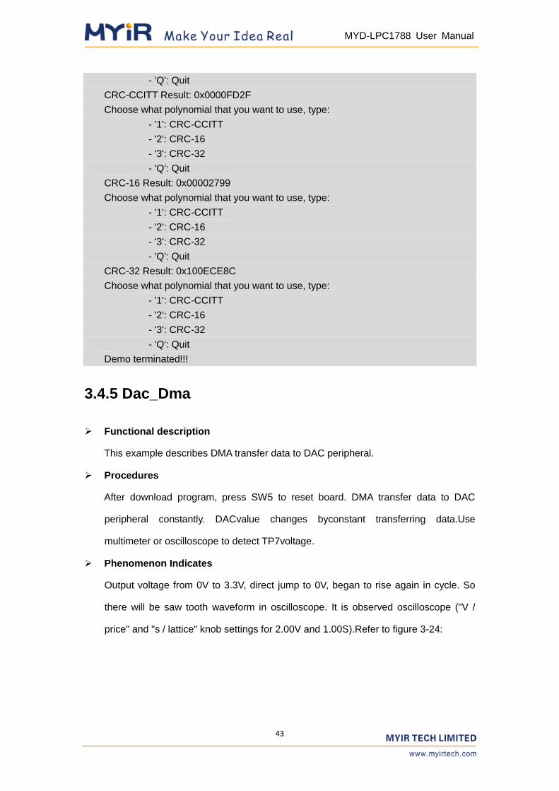
43
MYD-LPC1788 User Manual
- 'Q': Quit
CRC-CCITT Result: 0x0000FD2F
Choose what polynomial that you want to use, type:
- '1': CRC-CCITT
- '2': CRC-16
- '3': CRC-32
- 'Q': Quit
CRC-16 Result: 0x00002799
Choose what polynomial that you want to use, type:
- '1': CRC-CCITT
- '2': CRC-16
- '3': CRC-32
- 'Q': Quit
CRC-32 Result: 0x100ECE8C
Choose what polynomial that you want to use, type:
- '1': CRC-CCITT
- '2': CRC-16
- '3': CRC-32
- 'Q': Quit
Demo terminated!!!
3.4.5 Dac_Dma
Functional description
This example describes DMA transfer data to DAC peripheral.
Procedures
After download program, press SW5 to reset board. DMA transfer data to DAC
peripheral constantly. DACvalue changes byconstant transferring data.Use
multimeter or oscilloscope to detect TP7voltage.
Phenomenon Indicates
Output voltage from 0V to 3.3V, direct jump to 0V, began to rise again in cycle. So
there will be saw tooth waveform in oscilloscope. It is observed oscilloscope ("V /
price" and "s / lattice" knob settings for 2.00V and 1.00S).Refer to figure 3-24:
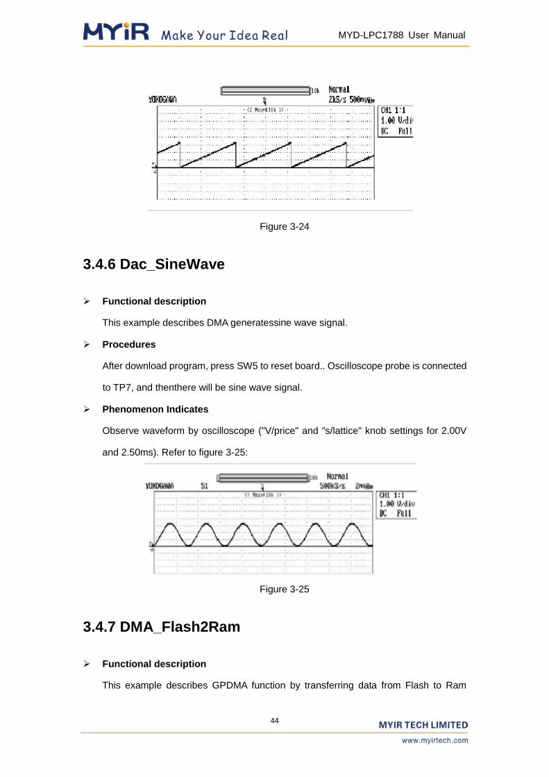
44
MYD-LPC1788 User Manual
Figure 3-24
3.4.6 Dac_SineWave
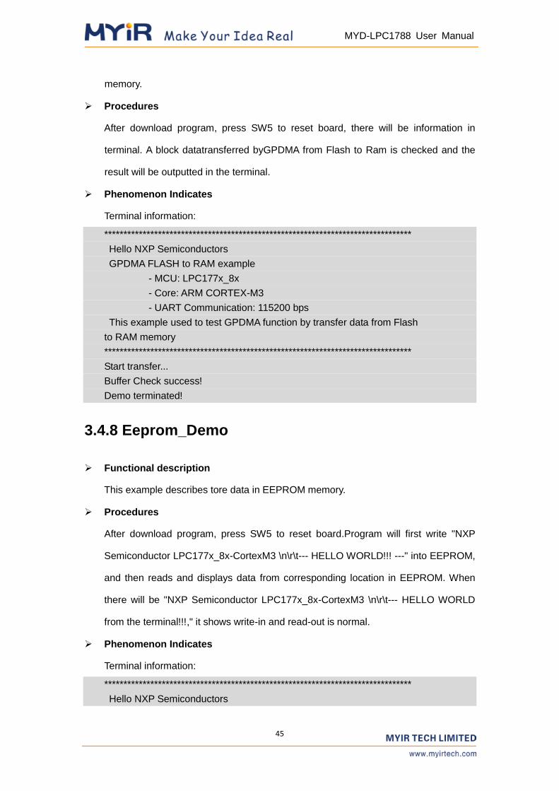
Functional description
This example describes DMA generatessine wave signal.
Procedures
After download program, press SW5 to reset board.. Oscilloscope probe is connected
to TP7, and thenthere will be sine wave signal.
Phenomenon Indicates
Observe waveform by oscilloscope ("V/price" and "s/lattice" knob settings for 2.00V
and 2.50ms). Refer to figure 3-25:
Figure 3-25
3.4.7 DMA_Flash2Ram
Functional description
This example describes GPDMA function by transferring data from Flash to Ram
45
MYD-LPC1788 User Manual
memory.
Procedures
After download program, press SW5 to reset board, there will be information in
terminal. A block datatransferred byGPDMA from Flash to Ram is checked and the
result will be outputted in the terminal.
Phenomenon Indicates
Terminal information:
********************************************************************************
Hello NXP Semiconductors
GPDMA FLASH to RAM example
- MCU: LPC177x_8x
- Core: ARM CORTEX-M3
- UART Communication: 115200 bps
This example used to test GPDMA function by transfer data from Flash
to RAM memory
********************************************************************************
Start transfer...
Buffer Check success!
Demo terminated!
3.4.8 Eeprom_Demo
Functional description
This example describes tore data in EEPROM memory.
Procedures
After download program, press SW5 to reset board.Program will first write "NXP
Semiconductor LPC177x_8x-CortexM3 \n\r\t--- HELLO WORLD!!! ---" into EEPROM,
and then reads and displays data from corresponding location in EEPROM. When
there will be "NXP Semiconductor LPC177x_8x-CortexM3 \n\r\t--- HELLO WORLD
from the terminal!!!," it shows write-in and read-out is normal.
Phenomenon Indicates
Terminal information:
********************************************************************************
Hello NXP Semiconductors
46
MYD-LPC1788 User Manual
EEPROM demo example
- MCU: LPC177x_8x
- Core: ARM CORTEX-M3
- Communicate via: UART2 - 115200 bps
This example used to demo EEPROM operation on LPC177x_8x.
A 'Hello' sentence will be written into EEPROM memory, then read back and check.
********************************************************************************
Write data to EEPROM
Read data from EEPROM
NXP Semiconductor LPC177x_8x-CortexM3
--- HELLO WORLD!!!---
Demo is terminated
3.4.9 Emc_NorFlashDemo
Functional description
This example describesEMC read/write NOR FLASH.
Procedures
After download program, press SW5 to reset board. Program firstly check
Manufacturer ID and Device ID of NorFlash chip(Model:SST39VF1601). Then entire
Flash memory will be erased. 2K block data will be written and read back for verify.
Phenomenon Indicates
Terminal information:
********************************************************************************
Hello NXP Semiconductors
EMC NORFLASH example
- MCU: LPC177x_8x
- Core: Cortex-M3
- UART Comunication: 115200 bps
Write and verify data with on-board NOR FLASH
********************************************************************************
Init NOR Flash...
Read NOR Flash ID...
Erase entire NOR Flash...
Write a block of 2K data to NOR Flash...
Verify data...
Verifying complete! Testing terminated!
47
MYD-LPC1788 User Manual
3.4.10 Emc_SdramDemo
Functional description
This example describes EMC read/write SDRAM.
Procedures
After download program, press SW5 to reset board. The process of program: clear
SDRAM and write data into SDRAM in 8-bits mode and verify in 32-bits read mode.
Then clear SDRAM and write data into SDRAM in 16-bits mode and verify in32-bits
read mode.
Phenomenon Indicates
Terminal information:
********************************************************************************
Hello NXP Semiconductors
Test SDRAM K4S561632J with LPC1788 EMC
- MCU: LPC177x_8x
- Core: Cortex-M3
- UART Comunication: 115200 kbps
Write and verify data with on-board SDRAM
********************************************************************************
Clear content of SDRAM...
Writing in 8 bits format...
Verifying data...
Continue writing in 16 bits format...
Clear content of SRAM...
Writing in 16 bits format...
Verifying complete, testing terminated!
3.4.11 Emc_SramDemo
Functional description
This example describes EMC read/write SRAM.
Procedures
After download program, press SW5 to reset board.After clear data and write data
into SRAM,program displays memory address.
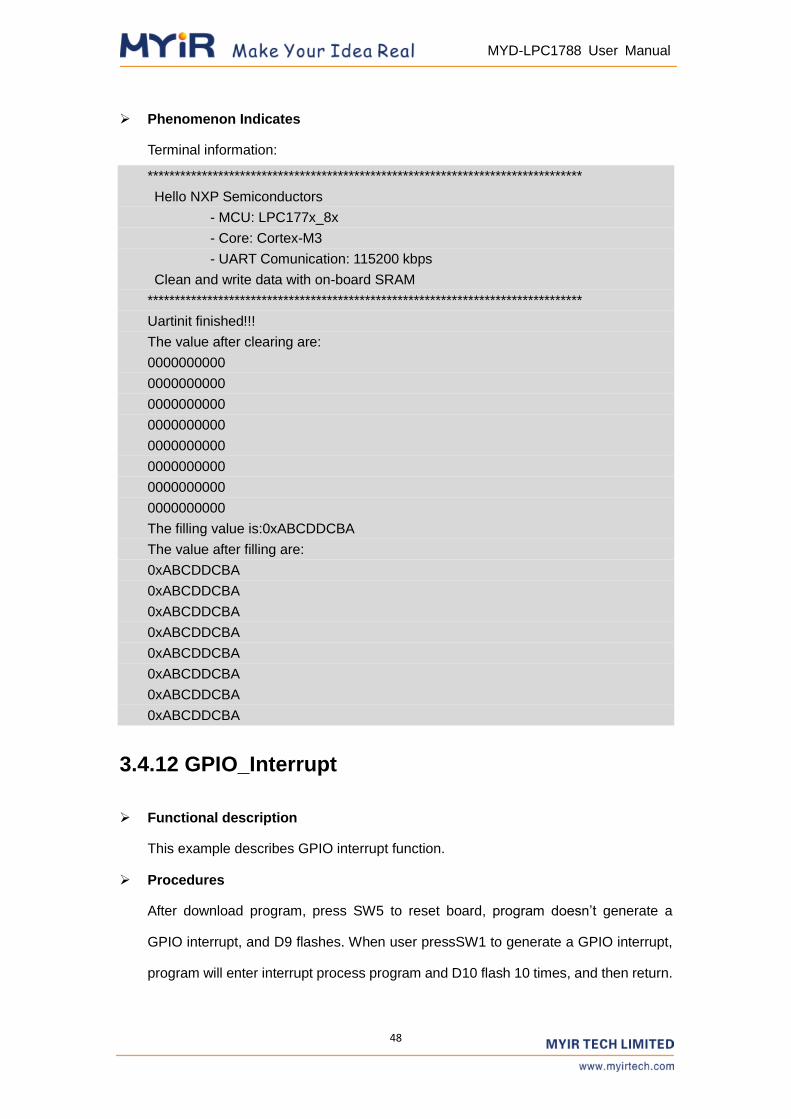
48
MYD-LPC1788 User Manual
Phenomenon Indicates
Terminal information:
********************************************************************************
Hello NXP Semiconductors
- MCU: LPC177x_8x
- Core: Cortex-M3
- UART Comunication: 115200 kbps
Clean and write data with on-board SRAM
********************************************************************************
Uartinit finished!!!
The value after clearing are:
0000000000
0000000000
0000000000
0000000000
0000000000
0000000000
0000000000
0000000000
The filling value is:0xABCDDCBA
The value after filling are:
0xABCDDCBA
0xABCDDCBA
0xABCDDCBA
0xABCDDCBA
0xABCDDCBA
0xABCDDCBA
0xABCDDCBA
0xABCDDCBA
3.4.12 GPIO_Interrupt
Functional description
This example describes GPIO interrupt function.
Procedures
After download program, press SW5 to reset board, program doesn’t generate a
GPIO interrupt, and D9 flashes. When user pressSW1 to generate a GPIO interrupt,
program will enter interrupt process program and D10 flash 10 times, and then return.
49
MYD-LPC1788 User Manual
Phenomenon Indicates
When program doesn’t generate a GPIO interrupt, D10 light and D9 flash. When
press SW1, D9 keep origin status and D10 flashes.
3.4.13 GPIO_LedBlinky
Functional description
This program describes GPIO drives LED.
Procedures
After download program, press SW5 to reset board, D9 flashes.
Phenomenon Indicates
Reset board, andD9 flashes.
3.4.14 Nvic_VectorTableRelocation
Functional description
This example describes relocation vector table.
Procedures
After download program, press SW5 to reset board.Vector Table will be remapped at
new address 0x20001000. If remapping is successful, SysTick interrupt can driver D9
flash normally.
Phenomenon Indicates
Terminal information:
********************************************************************************
Hello NXP Semiconductors
Privileged demo
- MCU: LPC177x_8x
- Core: ARM CORTEX-M3
- UART Communication: 115200 bps
This example used to test NVIC Vector Table Relocation function
********************************************************************************
Remapping Vector Table at address: 0x20001000
If Vector Table remapping is successful, LED D9 will blink by using
50
MYD-LPC1788 User Manual
SysTick interrupt
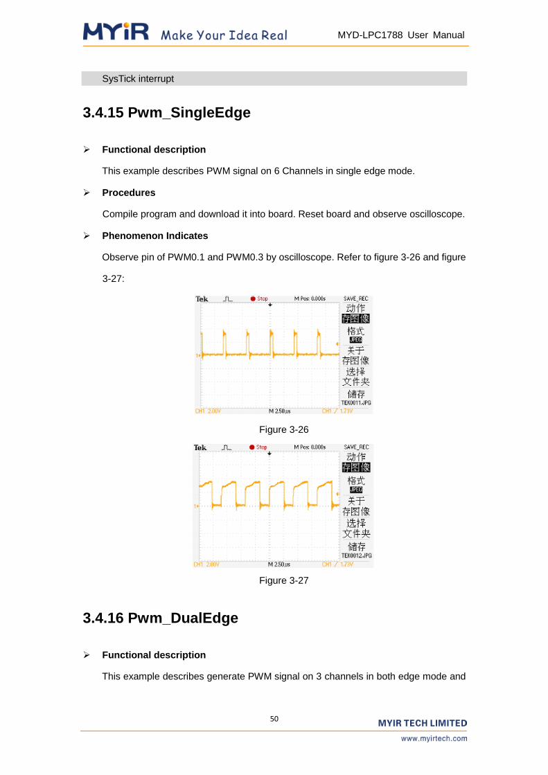
3.4.15 Pwm_SingleEdge
Functional description
This example describes PWM signal on 6 Channels in single edge mode.
Procedures
Compile program and download it into board. Reset board and observe oscilloscope.
Phenomenon Indicates
Observe pin of PWM0.1 and PWM0.3 by oscilloscope. Refer to figure 3-26 and figure
3-27:
Figure 3-26
Figure 3-27
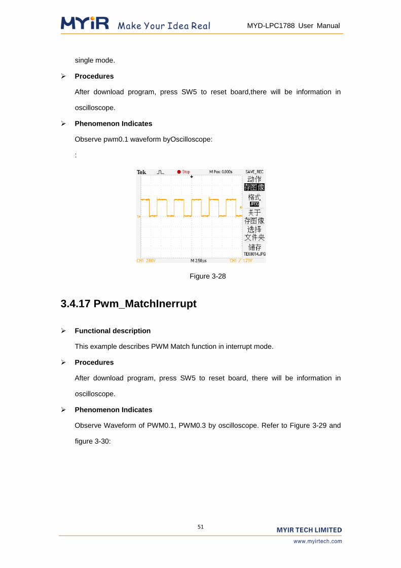
3.4.16 Pwm_DualEdge
Functional description
This example describes generate PWM signal on 3 channels in both edge mode and
51
MYD-LPC1788 User Manual
single mode.
Procedures
After download program, press SW5 to reset board,there will be information in
oscilloscope.
Phenomenon Indicates
Observe pwm0.1 waveform byOscilloscope:
:
Figure 3-28
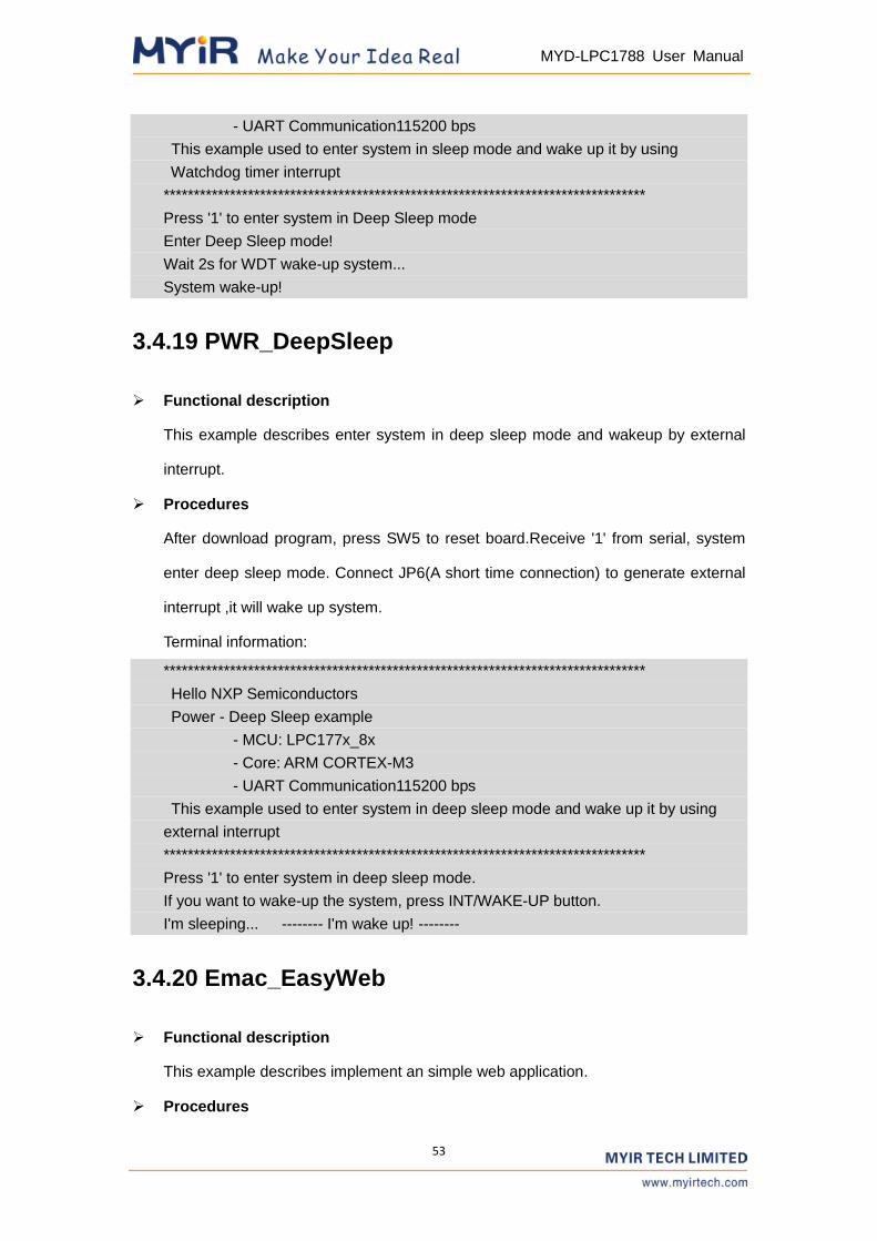
3.4.17 Pwm_MatchInerrupt
Functional description
This example describes PWM Match function in interrupt mode.
Procedures
After download program, press SW5 to reset board, there will be information in
oscilloscope.
Phenomenon Indicates
Observe Waveform of PWM0.1, PWM0.3 by oscilloscope. Refer to Figure 3-29 and
figure 3-30:
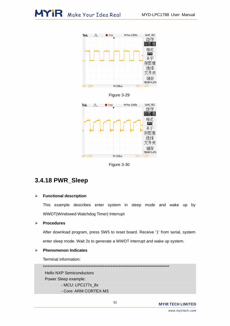
52
MYD-LPC1788 User Manual
Figure 3-29
Figure 3-30
3.4.18 PWR_Sleep
Functional description
This example describes enter system in sleep mode and wake up by
WWDT(Windowed Watchdog Timer) Interrupt
Procedures
After download program, press SW5 to reset board. Receive '1' from serial, system
enter sleep mode. Wait 2s to generate a WWDT interrupt and wake up system.
Phenomenon Indicates
Terminal information:
********************************************************************************
Hello NXP Semiconductors
Power Sleep example:
- MCU: LPC177x_8x
- Core: ARM CORTEX-M3
53
MYD-LPC1788 User Manual
- UART Communication115200 bps
This example used to enter system in sleep mode and wake up it by using
Watchdog timer interrupt
********************************************************************************
Press '1' to enter system in Deep Sleep mode
Enter Deep Sleep mode!
Wait 2s for WDT wake-up system...
System wake-up!
3.4.19 PWR_DeepSleep
Functional description
This example describes enter system in deep sleep mode and wakeup by external
interrupt.
Procedures
After download program, press SW5 to reset board.Receive '1' from serial, system
enter deep sleep mode. Connect JP6(A short time connection) to generate external
interrupt ,it will wake up system.
Terminal information:
********************************************************************************
Hello NXP Semiconductors
Power - Deep Sleep example
- MCU: LPC177x_8x
- Core: ARM CORTEX-M3
- UART Communication115200 bps
This example used to enter system in deep sleep mode and wake up it by using
external interrupt
********************************************************************************
Press '1' to enter system in deep sleep mode.
If you want to wake-up the system, press INT/WAKE-UP button.
I'm sleeping... -------- I'm wake up! --------
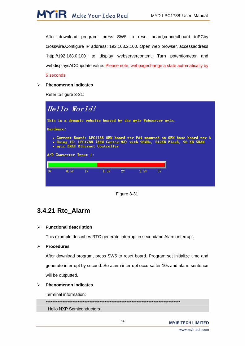
3.4.20 Emac_EasyWeb
Functional description
This example describes implement an simple web application.
Procedures
54
MYD-LPC1788 User Manual
After download program, press SW5 to reset board,connectboard toPCby
crosswire.Configure IP address: 192.168.2.100. Open web browser, accessaddress
"http://192.168.0.100" to display webservercontent. Turn potentiometer and
webdisplaysADCupdate value. Please note, webpagechange a state automatically by
5 seconds.
Phenomenon Indicates
Refer to figure 3-31:
Figure 3-31
3.4.21 Rtc_Alarm
Functional description
This example describes RTC generate interrupt in secondand Alarm interrupt.
Procedures
After download program, press SW5 to reset board. Program set initialize time and
generate interrupt by second. So alarm interrupt occursafter 10s and alarm sentence
will be outputted.
Phenomenon Indicates
Terminal information:
********************************************************************************
Hello NXP Semiconductors
55
MYD-LPC1788 User Manual
RTC Alarm Example:
- MCU: LPC177x_8x
- Core: ARM CORTEX-M3
- UART Communication: 115200 bps
A simple RTC example.
To generate interrupt in Second Counter Increment Interrupt (1s)
and generate Alarm interrupt at 10s
********************************************************************************
Current time set to: 018:045:000 025/003/02011
Second ALARM set to 010s
Second: 001
Second: 002
Second: 003
Second: 004
Second: 005
Second: 006
Second: 007
Second: 008
Second: 009
Second: 010
ALARM 10s matched!
Second: 011
Second: 012
Second: 013
Second: 014
Second: 015
3.4.22 SSP_Touchscreen
Functional description
The program shows SSP interface read position x and y in touchscreen.
Procedures
After download program, press SW5 to reset board, here will becurrent position X and
Y in terminal.
Phenomenon Indicates
Terminal information:
********************************************************************************
Hello NXP Semiconductors
SSP Touchscreen Example:
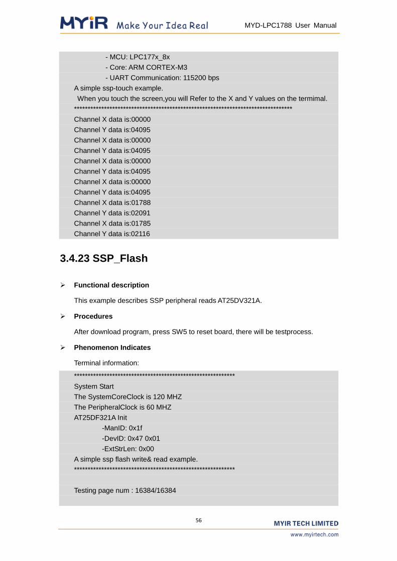
56
MYD-LPC1788 User Manual
- MCU: LPC177x_8x
- Core: ARM CORTEX-M3
- UART Communication: 115200 bps
A simple ssp-touch example.
When you touch the screen,you will Refer to the X and Y values on the termimal.
********************************************************************************
Channel X data is:00000
Channel Y data is:04095
Channel X data is:00000
Channel Y data is:04095
Channel X data is:00000
Channel Y data is:04095
Channel X data is:00000
Channel Y data is:04095
Channel X data is:01788
Channel Y data is:02091
Channel X data is:01785
Channel Y data is:02116
3.4.23 SSP_Flash
Functional description
This example describes SSP peripheral reads AT25DV321A.
Procedures
After download program, press SW5 to reset board, there will be testprocess.
Phenomenon Indicates
Terminal information:
***********************************************************
System Start
The SystemCoreClock is 120 MHZ
The PeripheralClock is 60 MHZ
AT25DF321A Init
-ManID: 0x1f
-DevID: 0x47 0x01
-ExtStrLen: 0x00
A simple ssp flash write& read example.
***********************************************************
Testing page num : 16384/16384
57
MYD-LPC1788 User Manual
############# Test finish. Error bytes: 0 #############
3.4.24 Systick_100msBase
Functional description
This example describes configure System Tick timer to generate interrupt each
100ms.
Procedures
AAfter download program, press SW5 to reset board. The program configures system
tick to generate interrupt at each 100ms. Generating interrupt changesD9status each
time.
Phenomenon Indicates
D9 flash is at 5Hz.
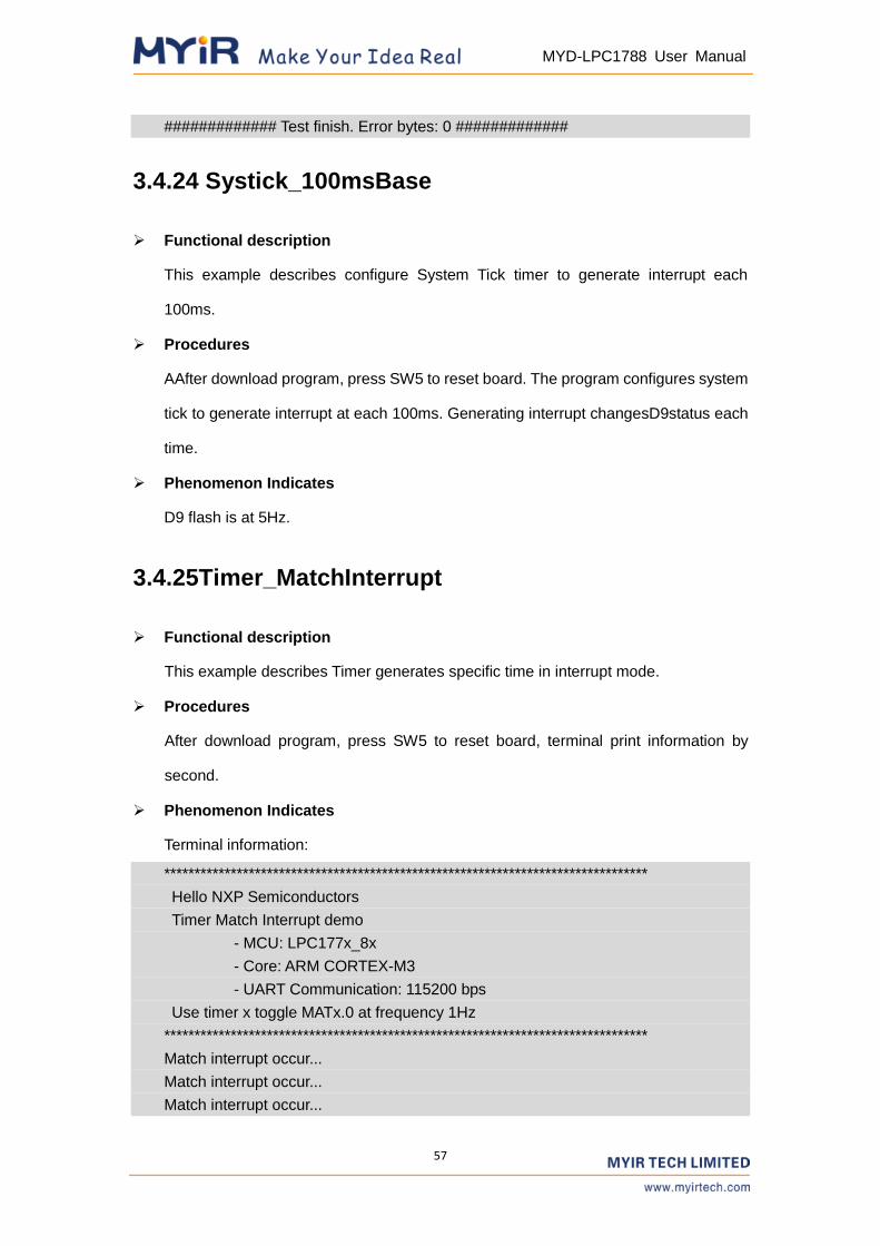
3.4.25Timer_MatchInterrupt
Functional description
This example describes Timer generates specific time in interrupt mode.
Procedures
After download program, press SW5 to reset board, terminal print information by
second.
Phenomenon Indicates
Terminal information:
********************************************************************************
Hello NXP Semiconductors
Timer Match Interrupt demo
- MCU: LPC177x_8x
- Core: ARM CORTEX-M3
- UART Communication: 115200 bps
Use timer x toggle MATx.0 at frequency 1Hz
********************************************************************************
Match interrupt occur...
Match interrupt occur...
Match interrupt occur...
58
MYD-LPC1788 User Manual
Match interrupt occur...
Match interrupt occur...
Match interrupt occur...
Match interrupt occur...
Match interrupt occur...
Match interrupt occur...
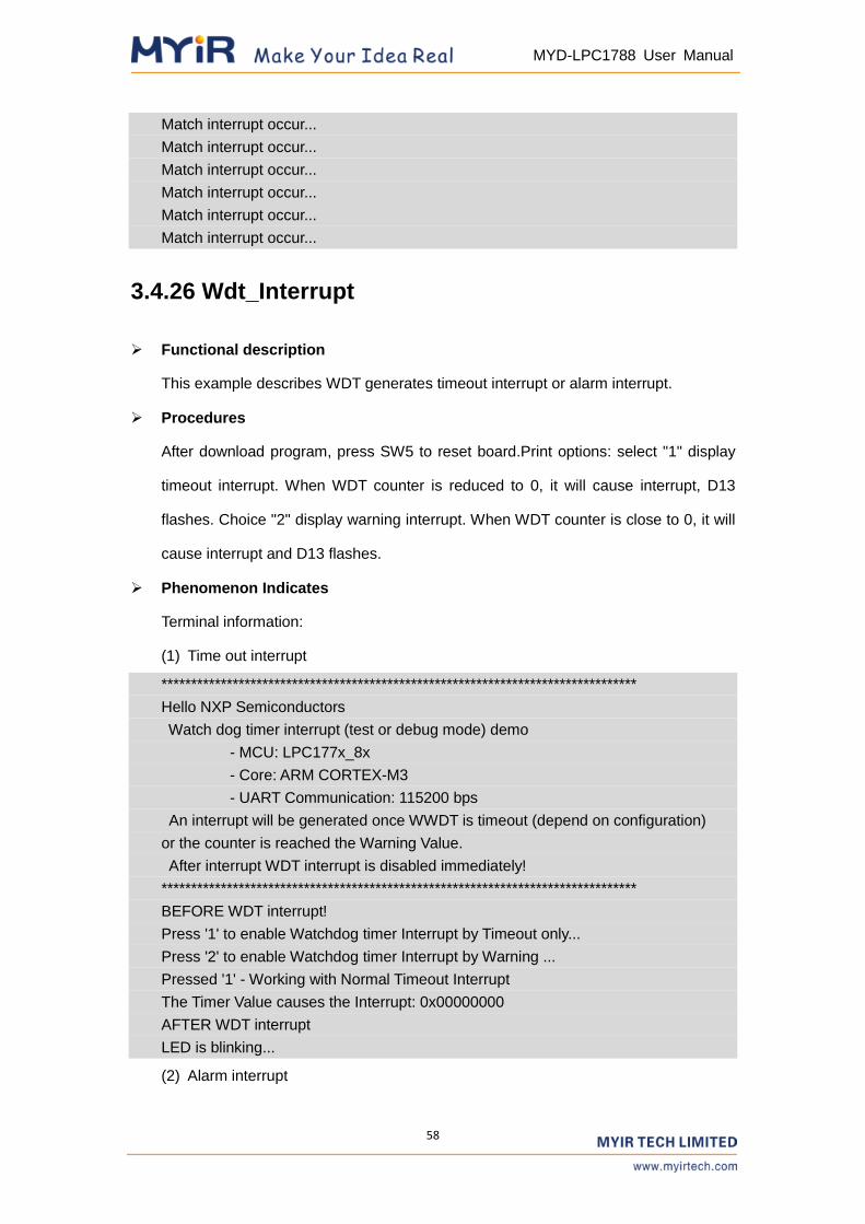
3.4.26 Wdt_Interrupt
Functional description
This example describes WDT generates timeout interrupt or alarm interrupt.
Procedures
After download program, press SW5 to reset board.Print options: select "1" display
timeout interrupt. When WDT counter is reduced to 0, it will cause interrupt, D13
flashes. Choice "2" display warning interrupt. When WDT counter is close to 0, it will
cause interrupt and D13 flashes.
Phenomenon Indicates
Terminal information:
(1) Time out interrupt
********************************************************************************
Hello NXP Semiconductors
Watch dog timer interrupt (test or debug mode) demo
- MCU: LPC177x_8x
- Core: ARM CORTEX-M3
- UART Communication: 115200 bps
An interrupt will be generated once WWDT is timeout (depend on configuration)
or the counter is reached the Warning Value.
After interrupt WDT interrupt is disabled immediately!
********************************************************************************
BEFORE WDT interrupt!
Press '1' to enable Watchdog timer Interrupt by Timeout only...
Press '2' to enable Watchdog timer Interrupt by Warning ...
Pressed '1' - Working with Normal Timeout Interrupt
The Timer Value causes the Interrupt: 0x00000000
AFTER WDT interrupt
LED is blinking...
(2) Alarm interrupt
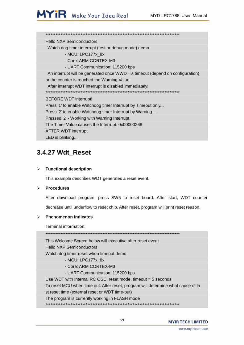
59
MYD-LPC1788 User Manual
********************************************************************************
Hello NXP Semiconductors
Watch dog timer interrupt (test or debug mode) demo
- MCU: LPC177x_8x
- Core: ARM CORTEX-M3
- UART Communication: 115200 bps
An interrupt will be generated once WWDT is timeout (depend on configuration)
or the counter is reached the Warning Value.
After interrupt WDT interrupt is disabled immediately!
********************************************************************************
BEFORE WDT interrupt!
Press '1' to enable Watchdog timer Interrupt by Timeout only...
Press '2' to enable Watchdog timer Interrupt by Warning ...
Pressed '2' - Working with Warning Interrupt
The Timer Value causes the Interrupt: 0x00000268
AFTER WDT interrupt
LED is blinking...
3.4.27 Wdt_Reset
Functional description
This example describes WDT generates a reset event.
Procedures
After download program, press SW5 to reset board. After start, WDT counter
decrease until underflow to reset chip. After reset, program will print reset reason.
Phenomenon Indicates
Terminal information:
********************************************************************************
This Welcome Screen below will executive after reset event
Hello NXP Semiconductors
Watch dog timer reset when timeout demo
- MCU: LPC177x_8x
- Core: ARM CORTEX-M3
- UART Communication: 115200 bps
Use WDT with Internal RC OSC, reset mode, timeout = 5 seconds
To reset MCU when time out. After reset, program will determine what cause of la
st reset time (external reset or WDT time-out)
The program is currently working in FLASH mode
********************************************************************************
60
MYD-LPC1788 User Manual
Last MCU reset caused by External!
********************************************************************************
This Welcome Screen below will executive after reset event
Hello NXP Semiconductors
Watch dog timer reset when timeout demo
- MCU: LPC177x_8x
- Core: ARM CORTEX-M3
- UART Communication: 115200 bps
Use WDT with Internal RC OSC, reset mode, timeout = 5 seconds
To reset MCU when time out. After reset, program will determine what cause of la
st reset time (external reset or WDT time-out)
The program is currently working in FLASH mode
********************************************************************************
Last MCU reset caused by WDT TimeOut!
3.4.28 Lcd_LQ043T3DX0A
Functional description
This example project describes LCD module displays a static picture.
Procedures
After download program, press SW5 to reset board, picture is displayed in LCD.
Phenomenon Indicates
After download program, there is picture on LCD.
3.4.29Lcd_touch
Functional description
This example project describes how to use Touch Screen and LCD。
Procedures
After download program, press SW5 to reset board, LCD screen display different
colors. Displaydifferent color on LCD screen byclicking the color block.
Phenomenon Indicates
After download program, there is picture on LCD.
3.4.30 Mci_CidCard
61
MYD-LPC1788 User Manual
Functional description
This example describes Multimedia Card Interface (MCI).
Procedures
After download program, press SW5 to reset board.Insert SD Card and read SD
cardinformation and print information in the terminal.
Phenomenon Indicates
Terminal information:
********************************************************************************
Hello NXP Semiconductors
MCI CID Card
- MCU: LPC177x_8x
- Core: ARM CORTEX-M3
- UART Communication: 115200 bps
This example is used to test the Multimedia Card Interface (MCI) function.
It is able to check, show the CID that retrieved from the card
*******************************************************************************
Currently the SD CARD is being used
- Manufacture ID: 0x00000003
- OEM/Application ID: 0x00005344
- Product Name: 0x5355303247
- Product Revision: 0x00000080
- Product Serial Number: 0x17915B1F
- Manufacturing Date: 0x000000C3
3.4.31 Usb_MassStorage
Functional description
This example describes USB Mass Storage application
Procedures
After download program, press SW5 to reset board.Connect board (J10) to PC by
Mini USB. Load “LPC1788”memory automatically and open device, there will be a
README.TXT file.
Phenomenon Indicates
Refer to figure 3-32:
62
MYD-LPC1788 User Manual
Figure 3-32
3.4.32 Usb_VirtualCom
Functional description
This example describes configure USB as virtual COM port.
Procedures
After download program and connect J10 to PC by Mini USB, press SW5 to reset
board.
Phenomenon Indicates
After download program, press SW5 to reset board.There appears "new equipment"
prompt. Select "install from a list or specified location andlocal project directory. After
install driver, "LPC177x_8x USB VCom Port (COMx)" will appear. "X" in the "COMx"
is not fixed and is changed with differentconfiguration. Refer to figure 3-33:
63
MYD-LPC1788 User Manual
Figure 3-33
3.4.33 I2S_Audio
Functional description
This example describes I2S transfers audio data to play a short music.
Procedures
After download program, press SW5 to reset board, when insert microphoneto J5
interface, there will be sound.
Phenomenon Indicates
Terminal information:
********************************************************************************
Hello NXP Semiconductors
USB MassStorage example:
- MCU: LPC177x_8x
- Core: ARM CORTEX-M3
- Communicate via: UART2 - 115200 bps
64
MYD-LPC1788 User Manual
********************************************************************************
Init UART2 for debug ...
UDA1380 Soft Reset OK!
Init UDA1380 registers step 1 OK!
Init UDA1380 registers step 2 OK!
Init UDA1380 registers step 3 OK!
Init UDA1380...
Init LPC_I2S...
Demo start...
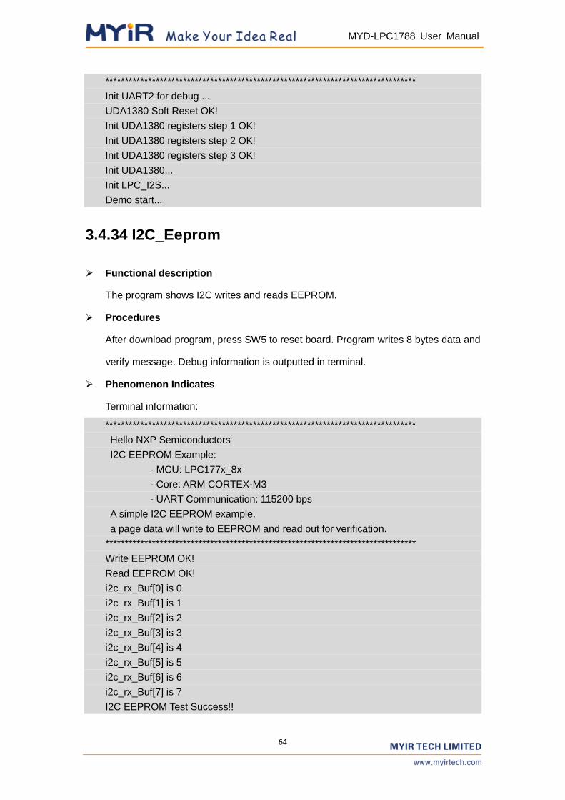
3.4.34 I2C_Eeprom
Functional description
The program shows I2C writes and reads EEPROM.
Procedures
After download program, press SW5 to reset board. Program writes 8 bytes data and
verify message. Debug information is outputted in terminal.
Phenomenon Indicates
Terminal information:
********************************************************************************
Hello NXP Semiconductors
I2C EEPROM Example:
- MCU: LPC177x_8x
- Core: ARM CORTEX-M3
- UART Communication: 115200 bps
A simple I2C EEPROM example.
a page data will write to EEPROM and read out for verification.
********************************************************************************
Write EEPROM OK!
Read EEPROM OK!
i2c_rx_Buf[0] is 0
i2c_rx_Buf[1] is 1
i2c_rx_Buf[2] is 2
i2c_rx_Buf[3] is 3
i2c_rx_Buf[4] is 4
i2c_rx_Buf[5] is 5
i2c_rx_Buf[6] is 6
i2c_rx_Buf[7] is 7
I2C EEPROM Test Success!!
65
MYD-LPC1788 User Manual
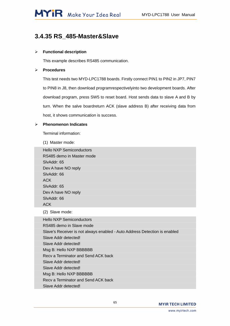
3.4.35 RS_485-Master&Slave
Functional description
This example describes RS485 communication.
Procedures
This test needs two MYD-LPC1788 boards. Firstly connect PIN1 to PIN2 in JP7, PIN7
to PIN8 in J8, then download programrespectivelyinto two development boards. After
download program, press SW5 to reset board. Host sends data to slave A and B by
turn. When the salve boardreturn ACK (slave address B) after receiving data from
host, it shows communication is success.
Phenomenon Indicates
Terminal information:
(1) Master mode:
Hello NXP Semiconductors
RS485 demo in Master mode
SlvAddr: 65
Dev A have NO reply
SlvAddr: 66
ACK
SlvAddr: 65
Dev A have NO reply
SlvAddr: 66
ACK
(2) Slave mode:
Hello NXP Semiconductors
RS485 demo in Slave mode
Slave's Receiver is not always enabled - Auto Address Detection is enabled
Slave Addr detected!
Slave Addr detected!
Msg B: Hello NXP BBBBBB
Recv a Terminator and Send ACK back
Slave Addr detected!
Slave Addr detected!
Msg B: Hello NXP BBBBBB
Recv a Terminator and Send ACK back
Slave Addr detected!
66
MYD-LPC1788 User Manual
Slave Addr detected!
Msg B: Hello NXP BBBBBB
Recv a Terminator and Send ACK back
67
MYD-LPC1788 User Manual
Appendix 1sales FAQ and technical support
How to buy
We accept paypal payment and bank wire transfer
1.Paypal payment
Please select the products add into shopping cart, the checkout web page will redirect to
paypal.com for you payment. Shipment fee will calculated automatically by your
locationregion.
2.Bank wire transfer
Pls email or fax us with products list you want, we will send you a pro-invoice with order value
total, shipping cost and bank information.
Shipping details
Please select the shipping area catalogue for you location. If you have carrier account to pay the
shipment fee, please select “Freight collect” and email us the carrier account.
Please visit http://www.myirtech.com/support.asp for more details
Noted
1.The shipment will start in 3 biz days by Fedex Express, it usually take 7 days to reach regular
cities or regions.
2.We will use DHL Express for West asia or middle east countries, it usually take 7 days to reach
regular cities or regions.
3.The remote regions defined by Fedex/DHL may cause delay, 14 days in generally.
4.Some countries have strict import policy, we will help to make shipping invoice with you
requirement, like invoice value, trade term, custom statements and H.S code etc. Please contact
us with these shipment requirements if your country has strict custom affairs.
Support and maintains
MYIR provides 12 months warranty for hardware products if the defects or failures were
notcaused by wrong use.
Return steps for defective products
1. Please email or call us get a Return Merchandise Authorization (RMA) by providing purchase
details and reasons for return (defective, incorrect etc).
2. MYIR will make a shipping invoice (list value total, item description etc) for you return request.
China have strict limit on return products, so please use MYIR’s shipping invoice to return items
to avoid custom delay.
Contact:
Tel:+86-0755-25622735 Fax: +86-0755-2553 2724
Mail to: [email protected]@myirtech.com
Website: www.myirtech.com