Embed Size (px)
Citation preview

1Rev. 1.0, July 09, 2019
MX25V5126F
P/N: PM2605 Macronix Proprietary
Key Features •VoltlageRangeVCC:2.3V-3.6V
•DualI/OSupported •UniqueID •SupportconditionalacceleratedtBEandtCE •EnhancedProgramandEraseperformance(forincreasedfactory
productionthroughput)
MX25V5126F2.3V-3.6V, 512K-BIT [x 1/x 2] CMOS SERIAL NOR FLASH

2Rev. 1.0, July 09, 2019
MX25V5126F
P/N: PM2605 Macronix Proprietary
Contents1. FEATURES .............................................................................................................................................................. 4
GENERAL ............................................................................................................................................................. 4PERFORMANCE .................................................................................................................................................. 4SOFTWARE FEATURES ...................................................................................................................................... 4HARDWARE FEATURES ...................................................................................................................................... 4
2. GENERAL DESCRIPTION ..................................................................................................................................... 53. PIN CONFIGURATIONS .......................................................................................................................................... 6
8-LAND USON (2x3mm) ...................................................................................................................................... 68-PIN TSSOP (173mil) ......................................................................................................................................... 68-PIN SOP (150mil) .............................................................................................................................................. 6
4. PIN DESCRIPTION .................................................................................................................................................. 65. BLOCK DIAGRAM ................................................................................................................................................... 76. DATA PROTECTION ................................................................................................................................................ 8
Table 1. Protected Area Sizes ............................................................................................................................... 87. MEMORY ORGANIZATION ..................................................................................................................................... 9
Table 2. Memory Organization ............................................................................................................................. 98. DEVICE OPERATION ............................................................................................................................................ 109. Timing Analysis .................................................................................................................................................... 11
Table 3. COMMAND DESCRIPTION .................................................................................................................. 129-1. Write Enable (WREN) .............................................................................................................................. 139-2. Write Disable (WRDI) ............................................................................................................................... 149-3. Factory Mode Enable (FMEN) ................................................................................................................. 159-4. ReadIdentification(RDID) ....................................................................................................................... 169-5. Read Electronic Manufacturer ID & Device ID (REMS) ........................................................................... 179-6. ID Read .................................................................................................................................................... 18Table4.IDDefinitions ........................................................................................................................................ 189-7. Read Status Register (RDSR) ................................................................................................................. 19Status Register .................................................................................................................................................... 21Table 5. Status Register ...................................................................................................................................... 219-8. Write Status Register (WRSR) ................................................................................................................. 22Table 6. Protection Modes ................................................................................................................................... 239-9. Read Data Bytes (READ) ........................................................................................................................ 269-10. Read Data Bytes at Higher Speed (FAST_READ) .................................................................................. 279-11. Dual Read Mode (DREAD) ...................................................................................................................... 289-12. 2 x I/O Read Mode (2READ) ................................................................................................................... 299-13. Sector Erase (SE) .................................................................................................................................... 309-14. Block Erase (BE32K) ............................................................................................................................... 319-15. Block Erase (BE) ..................................................................................................................................... 329-16. Chip Erase (CE) ....................................................................................................................................... 339-17. Page Program (PP) ................................................................................................................................. 349-18. Deep Power-down (DP) ........................................................................................................................... 359-19. Release from Deep Power-down (RDP), Read Electronic Signature (RES) ........................................... 369-20. Software Reset - Reset-Enable (RSTEN) and Reset (RST) .................................................................... 38

3Rev. 1.0, July 09, 2019
MX25V5126F
P/N: PM2605 Macronix Proprietary
10. POWER-ON STATE ............................................................................................................................................. 3911. ELECTRICAL SPECIFICATIONS ........................................................................................................................ 40
ABSOLUTE MAXIMUM RATINGS ...................................................................................................................... 40CAPACITANCE TA = 25°C, f = 1.0 MHz .............................................................................................................. 40Table 7. DC CHARACTERISTICS ...................................................................................................................... 42Table 8. AC CHARACTERISTICS ...................................................................................................................... 43
12. RECOMMENDED OPERATING CONDITIONS ................................................................................................... 45Table 9. Power-Up/Down Voltage and Timing ..................................................................................................... 4712-1. Initial Delivery State ................................................................................................................................. 47
13. ERASE AND PROGRAMMING PERFORMANCE (2.3V - 3.6V) ........................................................................ 4814. ERASE AND PROGRAMMING PERFORMANCE (Factory Mode) ................................................................... 4815. DATA RETENTION .............................................................................................................................................. 4816. LATCH-UP CHARACTERISTICS ........................................................................................................................ 4817. ORDERING INFORMATION ................................................................................................................................ 4918. PART NAME DESCRIPTION ............................................................................................................................... 5019. PACKAGE INFORMATION .................................................................................................................................. 51
19-1. 8-USON (2x3mm) .................................................................................................................................... 5119-2. 8-pin TSSOP (173mil) .............................................................................................................................. 5219-3. 8-pin SOP (150mil) .................................................................................................................................. 53
20. REVISION HISTORY ........................................................................................................................................... 54

4Rev. 1.0, July 09, 2019
MX25V5126F
P/N: PM2605 Macronix Proprietary
GENERAL• Supports Serial Peripheral Interface - Mode 0 and Mode 3
• 524,288x1bitstructureor262,144x2bits(DualOutputmode) Structure
• Equal Sectors with 4K byte each, or Equal Blocks with32K/64K byte each
- Any Block can be erased individually
• SinglePowerSupplyOperation - 2.3 to 3.6 volt for read, erase, and program operations• Latch-upprotectedto100mAfrom-1VtoVcc+1V
PERFORMANCE • HighPerformance - Fast Read: - 1 I/O: 80MHz with 8 dummy cycles (2.7V-3.6V) 50MHz with 8 dummy cycles (2.3V-2.7V) - 2 I/O: 80MHz with 4 dummy cycles (2.7V-3.6V) 50MHz with 4 dummy cycles (2.3V-2.7V) - Fast program time: 1.6ms /page (256-byte) - Byte program time: 20us - Fast erase time: 50ms(typ.)/sector (4K-byte per sector); 0.3s(typ.)/block (32K-byte per block); 0.6s(typ.)/block (64K-byte per block); 1.8s(typ.)/chip.
•LowPowerConsumption - Low active read current: 6mA(max.) at 50MHz - Low active programming current: 5mA (typ.)/page - Low active sector erase current: 5mA (typ.) - Low standby current: 5uA (typ.) - Deep power-down mode: 1uA (typ.)
•Minimum100,000erase/programcycles•20yearsdataretention
2.3V-3.6V 512K-BIT [x 1/x 2] CMOS SERIAL FLASH 1. FEATURES
SOFTWARE FEATURES• InputDataFormat:1-byteCommandcode• BlockLockprotection:TheBP0-BP3statusbitdefines
the size of the area to be software protected against Program and Erase instructions.
• AutoEraseandAutoProgramAlgorithm - Automatically erases and verifies data at selected
sector -Automaticallyprogramsandverifiesdataatselected
page by an internal algorithm that automatically times the program pulse widths (Any page to be programed shouldhavepageintheerasedstatefirst)
• Status Register Feature• ElectronicIdentification - JEDEC 2-byte Device ID - RES command, 1-byte Device ID• SupportUniqueID(PleasecontactlocalMacronixsales for detail information)
HARDWARE FEATURES• SCLK Input - Serial clock input• SI/SIO0 - Serial Data Input or Serial Data Output for Dual
output mode• SO/SIO1 - Serial Data Output or Serial Data Output for Dual
output mode• WP#pin - Hardware write protection• PACKAGE - 8-USON (2x3mm)
- 8-pin TSSOP (173mil)
- 8-pin SOP (150mil)
All devices are RoHS compliant and Halogen-free

5Rev. 1.0, July 09, 2019
MX25V5126F
P/N: PM2605 Macronix Proprietary
2. GENERAL DESCRIPTION
MX25V5126F is a CMOS 512Kb bits Serial NOR Flash memory, which is configured as 65,536 x 8 internally. MX25V5126F features a serial peripheral interface and software protocol allowing operation on a simple 3-wire bus. The three bus signals are a clock input (SCLK), a serial data input (SI), and a serial data output (SO). Serial access tothedeviceisenabledbyCS#input.
MX25V5126Fprovidessequentialreadoperationonthewholechip.
After program/erase command is issued, auto program/erase algorithms which program/erase and verify the specified page or sector/block locations will be executed. Program command is executed on page (256 bytes)basis. Erase command is executed on chip or on 4K-byte sector, or 32KB block (32K-byte), or 64K-byte block, or whole chip basis.
To provide user with ease of interface, a status register is included to indicate the status of the chip. The status read command can be issued to detect completion status of a program or erase operation via WIP bit.
WhenthedeviceisnotinoperationandCS#ishigh,itisputinstandbymode.
The MX25V5126F utilizes Macronix's proprietary memory cell, which reliably stores memory contents even after 100,000 program and erase cycles.

6Rev. 1.0, July 09, 2019
MX25V5126F
P/N: PM2605 Macronix Proprietary
3. PIN CONFIGURATIONS
SYMBOL DESCRIPTIONCS# Chip Select
SI/SIO0 Serial Data Input (for 1 x I/O)/ Serial Data Input & Output (for Dual output mode)
SO/SIO1 Serial Data Output (for 1 x I/O)/ Serial Data Input & Output (for Dual output mode)
SCLK Clock InputWP# Write ProtectionVCC +3.3VPowerSupplyGND Ground
4. PIN DESCRIPTION
8-LAND USON (2x3mm)
1234
CS#SO/SIO1
WP#GND
8765
VCCNCSCLKSI/SIO0
8-PIN TSSOP (173mil)
1234
CS#SO/SIO1
WP#GND
VCCNCSCLKSI/SIO0
8765
8-PIN SOP (150mil)
1234
CS#SO/SIO1
WP#GND
VCCNCSCLKSI/SIO0
8765
Note: The pin of WP# will remain internal pull upfunction while this pin is not physically connected insystemconfiguration.However,theinternalpullupfunctionwillbedisabledifthesystemhasphysicalconnectiontoWP#pin.

7Rev. 1.0, July 09, 2019
MX25V5126F
P/N: PM2605 Macronix Proprietary
5. BLOCK DIAGRAM
AddressGenerator
Memory Array
Y-Decoder
X-D
ecoder
DataRegister
SRAMBuffer
SI/SIO0 SO/SIO1
CS# WP#
SCLK Clock Generator
StateMachine
ModeLogic
SenseAmplifier
HVGenerator
OutputBuffer

8Rev. 1.0, July 09, 2019
MX25V5126F
P/N: PM2605 Macronix Proprietary
6. DATA PROTECTION
During power transition, there may be some false system level signals which result in inadvertent erasure or programming. The device is designed to protect itself from these accidental write cycles.
The state machine will be reset as standby mode automatically during power up. In addition, the control register architecture of the device constrains that the memory contents can only be changed after specific commandsequenceshavecompletedsuccessfully.
In the following, there are several features to protect the system from the accidental write cycles during VCC power-up and power-down or from system noise.
• Valid command length checking: The command length will be checked whether it is at byte base and completed on byte boundary.
• Write Enable (WREN) command: WRENcommandisrequiredtosettheWriteEnableLatchbit(WEL)beforeother command to change data.
• Deep Power Down Mode: By entering deep power down mode, the flash device also is under protectedfrom writing all commands except Release from Deep Power-down mode command (RDP), Read Electronic Signature command (RES), power-cycle, or reset. For more details, please refer to "9-18.DeepPower-down(DP)" section.
•Protection Features: There are some protection features that could protect content change from unintentional write and hostile access:
A. The software Protection Mode (SPM) - Use BP0, BP1, BP3 bits to set the part of memory to be protected as read only
Thedefinitionofprotectareaisshownas "Table1.ProtectedAreaSizes". B. Hardware Protection Mode (HPM) - useWP#bysettingWP#goinglowtoprotecttheBP0,BP1,BP3bitsandstatus
register write protection (SRWD).
Table 1. Protected Area Sizes
Status bit Protect level 512Kb BP3 BP2 BP1 BP00 X 0 0 0 (none) None0 X 0 1 1 (1 block) All0 X 1 0 2 (1 block) All0 X 1 1 3 (1 block) All1 X 0 0 0 (none) None1 X 0 1 1 (1 block) All1 X 1 0 2 (1 block) All1 X 1 1 3 (1 block) All
Note: X means “Don’t Care”

9Rev. 1.0, July 09, 2019
MX25V5126F
P/N: PM2605 Macronix Proprietary
Table 2. Memory Organization
Block(64KB)
Block(32KB)
Sector(4KB)
Address Range
0
1
|
0
15 00F000h 00FFFFh: : :3 003000h 003FFFh2 002000h 002FFFh1 001000h 001FFFh0 000000h 000FFFh
7. MEMORY ORGANIZATION
10Rev. 1.0, July 09, 2019
MX25V5126F
P/N: PM2605 Macronix Proprietary
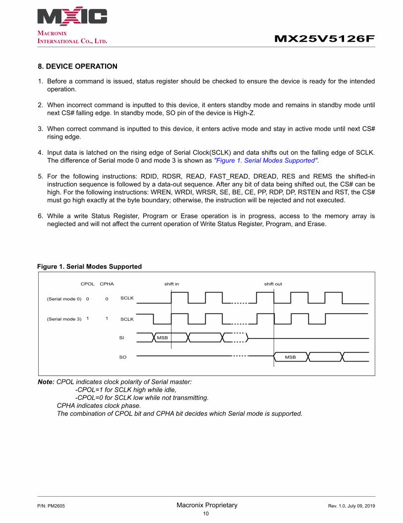
8. DEVICE OPERATION
1. Before a command is issued, status register should be checked to ensure the device is ready for the intended operation.
2. When incorrect command is inputted to this device, it enters standby mode and remains in standby mode until nextCS#fallingedge.Instandbymode,SOpinofthedeviceisHigh-Z.
3. Whencorrectcommandisinputtedtothisdevice,itentersactivemodeandstayinactivemodeuntilnextCS#rising edge.
4. Input data is latched on the rising edge of Serial Clock(SCLK) and data shifts out on the falling edge of SCLK. The difference of Serial mode 0 and mode 3 is shown as "Figure1.SerialModesSupported".
5. For the following instructions: RDID, RDSR, READ, FAST_READ, DREAD, RES and REMS the shifted-in instructionsequenceisfollowedbyadata-outsequence.Afteranybitofdatabeingshiftedout,theCS#canbehigh.Forthefollowinginstructions:WREN,WRDI,WRSR,SE,BE,CE,PP,RDP,DP,RSTENandRST,theCS#must go high exactly at the byte boundary; otherwise, the instruction will be rejected and not executed.
6. While a write Status Register, Program or Erase operation is in progress, access to the memory array is neglected and will not affect the current operation of Write Status Register, Program, and Erase.
Figure 1. Serial Modes Supported
SCLK
MSB
CPHA shift in shift out
SI
0
1
CPOL
0(Serial mode 0)
(Serial mode 3) 1
SO
SCLK
MSB
Note: CPOLindicatesclockpolarityofSerialmaster:-CPOL=1forSCLKhighwhileidle,-CPOL=0forSCLKlowwhilenottransmitting.
CPHAindicatesclockphase.ThecombinationofCPOLbitandCPHAbitdecideswhichSerialmodeissupported.
11Rev. 1.0, July 09, 2019
MX25V5126F
P/N: PM2605 Macronix Proprietary
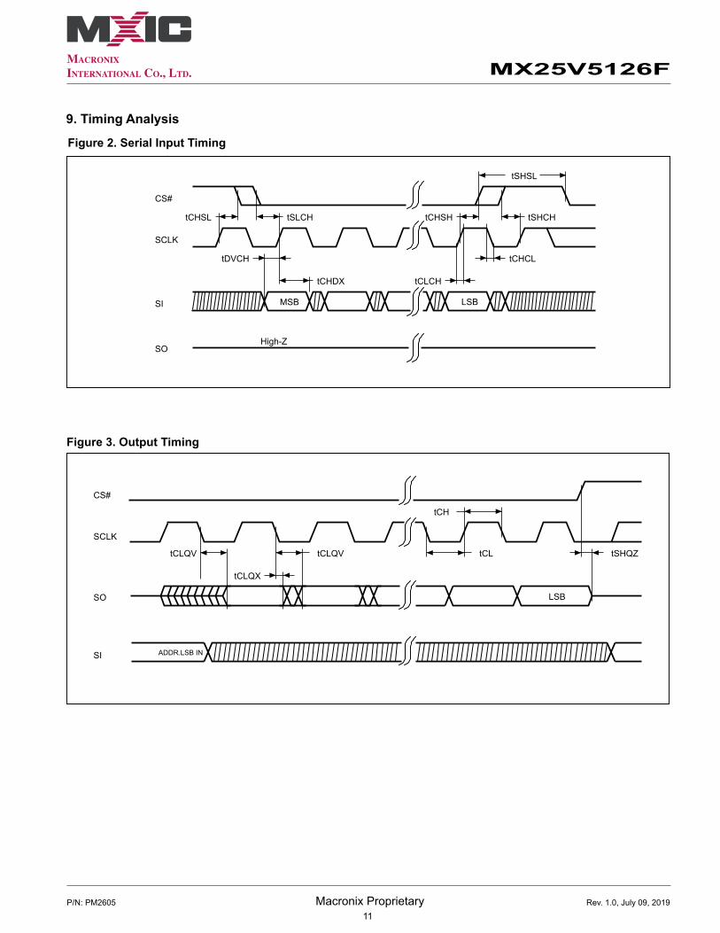
Figure 2. Serial Input Timing
Figure 3. Output Timing
LSB
ADDR.LSB IN
tSHQZ
tCH
tCL
tCLQX
tCLQVtCLQV
SCLK
SO
CS#
SI
SCLK
SI
CS#
MSB
SO
tDVCH
High-Z
LSB
tSLCH
tCHDX
tCHCL
tCLCH
tSHCH
tSHSL
tCHSHtCHSL
9. Timing Analysis

12Rev. 1.0, July 09, 2019
MX25V5126F
P/N: PM2605 Macronix Proprietary
Table 3. COMMAND DESCRIPTION
Notes: 1)ADD=00Hwilloutputthemanufacturer'sIDfirstandADD=01HwilloutputdeviceIDfirst.2)Itisnotrecommendedtoadoptanyothercodewhichisnotinthecommanddefinitiontableabove.3)TheRSTENcommandmustbeexecutedbeforeexecutingtheRSTcommand. Ifanyothercommandis issued in-between
RSTENandRST,theRSTcommandwillbeignored.
COMMAND (byte) I/O 1st byte 2nd byte 3rd byte 4th byte 5th byte ActionRead/Write Array
READ (Normal Read)
1 03 (hex) ADD1 ADD2 ADD3 n bytes read out until CS#goeshigh
Fast Read (Fast Read Data)
1 0B (hex) ADD1 ADD2 ADD3 Dummy n bytes read out until CS#goeshigh
DREAD (1 x I / 2O Read Command)
2 3B (hex) ADD1 ADD2 ADD3 Dummy n bytes read out by Dual OutputuntilCS#goeshigh
2READ (2 x I/O Read Command)
2 BB (hex) ADD1 ADD2 ADD3 Dummy n bytes read out by 2 x I/OuntilCS#goeshigh
SE (Sector Erase)
1 20 (hex) ADD1 ADD2 ADD3 Erase the selected sector
BE 32K (Block Erase 32KB)
1 52 (hex) ADD1 ADD2 ADD3 Erase the selected 32KB block
BE (Block Erase 64KB)
1 D8 (hex) ADD1 ADD2 ADD3 Erase the selected 64KB block
CE (Chip Erase)
1 60 or C7 (hex)
Erase the whole chip
PP (Page Program)
1 02 (hex) ADD1 ADD2 ADD3 Program the selected page
Register/Setting
WREN (Write Enable)
1 06 (hex) Set the (WEL) write enable latch bit
WRDI (Write Disable)
1 04 (hex) Reset the (WEL) write enable latch bit
FMEN (Factory mode enable)
1 41 (hex) Enable factory mode
RDSR (Read Status Register)
1 05 (hex) Read out the status register
WRSR (Write Status Register)
1 01 (hex) Write new values to the status register
DP (Deep Power- down)
1 B9 (hex) Enter deep power down mode
RDP (Release from deep power down)
1 AB (hex) release from deep power down mode
ID/Reset RDID (Read Identification)
1 9F (hex) Output manufacturer ID and 2-byte device ID
RES (Read Electronic ID)
1 AB (hex) x x x Read out 1-byte Device ID
REMS (Read Electronic Manufacturer & Device ID)
1 90 (hex) x x ADD
(Note1)Output the manufacturer ID and device ID
RSTEN (Reset Enable)
1 66 (hex)
RST (Reset Memory)
1 99 (hex) (Note3)

13Rev. 1.0, July 09, 2019
MX25V5126F
P/N: PM2605 Macronix Proprietary
9-1. Write Enable (WREN)
The Write Enable (WREN) instruction is for setting Write Enable Latch (WEL) bit. For those instructions like PP, SE, BE32K, BE, CE, and WRSR, which are intended to change the device content WEL bit should be set every time after the WREN instruction setting the WEL bit.
ThesequenceofissuingWRENinstructionis:CS#goeslow→sendWRENinstructioncode→CS#goeshigh.
The SIO[1:0] are "don't care" .
Figure 4. Write Enable (WREN) Sequence
21 3 4 5 6 7
High-Z
0
06h
Command
SCLK
SI
CS#
SO
Mode 3
Mode 0

14Rev. 1.0, July 09, 2019
MX25V5126F
P/N: PM2605 Macronix Proprietary
9-2. Write Disable (WRDI)
The Write Disable (WRDI) instruction is to reset Write Enable Latch (WEL) bit.
ThesequenceofissuingWRDIinstructionis:CS#goeslow→sendWRDIinstructioncode→CS#goeshigh.
The SIO[1:0] are "don't care".
The WEL bit is reset by following situations: - Power-up - Completion of Write Disable (WRDI) instruction - Completion of Write Status Register (WRSR) instruction - Completion of Page Program (PP) instruction - Completion of Sector Erase (SE) instruction - Completion of Block Erase 32KB (BE32K) instruction - Completion of Block Erase (BE) instruction - Completion of Chip Erase (CE) instruction - Completion of Softreset (RSTEN & RST) instruction
Figure 5. Write Disable (WRDI) Sequence
21 3 4 5 6 7
High-Z
0Mode 3
Mode 0
04h
Command
SCLK
SI
CS#
SO

15Rev. 1.0, July 09, 2019
MX25V5126F
P/N: PM2605 Macronix Proprietary
9-3. Factory Mode Enable (FMEN)
The Factory Mode Enable (FMEN) instruction is for enhance Program and Erase performance for increase factory production throughput. The FMEN instruction need to combine with the instructions which are intended to change the device content, like PP, SE, BE32K, BE, and CE.
ThesequenceofissuingFMENinstructionis:CS#goeslow→sendingFMENinstructioncode→CS#goeshigh.Avalidfactorymodeoperationneedtoincludedthreesequences:WRENinstruction→FMENinstruction→Programor Erase instruction.
The FMEN is reset by following situations - Power-up - PP command completion - SE command completion - BE32K command completion - BE command completion - CE command completion - Softreset command completion
Figure 6. Factory Mode Enable (FMEN) Sequence
21 3 4 5 6 7
High-Z
0
41h
Command
SCLK
SI
CS#
SO
Mode 3
Mode 0

16Rev. 1.0, July 09, 2019
MX25V5126F
P/N: PM2605 Macronix Proprietary
9-4. Read Identification (RDID)
The RDID instruction is for reading the manufacturer ID of 1-byte and followed by Device ID of 2-byte. The Macronix Manufacturer ID and Device ID are listed as "Table4.IDDefinitions". ThesequenceofissuingRDIDinstructionis:CS#goeslow→sendRDIDinstructioncode→24-bitsIDdataoutonSO→toendRDIDoperationcandriveCS#tohighatanytimeduringdataout.
While Program/Erase operation is in progress, it will not decode the RDID instruction, therefore there's no effect on thecycleofprogram/eraseoperationwhichiscurrentlyinprogress.WhenCS#goeshigh,thedeviceisatstandbystage.
Figure 7. Read Identification (RDID) Sequence
21 3 4 5 6 7 8 9 10 11 12 13 14 15
Command
0
Manufacturer IdentificationHigh-Z
MSB
15 14 13 3 2 1 0
Device Identification
MSB
7 6 5 3 2 1 0
16 17 18 28 29 30 31SCLK
SI
CS#
SO
9Fh
Mode 3
Mode 0

17Rev. 1.0, July 09, 2019
MX25V5126F
P/N: PM2605 Macronix Proprietary
9-5. Read Electronic Manufacturer ID & Device ID (REMS)
The REMS instruction returns both the JEDEC assigned manufacturer ID and the device ID. The Device ID values are listed in "Table4.IDDefinitions".
TheREMSinstructionisinitiatedbydrivingtheCS#pinlowandsendingtheinstructioncode"90h"followedbytwodummy bytes and one address byte (A7~A0). After which the manufacturer ID for Macronix (C2h) and the device IDareshiftedoutonthefallingedgeofSCLKwiththemostsignificantbit (MSB)first. If theaddressbyte is00h,themanufacturerIDwillbeoutputfirst,followedbythedeviceID.Iftheaddressbyteis01h,thenthedeviceIDwillbeoutputfirst, followedbythemanufacturerID.WhileCS#is low,themanufactureranddeviceIDscanbereadcontinuously,alternatingfromonetotheother.TheinstructioniscompletedbydrivingCS#high.
Figure 8. Read Electronic Manufacturer & Device ID (REMS) Sequence
15 14 13 3 2 1 0
21 3 4 5 6 7 8 9 10
2 Dummy Bytes
0
32 33 34 36 37 38 39 40 41 42 43 44 45 46
7 6 5 4 3 2 01
Manufacturer ID
ADD (1)
MSB
7 6 5 4 3 2 1 0
Device ID
MSB MSB
7
47
7 6 5 4 3 2 01
3531302928
SCLK
SI
CS#
SO
SCLK
SI
CS#
SO
90h
High-Z
Command
Mode 3
Mode 0
Note: (1) ADD=00Hwilloutputthemanufacturer'sIDfirstandADD=01HwilloutputdeviceIDfirst.
18Rev. 1.0, July 09, 2019
MX25V5126F
P/N: PM2605 Macronix Proprietary
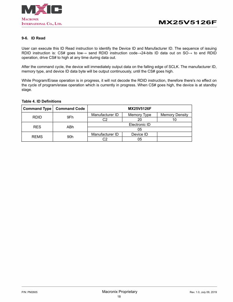
9-6. ID Read
User can execute this ID Read instruction to identify the Device ID and Manufacturer ID. ThesequenceofissuingRDID instruction is: CS# goes low→ send RDID instruction code→24-bits ID data out on SO→ to end RDIDoperation,driveCS#tohighatanytimeduringdataout.
After the command cycle, the device will immediately output data on the falling edge of SCLK. The manufacturer ID, memorytype,anddeviceIDdatabytewillbeoutputcontinuously,untiltheCS#goeshigh.
While Program/Erase operation is in progress, it will not decode the RDID instruction, therefore there's no effect on thecycleofprogram/eraseoperationwhichiscurrentlyinprogress.WhenCS#goeshigh,thedeviceisatstandbystage.
Table 4. ID Definitions
Command Type Command Code MX25V5126F
RDID 9Fh Manufacturer ID Memory Type Memory DensityC2 20 10
RES ABh Electronic ID05
REMS 90h Manufacturer ID Device IDC2 05

19Rev. 1.0, July 09, 2019
MX25V5126F
P/N: PM2605 Macronix Proprietary
9-7. Read Status Register (RDSR)
The RDSR instruction is for reading Status Register Bits. The Read Status Register can be read at any time (even in program/erase/write status register condition). It is recommended to check the Write in Progress (WIP) bit before sending a new instruction when a program, erase, or write status register operation is in progress.
Thesequenceof issuingRDSRinstructionis:CS#goeslow→SendRDSRinstructioncode→StatusRegisterdataout on SO.
The SIO[1:0] are "don't care".
Figure 9. Read Status Register (RDSR) Sequence
21 3 4 5 6 7 8 9 10 11 12 13 14 15
command
0
7 6 5 4 3 2 1 0
Status Register OutHigh-Z
MSB
7 6 5 4 3 2 1 0
Status Register Out
MSB
7
SCLK
SI
CS#
SO
05h
Mode 3
Mode 0

20Rev. 1.0, July 09, 2019
MX25V5126F
P/N: PM2605 Macronix Proprietary
WREN command
Program/erase command
Write program data/address(Write erase address)
RDSR command
Read array data(same address of PGM/ERS)
Program/erase successfully
Yes
YesProgram/erase fail
No
start
Verify OK?
WIP=0?
Program/erase another block?
Program/erase completedNo
Yes
No
RDSR command*
Yes
WEL=1?No
* Issue RDSR to check BP[3:0].
RDSR command
Read WEL=0, BP[3:0], and SRWD data
Figure 10. Program/Erase flow with read array data
ForusertocheckifProgram/Eraseoperationisfinishedornot,RDSRinstructionflowareshownasfollows:

21Rev. 1.0, July 09, 2019
MX25V5126F
P/N: PM2605 Macronix Proprietary
Note: 1.Pleasereferto"Table1.ProtectedAreaSizes".
bit7 bit6 bit5 bit4 bit3 bit2 bit1 bit0
SRWD (status register write
protect)Reserved
BP3 (level of
protected block)
Reserved
BP1 (level of
protected block)
BP0 (level of
protected block)
WEL(write enable
latch)
WIP(write in
progress bit)
1=status register write
disabled0=status
register write enabled
Reserved (Note1) Reserved (Note1) (Note1)
1=write enabled
0=not write enabled
1=write operation
0=not in write operation
Non-volatile bit
Non-volatile bit
Non-volatile bit
Non-volatile bit
Non-volatile bit
Non-volatile bit volatile bit volatile bit
Table 5. Status Register
Status Register
Thedefinitionsofthestatusregisterbitsisasbelow:
WIP bit. The Write in Progress (WIP) bit, a volatile bit, indicates whether the device is busy in program/erase/write status register progress. When WIP bit sets to 1, which means the device is busy in program/erase/write status register progress. When WIP bit sets to 0, which means the device is not in progress of program/erase/write status register cycle.
WEL bit. The Write Enable Latch (WEL) bit is a volatile bit that is set to “1” by the WREN instruction. WEL needs to beset to “1” before the device can accept program and erase instructions, otherwise the program and erase instructionsare ignored. WEL automatically clears to “0” when a program or erase operation completes. To ensure that both WIPand WEL are “0” and the device is ready for the next program or erase operation, it is recommended that WIP beconfirmedtobe“0”beforecheckingthatWELisalso“0”.Ifaprogramoreraseinstructionisappliedtoaprotectedmemory area, the instruction will be ignored and WEL will clear to “0”.
BP3, BP1, BP0 bits. TheBlockProtect(BP3,BP1,BP0)bits,non-volatilebits,indicatetheprotectedarea(asdefinedin "Table1.ProtectedAreaSizes") of the device to against the program/erase instruction without hardware protection modebeingset.TowritetheBlockProtect(BP3,BP1,BP0)bitsrequirestheWriteStatusRegister(WRSR)instructiontobeexecuted.ThosebitsdefinetheprotectedareaofthememorytoagainstPageProgram(PP),SectorErase(SE),Block Erase (BE) and Chip Erase(CE) instructions (only if all Block Protect bits set to 0 or BP3, BP2, BP1, BP0 are set to "1,X,0,0", the CE instruction can be executed).
SRWD bit. The Status Register Write Disable (SRWD) bit, non-volatile bit, is operated together with Write Protection(WP#)pinforprovidinghardwareprotectionmode.ThehardwareprotectionmoderequiresSRWDsetsto1andWP#pinsignalislowstage.Inthehardwareprotectionmode,theWriteStatusRegister(WRSR)instructionisnolonger accepted for execution and the SRWD bit and Block Protect bits (BP3, BP1, BP0) are read only.

22Rev. 1.0, July 09, 2019
MX25V5126F
P/N: PM2605 Macronix Proprietary
9-8. Write Status Register (WRSR)
TheWRSR instruction is forchanging thevaluesofStatusRegisterBitsandConfigurationRegisterBits.Beforesending WRSR instruction, the Write Enable (WREN) instruction must be decoded and executed to set the Write Enable Latch (WEL) bit in advance. The WRSR instruction can change the value of Block Protect (BP3, BP1, BP0) bitstodefinetheprotectedareaofmemory(asshownin"Table8.ACCHARACTERISTICS".) The WRSR can also setorresettheStatusRegisterWriteDisable(SRWD)bitinaccordancewithWriteProtection(WP#)pinsignal,buthas no effect on bit1(WEL) and bit0 (WIP) of the status register. The WRSR instruction cannot be executed once the Hardware Protected Mode (HPM) is entered.
ThesequenceofissuingWRSRinstructionis:CS#goeslow→sendWRSRinstructioncode→StatusRegisterdataonSI→CS#goeshigh.
TheCS#must go high exactly at the 16 bits data boundary; otherwise, the instructionwill be rejected and notexecuted.Theself-timedWriteStatusRegistercycletime(tW)isinitiatedassoonasChipSelect(CS#)goeshigh.The Write in Progress (WIP) bit still can be checked during the Write Status Register cycle is in progress. The WIP sets 1 during the tW timing, and sets 0 when Write Status Register Cycle is completed, and the Write Enable Latch (WEL) bit is reset.
Figure 11. Write Status Register (WRSR) Sequence
21 3 4 5 6 7 8 9 10 11 12 13 14 15
StatusRegister In
0
7 6 5 4 3 2 01
MSB
SCLK
SI
CS#
SO
01
High-Z
command

23Rev. 1.0, July 09, 2019
MX25V5126F
P/N: PM2605 Macronix Proprietary
Software Protected Mode (SPM): - WhenSRWDbit=0,nomatterWP#isloworhigh,theWRENinstructionmaysettheWELbitandcanchange
thevaluesofSRWD,BP3,BP1,BP0.Theprotectedarea,which isdefinedbyBP3,BP1,BP0, isatsoftwareprotected mode (SPM).
- WhenSRWD bit=1 andWP# is high, theWREN instructionmay set theWEL bit can change the values ofSRWD,BP3,BP1,BP0.Theprotectedarea,whichisdefinedbyBP3,BP1,BP0,isatsoftwareprotectedmode(SPM)
Note: IfSRWDbit=1butWP#islow,itisimpossibletowritetheStatusRegistereveniftheWELbithaspreviouslybeenset. It is rejected to write the Status Register and not be executed.
Hardware Protected Mode (HPM):- WhenSRWDbit=1,andthenWP#islow(orWP#islowbeforeSRWDbit=1),itentersthehardwareprotected
mode (HPM). The data of the protected area is protected by software protected mode by BP3, BP1, BP0 and hardwareprotectedmodebytheWP#toagainstdatamodification.
Note: Toexit thehardwareprotectedmoderequiresWP#drivinghighonce thehardwareprotectedmode isentered. IftheWP#pinispermanentlyconnectedtohigh,thehardwareprotectedmodecanneverbeentered;onlycanusesoftware protected mode via BP3, BP1, BP0.
Table 6. Protection Modes
Note: 1.AsdefinedbythevaluesintheBlockProtect(BP3,BP1,BP0)bitsoftheStatusRegister,asshowninthetable
above.
Mode Status register condition WP# and SRWD bit status Memory
Software protectionmode (SPM)
Status register can be writtenin (WEL bit is set to "1") and
the SRWD, BP0-BP3bits can be changed
WP#=1andSRWDbit=0,orWP#=0andSRWDbit=0,or
WP#=1andSRWD=1
The protected area cannot
be program or erase.
Hardware protectionmode (HPM)
The SRWD, BP0-BP3 ofstatus register bits cannot be
changedWP#=0,SRWDbit=1
The protected area cannot
be program or erase.
24Rev. 1.0, July 09, 2019
MX25V5126F
P/N: PM2605 Macronix Proprietary
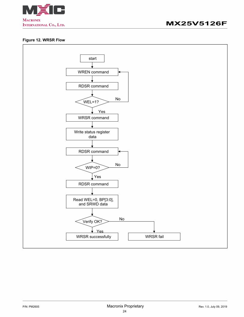
Figure 12. WRSR Flow
WREN command
WRSR command
Write status register data
RDSR command
WRSR successfully
Yes
YesWRSR fail
No
start
Verify OK?
WIP=0?No
RDSR command
Yes
WEL=1?No
RDSR command
Read WEL=0, BP[3:0], and SRWD data

25Rev. 1.0, July 09, 2019
MX25V5126F
P/N: PM2605 Macronix Proprietary
Figure 13. WP# Setup Timing and Hold Timing during WRSR when SRWD=1
High-Z
01h
0 1 2 3 4 5 6 7 8 9 10 11 12 13 14 15
tWHSLtSHWL
SCLK
SI
CS#
WP#
SO
Note: WP#mustbekepthighuntiltheembeddedoperationfinish.

26Rev. 1.0, July 09, 2019
MX25V5126F
P/N: PM2605 Macronix Proprietary
9-9. Read Data Bytes (READ)
The read instruction is for reading data out. The address is latched on rising edge of SCLK, and data shifts out on thefallingedgeofSCLKatamaximumfrequencyfR.Thefirstaddressbytecanbeatanylocation.Theaddressis automatically increased to the next higher address after each byte data is shifted out, so the whole memory can be read out at a single READ instruction. The address counter rolls over to 0 when the highest address has been reached.
Thesequenceof issuingREAD instruction is:CS#goes low→sendREAD instructioncode→3-byteaddressonSI→dataoutonSO→toendREADoperationcanuseCS#tohighatanytimeduringdataout.
Figure 14. Read Data Bytes (READ) Sequence
SCLK
SI
CS#
SO
23
21 3 4 5 6 7 8 9 10 28 29 30 31 32 33 34 35
22 21 3 2 1 0
36 37 38
7 6 5 4 3 1 70
Data Out 1
0
MSB
MSB
2
39
Data Out 2
03h
High-Z
command
Mode 3
Mode 024-Bit Address

27Rev. 1.0, July 09, 2019
MX25V5126F
P/N: PM2605 Macronix Proprietary
9-10. Read Data Bytes at Higher Speed (FAST_READ)
TheFAST_READ instruction is forquickly readingdataout.Theaddress is latchedonrisingedgeofSCLK,anddataofeachbitshiftsoutonthefallingedgeofSCLKatamaximumfrequencyfC.Thefirstaddressbytecanbeatany location. The address is automatically increased to the next higher address after each byte data is shifted out, so the whole memory can be read out at a single FAST_READ instruction. The address counter rolls over to 0 when the highest address has been reached.
ThesequenceofissuingFAST_READinstructionis:CS#goeslow→sendFAST_READinstructioncode→3-byteaddressonSI→1-dummybyte(default)addressonSI→dataoutonSO→toendFAST_READoperationcanuseCS#tohighatanytimeduringdataout.
While Program/Erase/Write Status Register cycle is in progress, FAST_READ instruction is rejected without any impact on the Program/Erase/Write Status Register current cycle.
Figure 15. Read at Higher Speed (FAST_READ) Sequence
23
21 3 4 5 6 7 8 9 10 28 29 30 31
22 21 3 2 1 0
High-Z
0
32 33 34 36 37 38 39 40 41 42 43 44 45 46
7 6 5 4 3 2 01
DATA OUT 1
Dummy Cycle
MSB
7 6 5 4 3 2 1 0
DATA OUT 2
MSB MSB
7
47
7 6 5 4 3 2 01
35
SCLK
SI
CS#
SO
SCLK
SI
CS#
SO
0Bh
Command
Mode 3
Mode 024-Bit Address

28Rev. 1.0, July 09, 2019
MX25V5126F
P/N: PM2605 Macronix Proprietary
9-11. Dual Read Mode (DREAD)
The DREAD instruction enable double throughput of Serial NOR Flash in read mode. The address is latched on rising edge of SCLK, and data of every two bits (interleave on 2 I/O pins) shift out on the falling edge of SCLK at amaximumfrequencyfT.Thefirstaddressbytecanbeatanylocation.Theaddressisautomaticallyincreasedto the next higher address after each byte data is shifted out, so the whole memory can be read out at a single DREAD instruction. The address counter rolls over to 0 when the highest address has been reached. Once writing DREAD instruction, the following data out will perform as 2-bit instead of previous 1-bit.
ThesequenceofissuingDREADinstructionis:CS#goeslow→ send DREAD instruction → 3-byte address on SI → 8-bit dummy cycle → data out interleave on SIO1 & SIO0 →toendDREADoperationcanuseCS#tohigh at any time during data out.
While Program/Erase/Write Status Register cycle is in progress, DREAD instruction is rejected without any impact on the Program/Erase/Write Status Register current cycle.
Figure 16. Dual Read Mode Sequence (Command 3Bh)
High Impedance
21 3 4 5 6 7 80
SCLK
SI/SIO0
SO/SIO1
CS#
9 30 31 32 39 40 41 43 44 4542
3B D4
D5
D2
D3D7
D6 D6 D4D0
D7 D5D1
Command 24 ADD Cycle 8 dummy cycle
A23 A22 A1 A0
… …
…
Data Out1
Data Out2
29Rev. 1.0, July 09, 2019
MX25V5126F
P/N: PM2605 Macronix Proprietary
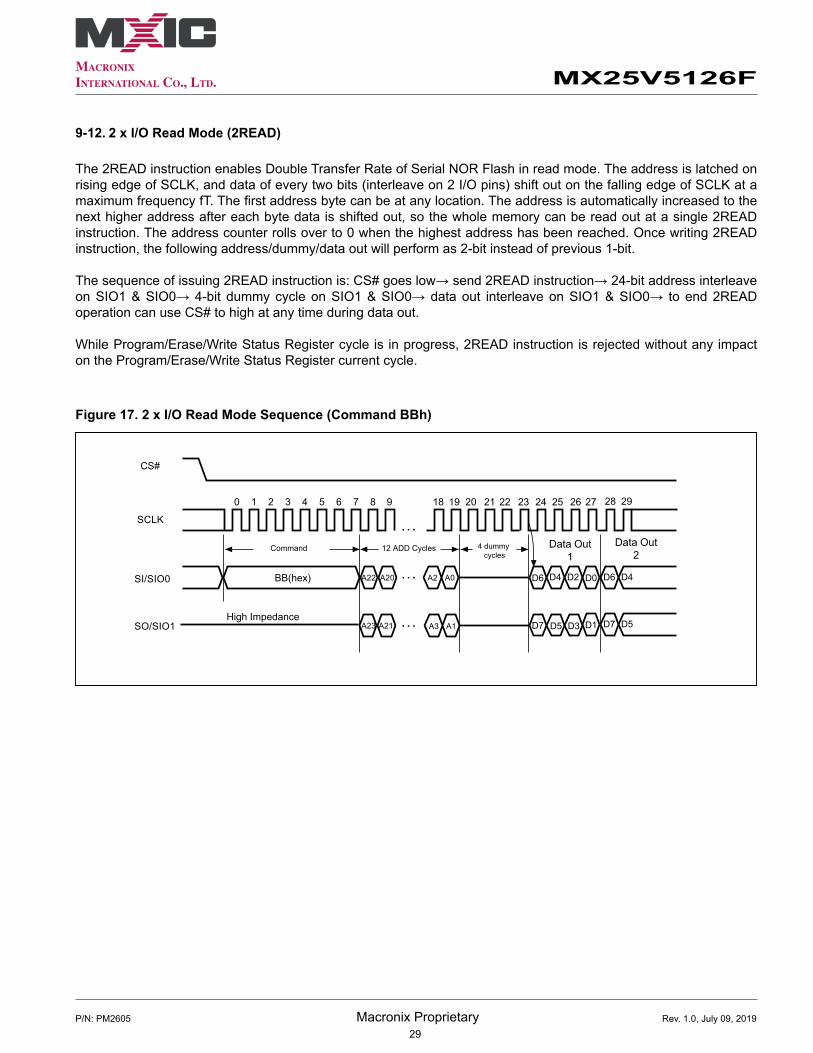
9-12. 2 x I/O Read Mode (2READ)
The 2READ instruction enables Double Transfer Rate of Serial NOR Flash in read mode. The address is latched on rising edge of SCLK, and data of every two bits (interleave on 2 I/O pins) shift out on the falling edge of SCLK at a maximumfrequencyfT.Thefirstaddressbytecanbeatanylocation.Theaddressisautomaticallyincreasedtothenext higher address after each byte data is shifted out, so the whole memory can be read out at a single 2READ instruction. The address counter rolls over to 0 when the highest address has been reached. Once writing 2READ instruction, the following address/dummy/data out will perform as 2-bit instead of previous 1-bit.
Thesequenceofissuing2READinstructionis:CS#goeslow→send2READinstruction→24-bitaddressinterleaveonSIO1&SIO0→4-bit dummycycleonSIO1&SIO0→dataout interleaveonSIO1&SIO0→ toend2READoperationcanuseCS#tohighatanytimeduringdataout.
While Program/Erase/Write Status Register cycle is in progress, 2READ instruction is rejected without any impact on the Program/Erase/Write Status Register current cycle.
Figure 17. 2 x I/O Read Mode Sequence (Command BBh)
High Impedance
21 3 4 5 6 7 80
SCLK
SI/SIO0
SO/SIO1
CS#
9 18 19 20
BB(hex)
21 22 23 24 25 26 27 28 29
D4
D5
D2
D3D7
D6 D6 D4D0
D7 D5D1
Command 12 ADD Cycles 4 dummy cycles
A22 A20 A2 A0
A3 A1A23 A21
…
…
…
Data Out1
Data Out2

30Rev. 1.0, July 09, 2019
MX25V5126F
P/N: PM2605 Macronix Proprietary
Figure 18. Sector Erase (SE) Sequence
21 3 4 5 6 7 8 9 29 30 310
23 22 2 1 0
MSB
SCLK
CS#
SI 20h
Command
Mode 3
Mode 024-Bit Address
9-13. Sector Erase (SE)
The Sector Erase (SE) instruction is for erasing the data of the chosen sector to be "1". The instruction is used for any 4K-byte sector. A Write Enable (WREN) instruction must execute to set the Write Enable Latch (WEL) bit before sending the Sector Erase (SE). Any address of the sector (Please refer to "Table2.MemoryOrganization") isavalidaddressforSectorErase(SE)instruction.TheCS#mustgohighexactlyatthebyteboundary(thelatesteighth of address byte been latched-in); otherwise, the instruction will be rejected and not executed.
Addressbits[Am-A12](Amisthemostsignificantaddress)selectthesectoraddress.
ThesequenceofissuingSEinstructionis:CS#goeslow→sendSEinstructioncode→3-byteaddressonSI→CS#goes high.
The SIO[1:0] are "don't care".
Theself-timedSectorEraseCycle time (tSE) is initiatedas soonasChipSelect (CS#)goeshigh.TheWrite inProgress (WIP) bit still can be checked during the Sector Erase cycle is in progress. The WIP sets 1 during the tSE timing, and sets 0 when Sector Erase Cycle is completed, and the Write Enable Latch (WEL) bit is reset. If the sector is protected by BP0-BP3 bits, the Sector Erase (SE) instruction will not be executed on the sector.

31Rev. 1.0, July 09, 2019
MX25V5126F
P/N: PM2605 Macronix Proprietary
9-14. Block Erase (BE32K)
The Block Erase (BE32K) instruction is for erasing the data of the chosen block to be "1". The instruction is used for 32K-byte block erase operation. A Write Enable (WREN) instruction must be executed to set the Write Enable Latch (WEL) bit before sending the Block Erase (BE32K). Any address of the block (Please refer to "Table 2.MemoryOrganization") isavalidaddressforBlockErase(BE32K) instruction. TheCS#mustgohighexactlyatthebyteboundary(the leastsignificantbitofaddressbytehasbeenlatched-in);otherwise, the instructionwillberejected and not executed.
ThesequenceofissuingBE32Kinstructionis:CS#goeslow→sendBE32Kinstructioncode→3-byteaddressonSI→CS#goeshigh.
The SIO[1:0] are don't care.
Theself-timedBlockEraseCycletime(tBE32K)isinitiatedassoonasChipSelect(CS#)goeshigh.TheWriteinProgress (WIP) bit still can be checked while the Block Erase cycle is in progress. The WIP sets during the tBE32K timing, and clears when Block Erase Cycle is completed, and the Write Enable Latch (WEL) bit is cleared. If the block is protected by BP0-BP3 bits, the array data will be protected (no change) and the WEL bit still be reset.
Figure 19. Block Erase 32KB (BE32K) Sequence (Command 52h)
24 Bit Address
21 3 4 5 6 7 8 9 29 30 310
23 22 2 01
MSB
SCLK
CS#
SI 52h
Command

32Rev. 1.0, July 09, 2019
MX25V5126F
P/N: PM2605 Macronix Proprietary
9-15. Block Erase (BE)
The Block Erase (BE) instruction is for erasing the data of the chosen block to be "1". The instruction is used for 64K-byte block erase operation. A Write Enable (WREN) instruction must execute to set the Write Enable Latch (WEL) bit before sending the Block Erase (BE). Any address of the block (Please refer to "Table2.MemoryOrganization") isavalidaddressforBlockErase(BE)instruction.TheCS#mustgohighexactlyatthebyteboundary(thelatesteighth of address byte been latched-in); otherwise, the instruction will be rejected and not executed.
ThesequenceofissuingBEinstructionis:CS#goeslow→sendBEinstructioncode→3-byteaddressonSI→CS#goes high.
The SIO[1:0] are "don't care".
The self-timedBlockEraseCycle time (tBE) is initiated as soon asChipSelect (CS#) goes high. TheWrite inProgress (WIP) bit still can be checked during the Block Erase cycle is in progress. The WIP sets 1 during the tBE timing, and sets 0 when Block Erase Cycle is completed, and the Write Enable Latch (WEL) bit is reset. If the block is protected by BP0-BP3 bits, the Block Erase (BE) instruction will not be executed on the block.
Figure 20. Block Erase (BE) Sequence
21 3 4 5 6 7 8 9 29 30 310
23 22 2 01
MSB
SCLK
CS#
SI D8h
Command
Mode 3
Mode 024-Bit Address

33Rev. 1.0, July 09, 2019
MX25V5126F
P/N: PM2605 Macronix Proprietary
9-16. Chip Erase (CE)
The Chip Erase (CE) instruction is for erasing the data of the whole chip to be "1". A Write Enable (WREN) instructionmustexecute toset theWriteEnableLatch (WEL)bitbeforesending theChipErase (CE).TheCS#must go high exactly at the byte boundary, otherwise the instruction will be rejected and not executed.
ThesequenceofissuingCEinstructionis:CS#goeslow→sendCEinstructioncode→CS#goeshigh.
The SIO[1:0] are "don't care".
The self-timedChip EraseCycle time (tCE) is initiated as soon asChip Select (CS#) goes high. TheWrite inProgress (WIP) bit still can be checked during the Chip Erase cycle is in progress. The WIP sets 1 during the tCE timing, and sets 0 when Chip Erase Cycle is completed, and the Write Enable Latch (WEL) bit is reset. If the chip is protected by BP0-BP3 bits, the Chip Erase (CE) instruction will not be executed. It will be only executed when BP0-BP3 bits are all set to "0" or BP3, BP2, BP1, BP0 are set to "1,X,0,0".
Figure 21. Chip Erase (CE) Sequence
21 3 4 5 6 70
60h or C7h
SCLK
SI
CS#
Command
Mode 3
Mode 0

34Rev. 1.0, July 09, 2019
MX25V5126F
P/N: PM2605 Macronix Proprietary
9-17. Page Program (PP)
The Page Program (PP) instruction is for programming memory bits to "0". One to 256 bytes can be sent to thedevice to be programmed. A Write Enable (WREN) instruction must be executed to set the Write Enable Latch (WEL)bit before sending the Page Program (PP). If more than 256 data bytes are sent to the device, only the last 256databyteswillbeacceptedandthepreviousdatabyteswillbedisregarded.ThePagePrograminstructionrequiresthatallthedatabytesfallwithinthesame256-bytepage.TheloworderaddressbyteA[7:0]specifiesthestartingaddress within the selected page. Bytes that will cross a page boundary will wrap to the beginning of the selectedpage. The device can accept (256 minus A[7:0]) data bytes without wrapping. If 256 data bytes are going to beprogrammed, A[7:0] should be set to 0.
ThesequenceofissuingPPinstructionis:CS#goeslow→sendPPinstructioncode→3-byteaddressonSI→atleast1-byteondataonSI→CS#goeshigh.
TheCS#mustbekeptlowduringthewholePageProgramcycle;TheCS#mustgohighexactlyatthebyteboundary(thelatest eighth bit of data being latched in), otherwise the instruction will be rejected and will not be executed.
Theself-timedPageProgramCycletime(tPP) is initiatedassoonasChipSelect(CS#)goeshigh.TheWrite inProgress (WIP) bit still can be checked during the Page Program cycle is in progress. The WIP sets 1 during the tPP timing, and sets 0 when Page Program Cycle is completed, and the Write Enable Latch (WEL) bit is reset. If the page is protected by BP0-BP3 bits, the Page Program (PP) instruction will not be executed.
The SIO[1:0] are "don't care".
Figure 22. Page Program (PP) Sequence
4241 43 44 45 46 47 48 49 50 52 53 54 5540
23
21 3 4 5 6 7 8 9 10 28 29 30 31 32 33 34 35
22 21 3 2 1 0
36 37 380
7 6 5 4 3 2 01
Data Byte 1
39
51
7 6 5 4 3 2 01
Data Byte 2
7 6 5 4 3 2 01
Data Byte 3 Data Byte 256
2079
2078
2077
2076
2075
2074
2073
7 6 5 4 3 2 01
2072
MSB MSB
MSB MSB MSB
SCLK
CS#
SI
SCLK
CS#
SI
02h
Command
Mode 3
Mode 024-Bit Address

35Rev. 1.0, July 09, 2019
MX25V5126F
P/N: PM2605 Macronix Proprietary
9-18. Deep Power-down (DP)
The Deep Power-down (DP) instruction places the device into a minimum power consumption state, Deep Power-downmode,inwhichthequiescentcurrentisreducedfromISB1toISB2.
ThesequenceofissuingDPinstruction:CS#goeslow→sendDPinstructioncode→CS#goeshigh.TheCS#mustgo high at the byte boundary (after exactly eighth bits of the instruction code have been latched-in); otherwise the instruction will not be executed. SIO[3:1] are "don't care".
AfterCS#goeshighthereisadelayoftDPbeforethedevicetransitionsfromStand-bymodetoDeepPowerdownmode and before the current reduces from ISB1 to ISB2. Once in Deep Power-down mode, all instructions will be ignored except Release from Deep Power-down (RDP).
The device exits Deep Power-down mode and returns to Stand-by mode if it receives a Release from Deep Power-down (RDP) instruction, power-cycle, or reset. Please refer to "Figure25.ReleasefromDeepPower-down(RDP)Sequence".
Figure 23. Deep Power-down (DP) Sequence (Command B9h)
21 3 4 5 6 70 tDP
Deep Power-down ModeStand-by Mode
SCLK
CS#
SI B9h
Command

36Rev. 1.0, July 09, 2019
MX25V5126F
P/N: PM2605 Macronix Proprietary
9-19. Release from Deep Power-down (RDP), Read Electronic Signature (RES)
TheReleasefromDeepPower-down(RDP)instructioniscompletedbydrivingChipSelect(CS#)High.WhenChipSelect(CS#) isdrivenHigh, thedevice isput in thestandbyPowermode.If thedevicewasnotpreviously intheDeep Power-down mode, the transition to the standby Power mode is immediate. If the device was previously in the DeepPower-downmode,though,thetransitiontothestandbyPowermodeisdelayedbytRES1,andChipSelect(CS#)must remain High for at least tRES1(max). Once in the standby mode, the device waits to be selected, so that it can receive, decode and execute instructions.
RES instruction is for reading out the old style of 8-bit Electronic Signature, whose values are shown as "Table4.IDDefinitions". This is not the same as RDID instruction. It is not recommended to use for new design. For new design, please use RDID instruction. Even in Deep power-down mode, the RDP and RES are also allowed to be executed, only except the device is in progress of program/erase/write cycles; there's no effect on the current program/erase/write cycles in progress.
The SIO[1:0] are don't care when during this mode.
TheRESinstructionisendedbyCS#goeshighaftertheIDbeenreadoutatleastonce.TheIDoutputsrepeatedlyifcontinuouslysendtheadditionalclockcyclesonSCLKwhileCS#isat low. If thedevicewasnotpreviously inDeep Power-down mode, the device transition to standby mode is immediate. If the device was previously in Deep Power-downmode, there's a delay of tRES2 to transit to standbymode, andCS#must remain to high at leasttRES2(max). Once in the standby mode, the device waits to be selected, so it can receive, decode, and execute instruction.
The RDP instruction is for releasing from Deep Power-down Mode.
Figure 24. Read Electronic Signature (RES) Sequence (Command ABh)
23
21 3 4 5 6 7 8 9 10 28 29 30 31 32 33 34 35
22 21 3 2 1 0
36 37 38
7 6 5 4 3 2 01High-Z
Electronic Signature Out
3 Dummy Bytes
0
MSB
Stand-by ModeDeep Power-down Mode
MSB
tRES2
SCLK
CS#
SI
SO
ABh
Command

37Rev. 1.0, July 09, 2019
MX25V5126F
P/N: PM2605 Macronix Proprietary
Figure 25. Release from Deep Power-down (RDP) Sequence
21 3 4 5 6 70 tRES1
Stand-by ModeDeep Power-down Mode
High-Z
SCLK
CS#
SI
SO
ABh
Command
Mode 3
Mode 0

38Rev. 1.0, July 09, 2019
MX25V5126F
P/N: PM2605 Macronix Proprietary
9-20. Software Reset - Reset-Enable (RSTEN) and Reset (RST)
The Software Reset operation combines two instructions: Reset-Enable (RSTEN) command and Reset (RST) command. It returns the device to standby mode. All the volatile bits and settings will be cleared then, which makes the device return to the default status as power on.
To executeReset command (RST), theReset-Enable (RSTEN) commandmust be executed first to perform theReset operation. If there is any other command to interrupt after the Reset-Enable command, the Reset-Enable will be invalid.
If the Reset command is executed during program or erase operation, the operation will be disabled, the data underprocessing could be damaged or lost.
The reset time is different depending on the last operation. Longer latency time is required to recover from aprogram operation than from other operations.
Figure 26. Software Reset Recovery
CS#
Mode
66 99
Stand-by Mode
tReady2

39Rev. 1.0, July 09, 2019
MX25V5126F
P/N: PM2605 Macronix Proprietary
10. POWER-ON STATE
The device is at the following states when power-up: - Standby mode (please note it is not deep power-down mode) - Write Enable Latch (WEL) bit is reset
The device must not be selected during power-up and power-down stage until the VCC reaches the following levels: - VCC minimum at power-up stage and then after a delay of tVSL - GND at power-downPleasenotethatapull-upresistoronCS#mayensureasafeandproperpower-up/downlevel.
An internal power-on reset (POR) circuit may protect the device from data corruption and inadvertent data change during power up state. When VCC is lower than VWI (POR threshold voltage value), the internal logic is reset and theflashdevicehasnoresponsetoanycommand.
For further protection on the device, if the VCC does not reach the VCC minimum level, the correct operation is not guaranteed. The write, erase, and program command should be sent after the below time delay: - tVSL after VCC reached VCC minimum level
The device can accept read command after VCC reached VCC minimum and a time delay of tVSL.Please refer to the "Figure34.Power-upTiming".
Notes: - To stabilize the VCC level, the VCC rail decoupled by a suitable capacitor close to package pins is
recommended. (generally around 0.1uF) - At power-down stage, the VCC drops below VWI level, all operations are disable and device has no response to
any command. The data corruption might occur during this stage if a write, program, erase cycle is in progress.

40Rev. 1.0, July 09, 2019
MX25V5126F
P/N: PM2605 Macronix Proprietary
ABSOLUTE MAXIMUM RATINGS
11. ELECTRICAL SPECIFICATIONS
CAPACITANCE TA = 25°C, f = 1.0 MHz
SYMBOL PARAMETER MIN. TYP. MAX. UNIT CONDITIONSCIN Input Capacitance 6 pF VIN = 0V
COUT Output Capacitance 8 pF VOUT = 0V
NOTICE:1. Stresses greater than those listed under ABSOLUTE MAXIMUM RATINGS may cause permanent damage
tothedevice. This isstressratingonlyandfunctionaloperationalsectionsof thisspecification isnot implied.Exposure to absolute maximum rating conditions for extended period may affect reliability.
2. Specificationscontainedwithinthefollowingtablesaresubjecttochange.3. Duringvoltagetransitions,allpinsmayovershoottoVCC+1.0VtoVCCor-0.5VtoGNDforperiodupto20ns.
RATING VALUEAmbient Operating Temperature -40°C to 85°C
Storage Temperature -65°C to 150°C
Applied Input Voltage -0.5VtoVCC+0.5V
Applied Output Voltage -0.5VtoVCC+0.5V
VCC to Ground Potential -0.5V to 4.0V
Figure 27. Maximum Negative Overshoot Waveform Figure 28. Maximum Positive Overshoot Waveform
0V
-1.0V
20ns
VCC+1.0V
VCC20ns

41Rev. 1.0, July 09, 2019
MX25V5126F
P/N: PM2605 Macronix Proprietary
DEVICE UNDER TEST
CL25K ohm
25K ohm+2.5V
CL=30pF or 15pF Including jig capacitance
Figure 29. DATA INPUT TEST WAVEFORMS AND MEASUREMENT LEVEL
ACMeasurement
Level
Input timing reference level Output timing reference level
0.8VCC0.7VCC
0.3VCC0.5VCC
0.2VCC
Note: Input pulse rise and fall time are <5ns
Figure 30. OUTPUT LOADING
Figure 31. SCLK TIMING DEFINITION
VIH (Min.)0.5VCC
VIL (Max.)
tCHCL
tCH
1/fSCLK
tCL
tCLCH

42Rev. 1.0, July 09, 2019
MX25V5126F
P/N: PM2605 Macronix Proprietary
Symbol Parameter Notes Min. Typ. Max. Units Test Conditions
ILI Input Load Current 1 ± 0.02 ± 2 uA VCC = VCC MaxVIN = VCC or GND
ILO Output Leakage Current 1 ± 0.02 ± 2 uA VCC = VCC MaxVOUT = VCC or GND
ISB1 VCC Standby Current 1 5 25 uA VIN = VCC or GNDCS#=VCC
ISB2 Deep Power-down Current 1 10 uA VIN = VCC or GND
CS#=VCC
ICC1 VCC Read 1 6 mAf=50MHz SCLK=0.1VCC/0.9VCC, SO=Open
ICC2 VCC Program Current (PP) 1 5 20 mA Program in Progress
CS#=VCC
ICC3VCC Write Status Register (WRSR) Current
2.1 15 mAProgram status register in progressCS#=VCC
ICC4 VCC Sector Erase Current (SE) 1 5 15 mA Erase in Progress
CS#=VCC
ICC5 VCC Chip Erase Current (CE) 1 5 20 mA Erase in Progress
CS#=VCC
VIL Input Low Voltage -0.5 0.3VCC VVIH Input High Voltage 0.7VCC VCC+0.4 VVOL Output Low Voltage 0.4 V IOL = 1.6mAVOH Output High Voltage VCC-0.2 V IOH = -100uA
VWI Low VCC Write Inhibit Voltage 3 1.5 2.1 V
Table 7. DC CHARACTERISTICS (Temperature = -40°C to 85°C for Industrial grade, VCC = 2.3V - 3.6V)
Notes :1.TypicalvaluesatVCC=2.5V,T=25°C.Thesecurrentsarevalidforallproductversions(packageandspeeds).2.Typicalvalueiscalculatedbysimulation.3.Not100%tested.
43Rev. 1.0, July 09, 2019
MX25V5126F
P/N: PM2605 Macronix Proprietary
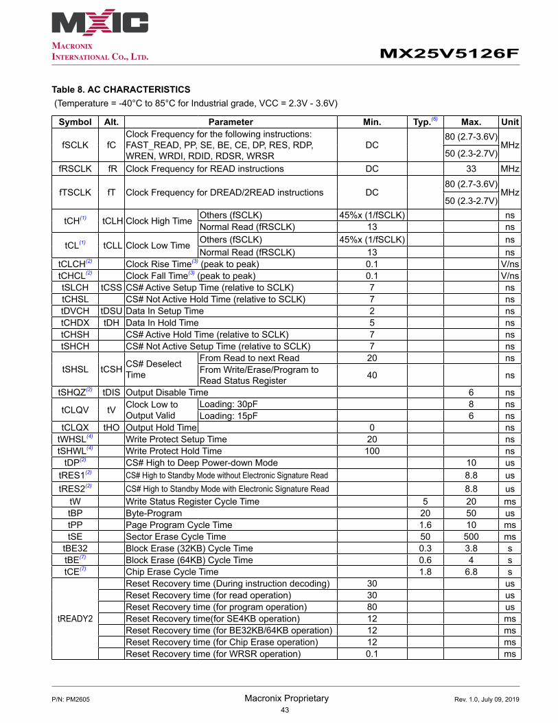
Table 8. AC CHARACTERISTICS (Temperature = -40°C to 85°C for Industrial grade, VCC = 2.3V - 3.6V)
Symbol Alt. Parameter Min. Typ.(6) Max. Unit
fSCLK fCClockFrequencyforthefollowinginstructions:FAST_READ, PP, SE, BE, CE, DP, RES, RDP,WREN, WRDI, RDID, RDSR, WRSR
DC80 (2.7-3.6V)
MHz50 (2.3-2.7V)
fRSCLK fR ClockFrequencyforREADinstructions DC 33 MHz
fTSCLK fT ClockFrequencyforDREAD/2READinstructions DC80 (2.7-3.6V)
MHz50 (2.3-2.7V)
tCH(1) tCLH Clock High Time Others (fSCLK) 45%x (1/fSCLK) nsNormal Read (fRSCLK) 13 ns
tCL(1) tCLL Clock Low Time Others (fSCLK) 45%x (1/fSCLK) nsNormal Read (fRSCLK) 13 ns
tCLCH(2) Clock Rise Time(3) (peak to peak) 0.1 V/nstCHCL(2) Clock Fall Time(3) (peak to peak) 0.1 V/nstSLCH tCSS CS#ActiveSetupTime(relativetoSCLK) 7 nstCHSL CS#NotActiveHoldTime(relativetoSCLK) 7 nstDVCH tDSU Data In Setup Time 2 nstCHDX tDH Data In Hold Time 5 nstCHSH CS#ActiveHoldTime(relativetoSCLK) 7 nstSHCH CS#NotActiveSetupTime(relativetoSCLK) 7 ns
tSHSL tCSH CS#DeselectTime
From Read to next Read 20 nsFrom Write/Erase/Program to Read Status Register 40 ns
tSHQZ(2) tDIS Output Disable Time 6 ns
tCLQV tV Clock Low to Output Valid
Loading: 30pF 8 nsLoading: 15pF 6 ns
tCLQX tHO Output Hold Time 0 nstWHSL(4) Write Protect Setup Time 20 nstSHWL(4) Write Protect Hold Time 100 ns
tDP(2) CS#HightoDeepPower-downMode 10 ustRES1(2) CS#HightoStandbyModewithoutElectronicSignatureRead 8.8 ustRES2(2) CS#HightoStandbyModewithElectronicSignatureRead 8.8 us
tW Write Status Register Cycle Time 5 20 mstBP Byte-Program 20 50 ustPP Page Program Cycle Time 1.6 10 mstSE Sector Erase Cycle Time 50 500 ms
tBE32 Block Erase (32KB) Cycle Time 0.3 3.8 stBE(7) Block Erase (64KB) Cycle Time 0.6 4 stCE(7) Chip Erase Cycle Time 1.8 6.8 s
tREADY2
Reset Recovery time (During instruction decoding) 30 usReset Recovery time (for read operation) 30 usReset Recovery time (for program operation) 80 usReset Recovery time(for SE4KB operation) 12 msReset Recovery time (for BE32KB/64KB operation) 12 msReset Recovery time (for Chip Erase operation) 12 msReset Recovery time (for WRSR operation) 0.1 ms

44Rev. 1.0, July 09, 2019
MX25V5126F
P/N: PM2605 Macronix Proprietary
Notes: 1.tCH+tCLmustbegreaterthanorequalto1/f(fCorfR).2.Valueguaranteedbycharacterization,not100%testedinproduction.3.Expressedasaslew-rate.4.OnlyapplicableasaconstraintforaWRSRinstructionwhenSRWDissetat1.5.Testcondition isshownas"Figure29.DATAINPUTTESTWAVEFORMSANDMEASUREMENTLEVEL"and"Figure30.OUTPUTLOADING".
6.TypicalvaluesgivenforTA=25°C.Not100%tested.7.The typicalspecificationof tBEand tCEcouldbeaccelerated to25msand50msrespectivelywhen the64KB
blockisblank(AllFFh).

45Rev. 1.0, July 09, 2019
MX25V5126F
P/N: PM2605 Macronix Proprietary
12. RECOMMENDED OPERATING CONDITIONS
At Device Power-Up and Power-Down
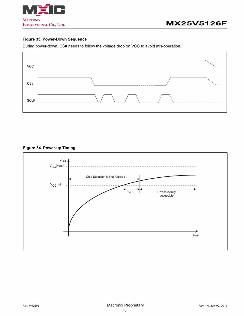
AC timing illustrated in "Figure32.ACTimingatDevicePower-Up" and "Figure33.Power-DownSequence" are for thesupplyvoltagesandthecontrolsignalsatdevicepower-upandpower-down.If thetiming inthefigures isignored, the device will not operate correctly.
Duringpower-upandpower-down,CS#needstofollowthevoltageappliedonVCCtokeepthedevicenottobeselected.TheCS#canbedrivenlowwhenVCCreachVcc(min.)andwaitaperiodoftVSL.
Notes :1.Sampled,not100%tested.2.ForACspectCHSL,tSLCH,tDVCH,tCHDX,tSHSL,tCHSH,tSHCH,tCHCL,tCLCHinthefigure,pleasereferto"Table8.ACCHARACTERISTICS".
Symbol Parameter Notes Min. Max. UnittVR VCC Rise Time 1 500000 us/V
Figure 32. AC Timing at Device Power-Up
SCLK
SI
CS#
VCC
MSB IN
SO
tDVCH
High Impedance
LSB IN
tSLCH
tCHDX
tCHCL
tCLCH
tSHCH
tSHSL
tCHSHtCHSL
tVR
VCC(min)
GND
46Rev. 1.0, July 09, 2019
MX25V5126F
P/N: PM2605 Macronix Proprietary
Figure 33. Power-Down Sequence
CS#
SCLK
VCC
Duringpower-down,CS#needstofollowthevoltagedroponVCCtoavoidmis-operation.
Figure 34. Power-up Timing
VCC
VCC(min)
Chip Selection is Not Allowed
tVSL
time
Device is fullyaccessible
VCC(max)

47Rev. 1.0, July 09, 2019
MX25V5126F
P/N: PM2605 Macronix Proprietary
12-1. Initial Delivery State
The device is delivered with the memory array erased: all bits are set to 1 (each byte contains FFh). The Status Register contains 00h (all Status Register bits are 0).
Figure 35. Power Up/Down and Voltage Drop
Table 9. Power-Up/Down Voltage and Timing
VCC
Time
VCC (max.)
VCC (min.)
V
tPWD
tVSL
Chip Select is not allowed
Full DeviceAccessAllowed
PWD (max.)
Note:Theseparametersarecharacterizedonly.
Symbol Parameter Min. Max. UnittVSL VCC(min.) to device operation 800 usVWI Write Inhibit Voltage 1.5 2.1 VVPWD VCC voltage needed to below VPWD for ensuring initialization will occur 0.9 V
tPWD The minimum duration for ensuring initialization will occur 300 us
When powering down the device, VCC must drop below VPWD for at least tPWD to ensure the device will initializecorrectly during power up. Please refer to "Figure35.PowerUp/DownandVoltageDrop" and "Table9.Power-Up/DownVoltageandTiming" below for more details.

48Rev. 1.0, July 09, 2019
MX25V5126F
P/N: PM2605 Macronix Proprietary
13. ERASE AND PROGRAMMING PERFORMANCE (2.3V - 3.6V)Parameter Min. Typ.(1) Max.(2) UnitWrite Status Register Cycle Time 5 20 msSector erase Time 50 500 msBlock erase Time (tBE32) 0.3 3.8 sBlock erase Time (tBE) 0.6(5) 4 sChip Erase Time 1.8(5) 6.8 sByte Program Time (via page program command) 20 50 usPage Program Time 1.6 10 msErase/Program Cycle 100,000 cyclesNotes: 1.Typicalprogramanderasetimeassumesthefollowingconditions:25°C,2.5V,andcheckerboardpattern.2.Underworstconditionsof85°Cand2.3V.3.System-level overhead is the time required to execute the first-bus-cycle sequence for the programming
command.4.Erase/ProgramcyclescomplywithJEDEC:JESD47&JESD22-A117standard.5.The typicalspecificationof tBEand tCEcouldbeaccelerated to25msand50msrespectivelywhen the64KB
blockisblank(AllFFh).
Notice:1.FactoryModemustbeoperatedin20°Cto45°CandVCC3.0V-3.6V.2.InFactorymode,theErase/Programoperationshouldnotexceed50cycles,and"ERASEANDPROGRAMMING
PERFORMANCE"100kcycleswillnotbeaffected.
14. ERASE AND PROGRAMMING PERFORMANCE (Factory Mode)Parameter Min. Typ.(1) Max.(2) UnitSector erase Time 20 msBlock erase Time (tBE32) 0.16 sBlock erase Time (tBE) 0.35 sChip Erase Time 0.6 sPage Program Time 1.3 msErase/Program Cycle 50 cycles
15. DATA RETENTION
Parameter Condition Min. Max. UnitData retention 55˚C 20 years
Min. Max.
Input Voltage with respect to GND on all power pins 1.5 VCCmaxInput Current on all non-power pins -100mA +100mATest conditions: VCC = VCCmax, one pin at a time (compliant to JEDEC JDESD78 standard).
16. LATCH-UP CHARACTERISTICS
49Rev. 1.0, July 09, 2019
MX25V5126F
P/N: PM2605 Macronix Proprietary
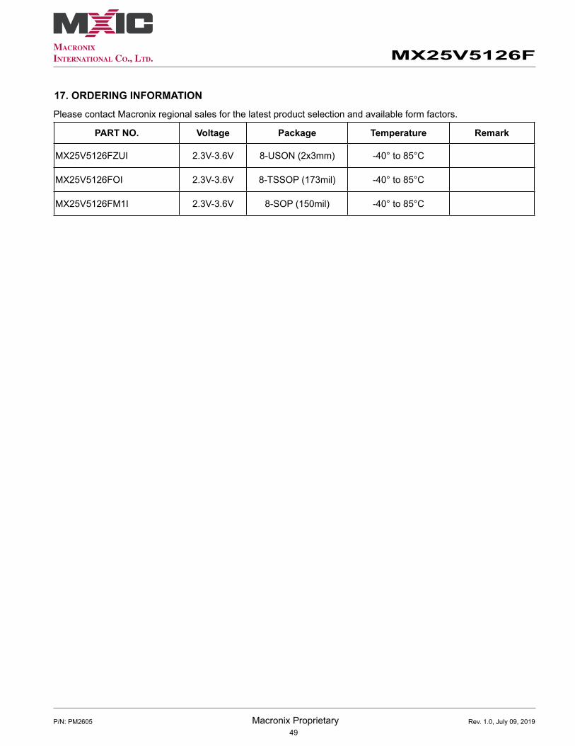
Please contact Macronix regional sales for the latest product selection and available form factors.
17. ORDERING INFORMATION
PART NO. Voltage Package Temperature Remark
MX25V5126FZUI 2.3V-3.6V 8-USON (2x3mm) -40° to 85°C
MX25V5126FOI 2.3V-3.6V 8-TSSOP (173mil) -40° to 85°C
MX25V5126FM1I 2.3V-3.6V 8-SOP (150mil) -40° to 85°C

50Rev. 1.0, July 09, 2019
MX25V5126F
P/N: PM2605 Macronix Proprietary
18. PART NAME DESCRIPTION
MX 25 V ZU I
TEMPERATURE RANGE:I: Industrial (-40°C to 85°C)
PACKAGE:ZU: 2x3mm 8-USONO: 173mil 8-TSSOPM1: 150mil 8-SOP
DENSITY & MODE:5126F: 512Kb
TYPE:V: 2.5V
DEVICE:25: Serial NOR Flash
5126F

51Rev. 1.0, July 09, 2019
MX25V5126F
P/N: PM2605 Macronix Proprietary
19. PACKAGE INFORMATION19-1. 8-USON (2x3mm)

52Rev. 1.0, July 09, 2019
MX25V5126F
P/N: PM2605 Macronix Proprietary
19-2. 8-pin TSSOP (173mil)

53Rev. 1.0, July 09, 2019
MX25V5126F
P/N: PM2605 Macronix Proprietary
19-3. 8-pin SOP (150mil)

54Rev. 1.0, July 09, 2019
MX25V5126F
P/N: PM2605 Macronix Proprietary
20. REVISION HISTORY Revision Descriptions Page
June 01, 20180.00 1. Initial Release. All
July 09, 20191.0 1. Removed "Advanced Information" to align with the product status. All
2. Revised "Figure17.2xI/OReadModeSequence(CommandBBh)". P293. Updated the title of Figure 29. P414. Revised LATCH-UP testing descriptions. P48

Except forcustomizedproductswhichhasbeenexpressly identified in theapplicableagreement,Macronix'sproducts are designed, developed, and/or manufactured for ordinary business, industrial, personal, and/or household applications only, and not for use in any applications which may, directly or indirectly, cause death, personal injury, or severe property damages. In the event Macronix products are used in contradicted to their targetusageabove,thebuyershalltakeanyandallactionstoensuresaidMacronix'sproductqualifiedforitsactual use in accordance with the applicable laws and regulations; and Macronix as well as it’s suppliers and/or distributors shall be released from any and all liability arisen therefrom.
Copyright© Macronix International Co., Ltd. 2018-2019. All rights reserved, including the trademarks and tradename thereof, such as Macronix, MXIC, MXIC Logo, MX Logo, Integrated Solutions Provider, Nbit, Macronix NBit, HybridNVM, HybridFlash, HybridXFlash, XtraROM, KH Logo, BE-SONOS, KSMC, Kingtech, MXSMIO, Macronix vEE, RichBook, Rich TV, OctaBus, FitCAM, ArmorFlash. The names and brands of third partyreferredthereto(ifany)areforidentificationpurposesonly.
For the contact and order information, please visit Macronix’s Web site at: http://www.macronix.com
MX25V5126F
55
MACRONIX INTERNATIONAL CO., LTD. reserves the right to change product and specifications without notice.