Embed Size (px)
Citation preview
Multiwalled Carbon Nanotube Growth Mechanism on Conductive and
Non-Conductive Barriers
Aun Shih Teh1,a, Daniel C.S. Bien1,b, Rahimah Mohd Saman1,c, Soo Kien Chen2,d, Kai Sin Tan1,e, Hing Wah Lee1,f
1MEMS and Nanotechnology, MIMOS Berhad, Technology Park Malaysia, 57000, Malaysia.
2Faculty of Science, University Putra Malaysia, 43400 Serdang, Malaysia
Keywords: Carbon nanotubes; Carbon materials; Chemical vapor deposition; Dielectrics
Abstract. We report on the catalytic growth of multiwalled carbon nanotubes by plasma enhanced
chemical vapor deposition using Ni and Co catalyst deposited on SiO2, Si3N4, ITO and TiNx barrier
layers; layers which are typically used as diffusive barriers of the catalyst material. Results revealed
higher growth rates on conductive ITO and TiNx as compared to non-conductive SiO2 and Si3N4
barriers. Micrograph images reveal the growth mechanism for nanotubes grown on SiO2, Si3N4 and
ITO to be tip growth while base growth was observed for the TiNx barrier layer. Initial conclusion
suggests that conductive diffusion barrier surfaces promotes growth rates however it is possible that
multiwalled carbon nanotubes grown on SiO2 and Si3N4 were encumbered as a result of the formation
of silicide as shown in the results here.
Introduction
Multiwalled carbon nanotubes (MWCNT) have vast potential applications in sensors [1,2],
interconnects [3], nanoelectromechanical devices [4] and electrochemical electrodes arrays [5] due to
its outstanding structural, mechanical and electrical properties. Integration of carbon nanotubes for
device applications can be achieved by ex-situ deposition such as spin/spray-on methods [6] or by
in-situ growth via catalytic chemical vapour deposition (CCVD) [7]. In the latter, nanotubes are
grown by decomposing a carbon-containing gas on catalyst deposited substrates. It has been
previously reported that nanotube growth will be inhibited by the formation of metal silicide if the
underlayer of the catalyst used is silicon [8]. The associated temperature where the catalyst material
diffuses into silicon and changes from pure metal to metal silicide, particularly for nickel (Ni) is
above 300oC. Due to silicidation, catalyst islands are not able to form after the annealing process.
Hence, a barrier layer such as silicon dioxide or titanium nitride is required.
As required by specific device applications, carbon nanotubes need to be grown on either
conductive or non-conductive/insulating type barriers. At present, these barrier layers are just used to
prevent silicide formation, hence a study comparing the growth rate and mechanisms on different
barrier types has not been reported, which is important to determine the suitable barrier type selection.
In this letter, the authors explore the growth of MWCNT on four typical barrier materials namely
silicon dioxide (SiO2), silicon nitride (Si3N4), indium tin oxide (ITO) and titanium nitride (TiNx).
These barrier layers are known to be compatible with CMOS process technology and are considered
as suitable barriers to prevent silicide formation of the catalyst material with silicon; that inhibits
nanotube growth.
Experimental and Results
The growth of MWCNT were performed by Plasma Enhanced Chemical Vapour Deposition
(PECVD) utilizing acetylene (C2H2) as the carbon feedstock while nickel (Ni) and cobalt (Co) were
chosen as the catalyst material. Ammonia (NH3) is added to C2H2 during the growth process to assist
Advanced Materials Research Vols. 403-408 (2012) pp 1201-1204Online available since 2011/Nov/29 at www.scientific.net© (2012) Trans Tech Publications, Switzerlanddoi:10.4028/www.scientific.net/AMR.403-408.1201
All rights reserved. No part of contents of this paper may be reproduced or transmitted in any form or by any means without the written permission of TTP,www.ttp.net. (ID: 132.177.228.65-25/02/13,12:48:17)
in the etching of by-products such as amorphous carbon. The SiO2 barriers was deposited by thermal
oxidation while the Si3N4, ITO, TiNx barriers and Ni, Co catalyst materials were deposited by
RF-magnetron sputtering with the deposition pressure maintained at 5x10⁻³
mbar for all layers.
Thicknesses of the barrier layers and catalyst material deposited are controlled at 20 nm and 4 nm
respectively. Prior to growth, the deposited catalyst material were annealed to nucleate the seeding
layer for the nanotube growth. Multiwalled carbon nanotubes were then grown on the annealed Ni and
Co catalyst layers with a C2H2:NH3 flow of ratio of 20:60 sccm at 700 oC.
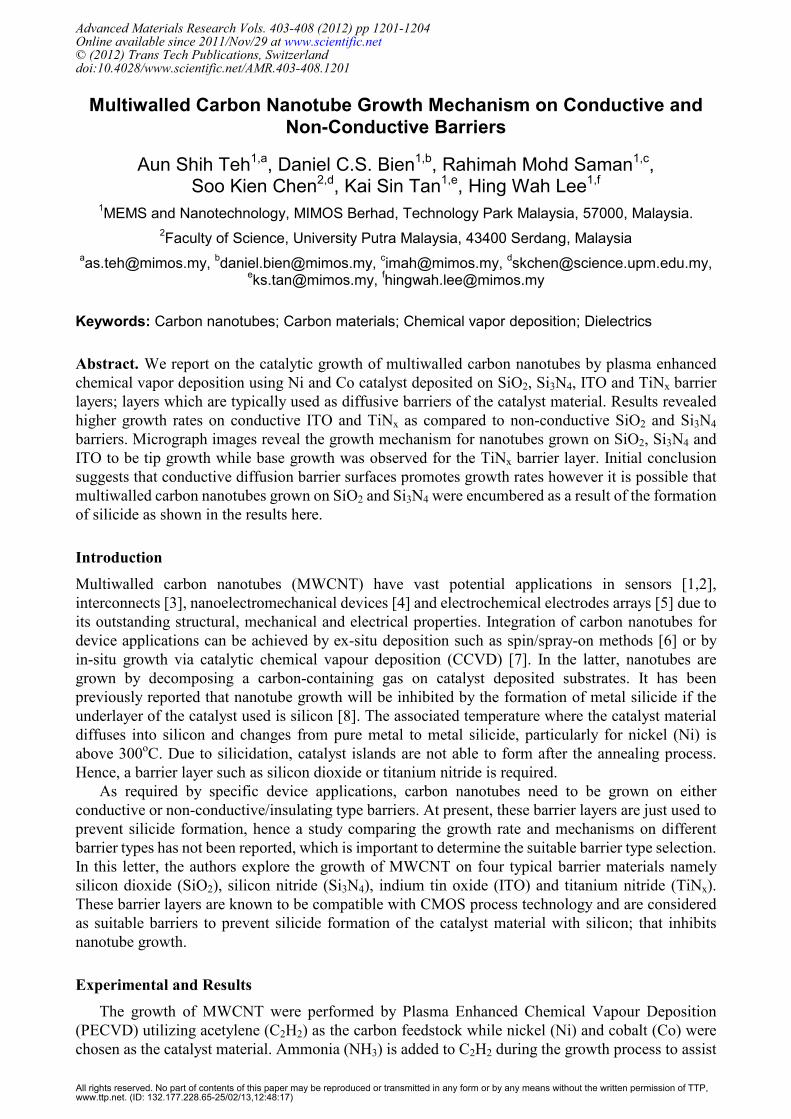
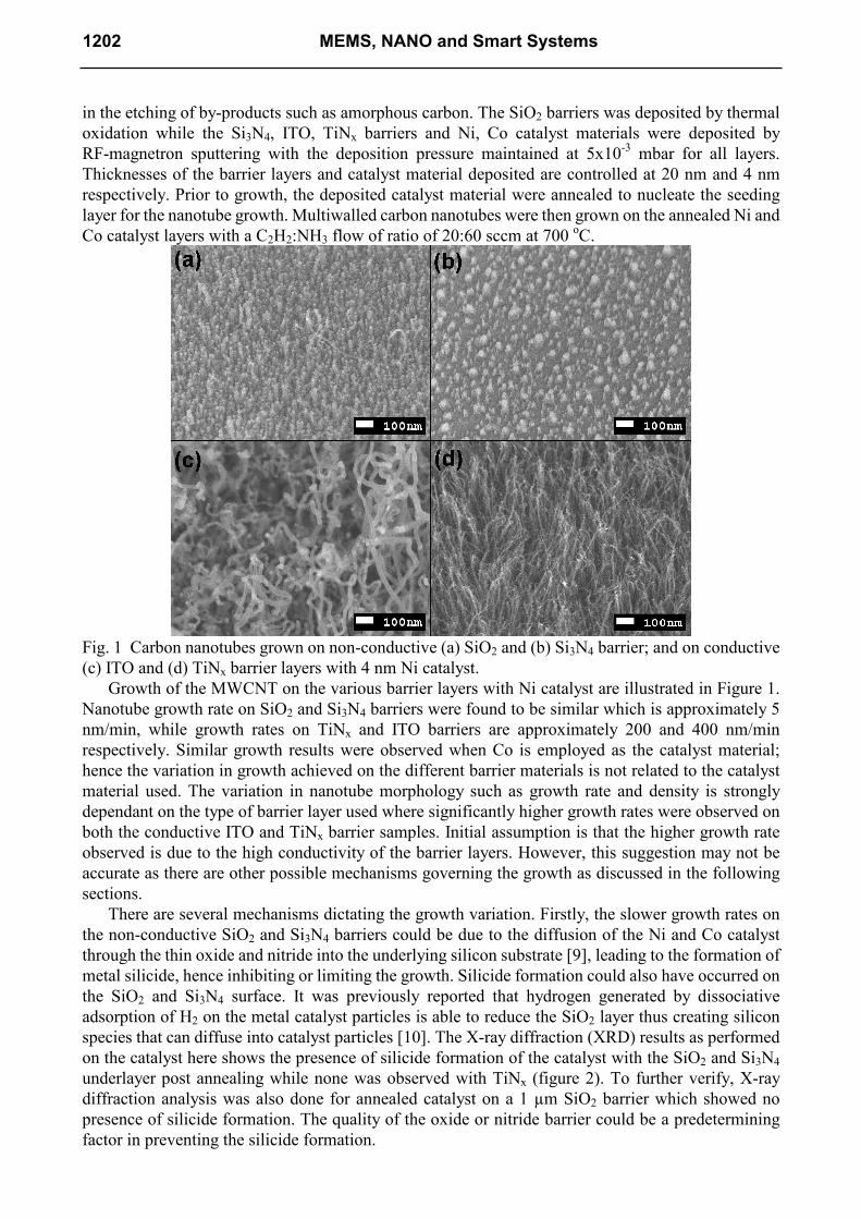
Fig. 1 Carbon nanotubes grown on non-conductive (a) SiO2 and (b) Si3N4 barrier; and on conductive
(c) ITO and (d) TiNx barrier layers with 4 nm Ni catalyst.
Growth of the MWCNT on the various barrier layers with Ni catalyst are illustrated in Figure 1.
Nanotube growth rate on SiO2 and Si3N4 barriers were found to be similar which is approximately 5
nm/min, while growth rates on TiNx and ITO barriers are approximately 200 and 400 nm/min
respectively. Similar growth results were observed when Co is employed as the catalyst material;
hence the variation in growth achieved on the different barrier materials is not related to the catalyst
material used. The variation in nanotube morphology such as growth rate and density is strongly
dependant on the type of barrier layer used where significantly higher growth rates were observed on
both the conductive ITO and TiNx barrier samples. Initial assumption is that the higher growth rate
observed is due to the high conductivity of the barrier layers. However, this suggestion may not be
accurate as there are other possible mechanisms governing the growth as discussed in the following
sections.
There are several mechanisms dictating the growth variation. Firstly, the slower growth rates on
the non-conductive SiO2 and Si3N4 barriers could be due to the diffusion of the Ni and Co catalyst
through the thin oxide and nitride into the underlying silicon substrate [9], leading to the formation of
metal silicide, hence inhibiting or limiting the growth. Silicide formation could also have occurred on
the SiO2 and Si3N4 surface. It was previously reported that hydrogen generated by dissociative
adsorption of H2 on the metal catalyst particles is able to reduce the SiO2 layer thus creating silicon
species that can diffuse into catalyst particles [10]. The X-ray diffraction (XRD) results as performed
on the catalyst here shows the presence of silicide formation of the catalyst with the SiO2 and Si3N4
underlayer post annealing while none was observed with TiNx (figure 2). To further verify, X-ray
diffraction analysis was also done for annealed catalyst on a 1 µm SiO2 barrier which showed no
presence of silicide formation. The quality of the oxide or nitride barrier could be a predetermining
factor in preventing the silicide formation.
1202 MEMS, NANO and Smart Systems
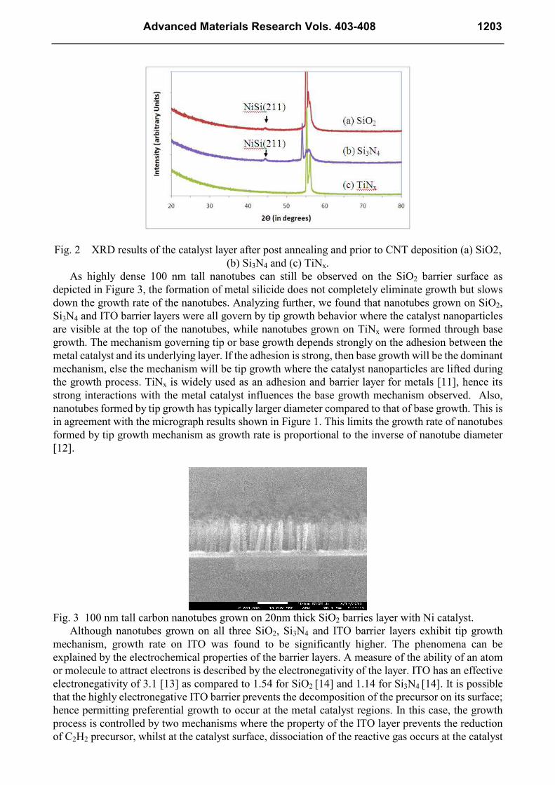
Fig. 2 XRD results of the catalyst layer after post annealing and prior to CNT deposition (a) SiO2,
(b) Si3N4 and (c) TiNx.
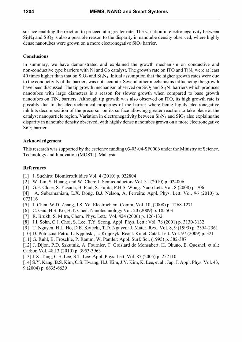
As highly dense 100 nm tall nanotubes can still be observed on the SiO2 barrier surface as
depicted in Figure 3, the formation of metal silicide does not completely eliminate growth but slows
down the growth rate of the nanotubes. Analyzing further, we found that nanotubes grown on SiO2,
Si3N4 and ITO barrier layers were all govern by tip growth behavior where the catalyst nanoparticles
are visible at the top of the nanotubes, while nanotubes grown on TiNx were formed through base
growth. The mechanism governing tip or base growth depends strongly on the adhesion between the
metal catalyst and its underlying layer. If the adhesion is strong, then base growth will be the dominant
mechanism, else the mechanism will be tip growth where the catalyst nanoparticles are lifted during
the growth process. TiNx is widely used as an adhesion and barrier layer for metals [11], hence its
strong interactions with the metal catalyst influences the base growth mechanism observed. Also,
nanotubes formed by tip growth has typically larger diameter compared to that of base growth. This is
in agreement with the micrograph results shown in Figure 1. This limits the growth rate of nanotubes
formed by tip growth mechanism as growth rate is proportional to the inverse of nanotube diameter
[12].
Fig. 3 100 nm tall carbon nanotubes grown on 20nm thick SiO2 barries layer with Ni catalyst.
Although nanotubes grown on all three SiO2, Si3N4 and ITO barrier layers exhibit tip growth
mechanism, growth rate on ITO was found to be significantly higher. The phenomena can be
explained by the electrochemical properties of the barrier layers. A measure of the ability of an atom
or molecule to attract electrons is described by the electronegativity of the layer. ITO has an effective
electronegativity of 3.1 [13] as compared to 1.54 for SiO2 [14] and 1.14 for Si3N4 [14]. It is possible
that the highly electronegative ITO barrier prevents the decomposition of the precursor on its surface;
hence permitting preferential growth to occur at the metal catalyst regions. In this case, the growth
process is controlled by two mechanisms where the property of the ITO layer prevents the reduction
of C2H2 precursor, whilst at the catalyst surface, dissociation of the reactive gas occurs at the catalyst
Advanced Materials Research Vols. 403-408 1203
surface enabling the reaction to proceed at a greater rate. The variation in electronegativity between
Si3N4 and SiO2 is also a possible reason to the disparity in nanotube density observed, where highly
dense nanotubes were grown on a more electronegative SiO2 barrier.
Conclusions
In summary, we have demonstrated and explained the growth mechanism on conductive and
non-conductive type barriers with Ni and Co catalyst. The growth rate on ITO and TiNx were at least
40 times higher than that on SiO2 and Si3N4. Initial assumption that the higher growth rates were due
to the conductivity of the barriers was not accurate. Several other mechanisms influencing the growth
have been discussed. The tip growth mechanism observed on SiO2 and Si3N4 barriers which produces
nanotubes with large diameters is a reason for slower growth when compared to base growth
nanotubes on TiNx barriers. Although tip growth was also observed on ITO, its high growth rate is
possibly due to the electrochemical properties of the barrier where being highly electronegative
inhibits decomposition of the precursor on its surface allowing greater reaction to take place at the
catalyst nanoparticle region. Variation in electronegativity between Si3N4 and SiO2 also explains the
disparity in nanotube density observed, with highly dense nanotubes grown on a more electronegative
SiO2 barrier.
Acknowledgement
This research was supported by the escience funding 03-03-04-SF0006 under the Ministry of Science,
Technology and Innovation (MOSTI), Malaysia.
References
[1] J. Suehiro: Biomicrofluidics Vol. 4 (2010) p. 022804
[2] W. Lin, S. Huang, and W. Chen: J. Semiconductors Vol. 31 (2010) p. 024006
[3] G.F. Close, S. Yasuda, B. Paul, S. Fujita, P.H.S. Wong: Nano Lett. Vol. 8 (2008) p. 706
[4] A. Subramaniam, L.X. Dong, B.J. Nelson, A. Ferreira: Appl. Phys. Lett. Vol. 96 (2010) p.
073116
[5] J. Chen, W.D. Zhang, J.S. Ye: Electrochem. Comm. Vol. 10, (2008) p. 1268-1271
[6] C. Gau, H.S. Ko, H.T. Chen: Nanotechnology Vol. 20 (2009) p. 185503
[7] R. Brukh, S. Mitra, Chem. Phys. Lett.: Vol. 424 (2006) p. 126-132
[8] J.I. Sohn, C.J. Choi, S. Lee, T.Y. Seong, Appl. Phys. Lett.: Vol. 78 (2001) p. 3130-3132
[9] T. Nguyen, H.L. Ho, D.E. Kotecki, T.D. Nguyen: J. Mater. Res., Vol. 8, 9 (1993) p. 2354-2361
[10] D. Potoczna-Petru, L. Kępiński, L. Krajczyk: React. Kinet. Catal. Lett. Vol. 97 (2009) p. 321
[11] G. Ruhl, B. Fröschle, P. Ramm, W. Pamler: Appl. Surf. Sci. (1995) p. 382-387
[12] J. Dijon, P.D. Szkutnik, A. Fournier, T. Goislard de Monsabert, H. Okuno, E. Quesnel, et al.:
Carbon Vol. 48,13 (2010) p. 3953-3963
[13] J.X. Tang, C.S. Lee, S.T. Lee: Appl. Phys. Lett. Vol. 87 (2005) p. 252110
[14] S.Y. Kang, B.S. Kim, C.S. Hwang, H.J. Kim, J.Y. Kim, K. Lee, et al.: Jap. J. Appl. Phys. Vol. 43,
9 (2004) p. 6635-6639
1204 MEMS, NANO and Smart Systems

MEMS, NANO and Smart Systems 10.4028/www.scientific.net/AMR.403-408 Multiwalled Carbon Nanotube Growth Mechanism on Conductive and Non-Conductive Barriers 10.4028/www.scientific.net/AMR.403-408.1201