Embed Size (px)
Citation preview

HAL Id: tel-01331314https://tel.archives-ouvertes.fr/tel-01331314
Submitted on 13 Jun 2016
HAL is a multi-disciplinary open accessarchive for the deposit and dissemination of sci-entific research documents, whether they are pub-lished or not. The documents may come fromteaching and research institutions in France orabroad, or from public or private research centers.
L’archive ouverte pluridisciplinaire HAL, estdestinée au dépôt et à la diffusion de documentsscientifiques de niveau recherche, publiés ou non,émanant des établissements d’enseignement et derecherche français ou étrangers, des laboratoirespublics ou privés.
Multispectral digital diffractive element for smartsunlight concentration for third generation photovoltaïc
devicesAbbas Kamal Hasan Albarazanchi
To cite this version:Abbas Kamal Hasan Albarazanchi. Multispectral digital diffractive element for smart sunlight con-centration for third generation photovoltaïc devices. Optics / Photonic. Université de Strasbourg,2015. English. �NNT : 2015STRAD029�. �tel-01331314�

Doctorale Mathématiques, Sciences de
l'Information et de l'Ingénieur
UDS-INSA -ICUBE
THÈSE
Présentée pour obtenir le grade de
Docteur de l’Université de Strasbourg Discipline : Sciences pour l’Ingénieur
Spécialité : Photonique
Par
ABBAS KAMAL HASAN ALBARAZANCHI
Composant diffractif numérique multispectral pour la concentration multifonctionnelle pour des
dispositifs photovoltaïques de troisième génération
Soutenue le 21 septembre 2015
Membres du jury :
Directeur de thèse : M. Patrick Meyrueis (EPR) Univ. de Strasbourg (Icube) Co-directeur de thèse : M. Pierre Ambs (Pr.) Univ. de Haute-Alsace (MIPS) Co-directeur de thèse : M. Philippe Gérard (Mcf.) INSA Strasbourg (Icube) Président du jury : M. Paul Montgomery (DR) CNRS Strasbourg (Icube) Rapporteur externe : M. Kevin Heggarty (Pr.) Telecom Bretagne Rapporteur externe : M. Michel Aillerie (Pr.) Univ. de Lorraine Examinateur : Examinateur :
M. Bruno Serio (Pr.) M. Dan Curticapean (Pr.)
Univ. de Paris Ouest Univ. d’Offenburg

Multispectral digital diffractive element for smart sunlight concentration for third generation photovoltaic devices
ABBAS KAMAL HASAN ALBARAZANCHI
21st September 2015

i
Acknowledgements
I would like to take this opportunity to express my appreciation and thanks for all the
persons that gave me the encouragement and support I need, to reach this point in my
academic career. I would like to thank my supervisors: principal advisor Patrick Meyrueis for
help me to learn the fundamental principles of the diffractive optical elements and for his
consistent guidance during the preparation of this doctoral thesis. I would also like to pay a
tribute for the effort and the very professional guidance of my co-advisor Prof. Pierre Ambs,
to bring out this thesis. I would like to express my great gratitude to Dr. Philippe Gerard for his
patience and his wise guidance through many comments and suggestions that helped me to
accomplish this doctoral work.
I would also like to thank all the members of photonics instrumentation and processes team;
especially, Dr. Sylvain Lecler, Dr. Patrice Twardowski, Dr. Pierre Pfeiffer, Dr. Manuel Flury, their
large experience and knowledge were very helpful for me on many occasions. I would also like to
give a warm thank to all the colleagues from the Icube-IPP team.
I would like to thank Prof. Kevin Heggarty from Telecom Bretagne for his assistance in fabricating
the diffractive optical element used in this work. I also very appreciate that he gave me the
opportunity to visit the clean room at Telecom Bretagne, to get an experimental experience about the
DOE’s fabrication. I would like also to give a special thanks to Giang-Nam Nguyen for his assistance
and the instructions he provide me during my stay in Telecom Bretagne in Brest for the fabrication of
the DOE's.
I thank my PhD committee: Dr. Paul Montgomery, Prof. Kevin Heggarty and Prof. Michel
Aillerie, Prof. Bruno Serio, and Prof. Dan Curticapean who provided me with their time and
attention to evaluate my work and provide me with insightful suggestions.
Finally and importantly, I dedicate very special thanks to my dear family, my wife and my
children’s Mohammed Hussein, Zahraa and Zainab. I would also like to thank my parents, whose
love and support through my whole life has given me the passion to pursue my education; to my
brothers and sisters, whose encouragement and support through all my life. I would like also to
express many thanks to my uncle Dr. Mehir for his help in preparation the draft of thesis. I would
not miss to thank all my friends for their support and encouragement during my doctoral thesis
work.

ii
Abstract Sunlight represents a good candidate for an abundant and clean source of renewable energy.
This environmentally friendly energy source can be exploited to provide an answer to the
increasing requirement of energy from the world. Several generations of photovoltaic cells
have been successively used to convert sunlight directly into electrical energy. Third
generation multijunction PV cells are characterized by the highest level of efficiency between
all types of PV cells. Optical devices have been used in solar cell systems such as optical
concentrators, optical splitters, and hybrid optical devices that achieve Spectrum Splitting and
Beam Concentration (SSBC) simultaneously. Recently, diffractive optical elements (DOE’s)
have attracted more attention for their smart use it in the design of optical devices for PV
cells applications.
This thesis was allocated to design a DOE that can achieve the SSBC functions for the
benefit of the lateral multijunction PV cells or similar. The desired design DOE's have a
subwavelength structure and operate in the far field to implement the target functions (i.e.
SSBC). Therefore, some modelling tools have been developed which can be used to simulate
the electromagnetic field behavior inside a specific DOE structure, in the range of
subwavelength features. Furthermore, a rigorous hybrid propagator is developed that is based
on both major diffraction theories (i.e. rigorous and scalar diffraction theory). The FDTD
method was used to model the propagation of the electromagnetic field in the near field, i.e.
inside and around a DOE, and the ASM method was used to model rigorously propagation in
the free space far field.
The proposed device required to implement the intended functions is based on two different
DOE’s components; a G-Fresnel (i.e. Grating and Fresnel lens), and an off-axis lens. The
proposed devices achieve the spectrum splitting for a Vis-NIR range of the solar spectrum
into two bands. These two bands can be absorbed and converted into electrical energy by two
different PV cells, which are laterally arranged. These devices are able to implement a low
concentration factor of “concentrator PV cell systems”. These devices also allow achieving
theoretically around 70 % of optical diffraction efficiency for the both separated bands. The
impact distance is very small for the devices proposed, which allows the possibility to
integrate these devices into compact solar cell systems. The experimental validation of the
fabricated prototype appears to provide a good matching of the experimental performance
with the theoretical model.

iii
Résumé
La lumière du soleil est un bon candidat comme source propre et abondante d'énergie
renouvelable. Cette source d'énergie écocompatible peut être exploitée pour répondre aux
besoins croissants en énergie du monde. Plusieurs générations de cellules photovoltaïques ont
été utilisées pour convertir directement la lumière solaire en énergie électrique. La troisième
génération de type multijonction des cellules photovoltaïques est caractérisée par un niveau
d'efficacité plus élevé que celui de tous les autres types de cellules photovoltaïques. Des
dispositifs optiques, tels que des concentrateurs optiques, des séparateurs optiques et des
dispositifs optiques réalisant simultanément la séparation du spectre et la concentration du
faisceau ont été utilisés dans des systèmes de cellules solaires. Récemment, les Eléments
Optiques Diffractifs (EOD) font l'objet d'un intérêt soutenu en vue de leur utilisation dans la
conception de systèmes optiques appliqués aux cellules photovoltaïques.
Cette thèse est consacrée à la conception d'un EOD qui peut réaliser simultanément la
séparation du spectre et la concentration du faisceau pour des cellules photovoltaïques de
type multijonction latéral ou similaire. Les EOD qui ont été conçus ont une structure sous-
longueur d'onde et fonctionnent en espace lointain pour implanter la double fonction
séparation du spectre et concentration du faisceau. Pour cette raison, des outils de simulation
ont été développés pour simuler le comportement du champ magnétique à l'intérieur de l'EOD
à structure sous-longueur d'onde. De plus, un propagateur hybride rigoureux a aussi été
développé, il est basé sur les deux théories de la diffraction, à savoir la théorie scalaire et la
théorie rigoureuse. La méthode FDTD (Finite Difference Time Domain) ou méthode de
différences finies dans le domaine temporel a été utilisée pour modéliser la propagation du
champ magnétique en champ proche c'est-à-dire à l'intérieur et autour de l'EOD. La méthode
ASM (Angular Spectrum Method) ou méthode à spectre angulaire a été utilisée pour
modéliser de façon rigoureuse la propagation libre en champ lointain.
Deux EOD différents ont été développés permettant d'implanter les fonctions souhaitées
(séparation du spectre et concentration du faisceau) ; il s'agit d'une part d'un composant
diffractif intitulé G-Fresnel (Grating and Fresnel lens) qui combine un réseau avec une
lentille de Fresnel et d'autre part d'une lentille hors-axe. Les composants proposés réalisent la
séparation du spectre en deux bandes pour une plage visible-proche infrarouge du spectre
solaire. Ces deux bandes peuvent être absorbées et converties en énergie électrique par deux
cellules photovoltaïques différentes et disposées latéralement par rapport à l'axe du système.

iv
Ces dispositifs permettent d'obtenir un faible facteur de concentration et une efficacité de
diffraction théorique d'environ 70 % pour les deux bandes séparées. Grâce à une distance de
focalisation faible, ces composants peuvent être intégrés dans des systèmes compacts de
cellules solaires. La validation expérimentale du prototype fabriqué montre une bonne
correspondance entre les performances expérimentales et le modèle théorique.

v
Résume de la thèse
INTRODUCTION GÉNÉRALE :
L’idée d’utiliser la lumière du soleil apparaît très prometteuse lorsqu’il s’agit d’obtenir une
source d’énergie propre et renouvelable. Une telle source d’énergie, favorable pour
l’environnement, peut être exploitée comme solution aux besoins croissants d’énergie dans le
monde. Parmi toutes les technologies de cellules photovoltaïques utilisées pour convertir directement l’énergie du soleil en électricité, on peut essentiellement distinguer plusieurs
générations. Les cellules photovoltaïques multijonctions, dites de troisième génération, sont celles qui présentent le plus haut rendement de conversion. Pour la réalisation d’une centrale
électrique à base de cellules solaires, il est nécessaire d’adjoindre à la cellule des systèmes
optiques tels que des concentrateurs, des séparateurs ou d’autres systèmes hybrides qui
remplissent simultanément les fonctions de séparation de longueur d’onde et de concentration
de faisceau. Depuis peu de temps, les Éléments Optiques Diffractifs (EODs) commencent à susciter un intérêt pour une application dans la conception de ces systèmes optiques qu’il faut
ajouter aux cellules photovoltaïques. Le but de cette thèse est de proposer une solution de système optique reposant sur l’utilisation d’un élément optique diffractif pour remplir simultanément les fonctions de séparation de longueur d’onde et de concentration de faisceau. Cette solution sera destinée aux cellules solaires multijonctions. De façon générale, les EODs sont des candidats prometteurs pour remplir les fonctions de gestion du rayonnement solaire dans les systèmes photovoltaïques. Les EODs ont théoriquement la capacité, avec des méthodes de conception optimales, de contrôler sur un spectre large la propagation de ce rayonnement solaire. Les dispositifs optiques conçus à partir d’EODs peuvent être utilisés pour augmenter le
rendement de cellules photovoltaïques. Les EODs sont obtenus en changeant localement soit l’épaisseur ou l’indice de réfraction
d’une surface à l’échelle du micromètre. Ainsi, lorsque cette surface est éclairée par un faisceau lumineux, cela permet de générer localement des déphasages sur cette onde incidente. L’interférence des ondes ayant subi ce déphasage local permet ensuite d’obtenir à
une distance donnée un faisceau pouvant présenter presque toute type de distribution spatiale d’intensité. L’application de ces EODs concerne donc la mise en forme d’un faisceau pour
obtenir le motif de distribution d’intensité souhaité dans le plan dit de reconstruction de
l’élément. Les EODs permettent donc la miniaturisation de systèmes optiques grâce à leur planéité et leur très faible épaisseur. Les progrès de la photolithographie permettent de réaliser des EODs avec une taille critique (pixel: plus petit élément constituant la forme à donner à la modulation de surface) plus petite que la longueur d’onde. De plus les progrès dans la réalisation des éléments dit maîtres et dans les techniques de réplication réduisent considérablement le coût associé à une production de masse de ces éléments. Les systèmes de production d’énergie solaire qui consistent en l’intégration d’une cellule
solaire photovoltaïque multijonction avec un EOD représentent une solution intéressante. Ces
systèmes compacts de cellules photovoltaïques peuvent être utilisées pour récupérer l’énergie
du soleil avec l’avantage d’un haut rendement de conversion.

vi
CH. I. CELLULES PHOTOVOLTAÏQUES, TECHNOLOGIES ET SYSTÈMES
Dans un système photovoltaïque de production d’énergie solaire, la lumière du soleil est
convertie en électricité grâce à l’effect photovoltaïque. Les dispositifs photovoltaïques sont
généralement réalisés à l’aide de matériaux semiconducteurs. Par conséquent, quand des photons d’énergie supérieure à la bande interdite du matériau semiconducteur frappent le
dispositif, une paire électron-trou peut être créée dans les quasi niveaux de Fermi grâce à la transition des électrons d’un bas vers un haut niveau d’énergie, comme montré sur la figure
(1.1).
Figure 1.1 : illustration de l’effet photovoltaïque
En général, le rendement d’une cellule photovoltaïque dépend de plusieurs limitations en
fonction du type de cellule. La limite de Shockley-Queisser fait référence à l’efficacité
maximale théorique d’une cellule photovoltaïque utilisant une jonction p-n. Cette limite est calculée en regardant l’énergie qui est extraite par photon provenant de la lumière du soleil.
Les cellules faites à partir d’une seule jonction p-n ne peuvent pas convertir tout le flux de photons du soleil en énergie électrique. Les cellules solaires de première génération sont celles qui nécessitent le plus de matériau semiconducteur et sont donc les plus chères. Les cellules de seconde génération utilisent la technologie des couches minces ce qui réduit leur coût. Cependant un fort piégeage est nécessaire particulièrement pour les grandes longueurs d’onde. C’est là une limitation de cellules de seconde génération. Celles de troisième génération éliminent les pertes par thermalisation en utilisant plusieurs niveaux d’énergie pour les bandes interdites. Il est ainsi possible d’obtenir un rendement élevé. Le coût de cette technologie reste cependant élevé. Traditionnellement, les cellules solaires de volume qui sont généralement fabriquées à partir de wafers de silicium mono cristallin sont celles qui sont les plus utilisées. Le problème fondamental avec ce genre de dispositif est la thermalisation des électrons (et des trous), phénomène par lequel les photons d’énergie élevée dissipent leur excès d’énergie en chaleur. Les cellules en tandem ont été proposées comme solution à cette limitation de Shockley-Queisser. Dans ce scénario, deux ou plusieurs jonctions avec des bandes interdites différentes sont reliées en série comme présenté sur la figure (1.2) où la première partie du rayonnement incident est absorbée du côté du dispositif ayant la plus large bande. Actuellement, le

vii
rendement maximal de conversion des cellules solaires mesuré dans le monde est de 44.7 % pour une cellule solaire en tandem.
Figure 1.2 : Illustration d’une cellule multi-jonctions.
On distingue deux types de systèmes à base de cellules photovoltaïques : les planaires et les non planaires. La majorité des systèmes en production aujourd’hui sont de type planaire.
Généralement, il n’y a pas de système optique placé avant les cellules photovoltaïques elles-mêmes à l’exception d’une couverture de protection. Pour les systèmes non planaires, un
dispositif optique peut être intégré avec la cellule pour former un seul système. Ces dispositifs optiques sont utilisés pour réduire significativement le prix de revient de l’énergie
produite. La grande surface de conversion de cellules chères est remplacée par un système optique moins cher qui permet d’augmenter les performances du système solaire complet. En général, les systèmes non planaires peuvent être classés en trois catégories en fonction du type de dispositif optique qui est ajouté aux cellules photovoltaïques : les systèmes de cellules photovoltaïques à concentrateur, ceux à séparateur de longueur d’onde et les
systèmes hybrides remplissant simultanément les deux fonctions de séparation de longueur d’onde et de concentration de faisceau. La fabrication de cellules solaires multiples montées
en tandem est chère et le procédé de fabrication peut causer une pollution importante de l’environnement. Les systèmes non planaires présentent plusieurs avantages comparés aux systèmes planaires à une seule jonction. D’abord le rendement de production d’énergie
électrique est supérieur. Ensuite, ils nécessitent l’utilisation de moins de matériau
semiconducteur ce qui contribue non seulement à réduire le coût mais aussi à diminuer la pollution associée au procédé de fabrication. Enfin, le système présente un meilleur rendement pour les zones chaudes et ensoleillées. Le principe de fonctionnement des cellules photovoltaïque de troisième génération repose sur l’utilisation de plusieurs cellules ayant des valeurs de bandes interdites différentes. En
conséquence, la conversion de la totalité du spectre solaire peut être obtenue ce qui conduit à une augmentation du rendement des systèmes solaires. Les cellules de troisième génération peuvent être classées en deux catégories en fonction de la méthode utilisées pour placer les différentes jonctions des cellules.
i. Systèmes de cellules solaires placées verticalement
Dans ce type de cellule, les différentes jonctions des cellules sont empilées verticalement pour forme un seul système. Chaque jonction peut convertir une partion du spectre solaire ayant une énergie supérieure à sa bande interdite. La bande interdite de chaque jonction

viii
décroit du haut vers le bas. Ce type de cellule de troisième génération présente certains inconvénients dus à la complexité du procédé de fabrication et ces cellules sont aussi chères.
ii. Systèmes de cellules solaires placées latéralement
Une solution alternative pour les cellules de troisième génération est proposée pour surmonter les restrictions imposées par le procédé de fabrication des cellules verticales. Cette fois, les différentes jonctions des différentes cellules sont arrangées en parallèle pour former un seul système de cellule photovoltaïque. Le spectre du soleil est séparé par le système de séparation de longueurs d’onde pour être orienté vers chaque cellule. Cette solution offre la
meilleure flexibilité pour le procédé de fabrication des cellules de troisième génération. Chaque cellule peut être fabriquée indépendamment et peut être placée ensuite sur une surface place, ce qui aussi permet d’augmenter le nombre de jonction photovoltaïques dans
un système solaire. La figure (1.3) illustre la méthode de collecte du spectre solaire pour les deux types de cellules de troisième génération. Le système de cellules photovoltaïques à arrangement latéral permet d’atteindre des hauts rendements de production électrique lorsque couplé à un système approprié de séparation de longueurs d’onde.
-a-
-b-
Figure 1.3 : Méthodes de récupération du spectre solaire à l’aide de cellules de troisième génération.
a- Systèmes de cellules placées verticalement. b- Systèmes de cellules placées latéralement.
Les systèmes hybrides de cellules photovoltaïques qui peuvent réaliser la séparation des longueurs d’onde et la concentration du faisceau ont été proposées pour les cellules multijonction à arrangement latéral de façon à réduire les coûts de fabrication et d’augmenter
le rendement. Ce système hybride qui comporte des éléments optiques diffractifs représente le dispositif idéal présentant un rendement de conversion élevé à un coût raisonnable. Les EOD peuvent réaliser un bon contrôle et une bonne gestion de la lumière solaire incidente pour de larges bandes de longueurs d’onde. De plus, les EOD peuvent être fabriqués à partir de matériaux légers et bon marché. Ils peuvent être utilisés sur de grandes surfaces et sur une faible épaisseur, ce qui permet de réaliser des systèmes compacts de cellules photovoltaïques. CH.II. MODELISATION ET MÉTHODES DE CONCEPTION POUR LES ÉLÉMENTS OPTIQUES DIFFRACTIFS
Les Éléments Optiques Diffractifs (EOD) sont des dispositifs optiques se présentant sous la forme d’une surface planaire ayant subi une microstructuration. Ces motifs micrométriques contrôlent la propagation de la lumière en utilisant le mécanisme de la diffraction. On
ix
observe un intérêt croissant de la communauté des opticiens pour les EOD, cela à cause de trois raisons principales. Premièrement, les EOD jouent un rôle important dans un nombre croissant d’applications de l’optique moderne. On en trouve des applications dans la micro-optique, la nano-optique, l’optique intégrée et les micros systèmes électriques optiques et mécaniques (MEOMS). Deuxièmement, les progrès dans les moyens de calculs permettent de concevoir et de simuler les performances d’EOD complexes et cela avec une grande exactitude. Troisièmement, les progrès dans les micros et nano technologies permettent de réaliser des EOD à partir de matériaux légers et peu coûteux même pour des tailles critiques de pixels faibles. En conséquence, des systèmes optiques compacts peuvent être fabriqués à partir d’EOD en présentant une miniaturisation plus élevées que les systèmes optiques
conventionnels.
Théories de la diffraction généralement utilisées pour des éléments optiques diffractifs
La nature électromagnétique de la lumière sera utilisée pour expliquer le phénomène de diffraction que l’on rencontre lorsque la lumière se propage à travers un EOD. La nature électromagnétique de la lumière est décrite à l’aide des équations de Maxwell. On trouve
généralement dans la littérature deux modèles: la théorie scalaire de diffraction et la théorie rigoureuse de la diffraction. La différence principale entre ces deux approches réside dans la façon où l’on résout les équations de Maxwell. Avec la théorie scalaire, on ne traite que d’une
seule composante associée soit au champ électrique soit au champ magnétique. Avec la théorie rigoureuse, les équations de Maxwell sont résolues sans aucune approximation et cela permet de prendre en compte toutes les interactions entre toutes les composantes des champs électrique et magnétique.
1.Théorie scalaire de la diffraction
Cette approximation donne de bons résultats lorsqu’il s’agit d’EOD présentant un profil
d’épaisseur peu épais. Dans ce cas, pour deux rayons de lumière qui traversent l’élément en
des endroits différents tout se passe comme si ils subissaient uniquement un retard lié à la différence de chemin optique et continuaient leur trajet à l’intérieur de l’EOD sans être
déviés. Cette approximation nécessite que la modulation d’épaisseur de la surface de
l’élément soit inférieure à la longueur d’onde de la lumière qui l’éclaire. La théorie scalaire de la diffraction repose ainsi sur l’approximation dite des éléments
minces. Cette dernière approximation permet d’écrire la composante scalaire U0 du champ
diffracté à la sortie de l’élément comme la simple multiplication de la même composante de ce champ à l’entrée de avec la fonction de transparence de l’élément. Cela est présenté sur la
figure (2.1). La composante complexe U de ce même champ diffracté calculée sur un plan de reconstruction, après propagation de l’onde dans l’espace libre, peut être obtenue en résolvant
l’équation de Helmholtz. La théorie scalaire de la diffraction implique la conversion de
l’équation de Helmholtz qui est une équation aux dérivées partielles en une équation intégrale
en utilisant le théorème de Green. Diverses formulations de la diffraction assez utilisées dérivent de l’équation de Helmholtz, ce sont la formulation de Rayleigh-Sommerfeld (RS), celle de Fresnel-Kirchhoff (FK) et la méthode du spectre des ondes planes (ASM). Deux autres approximations font suite à RS ce sont les formulations de Fresnel et de Fraunhofer. Ces dernières présentent l’avantage de faire appel à des transformées de Fourier.

x
Figure 2.1 : Schéma typique pour la description de la propagation de la lumière dans le cadre de l’approximation scalaire de la diffraction.
2. Théorie rigoureuse de la diffraction
Les équations de Maxwell sont résolues sans aucune approximation afin d’obtenir la nature
exacte de l’interaction entre le champ d’excitation et la structure diffractante. Les interactions mutuelles des champs électriques et magnétiques qui ont lieu dans l’élément ont des
conséquences directes sur la champ observé sur le plan de reconstruction. Plusieurs méthodes numériques différentes sont utilisées. En général, ces méthodes peuvent être regroupées en deux grandes catégories en fonction des formes prises par les équations de Maxwell. À savoir, les formes intégrale et différentielle. On distingue essentiellement quatre approches:
I. La méthode des éléments de frontière (BEM) est particulièrement adaptée pour l’étude
d’EOD de dimension finie car elle n’est pas limités à des structures périodiques. II. La méthode des éléments finies (FEM) est assez proche de la BEM. Cette méthode est
souvent utilisée dans le domaine des micro-ondes pour analyser des problèmes de diffusion et de guides d’ondes.
III. La méthode rigoureuse des ondes couplées (RCWA) est très utilisée pour calculer les efficacités de diffraction de réseaux de diffraction ou d’EOD périodiques. La RCWA
utilise la forme différentielle des équations de Maxwell. IV. La méthode des différences finies à dépendance temporelle (FDTD) est certainement
la méthode la plus connue pour la résolution de problèmes en électrodynamique. Elle peut être utilisée pour résoudre tous les problèmes de rayonnement électromagnétique, pour tous types de matériaux et de formes.
3. Théorie du milieu effectif
La théorie du milieu effectif (EMT) est utilisée pour décrire l’interaction entre un faisceau
lumineux incident et une structure de période sub-longueur (SWS). Il s’agit d’une
formulation analytique décrivant l’équivalence entre un milieu inhomogène présentant une modulation de surface de période sub-longueur d’onde et un milieu homogène de type couche
mince.

xi
Figure 2.2: Interface entre deux matériaux avec réseau de diffraction sub-longueur d’onde et
son matériau homogène effectif.
L’indice de réfraction effectif est défini à l’aide du vecteur d’onde de l’ordre zéro se
propageant dans la structure. Les coefficients de réflexion, de transmission en intensité ainsi que le déphasage introduit par la structure sub-longueur d’onde peuvent calculés en utilisant la théorie des couches minces optiques. Prenant en compte le fait que le nombre d’onde β est généralement fonction de la fréquence, il en sera de même pour l’indice de réfraction effectif.
De plus β dépend aussi de l’état de polarisation de l’onde, ainsi une structure de période sub-longueur d’onde sera anisotrope. Les EOD sont des dispositifs optiques capable de réaliser plusieurs fonctions qui ne peuvent être obtenues à l’aide de composants optiques conventionnels. Les EOD présentent des caractéristiques remarquables en regard des fonctions qu’ils réalisent et des moyens de
fabrication nécessaires à leur réalisation. Les EOD peuvent remplir plusieurs fonctions telles que la mise en forme, la séparation, la combinaison, la concentration de faisceau, etc. ... qui peuvent être utilisées dans de nombreuses applications.
CH. III. MODÉLISATION D’ÉLÉMENTS OPTIQUES DIFFRACTIFS:
Nous proposons un propagateur hybride qui utilise principalement la méthode des différences finies à dépendance temporelle (FDTD), comme exemple d’approche rigoureuse,
et la méthode du spectre des ondes planes (ASM), comme exemple d’approche scalaire.
L’utilisation du propagateur hybride (FDTD-ASM) offre la possibilité de modéliser et de concevoir des EOD de grande taille qui reconstruisent leur champ à grande distance. Le propagateur hybride (FDTD-ASM) que nous proposons est mis en œuvre en deux étapes
comme présenté figure (3.1), elles sont les suivantes:
I. La méthode FDTD est utilisée pour simuler la propagation de la lumière dans l’épaisseur de l’EOD et quelques micromètres au delà. Dès que la méthode
FDTD obtient le champ permanent établi, les composantes du champ électromagnétique sont préparées en vue de leur utilisation par la méthode ASM.
II. L’ASM est utilisée pour réaliser la propagation dans l’espace libre de la
lumière. Les composantes du champs électromagnétiques issues de la FDTD sont rééchantillonnées pour respecter les conditions d’échantillonnage demandées par l’ASM. L’ASM, présentée dans le cadre de l’approximation scalaire, est complétée par deux autres équations utilisant la nature vectorielle des ondes planes et qui permettent d’obtenir les autres composantes des champs
électrique et magnétique. On distingue en cela les polarisations TE et TM. En

xii
conséquence, le vecteur de Poynting et les efficacités de diffraction sont calculées rigoureusement.
-a-
-b-
Figure 3.1: Illustration du propagateur hybride FDTD-ASM. a- Domaine de calcul de la FDTD. b- Domaine de calcul de l’ASM.
Toutes les simulations FDTD ont été obtenues en utilisant le logiciel Meep développé au MIT. Les simulations ASM ont utilisé un code Matlab que nous avons développé. L’application de ce principe de simulation hybride FDTD -ASM est présentée figure (3.2) dans le cas d’une lentille diffractive.
Figure 3.2 : Principe de la simulation avec le propagateur hybride FDTD-ASM. a- Distribution du champ électrique par la FDTD dans et à proximité de la lentille.
b- Calcul du vecteur de Poynting obtenu par la méthode ASM. Éléments Optiques Diffractifs utilisant des Structures sub-longueur d’onde
Les EOD réalisée par une modulation d’épaisseur de leur surface à l’échelle sub-longueur d’onde ont l’avantage de présenter des comportements intéressants. Ces caractéristiques ne peuvent pas être obtenues à l’aide d’EOD multi-niveaux classiques. La caractéristique la plus remarquable est une efficacité de diffraction élevée dans l’ordre zéro. La théorie
électromagnétique rigoureuse est utilisée pour obtenir la correspondance entre l’indice de
réfraction effectif et le taux de remplissage du réseau. Dans notre étude nous utilisons pour cela la méthode FDTD. Nous évaluons alors le déphasage introduit par un réseau de diffraction de période sub-longueur d’onde (utilisation de conditions aux limites périodiques) comme montré sur la figure (3.3).

xiii
Figure 3.3 : Schéma d’un période 1D d’un réseau de diffraction à période sub-longueur d’onde.
Le domaine de calcul pour la FDTD consiste en un pilier de largeur et de hauteur placé à l’intérieur de la période du réseau. Le déphasage est calculé en variant la largeur
du pilier à l’intérieur de ce domaine. Ainsi, l’indicede réfraction effectif peut être déterminé à partir du déphasage lequel est aussi fonction de la largeur du pilier.
Conception d’Éléments Optiques Diffractifs à base de structures sub-longueur d’onde
Pour la conception d’EOD utilisant des structures sub-longueur d’onde, il faut commencer
par trouver numériquement la relation liant le déphasage au taux de remplissage du réseau de diffraction. Ensuite, le profil classique multiniveau de l’EOD calculé est simplement obtenu en remplaçant les pixels donnant les déphasages intermédiaires par quelques périodes du réseau sub-longueur d’onde donnant le même déphasage. En conséquence, les valeurs du
déphasage en fonction du taux de remplissage ont été calculées pour des réseaux de diffraction et cela pour chacun des longueurs d’onde de conception. La période optimale du
réseau de diffraction sub-longueur d’onde a été examinée pour chaque longueur d’onde de
conception. Le critère retenu pour cette sélection est l’efficacité de diffraction dans l’ordre
zéro. Le tableau (3.1) fournit cette période optimale du réseau pour chacune de ces longueurs d’onde de conception.
Design wavelength (nm) 400 500 600 700 800 900 1000 1100
Optimal subwavelength grating period (nm)
300 450 450 550 550 650 750 750
Tableau 3.1 : Période sub-longueur d’onde optimale pour différentes longueurs d’onde de conception.
Comportement large bande de la lentille diffractive
Afin d’évaluer la réponse large bande d’une lentille diffractive, plusieurs lentilles
diffractives ont été conçues avec plusieurs longueurs d’onde de conception et deux types de modulations d’épaisseur de surface. Les longueurs d’onde de conception tests choisies sont 400, 700 et 1100 nm qui représentent les valeurs de début, de milieu et de fin du spectre visé (400 à 1100 nm). Le profil d’épaisseur de la lentille diffractive est codé en 4
niveaux de phase classiques et son équivalent en 4 niveaux de phase avec structures sub-longueur d’onde. La distance focale (FP) et l’efficacité de diffraction (EF) ont été calculées
pour la lumière de spectre large bande qui éclaire le composant. La distance focale a été calculée de deux façons : d’abord à l’aide d’une formule analytique dérivée de la théorie scalaire de la diffraction, ensuite à l’aide d’une méthode numérique utilisant le propagateur
hybride FDTD-ASM qui repose lui sur la théorie rigoureuse de la diffraction. Les efficacités de diffraction ont été calculées en utilisant la méthode ASM complétée par un calcul des autres composantes du champ comme présenté auparavant. Comme montré sur la figure

xiv
(3.4), le comportement large bande de la lentille diffractive est très dépendant des paramètres de conception.
-a- -b-
Figure 3.4: Broadband spectrum behavior for diffractive lenses designed with different main design wavelengths and two structures profiles: A 4-level quantized structure profile and a 4-level
subwavelength structure profile. a-Focal point behavior, Focal Point Analytical (FPA), Focal Point Numerical for Multilevel structure
profile (FPN-ML), Focal Point Numerical for SubWavelength structure profile (FPN-SW). b- Diffraction Efficiency behavior, Diffractive Efficiency for Multilevel (DE-ML) structure profile,
Diffractive Efficiency for SubWavelength (DE-SW) structure profile.
Nous pouvons conclure qu’une lentille diffractive peut être conçue avec des paramètres de
conception optimaux (c’est à dire longueur d’onde de conception et type de profil) afin d’obtenir de meilleures performances pour mettre en forme la lumière comme souhaité et sur
une large bande. L’efficacité de diffraction large bande et l’aberration chromatique linéaire
seront contrôlés en choisissant les paramètres de conception optimaux. Dans le chapitre suivant, cette connaissance sera utilisée pour concevoir en EOD qui peut réaliser les fonctions de concentration de faisceau et de séparation de longueur d’onde pour les applications aux
cellules photovoltaïques.

xv
CH. IV. SIMULATION D’ÉLÉMENTS OPTIQUES DIFFRACTIFS POUR APPLICATION AUX CELLULES PHOTOVOLTAÏQUES:
Le principe de fonctionnement des EOD qui sont proposés pour remplies les fonctions visées pour les cellules photovoltaïques dépend des propriétés passives des EOD. La figure (4.1) explique le principe de fonctionnement de ces EOD remplissant les fonctions de séparation de longueurs d’onde et de concentration du rayonnement solaire.
Figure 4.1 : Schéma d’un EOD remplissant les fonctions de séparateur de longueur d’onde et de
concentration de faisceau.
Les longueurs d’onde représentent la longueur d’onde de début ,la longueur d’onde de
séparation et la longueur d’onde de fin du spectre qui sera focalisé respectivement aux distances focales , et Par conséquent, le spectre large bande sera séparé en deux bandes. La première bande contient les longueurs d’onde entre et , elles seront focalisées à une distance longitudinale comprise et . La seconde bande contient les longueurs d’onde entre et , elles seront focalisées à une distance longitudinale comprise entre et
. En conséquence, deux cellules photovoltaïques peuvent être placées au point focal de chaque côté de l’axe optique. Le G-Fresnel est le premier dispositif qui peut être utilisé pour remplir ces deux fonctions. Le G-Fresnel est un élément optique diffractif planaire hybride obtenu en additionnant les profils d’un réseau diffraction et d’une lentille de Fresnel. Nous avons conçu un dispositif de
type G-Fresnel de type simple face à partir d’une lentille de Fresnel hors axe. Le but est de
séparer ce spectre en deux bandes : la bande numéro un contient les longueurs d’ondes entre
400 et 800 nm, la bande numéro deux celles entre 800 et 1100 nm. Le rayonnement compris dans ces deux bandes spectrales peut être converti en énergie électrique à l’aide
respectivement de cellules en cuivre séléniure d’indium et de gallium qui ont une bande
interdite de 1.05 eV et de cellules Si/GaAS qui ont une bande interdite de 1.5 eV. Les performances d’un dispositif G-Fresnel contenant des structures sub-longueur d’onde ont été
étudiées pour leur aptitude à séparer le spectre et à concentrer le faisceau. Nous avons étudié en tel composant encodé sur 4 et 8 niveaux de phase. Les paramètres de conception de ces dispositifs sont présentés dans le tableau (4.1).

xvi
Design parameters G-Fresnel
Diffractive lens
Diffraction grating
Design wavelength (µm) 700 Design focal length (mm) 17.286 -
Diameter D (mm) 1.1 Subwavelength grating period
(nm) 550
Harmonic degree p 1 - Refractive index n 1.46
Grating period (µm) - 22 Blaze angle - 3.9568
Separation distance (mm) 15
Tableau 4.1 : Paramètres de conception des dispositifs G-Fresnel remplissant les fonctions de séparateur de longueur d’onde et de concentrateur de faisceau. Composants à l’aide de structures sub-
longueur d’onde.
Les performances de ces dispositifs sont données dans le tableau (4.2).
G-Fresnel type
Band1 400-800 nm PV1 cell
Band2 800-1100 nm PV2 cell
(mm)
(mm)
G-Fresnel
4-level subwavelength
0.55 2 63.51 17.74 127.02 0.4 2.75 56.17 10.28 154.46
G-Fresnel 8-level
subwavelength 0.55 2 62.73 13.32 125.46 0.4 2.75 67.08 13.08 185.13
Tableau 4.2 : Valeurs des facteurs qui décrivent les performances des dispositifs proposés. Composants à l’aide de structures sub-longueur d’onde.
Comme attendu, on peut appliquer un dispositif de type G-Fresnel avec des paramètres de conception spécifiques pour réaliser les fonctions recherchées avec de bonnes performances. Cela signifie que l’on peut obtenir à la fois des valeurs élevées pour le facteur de
concentration géométrique et le facteur d’efficacité optique pour les deux
bandes séparées. Une lentille hors axe peut être une solution alternative au composant G-Fresnel. De cette manière, les fonctions visées (séparation de longueur d’onde et concentration de faisceau) seront réalisées en utilisant seulement un EOD. Les performances d’une lentille hors axe
utilisant des motifs sub-longueur d’onde ont donc été étudiées. Une telle lentille a été conçue
avec les paramètres mentionnés dans le tableau (4.3). La période sub-longueur d’onde a été fixée à 550 nm et la conception a été réalisée pour un milieu effectif équivalent à 4 et 8 niveaux de phase.
Design wavelength (nm)
Focal length (cm)
Lens diameter D (cm)
Harmonic degree (p)
Refractive index (n)
Separation distance (cm)
350 22.8585 1.1 2 1.46 10
Tableau 4.3 : Paramètres de conception d’une lentille hors axe avec un degré harmonique de 2 et
utilisation de motifs sub-longueur d’onde.

xvii
Nous observons que dans la bande numéro deux le facteur d’efficacité optique est
fortement dépendant du nombre de niveaux de phase. En général, un dispositif de type lentille hors axe codée sur 8 niveaux de phase avec milieu effectif peut atteindre un facteur de
concentration géométrique supérieur à 2 et un facteur d’efficacité optique de
l’ordre de 70%.
SW coding type
Band1 400-800 nm PV1 cell
Band2 800-1100 nm PV2 cell
(cm)
(cm)
4-level 0.55 2 70.67 11.17 141.34 0.4 2.75 56.66 21.36 155.815
8-level 0.55 2 69.96 13.86 139.92 0.4 2.75 69.58 15.58 191.345
Tableau 4.4 : Valeurs des facteurs qui décrivent les performances du dispositif lentille hors axe (séparateur de longueur d’onde et concentrateur de faisceau) avec utilisation de structures sub-
longueur d’onde. Nous avons présenté une solution alternative d’EOD remplissant les fonctions de séparation
de longueur d’onde et de concentration de faisceau pour les applications aux cellules
photovoltaïques. Le dispositif proposé peut être soit un EOD de type G-Fresnel ou de type lentille hors axe. Il peut être utilisé pour séparer la partie du spectre solaire dans le domaine du visible et du proche infrarouge en deux bandes. Ces deux bandes peuvent être absorbées et converties en énergie électrique à l’aide de deux cellules photovoltaïques placées
latéralement suivant l’axe optique. Le dispositif proposé présente des avantages si on le compare avec ceux décrits par la littérature. Les deux fonctions visées peuvent être obtenues avec une faible distance séparant l’EOD et les cellules photovoltaïques. Cette dernière n’est
que de 10 centimètres. De plus, l’EOD maître peut être fabriqué, dans le cas de la solution multiniveaux, à l’aide de matériaux légers et bon marché tels que les photorésines en utilisant
la technologie de lithographie sans masque (écriture logicielle). Le profil gravure du dispositif est très fin avec une profondeur de gravure de 1 micromètre ce qui permet de construire un système optique compact pour les cellules photovoltaïques. La technique de réplication peut être utilisée pour une production de masse de ce dispositif à partir de cet EOD maître. CH. V. CARACTÉRISATION EXPÉRIMENTALE :
Ce chapitre détaille les moyens expérimentaux mis en place pour mesurer les performances des EOD fabriqués de façon correspondre à la conception précédente. Nous présenterons les résultats de la caractérisation structurale par profilométrie et microscopie sera réalisée sur ces EOD en décrivant le principe des instruments de mesure. Ensuite, nous précéderons par une caractérisation optique de ces éléments en détaillant là aussi le banc de mesure. L’efficacité de diffraction sera évaluée et calculée et nous la comparerons aux valeurs théoriques attendues. Une technique de lithographie à niveaux de gris a été utilisée pour obtenir la microstructuration à plusieurs niveaux de la surface constituant les EOD. Une lentille diffractive off-axis a été conçue avec les paramètres suivants : longueur d’onde de conception 600 nm, distance focale 15 cm, taille de pixel de 1 micromètre, 8 niveaux de phase et taille 1 cm x 1 cm. La profondeur de gravure visée est de 820 nm pour le niveau de phase le plus

xviii
élevé (c’est à dire 8 niveaux). Les EOD ont été fabriqués avec trois durées d’exposition: élevé, moyen et faible placés sur le même substrat de verre. Des mesures en profilométrie ont été réalisées sur la photorésine constituant l’EOD
fabriqué. Des mesures de microscopie interfomètrique en lumière blanche ont été réalisées à l’aide d’un instrument Zygo NewView 7200. Cet instrument est performant pour caractériser
et quantifier la rugosité de surface, les hauteurs de marches d’escalier, les dimensions
critiques et autres paramètres microscopiques de surface avec une excellente précision et exactitude. Ces mesures ont montré clairement que la technique de fabrication permet d’obtenir la quantification avec huit niveaux de phase sur les EOD. Cependant, les bords
entre niveaux de phase ne sont pas parfaitement pointus mais plutôt arrondis à cause des limitations fondamentales du photoplotteur utilisé. La profondeur de gravure des niveaux les plus profonds (8 niveaux), pour différents EOD réalisés dans les mêmes conditions, montre quelques variations comme présenté dans le tableau (5.1).
Exposure Time High Middle Low
Etching depth of the highest level (nm) 970 815 860 905 805 825
Tableau 5.1 : Profondeurs de gravure de l’élément à 8 niveaux de phase fabriqué.
En conséquence, il est attendu que ces variations sur la profondeur de gravure auront un impact sur les performances de l’EOD. Ce problème sera discuté dans le paragraphe suivant. La mesure des performances des EOD fabriqués a été réalisée en utilisant un banc de mesure optical dédié comme présenté sur la figure (5.1). Une lampe halogène à filament de tungstène d’Ocean Optics (référence HL-2000) a été utilisée comme source de lumière blanche dans le visible et le proche infrarouge. Cette source est couplée à une fibre optique. Deux lentilles convexes avec deux distances focales différentes (f1=10 cm et f2=20 cm) ont été utilisées pour obtenir un faisceau collimaté de lumière blanche. Un diaphragme a été placé sur son trajet de façon à obtenir un faisceau de diamètre égal à la taille de l’EOD. Ce faisceau est
utilisé pour éclairer l’EOD en incidence normale. L’extrémité d’une fibre optique multimode de diamètre 600 micromètre est placé dans le plan image de l’EOD à une distance d= 11.25 cm, l’autre extrémité de cette fibre est couplée à un détecteur. Cette extrémité de fibre peut être déplacée dans le plan image à l’aide d’un platine de translation dont la précision de
mouvement est de 1 micromètre. Cette fibre balaye la portion du plan de reconstruction de l’EOD en l’emplacement précis des deux cellules photovoltaïques censées récupérer les deux bandes spectrales visées. Le diamètre fini de l’extrémité de la fibre limite la résolution de la
mesure de cette image traduction du spectre de la source dans le plan de reconstruction. L’autre bout de la fibre est connecté à un spectromètre May Pro d’Ocean Optics où
l’information sur le spectre peut être extraite et analysée par ordinateur à l’aide du logiciel OceanView. Un polariseur est placé entre les deux lentilles pour réduire l’intensité du
faisceau qui pourrait entrainer des erreurs en saturant le détecteur CCD du spectromètre.

xix
-a- -b- Figure 5.1 : Dispositif expérimental pour la caractérisation des EOD.
a- Schéma. b- Photographie.
L’efficacité optique mesurée pour la longueur d’onde centrale des deux bandes est d’environ 60%. Cependant ce résultat ne coïncide pas exactement avec les valeurs simulées. D’un côté, la valeur moyenne de l’efficacité optique qui a été mesurée pour les longueurs
d’onde de la bande numéro un est plus petit que celle simulée. De l’autre côté, la valeur
moyenne de l’efficacité optique qui a été mesurée pour les longueurs d’onde de la bande
numéro deux est plus grande que celle simulée. Cela est présenté dans le tableau (5.2).
Exposure
Time
Measured Simulated
Band1 400-800 nm
PV1 cell
Band2 800-1100 nm
PV2 cell
Band1 400-800 nm
PV1 cell
Band2 800-1100 nm
PV2 cell
( ( ( ( ( ( ( (
High 46.58 30.02 68.18 8.33
71.40
14.19
52.27
10.09
Middle 52.57 22.95 60.37 10.92
Low 58.56 22.88 58.02 13.97
Tableau 5.2 : Valeurs de l’efficacité aux longueurs d’onde centrales des deux bandes séparées dans le
cas d’une lentille hors axe réalisé avec différentes durées d’exposition et comparaison avec les valeurs
simulées.
Les caractérisations optiques, à travers la mesure des performances des EOD prototypes réalisés, prouvent la validité de la conception des EOD. En général, la concordance théorie et mesure est bonne pour les valeurs des efficacités optiques et cela pour la totalité du spectre divisé en deux bandes. Des écarts peuvent apparaitre, ils sont dus aux erreurs de fabrication et aux erreurs des mesures optiques. De plus, ces mesures ne tiennent pas compte d’éventuelles
réflexions. En conclusion, le dispositif proposé pour implémenter les fonctions souhaitées peut être basé sur deux types d’EOD : un G-Fresnel et une lentille hors axe. Les dispositifs proposés réalisent la séparation du spectre de la lumière solaire dans le domaine visible et proche

xx
infrarouge en deux bandes. Ces deux bandes peuvent être absorbées et converties en énergie électrique à l’aide de deux cellules photovoltaïques placées latéralement par rapport à l’axe optique du système. Ces dispositifs sont capables d’offrir un faible facteur de concentration
pour les systèmes concentrateurs à cellules photovoltaïques. Ces dispositifs permettent aussi d’atteindre une valeur théorique de 70% pour l’efficacité optique de diffraction dans les deux bandes visées. L’encombrement du système optique proposé est très faible ce qui donne la possibilité d’intégrer ces dispositifs dans des systèmes compacts de cellules solaires. La
caractérisation des prototypes fabriqués semble offre une bonne concordance entre les performances mesurées et celles calculées.

xxi
Contents
Acknowledgements…………………………………………………………………….. Abstract ………………………………………………………………………………. Resume ………………………………………………………………………………… Resume de la these……………………………………………………………………. List of contents ……………………………………………………………………….. List of Figures ………………………………………………………………………... List of Tables …………………………………………………………………………. General Introduction ………………………………………………………………… The scope of the study ………………………………………………………………… Solar energy …………………………………………………………………………… Photovoltaic cells background …………………………………………………………. Diffractive optical elements ……………………………………………………………. Diffractive optical elements for photovoltaic cells …………………………………….. Motivation of our study ………………………………………………………………… Considered problem statement ……………………………………………………......... Organization of thesis ………………………………………………………………….. List of publications ……………………………………………………………………... Chapter I Photovoltaic cells principles, techniques and systems ………………....... 1.1 Introduction ………………………………………………………………………… 1.2 Photovoltaic effect and its limitations ……………………………………………… 1.3 Photovoltaic cell systems …………………………………………………………... 1.3.1 Flat Panel Photovoltaic cell Systems ………………………………………….. 1.3.2 Non-Flat Panel Photovoltaic cell Systems ……………………........................... 1.4 Conclusion …………………………………………………………………………. Chapter II Diffractive optical elements modelling and design methods …………... 2.1 Introduction ………………………………………………………………………… 2.2 Diffractive Optical Elements (DOE) presentation …………………………………. 2.3 Classification of diffractive optical elements …………………………………......... 2.4 Diffraction theories used for diffractive optical elements …………………………. 2.4.1 Scalar Diffraction Theory (SDT) ………………………………………………. 2.4.2 Rigorous Diffraction Theory (RDT) …………………………………………… 2.4.3 Effective Medium Theory (EMT) …………………………………………........ 2.5 Design Algorithms of Diffractive Optical Elements ……………………………….. 2.6 Conclusion ………………………………………………………………………..... Chapter III Simulation of diffractive optical elements ……....................................... 3.1 Introduction ………………………………………………………………………… 3.2 Diffraction grating ………………………………………………………………….. 3.3 Fresnel lens ………………………………………………………………………… 3.4 Proposed hybrid (FDTD-ASM) propagator ………………………………………... 3.5 Subwavelength Structure Diffractive Optical Elements (SWDOE) ……………….. 3.5.1 Design of Subwavelength Structure Diffractive Optical Elements (SWDOE) … 3.6 Broadband Spectrum behavior of the diffractive lens …………………………….
i ii iii v
xxi xxiii xxviii
1 1 1 1 3 4 5 6 6 7 8 8 8 12 13 14 31 33 33 33 33 35 38 44 49 51 55 56 56 56 61 66 70 75 80

xxii
3.7 Conclusion ………………………………………………………………………..... Chapter IV Diffractive optical element model for the PV cell applications ……..... 4.1 Introduction ………………………………………………………………………… 4.2 Working principle of a DOE for the PV cell application …………………………... 4.3 G-Fresnel …………………………………………………………………………… 4.3.1 G-Fresnel performance with a multilevel structure profile …………………….. 4.3.2 G-Fresnel performance with a subwavelength structure profile ……………….. 4.4 Off-axis lens ………………………………………………………………………... 4.4.1 Off-axis diffractive lens performance with a multilevel structure profile. …….. 4.4.2 Off-axis diffractive lens performance with a subwavelength structure profile… 4.5 Conclusion ………………………………………………………………………..... Chapter V Experimental characterization ………………………………………...... 5.1 Introduction ………………………………………………………………………… 5.2 DOE’s Fabrication techniques …………………………………………………….. 5.3 Parallel direct laser writing ………………………………………………………… 5.4 Manufacturing process and characterization of DOE proposed …………………… 5.4.1 Structure profile characterization ………………………………………………. 5.4.2 Optical characterization ………………………………………………………... 5.5 Conclusion …………………………………………………………………………. Conclusion and Perspective …………………………………………………………... Appendix A …………………………………………………………………………….. Appendix B …………………………………………………………………………….. Appendix C …………………………………………………………………………….. References ……………………………………………………………………………....
85 86 86 86 90 93 98
102 102 111 112 114 114 114 119 121 122 125 133 134 136 139 142 145

xxiii
List of Figures
Figure 1.1 Figure 1.2 Figure 1.3 Figure 1.4 Figure 1.5 Figure 1.6 Figure 1.7 Figure 1.8 Figure 1.9 Figure 1.10 Figure 1.11 Figure 1.12 Figure 1.13 Figure 1.14 Figure 1.15 Figure 1.16 Figure 1.17 Figure 1.18 Figure 1.19 Figure 1.20 Figure 2.1 Figure 2.2 Figure 2.3 Figure 2.4 Figure 2.5
Illustration of a photovoltaic effect. ........................................................................ Illustration of the tradeoff between open circuit voltage and short circuit current and the existence of Shockley and Queisser limit. …………………….................. Solar cell efficiency vs. cost. …………………………………………………….. Illustration of a multi-junction cell. ........................................................................ Historic summary of champion solar -cell efficiencies. ………………………..... Photovoltaic cell systems: a- Flat panel PV cell system. b- Non-Flat PV cell system. …………………………………………………………………………… Flat panel PV cell system. ……………………………………………................... Fresnel lens concentrator configuration. a- Point focus concentrator. b- Linear focus concentrator. …………………………………………………….. Splitting the solar spectrum into components: a- PV and thermal energy conversion. b- Triple-junction tandem solar cell conversion. ……………............ The AM1.5 solar spectrum and the parts of the spectrum that can be used in theory by: a- Si PV cell. b- Ga0.35In0.65As/Ge PV cells. ………………………. Method of collecting sunlight spectrum by third generation cells. a- Vertical multijunction PV cell systems. b- Lateral multjunction PV cells systems. ……… Schematic diagram of the optical path with five photocells and four filters in the spectrum splitting solar photovoltaic conversion system. ……………………….. Schematic for a non-compact hybrid system for two lateral PV cells. …………... Kohler RXI-RR SOE concentrator, with the flat band-pass filter and the 3J and BPC silicon cells. ………………………………………………………………… Schematic diagram of the concentrator spectrum splitting PV cell system, light is concentrated by lenses and trapping inside cavity contain the PV cells that covered by a bandpass mirror……………….......................................................... Compact PV cell systems. a-Schematic diagram of the concentrator/spectral splitting system that consisting of the set of prisms. b- Concentrator spectrum splitting system that consisting of the dichroic mirrors…………........................... Schematic diagrams of CHSCS that consisting of two holographic optical elements and two PV cells. ……………………………………………………..... Schematic diagrams of CHSCS that consisting of merging the grating with the lens. a- Grating profile and lens profile arranged in double sided. b- Grating profile and lens profile arranged in single sided. …………………….. Schematic diagram of a single DOE that implements SSBC functions simultaneously. ……………………………………………………………........... Schematic of reflective setup integrated with solar cell that consisting of a multi-layer dielectric meta surface (subwavelength structure). ….................................... Geometry scheme in the frame of the scalar diffraction theory that describes the propagation of light. …………................................................................................ The three diffraction regions. ………….................................................................. The wave propagation direction according to the ASM. ………………................ Illustration of the computational space for application of the FDTD method to the analysis of diffractive optical elements. ……………….................................... FDTD scheme representation. a- Three-dimensional Yee cell geometry. b- Two-dimensional leap-frog time steps. ……………………………………….
8
10 10 11 12
13 13
19
21
22
23
25 26
26
27
28
29
30
30
31
39 40 41
46
47

xxiv
Figure 2.6 Figure 2.7 Figure 2.8 Figure 3.1 Figure 3.2 Figure 3.3 Figure 3.4 Figure 3.5 Figure 3.6 Figure 3.7 Figure 3.8 Figure 3.9 Figure 3.10 Figure 3.11 Figure 3.12 Figure 3.13 Figure 3.14 Figure 3.15 Figure 3.16
Two-dimensional FDTD lattices. a- For TE polarization and b- For TM polarization. ……………………………………………………………................ Heterogeneous material interface of a subwavelength grating and its effective homogenous material properties. ……………………………………………….... Electric field approximation within a subwavelength period as used in the effective medium theory. …………………………………………........................ Illustration of dispersion effect of diffraction grating. ……………………............ Diffractive blaze phase grating surface –relief profile coding into multilevel phase grating and Binary phase grating. …………………………………………. Scheme of the diffraction efficiency in the 1st diffraction order of 1D blazed grating which coded with several phase levels for spectrum band (400-1100) nm. a- Main design wavelength 400 nm. b- Main design wavelength 750 nm. c- Main design wavelength 1100 nm. ……………………………………………. A Fresnel lens is a collapsed version of a conventional lens. ……………………. Construction of the wrapped phase function. The phase is cut into slices of 2π
(a). The resulting segmented phase is shown in b). ……………………………… Scheme of the focal length variation of the diffractive Fresnel lens for spectrum band (400-1100) nm with change harmonic degree (p) of phase profile and for several diffraction orders (m). a- Main design wavelength 400 nm. b- Main design wavelength 750 nm. c- Main design wavelength 1100. ………… Scheme of the diffraction efficiency variation of the diffractive Fresnel lens for spectrum band (400-1100) nm with change harmonic degree (p) of phase profile and for several diffraction orders (m). a- Main design wavelength 400 nm. b- Main design wavelength 750 nm. c- Main design wavelength 1100 nm................. Scheme illustrates the hybrid FDTD-ASM propagator. a- FDTD simulation region. b- ASM simulation region. ……………………………………………..... The principle of simulation of the hybrid FDTD-ASM Propagator. a- The Electric field component is calculated by FDTD. b- The Poynting vector is calculated by ASM. …………………………………………………................
The diffraction efficiency calculation of N-quantized phase level for the diffraction grating, which obtained by the scalar diffraction theory and the hybrid FDTD-ASM propagator. ………………………………………………..... Scheme of k-space for the grating diffraction orders wave vectors. ……............... Scheme of the blazed grating encoding. ………………………………………..... Geometric scheme of 1D subwavelength grating period. ……………................... The phase shift values for several subwavelength grating periods (SWGP) related to the design wavelength 400,500,600,700 nm. ………………………...... The phase shift values for several subwavelength grating periods (SWGP) related to the design wavelength 800, 900, 1000, 1100 nm. ………………........... Broadband spectrum behavior in the diffractive lens designed with different main design wavelengths and two structure profile: A 4-level quantized structure profile and a 4-level subwavelength structure profile. a- Focal point behavior, Focal Point Analytical (FPA), Focal Point Numerical for Multilevel structure profile (FPN-ML), Focal Point Numerical for SubWavelength structure profile (FPN-SW). b- Diffraction Efficiency behavior, Diffractive Efficiency for Multilevel (DEFF-ML) structure profile, Diffractive Efficiency for SubWavelength (DEFF-SW) structure profile. …………………...
49
50
51 57
58
60 61
62
64
65
68
68
69 71 73 74
76
77
82

xxv
Figure 3.17 Figure 4.1 Figure 4.2 Figure 4.3 Figure 4.4 Figure 4.5 Figure 4.6 Figure 4.7 Figure 4.8 Figure 4.9 Figure 4.10 Figure 4.11 Figure 4.12 Figure 4.13 Figure 4.14 Figure 4.15 Figure 4.16
The focal point behavior produces by the diffractive lenses that were designed with the different main wavelengths and two structure profiles for three illumination wavelengths. a) A diffractive lens coded to a 4-level quantized structure profile. b) A diffractive lens coded to a 4-level subwavelength structure profile. ……… …………………………………………………………………… Schematic diagram of the DOE device implementing the functions of spectrum splitting and beam concentration simultaneously. ……………………………..... Schematic diagrams that represent the calculation methodology for the widths of PV cells. …………………………………………………………………….......... Schematic diagram of the DOE device implementing the functions of spectrum splitting and beam concentration simultaneously for three PV cell………………. Scheme of the G-Fresnel structures profiles. a- Double sided G-Fresnel structure profile. b- Single sided G-Fresnel structure profile. …………………................... Scheme of the possible G-Fresnel structures profiles. a- Single sided G-Fresnel structure profile produces phase shift 4π. b- Single sided G-Fresnel structure profile such as an Off-axis lens structure profile produces phase shift 2 . c- Single sided G-Fresnel structure profile such as an Off-axis lens structure profile with center xc be in the edge. ………………………………………….... The focal points for the broadband spectrum produced from a G-Fresnel that designed with different parameters and a multilevel structure profile……………. The optical efficiency rigorously calculated using FDTD-ASM propagator on each PV cell surface which is produced from the G-Fresnel devices designed with different parameters and a multilevel structure profile.……………............... Focal points for the broadband spectrum produced from a G-Fresnel that is designed with different parameters and a subwavelength structure profile. ……... The optical efficiency calculated rigorously using FDTD-ASM propagator at each PV cell surface which is produced from the G-Fresnel devices designed with different parameters and a subwavelength structure profile………………… The focal points for the broadband spectrum produced from an Off-axis lens 1. The focal points for the broadband spectrum produced from an off-axis lenses. that are designed with 2nd harmonic degree and different pixel size. ………….... The focal points for the broadband spectrum produced from an off-axis lenses, that are designed with 2nd harmonic degree and pixel sizes 1 μm, and for two
different material; Fused silica (SiO2 n=1.46) and Photoresine (SU8 n=1.64). …. The optical efficiency rigorously calculated using FDTD-ASM propagator at each PV cell surface which is produced from off-axis lenses designed with a 2nd harmonic degree and different design parameters of the pixel sizes and the refractive indices and with a multilevel structure profile………………………… Focal points for the broadband spectrum produced from an off-axis lens that is designed with 1st harmonic degree and different pixel size………….................... Focal points for the broadband spectrum produced from an off-axis lenses, that is designed with 1st harmonic degree and pixel sizes 1 μm, and for two different
material; Fused silica (SiO2 n=1.46) and Photoresine (SU8 n=1.64)…………….. The optical efficiency rigorously calculated using FDTD-ASM propagator at each PV cell surface which is produced from off-axis lens designed with a 1st harmonic degree and some design parameters for the pixel sizes and the refractive indices, and with a multilevel structure profile………………………...
84
87
89
90
91
93
95
97
100
101 104
106
106
107
109
109
110

xxvi
Figure 4.17 Figure 4.18 Figure 5.1 Figure 5.2 Figure 5.3 Figure 5.4 Figure 5.5 Figure 5.6 Figure 5.7 Figure 5.8 Figure 5.9 Figure 5.10 Figure 5.11 Figure 5.12 Figure 5.13 Figure 5.14
Figure 5.15 Figure A.1 Figure B.1
The focal points for the broadband spectrum produced from an off-axis lens that designed with a subwavelength structure profile. ……………………………….. Diffraction efficiency of an off-axis lens device designed with profile involving a subwavelength structure. …………………………………………..................... Positive and negative photoresist lithography patterning processing. …………… Basic procedure of binary DOE fabrication process using mask based photolithography technique. a- A first mask produces a binary two level DOE. b- A second mask produces a binary four level DOE. …………………………… Binary, multilevel and analog surface-relief lithography fabrication (Fresnel lens). …………………………………………………………………...... The basic principle of Parallel direct writing lithography bench. ………………... The lithography instruments used in the DOE fabrication processes. a) Spin-coater unit. b) Parallel direct-writing unit. ………………………………. Scheme that illustrates the arrangement and the exposure time for the DOEs fabricated.…………………………………………………………………………. Instruments used for the profilometer measurements of the fabricated DOE’s: a- Zygo NewView 7200 Optical Profiler. b- Atomic Force Microscope and its working principle.…………………………............................................................ Images of the structures profiles were measured by Zygo profilemeter for some DOE’s fabricated: a- 3D images of an 8-level DOE’s. b- Structure etching profile related to (a). ………………………........................................................... AFM image of the DOE selected. ………………………………………………... The etching depth in different positions of the profile for the DOE selected: a- The etching depth for the highest level (i.e. 8-level). b- The etching depth for only one level. ……………………………………………………………………. Optical measurements of the light power intensity using the beam analyzer. a- Light power intensity over the area of laser beam. b- Light power intensity at the focal point and at the first diffraction order. ………………………………….
The optical setup for the fabricated DOE characterization. a- Schematic diagram of the optical setup. b- Image of the optical setup. ……………………………… Photograph at the separation distance that give prove clearly the effect of spectrum splitting of the fabricated DOE. …………………………...................... Map of the spatial spectral distribution of the diffracted light power at the respective wavelength of the DOE’s fabricated. a- Map produced from G-Fresnel fabricated with different exposure time. b- Map produced from an Off-axis lens fabricated with different exposure time………………………......... The optical diffraction efficiency as a function of the wavelength for the DOE’s
fabricated. Solid line with the marks of the circles and the squares represent the real measurements, while, the marks of the circles and the squares alone represent the results of the simulation. a- Experimental results for a G-Fresnel device fabricated. b- Comparison between the simulated and the measured results for THE fabricated Off-axis lens. ……........................................................ A Diffractive optic interface shows propagation of light through an N-level phase DOE based on the TEA. …………………………………........................... Scalar (thin-phase) approximation for the interaction between an incident field and a diffractive structure. ………………………………......................................
111
112 115
116
118 120
120
121
122
123
124
124
125
127
127
129
131
137
139

xxvii
Figure B.2 Figure B.3 Figure B.4
Normalized amplitude of Ey for TE polarization (a) and phase (b) of the diffracted field which have been calculated immediately after the binary element DOE by using the TEA in comparison with the FDTD simulation (MEEP). ……. Individual plots of the electric field amplitude along the boundary of a DOE, for different periods. The wavelength for each case was 1μm. The vertical axis
represents local values of the electric field amplitude in volt per meter………….. Shadowing Effect produces in the DOE structure. ……………………………….
140
140 141

xxviii
List of Tables
Table 3.1 Table 3.2 Table 3.3 Table 3.4 Table 3.5 Table 3.6 Table 4.1 Table 4.2 Table 4.3 Table 4.4 Table 4.5 Table 4.6 Table 4.7 Table 4.8 Table 4.9 Table 4.10 Table 5.1 Table 5.2 Table 5.3 Table 5.4
Diffraction efficiency in 1st order for N –level quantized blazed grating………………….. Diffraction efficiency in 1st order for N –level quantized blazed grating………………….. Diffraction efficiencies values of the diffraction Fresnel lens that are designed with the different design wavelength and encoding by the different subwavelength grating periods. Optimal subwavelength grating period for each main design wavelength…………………. The width of pillars produce phase shift equivalent to 4-level quantization of the optimal subwavelength grating period related to design wavelength. …………………………….... The width of pillars produce phase shift equivalent to 8-level quantization of the optimal subwavelength grating period related to design wavelength……………………………...... The design parameters of different G-Fresnel devices, that have a multilevel structure profile……………………………………………………………………………………….. The values of the factors that describe the performance of the SSBC for the proposed device, that are the G-Fresnel devices designed with different parameters and a multilevel structure profile. …………………......................................................................................... Design parameters of different G-Fresnel devices, that have a subwavelength structure profile. ………………………………………………………………………….................... Width of the pillar in a subwavelength grating period ) that are equivalent to N-levels……………………………………………………………………………………... Values of the factors that describe the performance of the SSBC for the proposed devices that are the G-Fresnel devices designed with different parameters and a subwavelength structure profile. ……………..................................................................... Design parameters of different an off axis lenses, that have different harmonic degree with a multilevel structure profile. ……………………....................................................... Values of the factors that describe the performance of the SSBC for the proposed devices, that are the off-axis lenses designed with 2nd harmonic degree and a multilevel structure profile. …………………………………................................................................................ Design parameters of different an off axis lenses, that have 1st harmonic degree with a multilevel structure profile. …………………....................................................................... Values of the factors that describe the performance of the SSBC for the proposed devices, that are the off-axis lenses designed with 1st harmonic degree and a multilevel structure profile. ……………………………………………………………....................................... The values of the factors that describe the performance of the SSBC for the proposed devices, that are an off-axis lenses devices designed with profile involving a subwavelength structure. ……………………………………………………………….... The values of the etching depths for the highest level (i.e. 8-level) of the DOE's fabricated................................................................................................................................ Comparison between theoretical and experimental values for a diffraction efficiency of an off-axis lens for two wavelengths…………………………………………………………... Diffraction efficiency average values of the wavelengths for the both separated bands and for a G-Fresnel device fabricated at the different exposure time. The ( and (
represent the lighting power of all the wavelengths for each separated band, that focus on the desired and undesired PV cell respectively. ………………………………….. Diffraction efficiency average values of the wavelengths for the both separated bands and for an Off-axis lens device fabricated at the different exposure time, and the values obtained from the simulation for the same device…………………………………………..
58 59
78 79
79
80
94
98
98
99
101
103
108
108
110
112
123
126
132
132

GENERAL INTRODUCTION
�
The scope of the study…..
The scope of study in this thesis is about two protagonists. These protagonists are
photovoltaic (PV) cells, and optics devices, which are added in PV systems to improve their
efficiency. Photovoltaic (PV) cell collects light energy from the sun and convert it into
electrical energy. The optical devices in a PV system play a vital role in light management
and in this way improve the PV system efficiency. The first part of our study will present an
introduction to the photovoltaic cells types, and the types of optical devices that must be
added for a particular PV system to increase its production. There are several types of PV
cells, and every kind of PV cell suffers, from some restrictions imposed on its efficiency, its
complexity of fabrication and its high manufacturing cost. Therefore, many optical devices
have been proposed for PV systems. The second part of our study presents the diffractive
optical elements as an alternative optical device for PV systems. Diffractive optical elements
(DOE’s) are optical devices that control light propagation through diffraction. DOE is an
optical element that distributes, in an optimal way, the light energy in the reconstruction
plane[1].
Solar energy
The efficient energy harvesting from sunlight is considered to be a promising solution to
the negative issues associated with burning fossil fuels, such as, the greenhouse effect and the
depletion expected to the earth stocks of fossil fuel. Solar energy represents an inexhaustible
and clean source of energy, owing to the abundance of the solar radiation that arrives on the
earth's surface. Nowadays, sunlight capturing and converting into useful energy is achieved
through two main mechanisms: Photothermal effect and Photovoltaic effect. Several solar
cell systems are developed and commercialized, which work based on such mechanisms.
Photothermal collector transforms the solar radiation into a useful heat. While, the sunlight is
converted into an electrical energy directly by the photovoltaic (PV) cells. The exploitation of
solar energy by using the photovoltaic effect represents a highly reliable, durable, and low
footprint method.
Photovoltaic cells background
A photovoltaic (PV) cell converts sunlight into electricity via the photovoltaic effect which
depends on the principle of the p-n junction. Generally, photovoltaic cells are made from
semiconductor materials. Several stages of development have been made in the photovoltaic

GENERAL INTRODUCTION
�
cell technology, for the purpose to increase their efficiency and to reduce their manufacturing
cost. The photovoltaic cells improvement has taken two different paths of scientific research:
1. The intrinsic properties of photovoltaic cells materials were the scope of intensive
study for the first path of research. This research path aims to find new materials
having optimal properties resulting from their band gap. Some photovoltaic cells have
an optimal band gap which is produced by mixing different semiconductor materials.
This more sophisticated photovoltaic cell device provides a higher production
efficiencies. Commercial photovoltaic cells are fabricated by using two types of
material: inorganic and organic[2].
The photovoltaic cells development which are based on the material properties can be
classified chronologically [3] into three generations:
The first PV cell generation used mono or polycrystalline silicon wafer which
represents the largest part of the commercial PV cells sold. The advantage of
these first generation PV cells is that they can be implemented without
complicated fabrication processes and with a reasonable manufacturing cost.
But their disadvantage is that they suffer from low efficiency.
The second PV cell generation exploit thin film technology. This technology
provides flexibility for using new materials, with two other advantages
compared to the first PV cell generation: the size of a manufactured device has
been increased, and the production efficiency is increased by watt output by
surface device.
The third generation [3] of the photovoltaic cells is based on the concept of the
tandem stacking of the several photovoltaic cells with different band gap. This
technique was proposed to overcome the intrinsic restrictions imposed by the
PV physics on the efficiency of the previous types of photovoltaic cells. The
solar spectrum contains a very large bands of wavelengths, and convert it
completely to energy through the photovoltaic effect limited because of the
Shockley-Read-Hall equation [4]. A single p-n junction of a photovoltaic
device cannot convert the entire wavelength spectrum into electric energy,
because the photons having energy lower than the band gap value for a PV cell
are not absorbed. The photons having energy much higher than the PV cell
band gap lose their excess energy as heat. The multi-junction with a tandem
engineering, used to achieve the converting of a larger part of the

GENERAL INTRODUCTION
polychromatic solar spectrum into electrical energy quite efficiently. In this
case, the high photon energy is absorbed by the high band gap junction and the
lower energy photons are absorbed at the lower band gap junction. This allows
a larger portion of the solar spectrum to be absorbed while avoiding the loss of
energy through thermalization processes.
2. The optical devices of PV systems, which perform special optical functions, were the
scope of intensive study for the second path of research. The optical devices have an
important effect for increasing the photovoltaic cell efficiency by improving their
optical properties, as well as reducing their fabrication cost. There are two techniques
that were implemented, for improving the optical properties of the photovoltaic
cells;
A first technique is used to improve the absorption and to reduce the
reflectivity of the photovoltaic cell by exploiting an effect of light trapping
[5]and antireflection[6]. These effects have been obtained by coating the
photovoltaic cells by a surface layer that was designed to be a photonic crystal
surface[7], plasmonics surface[8], nano-patterned structured or subwavelength
structured surface[9].
A second technique, concerns the specific optical devices implemented in
photovoltaic cell systems, such as concentrators[10], spectrum splitters[11],
and sun tracking systems [12].
Diffractive optical elements
The Diffractive Optical Elements (DOE's) are micro or nanostructures which are designed
to modify the spatial distribution of a light source to generate a desired pattern. Diffractive
components are increasingly used in various fields; entertainment, medicine, metrology,
security, visualization and renewable energy for example. DOE’s components allow the
miniaturization of optical systems owing to their flatness and extreme thin thickness. There
are remarkable recent progresses in the diffractive technologies, especially with the
developments of new opto-mechatronic systems. Major progress in photolithography
machine technology provides the possibility to fabricate diffractive optical elements with a
feature size smaller than the wavelength. In addition, the progress in the technology of master
diffractive component and DOE replication techniques drastically reduce the cost of mass
production.

GENERAL INTRODUCTION
!
Diffractive optical elements for photovoltaic cells
There are several optical systems that have been proposed, in order to achieve
improvements in the photo-conversion efficiency of the photovoltaic cells, as well as for the
reducing of their fabrication cost. The diffractive optical elements represent a promising
candidate for sun radiation management in photovoltaic cell systems. Diffractive optical
elements have the theoretical ability, with optimal design methods, to control the propagation
of the broadband spectrum of sunlight. The optical devices designed from DOE’s could be
used to achieve the working requirement to improve the photovoltaic cell operation. We can
classify the uses of diffractive optical elements for photovoltaic cells applications, by being
based on the restrictions imposed on their efficiency, their fabrication processes and their
manufacturing costs:
The first constraint is the Fresnel reflection influence, which is arising from the abrupt
difference of the refractive index, at the interface between the PV cell materials and
its surroundings. Different diffractive optical elements have been proposed for
reducing the anti-reflection effect of the photovoltaic cell, such as diffraction gratings,
Fresnel zone plates, holographic optical elements and grain index diffractive
optics[13].
The second constraint is the low absorption by the photovoltaic cell of some parts of
the sunlight spectrum. The effect of surface transmission losses is more significant in
the second generation photovoltaic cells, owing the reduce thickness of the cells.
Several diffraction grating structures [14, 15] have been proposed for increasing the
trapping of the sunlight by the PV cells.
The third constraint is the “shadowing” influence produced by the metallic contact
stripes which are deposited on the front and the backside of the PV cell. Volumetric
diffractive optical elements (DOE’s) based on a local refractive index, generated in
the bulk of the cover glass, have been proposed to reduce this effect[16].
The fourth constraint is related to the expensive cost of the PV cells materials,
especially for the third generation cells. The technique of solar cell concentrators
which contributes to decrease the cost of fabrication, as well as, to increase the
production efficiency of the PV cell, by concentrating more photon flux on the PV
cell surface. The diffractive optical elements have been proposed as alternatives to

GENERAL INTRODUCTION
"
mirror-type solar concentrators[17]. In comparison with a functionality equivalent to
the mirror-type solar concentrators, diffraction solar concentrators would weigh and
cost less, and the DOE concentrator would have a relatively wide aperture close to 1
with a desired higher concentration ratio of 2500 or more.
A constraint, which is worth mentioning here, is the inability of the single-junction
photovoltaic cell to convert the entire sunlight spectrum to electrical energy. As well
as, the complex and the high cost of fabrication of the third generation cells.
Spectrum splitting devices have been proposed as a solution[18] to build photovoltaic
cell system, capable to convert all the sunlight into electrical energy with a high
efficiency. Recently, several inventors proposed to use diffractive optical elements to
achieve sunlight spectrum splitting and beam concentration simultaneously [11, 19-
21].
The proposal to use DOE for renewable energy applications is due to several reasons:
DOE's are capable of a smart controlling of light propagation and of energy distribution in the
construction plane; the fabrication cost of the DOE's can be cheap with the remarkable
progress in the technology of photolithography, lithography, nano-imprint; furthermore, the
progress in the technology of pattern replication that can be used for the mass production of
the diffractive optical elements.
Motivation of our study
The thesis is motivated by the advancement in both technologies of the photovoltaic cell
and the diffractive optical element. Optical systems play an important role to improve the
performance and to reduce the manufacturing cost of photovoltaic cells devices. As stated
previously, the diffractive optical elements have been proposed with different approaches as
practical solutions for reducing the restrictions imposed on the efficiency and the fabrication
of photovoltaic cells. Diffractive optical elements that used for PV application is the main
topic of this dissertation. In recent years, remarkable attention has been given to diffractive
optical elements capable of performing special function as sunlight spectrum splitting and
solar beam concentration (SSBCC) simultaneously. Therefore, we try in this study to present
a new design of DOE model that can implement this interesting function for the PV cells
applications. The model DOE proposed must be effective and possible to realise with existing
fabrication technology. So it is necessary to make fast and a deep analysis of the DOE
modelling methods, which can be used for designing the targeted DOE’s to achieve the

GENERAL INTRODUCTION
#
desired SSBC function. The modelling tools that can be used to analyze the DOE's
performance, will take into consideration, as well the limitations imposed on the fabrication
of the DOE's that related to the feature size and the profile form (binary or multilevel).
Considered problem statement
The main goal of our study is, first, to propose a robust DOE model and design, capable to
achieve the desired functionalities. Several theoretical and practical solutions must be found
for the different challenges that relate to this task in order to reach the intended aim. Here, we
review the problems to be solved and the solutions that must considered and achieved.
Determine the optimal optical function that can be performed by the diffractive
optical element and that can address the requirements for an efficient PV cell.
Determine the appropriate modelling tools, based on the diffractive theories that can
be used in the design and the simulation the targeted diffractive optical elements.
Determine the optimal design parameters of the targeted diffractive optical elements
to achieve the intended optical function.
Determine the photolithography or lithography technique that can be used in the
fabrication of the targeted diffractive optical element.
Determine the techniques that can be used to characterize the structural and optical
properties of the targeted diffractive optical element once fabricated.
In this thesis, we will address each of these problems and challenges in different dedicated
chapters and paragraphs.
Organization of thesis
The content of the thesis will be organized into five chapters and a conclusion including
perspectives for future related works. In chapter 1, we will present a brief review about the
principle work concerning the PV cells and the restrictions that limit their efficiency. A
comparative study will be presented about different types of optical PV cell systems, which
were proposed to increase the efficiency and to reduce the fabrication cost of PV cells. The
systems that were designed based on diffractive optical elements will be awarded more
attention, especially, the ones performing optical functions for providing high-efficiency PV
cells. In chapter 2, the diffractive optical element will be defined with an indication of the
optical functions that can be implemented. A classification of diffractive optical elements will
be offered. A brief review will be presented for all the diffraction theories and the

GENERAL INTRODUCTION
$
optimization algorithms, that can used for DOE's modelling and design. In chapter 3, some
DOE’s will be presented that provide useful implemented functions for PV cell applications.
A proposed propagator will be introduced. It will be used to model the targeted DOE in this
thesis. The modelling technique of a subwavelength diffractive structure will be explained, as
well as the methodology of coding the DOE with this structure. The performance of different
DOE’s structures profiles will be presented for exploiting the sunlight broadband spectrum.
In chapter 4, the targeted DOE will be presented. It performs useful function for the desired
PV cell applications. This function is joint spectrum splitting and the beam concentration
(SSBC). In chapter 5, we will present an experimental validation and demonstration of the
performance for the device proposed. Finally, we present the general conclusion and the
future perspectives of this study.
List of publications
· Albarazanchi, A.; Gerard, P.; Ambs, P.; Meyrueis, P., "Alternative Model of a
Subwavelength Diffractive Lens Proposed for PV Cells Applications ", Photonics
Technology Letters, IEEE, Vol.27, Issue 12, PP. 1317-1320, April 2015.
· Abbas Albarazanchi, Philippe Gerard, Pierre Ambs, Patrick Meyrueis, Giang-Nam
Nguyen, and Kevin Heggarty, “A smart multifunction diffractive lens experimental
validation for future PV cell applications“, In progress of publication in Optics
Express.
· Abbas Albarazanchi ; Philippe Gerard ; Pierre Ambs ; Patrick Meyrueis, "Design of
single layer subwavelength diffractive optical element (G-Fresnel) for spectrum
splitting and beam concentration", Proc. SPIE 9131, Optical Modelling and Design
III, 913126 ,May 1, 2014.

CHAPTER I PHOTOVOLTAIC CELLS PRINCIPLES,TECHNIQUES
AND SYSTEMS
%
1.1 Introduction
Harvesting energy directly from sunlight by using PV cell technologies is a way to address
global energy needs, while at the same time it introduces the minimizing of detrimental
effects on the environment by reducing atmospheric emissions and footprint. Conventional
PV cells have been used for a long time. The world market’s increasing demand for “green
energy”, will require more efficient and cost effective materials and devices. The discovery
of the third-generation thin-film solar technologies provided an increasingly efficient level of
performance at a lower cost. We will review several optical systems and optical devices,
which have been proposed to increase the performance of the PV cells and to reduce the
manufacturing cost. More attention will be given to the optical systems based on diffractive
optical elements, which have been implemented to obtain improved functionalities.
1.2 Photovoltaic effect and its Limitations
In a photovoltaic (PV) solar energy, the sunlight is converted into electricity via the
photovoltaic effect. The photovoltaic effect is the phenomenon concerning the generation of
an electrical potential difference by light. The PV devices are typically made from
semiconductor materials. Therefore, when photons with energy greater than the bandgap of
the semiconductor material strike the device, an electron-hole pair in quasi-Fermi levels can
be created due to the transition of electrons from lower energy to higher energy states, as
shown in Figure (1.1). In the practical design of solar cells, the electric field in the depletion
region of a p-n junction diode is used to separate excited electron-hole pairs, which are then
collected by ohmic contacts.
Figure 1.1: Illustration of a photovoltaic effect[22].

CHAPTER I PHOTOVOLTAIC CELLS PRINCIPLES,TECHNIQUES
AND SYSTEMS
&
The conversion efficiency of a PV cell fundamentally depends on three parameters[17]:
1. Isc: the short-circuit current density, it is the maximum current per unit area supplied
by a photovoltaic cell with terminals short circuited. A high Isc indicates a good light
absorption and a low recombination.
2. Voc: the open-circuit voltage, it is the maximum voltage over the terminals when no
current is going through the external circuit. A low recombination, a low series
resistance, and a high shunt resistance are among the factors that contribute to a
high Voc. In addition, Voc scales with the logarithm of Isc.
3. FF: the fill factor is the ratio of the current multiplied by the voltage when the
photovoltaic cell is working at its maximum power output which is equal to the
product of Isc by Voc, as shown in Figure (1.1). A high FF indicates low series
resistance and high shunt resistance and is a prerequisite to obtain a photovoltaic
cell presenting a high efficiency.
The efficiency of a PV cell is determined as the fraction of the incident power which is
converted into electricity and is defined as:
(1.1)
Where i.e. (Psolar) is the input power and i.e. Pelectrical is the maximum power
collected by the PV cell, which is defined as:
(1.2)
In general, the PV cell efficiency is restricted by several limitations depending on the cell
type. The semiconductor band gap is an important improving parameter that must be
optimized in a PV cell design. The large bandgap semiconductor material is preferred for
higher open circuit voltage, due to less recombination and a higher potential barrier. While,
the small bandgap semiconductor material is preferred for higher short circuit current, due to
more absorption. There is here clearly a tradeoff where the optimal bandgap is 1.1 eV [4], as
shown in Figure (1.2). For a given semiconductor, increasing the optical absorbance is
another consideration since it is related to the short circuit current. In practice, a thicker
active region is preferred for a higher optical absorbance, although this is accompanied by a
lower charge collection efficiency and an elevated cost.

CHAPTER I PHOTOVOLTAIC CELLS PRINCIPLES,TECHNIQUES
AND SYSTEMS
'(
Figure 1.2: Illustration of the tradeoff between open circuit voltage and short circuit current and the existence of Shockley and Queisser limit [4].
The Shockley-Queisser limit, or detailed balance limit, refers to the maximum theoretical
efficiency of a PV cell using a p-n junction to collect power from the cell. This limit is
calculated by examining the amount of electrical energy that is extracted per photon from the
incoming sunlight. The PV cell made of a single p-n junction cannot convert all the photons
flux of the sunlight spectrum into electrical energy.
Figure 1.3: Solar cell efficiency vs. cost [3].
Figure (1.3) illustrates the solar cell efficiency vs. cost[3]. First generation cells generally
consume more materials and are consequently more expansive. Thin film technology
belonging to the second generation reduces the cost by using thin-film structures, but high
light trapping is important especially for long wavelength photons. The third generation cells
increase the efficiency by eliminating thermalization loss with multiple transitions, which
means several energy gaps and thus can be a more cost-effective technology.

CHAPTER I PHOTOVOLTAIC CELLS PRINCIPLES,TECHNIQUES
AND SYSTEMS
''
Traditionally, bulk solar cells are a dominant solar energy technology and single crystalline
silicon wafers are used to fabricate devices that can achieve conversion efficiency around
20%. The fundamental problem with this kind of device is electron (and hole) thermalization
in which high energy photons dissipate their excess energy as heat. Materials with large
bandgap reduce this phenomenon, but also lead to a lower short circuit current due to the lack
of absorption occurring below the fundamental bandgap. Tandem cells have been proposed as
a solution for Shockley-Queisser limitations. In this scenario, two or more junctions with
different bandgaps are serially connected as in Figure (1.4), where the first part of the
incident light absorbed from the side of the device has the larger band. Currently, the
maximum conversion efficiency of the PV cells that was recorded in the world is 44.7 % for
a tandem solar cell.[23].
The main disadvantage of the multi-junction cells is attributed to the complexity of the
fabrication process. The current matching between different subcells has to be ensured in
order to achieve a high efficiency. Because of the complex fabrication technique which is
also very expensive, the utilization of third generation PV cells is limited to space
applications. However, the third generation PV cells remain an important subject of research.
This because, it boosts the efficiency, and reduces the cost of power generation [24]. Figure
(1.5) shows the chronological progress in the PV cells efficiency for different techniques, the
tandem multijunction photovoltaic cells represent a distinctive technology. High conversion
efficiency of the sunlight into electric energy can be achieved by using this technique.
Figure1.4: Illustration of a multi-junction cell[22].
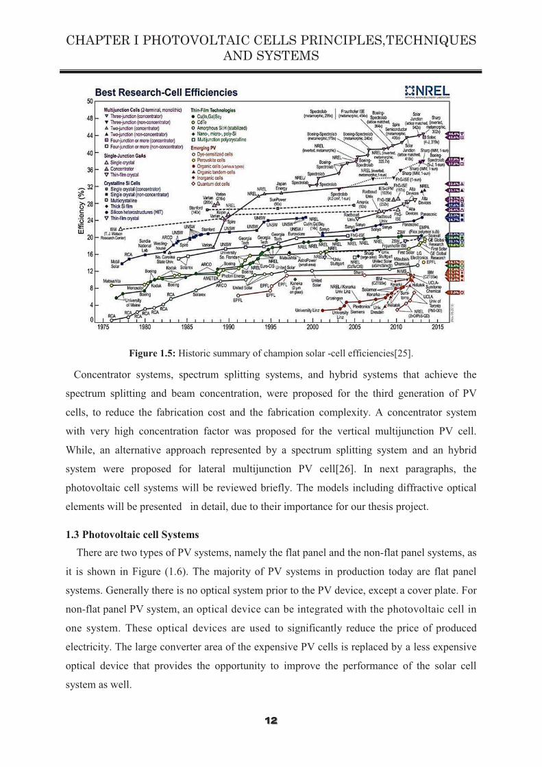
CHAPTER I PHOTOVOLTAIC CELLS PRINCIPLES,TECHNIQUES
AND SYSTEMS
'�
Figure 1.5: Historic summary of champion solar -cell efficiencies[25].
Concentrator systems, spectrum splitting systems, and hybrid systems that achieve the
spectrum splitting and beam concentration, were proposed for the third generation of PV
cells, to reduce the fabrication cost and the fabrication complexity. A concentrator system
with very high concentration factor was proposed for the vertical multijunction PV cell.
While, an alternative approach represented by a spectrum splitting system and an hybrid
system were proposed for lateral multijunction PV cell[26]. In next paragraphs, the
photovoltaic cell systems will be reviewed briefly. The models including diffractive optical
elements will be presented in detail, due to their importance for our thesis project.
1.3 Photovoltaic cell Systems
There are two types of PV systems, namely the flat panel and the non-flat panel systems, as
it is shown in Figure (1.6). The majority of PV systems in production today are flat panel
systems. Generally there is no optical system prior to the PV device, except a cover plate. For
non-flat panel PV system, an optical device can be integrated with the photovoltaic cell in
one system. These optical devices are used to significantly reduce the price of produced
electricity. The large converter area of the expensive PV cells is replaced by a less expensive
optical device that provides the opportunity to improve the performance of the solar cell
system as well.

CHAPTER I PHOTOVOLTAIC CELLS PRINCIPLES,TECHNIQUES
AND SYSTEMS
'
-a-
-b- Figure 1.6: Photovoltaic cell systems:
a- Flat panel PV cell system b- Non-Flat PV cell system.
1.3.1 Flat Panel Photovoltaic cell Systems
In these systems, the sunlight goes directly to the PV device without any focusing. The
light without concentration can be collected from any angle by a flat panel system, as shown
in Figure (1.7). Therefore, the flat panel system can collect and convert diffuse light from the
sky (or light reflected from the ground snow, etc.) as well as direct sunlight.
Figure 1.7: Flat panel PV cell system.
The flat panel PV systems can collect light over an entire hemisphere without the need to
use a tracking system to retain the PV cell surface perpendicular to the sun rays. In this case,
there is no major change in the weather conditions, such as the cloud cover which is expected
to prevent the absorption of light. Therefore, the contribution from the diffuse light stays
approximately the same throughout the day. However, as the sun moves across the sky, the
projected area of the flat panel depends on the relative position of the sun to the panel. The
projected area, Aproj, is defined as:

CHAPTER I PHOTOVOLTAIC CELLS PRINCIPLES,TECHNIQUES
AND SYSTEMS
'!
(1.3)
Where (A) is the area of the panel and (θ) is the incidence angle of the sunlight on the panel
about the vertical axis. When the sunlight is not perpendicular to the PV cell panel, there is a
significant reduction in the amount of sunlight that the PV cell can collect and convert into
electrical energy. The dual-axis tracking system is used to position the PV cell panel
normally to the sunlight incidence, to avoid the decrease of power output owing to the change
of the exposure area.
1.3.2 Non-Flat Panel Photovoltaic cell System
In general, non-flat PV systems can be classified into three types by depending on the
optical device which is added to the photovoltaic cells; the concentrators PV cell system,
the spectrum splitting PV cell system, and the hybrid system that can achieve both
functions of beam concentration and spectrum splitting simultaneously. Multi-tandem
solar cell fabrication is expensive and the manufacturing process can cause significant
environmental pollution. Non-flat Photovoltaic cells systems offer several benefits compared with
conventional flat PV mono-junction cells devices. Firstly, the production efficiency is higher.
Secondly, it makes use of less semiconductor material what contributes not only to reduce the
cost, but also helps to reduce the pollution associated to the manufacturing process. Thirdly, the
systems have a higher efficiency especially for hot and sunny locations.
I. Concentrator Photovoltaic cells systems
Concentrated photovoltaic cells (CPV) systems use optical devices such as lenses or
mirrors to concentrate the incident sunlight onto a small photovoltaic solar cell area. The
concentrators system are classified into different classes depending on the optical means
used to concentrate the light, and the number of axes about which they move to track the
sun[17]. Most concentrator systems operate according to the principles of reflection or
refraction, furthermore some concentrator systems operate by a diffraction effect such as non-
imaging Fresnel lens. Concentrator PV cells systems become attractive, due to the significant
growth in the commercial usage of the high-efficiency–multi-cascade solar cells.
Multijunction PV cells techniques demonstrated the ability to achieve photovoltaic
conversion efficiencies around 40-50 %. The purpose behind the utilization of the
concentrator system is to reduce the very expensive cost per square centimeter of the high
efficiency photovoltaic cell. The majority of the PV cell area is replaced by the concentrator

CHAPTER I PHOTOVOLTAIC CELLS PRINCIPLES,TECHNIQUES
AND SYSTEMS
��
system, which is usually cheaper than PV cells. Generally, the global manufacturing of a high
efficient PV cell is much more expensive than it is for the traditional silicon PV cells[27].
The advantage of the concentrator system is to provide the ability to increase the efficiency of
photovoltaic cell. However, other limitations appear due to the heat problem which leads to
increases in the cell resistance losses. The selection of an optimal concentrator system for
any solar cell system is based on the properties of photovoltaic cell[28].
The concentrator helps in reducing the cost of solar cell system, but it also adds complexity
and costs in other ways. Furthermore, it also decreases the acceptance angle or the largest
incidence angle at the front of the concentrator aperture in the input of the PV cell system.
The amount of sunlight that can be collected by the solar cell system depends on the étendue
of the concentrator. When, the purpose is to collect sunlight throughout the whole day at the
highest concentration, it is necessary to use a tracking system, to ensure that sunlight will be
focused by the concentrator, at vertical incidence on the PV cell surface. The tracking system
significantly adds complexity to the process of combining the optical device with the PV cell
in a solar cell system.
The concentrator photovoltaic cells systems require to choose the optimum between several
parameters to obtain the highest possible efficiency at the lowest price. We will review the
most important parameters to be considered for a concentrator design that will have
remarkable effects on the PV cell operations.
i. Concentration Ratio
The concentration ratio is defined as the ratio between the width, or the area, of the
concentrator (AC) and the PV cell (APV).
(1.4)
The geometric concentration factor is defined by the intensity concentration unit (X) or "sun
unit" that is equal to (1000 w/m2). Therefore, the CPV cells systems can be classified into
three types depending on the concentration ratio:
1. Low concentrator
2. Medium concentrator
3. High concentrator

CHAPTER I PHOTOVOLTAIC CELLS PRINCIPLES,TECHNIQUES
AND SYSTEMS
�
Where, Cmax is the maximum concentration factor which takes the value 208 for a line
focusing concentrator (2D) and (43400) for a point focusing concentrator (3D). The factor of
geometrical concentration for the actual devices varies from the ideal by factor 2-10 for linear
design and by about 5-30 for 3D concentrators (>100). Usually, the concentrator that performs
a high concentration ratio is preferred for use in a solar cell system; because it gives the greatest
reduction in cell area used which leads to reduction in the fabrication costs as well. However,
sometimes the high concentrator PV cells systems need to use additional parts such as a heat sink
and tracking systems.
ii. Optical Efficiency and Effective Concentration
The second important parameter to assess the efficiency of a sunlight concentrator system is
its optical efficiency. It is the percentage of light entering the concentrator that reaches the
PV cell. It can be defined as the ratio between the flux absorbed (ФPV) by the photovoltaic
cell to the flux of incident sunlight (ФC) on the concentrator system:
(1.5)
The design principle is to make the optical efficiency as high as possible. However, due to
different types of losses, such as, Fresnel losses or material absorption losses or light entering the
system but that is not collected by the solar cell etc., the optical efficiency cannot be
100%. Another factor called the optical concentration is used also to assess the concentrator
performance. This factor is defined as the multiplication of the geometric concentration ratio
with the optical efficiency:
(1.6)
There are also several parameters that have significant effects on the performance of a
concentrator in a photovoltaic cell system, such as the acceptance angle, the irradiation
uniformity and the etendue. They are not under study in this thesis.
For a clear understanding of the concentration effect on the PV cell system operation, the
influence of the concentration factors on the PV cell efficiency will be explained in the next
paragraph.

CHAPTER I PHOTOVOLTAIC CELLS PRINCIPLES,TECHNIQUES
AND SYSTEMS
�!
a. Physical effect of the concentrator factors on the PV cell efficiency
The concentrator photovoltaic cell system has a better performance than a non-
concentrated PV cell system, both in manufacturing and in the ability to convert sunlight to
electricity at a higher efficiency. The conversion efficiency (η) of photovoltaic cell under
non-concentrated radiation is defined[29]:
(1.7)
Where Pin is the optical input power (irradiance) and (APV) is the area of the photovoltaic cell.
The short-current circuit density increases linearly with an increasing in the optical
concentration factor, as follows:
(1.8)
Where is the short-circuit current generated by the photovoltaic cell with the irradiance E,
which is equal to one sun (1000 W/m2, and standard spectrum). While, the open-circuit
voltage Voc increases logarithmically as:
(1.9)
The zero in the subscript denotes the case of one-sun irradiation. The nVth represents the
temperature dependency of the efficiency of the cell (n is a diode quality factor of the cell and
Vth is the thermal voltage).
Now, the conversion efficiency η of a photovoltaic cell under concentrated light, kept at
constant temperature, can be defined as a function of optical concentration factor:
(1.10)
The physical conversion efficiency of photovoltaic cells increases for high quality
concentrator cells, until even their low series resistances create losses, what cause the total
efficiency to drop sharply.
b. Nonimaging Fresnel lenses (Fresnel lens concentrator system)
Non-imaging system using convenient Fresnel lenses provides the possibilities necessary for
the commercial fabrication of the solar energy concentrator, for the photovoltaic and the

CHAPTER I PHOTOVOLTAIC CELLS PRINCIPLES,TECHNIQUES
AND SYSTEMS
�"
thermal conversion. Compared with imaging systems, nonimaging systems have the
advantages; of larger acceptable angles, higher concentration ratios with less volume, and
shorter focal length, higher optical efficiency along with minimal weight and low cost , etc.
The most widely used high concentrator PV cell systems consist of refractive Fresnel lenses
which produce a point-focus.Compared to a conventional lens, a Fresnel lens reduces the use
of the constituting material and make the whole system thinner and lighter. Light absorption
is lowered because of shorter optical path length in a thinner lens. A Nonimaging Fresnel lens
offers the possibility to design a stationary concentrator with a low concentration ratio, a low
precision tracking and it allows a more uniform flux density. A Fresnel lens can provide
either point-focus, when it has a circular symmetry about the optical axis, or linear focus,
when the lens has a constant cross section along a transverse axis [17], as its shown in Figure
(1.8). Such lenses focus the light into a line in one dimension, or into a strip (line-focus lenses
have a linear array of cells). This type is used in thermal concentrator solar system, which is
also called concentrator solar power (CSP) and in low concentrator PV cells systems.
Whereas, point-focus lenses usually use one cell behind each lens. They are an attractive
alternative to hot embossed or injection molded lenses in High Concentration Photovoltaic
(HCPV) application. The first attempts to use Fresnel lenses for the collection of solar energy
occurred at the time when suitable plastics such as polymethylmethacrylate (PMMA) became
available in the 1950s. PMMA is resistant to sunlight, and remains thermally stable up to at
least 80◦C. It has a transmissivity that matches the solar spectrum, and its refractive index is
1.49, which is very close to that of glass [30]. Consequently, most Fresnel lens designers for
concentrator solar energy systems, selected PMMA as a material for the lenses, because of its
high optical quality combined with less expensive manufacturing technologies. The work of
W.T. Xie that is mentioned in ref. [31] represents a good reference for the Fresnel lens
concentrator techniques.

CHAPTER I PHOTOVOLTAIC CELLS PRINCIPLES,TECHNIQUES
AND SYSTEMS
�#
Figure 1.8: Fresnel lens concentrator configuration [17]. a- Point focus concentrator. b- Linear focus concentrator.
c. Review of the distinctive concentrator system researches
Recently, several distinctive prototypes were proposed as solar concentrators systems. Much
research adopts the idea of combining the non-imaging flat Fresnel lens, as the primary
optical elements (POE), with secondary optical elements (SOE), to produce a light
homogenization (to homogenize the flux distribution) on the PV cell surface [30-32]. Jason
H. Karp[33] presented different approaches for a planar micro-optic solar concentrator, by
coupling the two -dimensions lens array with planar waveguides. Several models of the solar
concentrators system were designed depending on the diffractive optical elements
characteristics, such as combining a wedge prism and a diffraction grating [34], holographic
optical elements [35, 36] and subwavelength gratings [37].
II. Spectrum splitting PV cells systems
An alternative strategy was used to reduce the cost of solar electricity production, and to
increase system efficiency of the modules, through the use of spectrum splitting techniques.
The theoretical maximum efficiency for a single junction photovoltaic cell under
unconcentrated sunlight is 33.5%[38]. The restriction on the efficiency of photovoltaic cell
is defined by the Shockley-Read-Hall equation. Therefore, this constraint limits the sun
spectrum range that can be converted into electric energy by a solar cell. Increasing the
system efficiency can be achieved by increasing the number of the solar cells with different

CHAPTER I PHOTOVOLTAIC CELLS PRINCIPLES,TECHNIQUES
AND SYSTEMS
$%
characteristics used in the system, to ensure more efficiently sunlight conversion into
electricity.
In theory, dividing the spectrum into several bands and directing each band to a matched
PV cell, can provide very high conversion efficiency. The concept of harvesting solar energy
by splitting the solar spectrum and directing each band to the most efficient converter, was
proposed for the first time by Jackson[39] in 1950. The first experimental work was
demonstrated by Moon et al.[40], in 1978. A “perfect” solar cell energy conversion system
will be capable of exploiting the entire incident broadband solar spectrum, through thermal
and electrical conversion processes. Increases of the conversion efficiency in the solar cell
system can be obtained in three ways:
1. Shifting the solar spectrum towards wavelengths that are more efficiently
converted by the PV cell, as seen in thermo-photovoltaic (TPV) and
luminescent concentrators.
2. Stacking PV cells of different materials and different band-gaps in series or
parallel to absorb a larger part of the solar spectrum.
3. Splitting the solar spectrum to run several photovoltaic and thermal process in
parallel, combining moderate to high-temperature thermal conversion with
efficient PV conversion.
Photothermal processes convert solar energy into heat with a relatively constant efficiency,
over the solar spectrum. A photovoltaic conversion process is highly wavelength-dependent
and is most efficient when converting photons having energy close to the PV cell band-gap.
This is because, photons with energy less than the band-gap energy pass through the active
area of the cell without being absorbed, and are ultimately dissipated, as heat in other parts of
cell. Photons of energy higher than the band-gap energy can only be partly used and the
remaining sunlight energy is also dissipated as heat. For this reason, the concept of an hybrid
PV/thermal solar concentrator system has been adopted to achieve high conversion efficiency
in a solar system, the incident beam is split in this case into PV and thermal spectral
components, as illustrated in Figure (1.9-a). The PV/thermal solar cell system produces
electricity by combining the operations of the photovoltaic conversion and the thermal
conversion. In addition, the high conversion efficiency for the entire sunlight spectrum, could

CHAPTER I PHOTOVOLTAIC CELLS PRINCIPLES,TECHNIQUES
AND SYSTEMS
$�
be achieved by using the photovoltaic effect only, by adopting the working principle of the
third generation cell (tandem solar cell) as illustrated in Figure (1.9-b).
-a-
-b-
Figure 1.9: Splitting the solar spectrum into components[26]: a- PV and thermal energy conversion. b- Triple-junction tandem solar cell conversion.
The working principle for the third generation cells, depend on the use of many PV cells
that have different band gaps. Therefore, the conversion of the entire sunlight spectrum that
can be achieved leads to increase the efficiency of solar cells systems. The third generation
solar cells can be classified into two kinds, based on the methodology used to arrange the
multiple junctions of the PV cells:
i. Vertical multijunction PV cells system
In this kind of cell, the multiple junctions of the different PV cells are stacked vertically in
a single PV system. Each junction can convert the portion of the solar spectrum having
energy greater than its energy gap. The band gap of each junction decreases from top to
bottom.
Thus, the photons that have a high energy are absorbed at the top junction, while
subsequent junction absorbs the photons of lower energy. A multijunction PV cell has the
potential to convert a large portion of the solar spectrum into electricity by converting the
sunlight more efficiently compared to a single junction. Figure (1.10) shows the amount of
the solar spectrum that can be converted by a single junction PV cell compared to an example
of triple junction’s solar cell. In 2015, the world efficiency record for a PV cell is held by a
triple junction device under concentration, with efficiency equal to 44.7%.

CHAPTER I PHOTOVOLTAIC CELLS PRINCIPLES,TECHNIQUES
AND SYSTEMS
$$
Figure 1.10: The AM1.5 solar spectrum and the parts of the spectrum that can be used in theory by[41]:
a- Si PV cell. b- Ga0.35In0.65As/Ge PV cells.
This type of third generation cell has some disadvantages owing to the complexity of the
fabrication processes, and they are also expensive. The PV cells are fabricated by using the
epitaxially grown technique [42] or the mechanically stacked technique[43]. Mechanically
stacked PV cells can suffer from significant optical losses due to the reflections at the
interface. Epitaxially grown cells suffer from the challenge of fabricating junctions with
combinations of band gaps that are optimal for solar spectrum. The epitaxially grown
technique requires lattice matching, and a tunnel junction at the interfaces between each p-n
junction, this limits the possibility of material combining. In addition, the current produced
by each junction must stay the same, because the junctions are typically serially connected.
All these restrictions increase the complexity of the fabrication process. Concentrator systems
are preferably used for this type of third generation cells, in order to reduce the fabrication
cost. While, the separation of the spectrum is achieved via the tandem multijunction PV cell,
as explained above, without need to use the spectrum splitting systems.

CHAPTER I PHOTOVOLTAIC CELLS PRINCIPLES,TECHNIQUES
AND SYSTEMS
$&
ii. Lateral multjunction PV cells systems
An alternate model of third generation cells is proposed to overcome the restrictions
imposed by the fabrication processes on the previous type. In this kind, the multiple junctions
of the different PV cells are placed in parallel in a single PV cell system. The sunlight
spectrum is separated by the spectrum splitting system, and then redirected into each PV cell.
This model offers the best flexibility for the fabrication processes of the third generation
cells. Each PV cell can be fabricated independently and can be rearranged later on one plate,
which also allows increase in the number of PV junctions in a solar cell system. Figure
(1.11) illustrates the method of collecting the sunlight spectrum by the both types of the third
generation cells. The lateral multijunction PV cell system can achieve a high electricity
production performance, when choosing an appropriate spectrum splitting system.
-a-
-b-
Figure 1.11: Methods of collecting the sunlight spectrum by the third generation cells. a- Vertical multijunction PV cell systems[44]. b- Lateral multjunction PV cells systems[45].
a. Spectrum splitting techniques
The design of a spectrum splitting system depends on several optical phenomena, such as:
interference, refraction, and diffraction. Therefore, several models of splitting operating by
filtering techniques have been proposed that are based on these phenomena, such as thin film
filters, luminescent concentrators, prismatic elements, and diffractive/holographic elements.
Firstly, the filtering technique was achieved through interference. Primarily via the use of
dichroic (thin film filter) and multilayer mirrors, to validate the spectral splitting for

CHAPTER I PHOTOVOLTAIC CELLS PRINCIPLES,TECHNIQUES
AND SYSTEMS
$'
photovoltaic cells systems [46, 47]. However, the geometry of such devices precludes a
specific scaling for large areas which limits the number of bands that can be effectively
separated. Secondly, the filtering technique was achieved through refraction. The prisms
allow a spectrum separation via the dispersive refraction. Unfortunately, they are impractical
for scaling to large areas due to the volume and weight requirements. Furthermore, they
provide very little control over the spatial position of bands as well as the selection of the
band edges. Thirdly, the filtering technique was achieved through diffraction. Conventional
gratings enable a spectral separation via diffraction. Unfortunately, they typically suffer from
low diffraction efficiency, as well as a poor control of the spatial position of the spectrum
bands. The work of Ahmad Mojiri et al [48] and Imenes [26] represent two relevant reviews
of the spectrum splitting systems that have been designed and tested.
Nowadays, the diffractive optical elements represent the most effective technology
compared with the other filtering techniques, owing to several reasons: First, from the
performance viewpoint, the diffractive optical elements can achieve a good control of the
spatial positions of the spectrum bands with a high efficiency. Second, from a fabrication
viewpoint, the remarkable progress in the technology of photolithography makes it possible
to fabricate of these elements by using light and cheap materials, and for building an optical
system that can be integrated into a photovoltaic cell. Therefore, a compact solar cell system
can be realized practically by using DOE’s.
b. Review for the distinctive spectrum splitting system proposed
Recently, several distinctive prototypes were proposed for spectrum splitting systems. The
main research relies on the filtering of the sunlight spectrum through the effect of the
absorbance/transmittance or the effect of reflectance/transmittance. The proposed technology
consists of one plate (with one layer, or several layers), or several plates which include: all-
dielectric and metal -dielectric multilayer filters[49, 50], heat reflectors[51, 52], refraction
and prism for spectrum splitting[53, 54], holographic filters[55, 56], fluorescent device and
method[57, 58] liquid absorption filters[59].
III. Hybrid PV cells systems
The cost of solar cell systems that use spectrum splitting systems is usually higher than the
cost of standard solar cells systems. Spectrum splitting systems also cause a higher
complexity for assembling the final solar cell system. Several types of optical losses are

CHAPTER I PHOTOVOLTAIC CELLS PRINCIPLES,TECHNIQUES
AND SYSTEMS
��
produced by this system, owing to: sloped transition from reflection to transmission, non-
ideal cutoff wavelengths and reflection losses of the mirrors. Therefore, for a commercially
viable fabrication of these solar systems, it is necessary to minimize the optical losses. The
hybrid PV systems that achieve spectrum splitting and beam concentration have been
proposed for providing solutions for this problem.
In the literature, the hybrid PV systems are classified into two categories:
i. Non-compact hybrid system
In this system, the functions of beam concentration and spectrum splitting are obtained
through the use of two independent optical devices. These devices include a concentrator
composed of lenses or dishes, combined with a spectrum splitting device, which is placed
close to the focus position of the light by the previous device. Several designs of non-
compact hybrid solar systems have been proposed, they are reviewed below:
Zhao and Sheng[60] proposed a hybrid solar cell system, that is composed by an
assembly of lenses and consecutive selective mirrors, as shown in Figure (1.12). In
this solar system, five single junction photovoltaic cells were used, with four optical
filters. This model succeeded to realize efficiency about 35.6 % under a
concentration ratio of 2.8 SUN (AM1.5G) radiation. It is expected to achieve a
value of 52.9% of the conversion efficiency for the PV cells that have a “perfect
diode structure”.
Figure 1.12: Schematic diagram of the optical path with five photocells and four filters in the spectrum splitting solar photovoltaic conversion system [60].
D. Lin et al [61] presented a hybrid solar cell system consisting of an holographic
element operating as lossless spectrum splitting, combined with a concentration lens

CHAPTER I PHOTOVOLTAIC CELLS PRINCIPLES,TECHNIQUES
AND SYSTEMS
�
that is arranged, as shown in Figure (1.13). In this system, the solar spectrum is
separated into two bands, which can be absorbed by two laterally arranged PV cells.
P. Bentiez et al [18] proposed a new model of a concentrator spectrum splitting PV
cell system. It is composed of two optical elements, which achieve a high
concentration ratio, as shown in Figure (1.14). The first element of this system is a
flat Fresnel-Kohler lens, and the second optical element is a free-form Kohler
RXI-RR concentrator with an embedded flat band-pass filter. This device performs
a conversion efficiency of about 43%, when the incident sunlight is separated into
two bands with a concentration ratio of 300X. The first band is absorbed by a
silicon cell while the second band is absorbed by three PV junctions (3J) tandem
cells (GaInP/GaInAs/Ge).
Figure 1.13: Schematic for a non-compact hybrid system for two lateral PV cells [61].
Figure 1.14: Kohler RXI-RR SOE concentrator, with the flat band-pass filter and the 3J and BPC silicon cells [18].
Goetzberger [62] et al., suggested different design depending on the advantage of
using a trapping effect, to achieve sunlight concentration, as shown in Figure (1.15).
This system consists of lenses which concentrate the light and pass through a small
hole to the trap cavity. The radiation inside the trap cavity is transformed to a

CHAPTER I PHOTOVOLTAIC CELLS PRINCIPLES,TECHNIQUES
AND SYSTEMS
�!
diffuse light, by using randomized lambertian (diffuse) reflectors. Each PV cell,
inside the trap cavity is covered by a bandpass mirror, which transmits the optimal
wavelength and reflects the rest of the sunlight spectrum.
Figure 1.15: Schematic diagram of the concentrator spectrum splitting PV cell system, light is concentrated by lenses and trapped inside cavity that contains the PV cells, which are covered by a
bandpass mirror [62].
ii. Alternative compact hybrid solar cell system (CHSCS)
An alternative compact hybrid solar cell system was proposed. It is used to implement both
functions of the beam concentration and the spectrum splitting for sunlight simultaneously.
This system has several important advantages, which are represented by improving the
performance and reducing the complexity and the cost of the fabrication process. The optical
losses produced by this system are less important due to the limited number of the
interference surfaces, which lead to reductions in reflection, and absorption losses. The
integration of the concentrator and the spectral splitting devices in a single optical component
allows fabrication of a compact solar cell system that is characterized by a high efficiency.
Furthermore, these compact hybrid systems have low fabrication costs through the use of
well-established industrial technologies. Several designs of compact hybrid solar systems
have been proposed, they will be reviewed below:
Marco Stefancich [63] et al presented a compact solar system, consisting of a
single low-cost plastic prismatic structure, as shown in Figure (1.16-a). This system
simultaneously achieves both beam concentration and spectrum splitting of
sunlight. This device exploits the prism material performance to achieve a high
accuracy spectral separation.

CHAPTER I PHOTOVOLTAIC CELLS PRINCIPLES,TECHNIQUES
AND SYSTEMS
�"
Vencenzi [64] Donato et al suggested a different approach for compact solar
systems based on dichroic concentration mirrors, as shown in Figure (1.16-b). The
spectral separation was obtained by means of a short-pass dichroic filter that
covered the inner mirror. The spectrum band containing the long wavelengths is
reflected towards the high band gap PV cell by a dichroic concentration mirror.
While, the spectrum band containing the short wavelengths, is transmitted through
the filter and then reflected back towards the low band gap PV cell by a wideband
mirror.
-a-
-b- Figure 1.16: Compact PV cell systems.
a- Schematic diagram of a concentrator/ spectral splitting system that is consisting in a set of prisms[63]
b- Concentrator and spectrum splitting system that consists of the dichroic mirrors [64].
a. Diffractive optical elements in CHSCS design
Diffractive optical elements (DOE) have been proposed since the 1970’s[65] for the
optimization of the incident light radiation power management in solar energy systems. DOE
were not only used for fine-tuning of the optical properties of input surfaces with respect to a
wavelength selective absorbance, but also for the smart steering of the light radiation. Several
designs of compact hybrid PV cell systems were proposed. They consisted of a diffractive
optical element. In some cases, the diffractive optical element represents all the optical
system or it is part of a large optical system. The diffractive optical elements are preferably
used to improve solar systems instead of other optical elements, owing to several positive
aspects;
1. The Performance factor: DOE’s offer a very high control for the spatial separation of
the spectral bands. In addition, they have the possibility to achieve high diffraction
efficiency for a large spectrum band of sunlight.

CHAPTER I PHOTOVOLTAIC CELLS PRINCIPLES,TECHNIQUES
AND SYSTEMS
�#
2. The Fabrication factor: DOE’s can be realized from light, cheap materials with a
planar form, and can be replicated even for large area devices. Moreover, DOE can be
integrated in a compact photoconversion solar cell system.
b. Review of the distinctive research on CHSCS including diffractive optical elements
Over the last years, several researchers provided the idea of using diffractive optical
elements, in the design of a compact hybrid solar cell system. We now review the most
important researches proposed on CHSCS using the diffractive optical elements, as follows:
Jose M. Castro [66] presented a model of CHSCS consisting of two planar
holographic optical elements (HOE), stacked in cascade to implement spectrum
splitting and beam concentration (SSBC) simultaneously, as shown in Figure (1.17-
a). This design was used to maximize the light energy collection efficiency during
the course of a year without the need for a tracking.
Michael Gordon [20] presented an alternative design of a CHSCS, consisting also
from aggregation of two planar holographic optical elements (HOE), but this time
they are placed side by side to achieve SSBC both in transmission and in reflection,
as shown in Figure (1.17-b).
-a-
-b- Figure 1.17: Schematic diagrams of CHSCS that is consisting of two holographic optical elements
and two PV cells. a- Holographic optical element arranged vertically [66].
b- Holographic optical element arranged laterally [20].
Céline Michel [67] proposed a new design of a planar solar concentrator for space
applications. In this model, a blazed diffraction grating is superimposed to a
refractive Fresnel lens, on the opposite sides (double sided) of the optical system, as
shown in Figure (1.18-a). This model focuses sunlight onto two PV cells spatially
separated, with a high concentration ratio.

CHAPTER I PHOTOVOLTAIC CELLS PRINCIPLES,TECHNIQUES
AND SYSTEMS
$%
Ye Jia-sheng [68] proposed a single diffractive optical element (DOE) for
implementing spectrum splitting and beam concentration functions simultaneously,
as shown in Figure (1.18-b). In this design, a blazed diffraction grating is
superimposed to a diffractive Fresnel lens, in one side (single sided) of the optical
system. This design allows the focusing of sunlight onto several PV cells, spatially
separated, with a high concentration ratio.
-a-
-b- Figure 1.18: Schematic diagrams of a CHSCS that is consisting in merging a grating to a lens.
a- Grating profile and lens profile arranged in a double sided way [67]. b- Grating profile and lens profile arranged in a single sided way [68].
Ganghun Kim [19] presented a new paradigm of the diffractive optical element for
a photovoltaic application, as shown in Figure (1.19). This unconventional approach
is used to design multilevel broadband diffractive optical elements, it depends on a
conventional binary-search algorithm. This design allows focusing of sunlight onto
two PV cells that are spatially separated, with a low concentration ratio.
Figure 1.19: Schematic diagram of a single DOE that implements SSBC functions simultaneously [19].

CHAPTER I PHOTOVOLTAIC CELLS PRINCIPLES,TECHNIQUES
AND SYSTEMS
$&
Yuhan Yao [21] presents a design of a high-efficiency dispersive mirror based on a
multi-layer dielectric meta-surface. These dielectric meta-surfaces have been designed
from a high-index-contrast sub-wavelength gratings. The spectrum splitting was
achieved through an optimization process of the sub-wavelength structure for each
layer. Each layer reflects a certain spectrum band from sunlight into a particular
direction.
Figure 1.20: Schematic of a reflective setup integrated with a solar cell that is consisting of a multi-layer of dielectric meta-surface (subwavelength structure) [21].
1.4 Conclusion
In conclusion, this chapter presented a brief review of the different types of photovoltaic
cells and of solar cells systems. We can conclude that the third generation PV cells represent
a promising candidate for solar energy production, because of their high conversion
efficiency compared to the other types of PV cells. The third generation cell requires a
complex fabrication process and a quite high manufacturing cost. Therefore, several types of
photovoltaic cells systems have been proposed to reduce these restrictions. The concentrator
system that is preferred for the third generation cells is of the vertical type. While, the
spectrum splitting system and the hybrid concentrator spectrum splitting system are preferred
with the third generation cell of the lateral type. The technique of lateral type of the third
generation cells have many advantages compared to the vertical type of the third generation
cell; easy to fabricate, no limitation on the numbers of p-n junctions, and the possibility to
exploit the whole sunlight spectrum. The lateral type third generation can achieve a higher
electricity production efficiency, and can constitute an attractive photovoltaic cell system.
The hybrid concentrator spectrum splitting system that includes the diffractive optical
elements, represents the ideal device for a high photoconversion efficiency at reasonable cost.

CHAPTER I PHOTOVOLTAIC CELLS PRINCIPLES,TECHNIQUES
AND SYSTEMS
$�
Diffractive optical elements can achieve a good control and a good management of the
incident sunlight for large spectrum bands. Furthermore, diffractive optical elements can be
manufactured from cheap and light materials; they can be used for large surface with a thin
thickness, what allows building compact photovoltaic cells systems. In the next chapter, the
diffractive optical element will be presented with clarification for its modelling and designing
methods.

CHAPTER II DIFFRACTIVE OPTICAL ELEMENTS MODELLING AND DESIGN METHODS
$$
2.1 Introduction
This chapter introduces a general review oriented towards the diffractive optical elements
(DOE’s) physics and technologies. A general classification for the DOE’s will be presented,
it will be based on three important factors; the DOE structure profiles, the functions required
from the DOE, and the methods used for the modelling and design of the DOE. The
diffraction theories that are used for modelling and designing different types of DOE’s will
be presented. The characteristic of theories will be explained in detail. This will help to fix
our choice for the calculation tools that will be used for the design of our DOE. Thus, we will
conclude the optimized diffraction theory that can be used in the design and the modelling the
targeted DOE.
2.2 Diffractive Optical Elements (DOE) presentation
The diffractive optical elements (DOE’s) are optical devices presenting a microscopic
depth profile, which are composed of micro, or nano patterns and that control light
propagation through diffraction phenomenona. DOE’s are designed to deal with light
wavefronts by segmenting and redirecting the incident light through the use of interference
and phase control [1]. As such, diffractive optics is a subfield of physical optics, which deals
with all forms of propagation of electromagnetic waves. There is an increasing interest from
the optics community in DOE's, owing to three main reasons. Firstly, DOE’s play an
important role in increased range of applications in modern optics. Such as; micro-optics,
nano-optics, integrated optics, and micro-opto-electromechanical systems (MOEMS).
Secondly, the progress in computer science and technology allows, to design and to simulate
the performance of complex DOE's with a high accuracy. Thirdly, the progress in the micro
and nano fabrication technology offers the possibility to fabricate DOE's from light and
inexpensive materials even if they have a very small feature size. Therefore, compact optical
systems can be fabricated from DOE's, with superior miniaturization features.
2.3 Classification of Diffractive optical elements
Generally a diffractive optical element is designed for a particular application by
implementing a specific function that depends on its characteristics. Therefore, a selection of
the methods for the modelling and the designing, as well the fabrication technique can be
used for manufacturing of such DOE’s. This would depend on the functionalities
implemented and the characteristics of the considered DOE's. There are several kinds of DOE
CHAPTER II DIFFRACTIVE OPTICAL ELEMENTS MODELLING AND DESIGN METHODS
$'
classifications that are used in the literature for organizing the categories of DOE's. These
classifications are based on three main criteria’s which include subclass criteria’s;
i. Classification of DOE's by their depth profiles.
· Super-wavelength DOE's[69]: their feature size is bigger than the wavelength.
· Sub-wavelength DOE's[69]: their feature size is smaller than the wavelength.
· Binary DOE's[1]: they have discrete numbers of the phase-controlling surfaces.
The simplest form has two depth profiles only, which produce both a 0 and π-
phase or 0 and 2π-phase difference on the incident light wavefront. They can be
produced by using one lithographic mask only. The second form is relative to
multilevel binary DOE’s, which have 2N depth profiles and usually produce 2N
phase shift levels. They can be produced by using N lithographic masks.
· Kinoform DOE's[1]: they present a smooth variation of the phase-controlling
surfaces.
· Computer-Generated Hologram[1]: A DOE that is generated by reducing a
calculated interference pattern to a series of phase or amplitude masks. It is
similar to other diffractive optics elements, except that the targeted wavefront
form will be used to generate the final DOE pattern.
· Holographic Optical Element[1]: A DOE generated by the interference of two
wavefronts to produce a component that can be used to act as an optical
component. (The distinction between this element and a hologram is that a
hologram is usually intended to record some elaborate scene.)
· Thin DOE's (nonharmonic)[71]: they have a thickness (depth profile), which
produces a phase shift equal or smaller than 2π.
· Thick DOE's (harmonic)[71]: they have a thickness (depth profile), which
produces multi-harmonic degrees of phase shift 2p (p=2, 3, …).
· Periodic DOE's' structure[71]: they present profile structure that consists in a
periodic pattern.
· Non-periodic DOE's structure[71]: they present profile structure that consists in
non-periodic patterns.
ii. Classification of DOE’s by the function implemented [69].

CHAPTER II DIFFRACTIVE OPTICAL ELEMENTS MODELLING AND DESIGN METHODS
��
· Transmission DOE's: the diffraction patterns are produced on the opposite side of
the light source used.
· Reflection DOE's: the diffraction patterns are produced on the same side as the
light source.
· Amplitude DOE's: they modulate the amplitude of the propagated light by
absorption inside the profile structure.
· Phase DOE's: they modulate the propagation of light without absorption, only with
a modulated phase, according to the phase shift produced by the profile structure.
· Fourier DOE's: they produce the diffraction patterns in the far-field (in the order of
decimeters). This type of DOE usually acts as a diverging element, e.g. as a beam
splitter, and as a beam shaper, where the diffraction pattern is larger than the DOE
size.
· Fresnel DOE's: they produce the diffraction patterns in the near-field (in the order
of millimeters). This type of DOE usually acts as a converging element, e.g.
microlens, where the diffraction pattern is smaller than the DOE size.
iii. Classification of the calculation methods used in the design and modelling of the
DOE's performances[69].
· Analytical method: A DOE is designed and its performance modelled, by using
analytical equations. This method is used in some rare cases, and for some specific
types of DOE’s.
· Numerical method: A DOE can be designed and the modelling of its performance
achieved by using numerical algorithms. This method is usually used for the
majority of DOE’s types.
2.4 Diffraction theories generally used for diffractive optical elements
Several phenomena occur when light propagates through a diffractive optical element, such
as, refraction, reflection, diffraction and diffusion. Therefore, the electromagnetic wave
nature of light will be used to explain those phenomena. The electromagnetic wave behavior
of light can be described by the Maxwell's equations. Generally in the literature, two models
of diffraction theories have been used, to describe all phenomena related to the light
propagation through the DOE's: Scalar Diffraction Theory (SDT), and Rigorous Diffraction
Theory (RDT). The main difference between these two theories is the way that solves the
Maxwell's equations. In SDT the Maxwell equations are solved with an approximation that

CHAPTER II DIFFRACTIVE OPTICAL ELEMENTS MODELLING AND DESIGN METHODS
�
consists to deal with only one field component associated either to the E or the M field. On
the contrary with the RDT, Maxwell's equations are solved rigorously, without any
approximations, and they deal with the interaction between all electromagnetic components
(E and M). The selection of the appropriate diffraction theory, which can be used for
modelling and designing any DOE's depends on two factors: the DOE structure
characteristics that are desired and the intended function to be implemented by a DOE.
I. Depending on the structure characteristic of DOE's
There are basically two main parameters that determine which diffraction theory must be
used, they are the feature size (pixel size) and the depth profile (thickness) of a DOE
structure.
i. There are three feature size regimes for a DOE that are related to the illumination
wavelength. Consequently, three theories have been used for these DOE regimes.
· The scalar diffraction theory is generally valid for modelling and designing the
DOE’s, that have a feature size greater than the wavelength of the illumination
source[72].
· The rigorous diffraction theory must be used for modelling and designing the
DOE’s, which have a feature size similar to the wavelength of the illumination
source. The scalar diffraction theory will be not valid in this case.
· The Effective Medium Theory (EMT) must be used with the rigorous diffraction
theory, to design and model accurately the DOE’s that have a feature size in the
range of the subwavelength[73]. Rigorous diffraction theory, alone becomes not
valid in this case.
It was found that in some cases, the scalar diffraction theory is surprisingly valid for DOE's
having subwavelength features[74].
ii. There are two depths profiles regimes that are related to the illumination
wavelength. Consequently. Two theories have been validated for these regimes;
· Scalar diffraction theory is valid for modelling and designing DOE’s, in the
cases where they have a feature size larger than the illumination wavelength.
Their depth profile produces the phase shift that is equal or smaller than 2π of
the illumination wavelength Therefore, the wave propagation inside a DOE

CHAPTER II DIFFRACTIVE OPTICAL ELEMENTS MODELLING AND DESIGN METHODS
�!
depth profile can be explained by the thin element approximation. The
illumination wave is transmitted through the structure without change in the
propagation direction, which means that this light wave is ignoring the
diffraction effect.
· Scalar diffraction theory will not be valid for modeling and designing DOE’s, in
the cases where DOE's have a feature size smaller than the illumination
wavelength. As well as, their depth profile produces multi-harmonic degrees of
phase shift 2p (p=2, 3 …) of the illumination wavelength. Therefore, the
rigorous diffraction theory must be used for explaining the wave propagation
inside a DOE profile structure of this kind. The thin element approximation
cannot explain the change in the direction of propagation of the illuminating
wave coming from the influence of the diffraction.
II. Depending on the function to be implemented by the DOE’s
In general, two approaches (the Angular Spectrum Method ASM and the Rayleigh-
Sommerfeld method RS) of the scalar diffraction theory have been used for modelling and
designing DOE's. The selection of the appropriate approach depends on the intended
functions to be implemented by the DOE's (i.e. the position and the angles of the diffraction
orders). These two approaches are solved numerically by using the Fourier Transform (FT).
Therefore, these two approaches are applied with different sampling operations, at the
diffractive optical element plane and at diffraction plane (observation plane). The ASM and
RS diffraction formula are modified with some approximations, because of restrictions on the
sampling. Therefore, the scalar diffraction theory is based on these approximations, in two
regions of diffraction depending on the function intended to be implemented (near or far field
of diffraction and small or large angle of diffraction).
i. Scalar paraxial models are valid for small diffraction angles and for different
regions, depending on the approximation that fits the ASM or RS diffraction
formulas [92].
ii. Scalar non-paraxial models are valid for wide diffraction angles and for far
diffraction field. The amplitude of the diffracted field is calculated rigorously
within the scalar domain [92].

CHAPTER II DIFFRACTIVE OPTICAL ELEMENTS MODELLING AND DESIGN METHODS
�"
It is impossible to obtain a general analytical solution of the diffraction problems for all
possible kinds of DOE’s. Therefore, numerical solutions are mostly used for the DOE’s.
Because of the diversity of the DOE's types, there is no specified standard numerical method
that can be used for modelling and designing all DOE's types. However, there is at least one
numerical method that can be used for each specific DOE type. This method depends on its
characteristics and its beam forming functions. In this chapter, we will review the diffraction
theories that can be applied to a DOE. The theory or the model of diffraction that has to be
considered for designing and modelling a DOE, will be introduced.
2.4.1 Scalar Diffraction Theory (SDT)
Diffraction theories are used to describe the propagation of light in some specific cases and
are extremely useful for the understanding of the possible uses of diffractive optical elements.
Diffraction phenomena are explained by considering the wave nature of the electromagnetic
fields. Thus, the diffraction theories depend on the solving of Maxwell's equations, with or
without approximations. Maxwell’s equations (for linear, isotropic and non-magnetic
medium, in a volume without free charge) are:
(2.1)
(2.2)
(2.3)
(2.4)
These equations describe the electric E and the magnetic H fields, is the permittivity, and
µo is the vacuum permeability. These vector equations are the basic equations for the
modeling the propagation of classical electromagnetic waves in diffractive optical elements.
In the scalar diffraction theory, a significant simplification is applied to the electromagnetic
waves modelling. The vectorial characteristic of the electromagnetic field is ignored and the
amplitudes of the wave field’s components are treated as scalar components. This involves a
disregarding of the polarization of the electric field and a treating of all the components of the
electric and the magnetic fields in the same way. This simplification is often accurate enough
to proceed. Especially for the diffractive optical elements having thin thickness profiles. In
this case, light propagates with a small variation in the optical path length inside the DOE

CHAPTER II DIFFRACTIVE OPTICAL ELEMENTS MODELLING AND DESIGN METHODS
�#
that is within the range of length scales no longer than a wavelength of the illumination light.
Therefore, scalar diffraction theory represents in some cases an efficient method, which is
often used for the design and the performance evaluation of a diffractive optical element. The
“foundation” of the scalar theory is dependent on the “thin element approximation” (TEA).
The diffraction field Uo in front of a DOE can be calculated approximately by using the TEA,
as a multiplication of the illuminating light field by the transmission function of a DOE, (see
the Appendix A). As shown in Figure (2.1). The complex diffraction field U at any plane of
interest in the free space, can be found by solving the scalar Helmholtz equation. The
mathematical derivation of the Helmholtz equation from the Maxwell's equations can be
found in Appendix A.
Figure 2.1: Geometry scheme in the frame of the scalar diffraction theory that describes the specific propagation of light.
Scalar diffraction theory involves the conversion of the Helmholtz equation, which is a
partial differential equation, into an integral equation by using Green's theorem[75]. The
well-known diffraction formulas derived from the Helmholtz equation are the Rayleigh-
Sommerfeld (RS) and Fresnel-Kirchhoff (FK) diffraction formulas, as well as the Angular
Spectrum Method (ASM). The derivation of these formulas has been clarified in the books
of Goodman and Ersoy [71, 75]. The Rayleigh- Sommerfeld integral formula has been
calculated numerically, by different formulas as (for instance: Riemann sum or Impulse
Response approach). Two approximations have been derived from RS, which are the Fresnel
and the Fraunhofer and that are numerically solved by using the Fourier Transform. The
Fresnel approximation is a paraxial propagation (i.e. small angles of diffraction), and the
diffraction pattern appears at a distance much larger than the wavelength (i.e. near field). This
technique is valid for both far and near field propagation, where the wavefront is assumed to

CHAPTER II DIFFRACTIVE OPTICAL ELEMENTS MODELLING AND DESIGN METHODS
$%
be parabolic as it strikes the observation plane. The Fraunhofer approximation is non-paraxial
propagation (i.e. wide angle of diffraction) and the diffraction pattern appears in this case at
an infinite distance (i.e. very far field). The Fraunhofer technique is valid with the assumption
that the light striking the observation plane with a plane wave form [76]. The Fresnel and
Fraunhofer regions are parts of the Rayleigh –Sommerfeld region, as shown in Figure (2.2).
The Angular Spectrum Method (ASM)
The angular spectrum method (ASM) is a mathematical technique which accurately describes
the propagation of an optical field in a homogeneous medium. The optical field is expressed in
this case as a superposition of the plane waves and evanescent waves, which are a “physically
intuitive” solution of the Maxwell's equations in free space. The ASM represents a favored
approach of the scalar diffraction theory, which is used for modelling and designing several types
of DOE's. The ASM uses the Fourier transform for wave field propagation, which is generally not
limited by the small diffraction angle (non-paraxial). In addition, it can be implemented
rigorously dealing with the electromagnetic field propagation behavior, i.e. that is completely
analogous to TE and TM field propagation in two dimensions[74]. It has been found that ASM
is accurate in comparison to the rigorous methods, even for DOE's that have a subwavelength
feature structure [74]. Furthermore, it can be used in conjunction with a more rigorous
electromagnetic boundary value solvers to model and design DOE effectively[77].
The ASM consists of a projection of the electromagnetic field to plane waves. Indeed, such
functions are the eigenmodes of free space. In this way, the time and propagation are modelled
easily by simple multiplication with complex exponentials. Therefore, the complex field across
the source plane can be described as an infinite and continuous superposition of plane waves with
direction cosines ; where , as illustrated in Figure (2.3).
Figure 2.2: The Three diffraction regions.
Rayleigh-Sommerfeld Region
Fresnel Region
Fraunhofer Region
DOE

CHAPTER II DIFFRACTIVE OPTICAL ELEMENTS MODELLING AND DESIGN METHODS
��
Figure 2.3: The wave propagation direction according to the ASM[72].
Each plane wave component is then propagated, through the Fourier domain, to a
destination plane. The wavefield in the destination plane is then reconstructed by an inverse
spatial Fourier transform. When it is performed on a uniform spatial grid, the forward and
inverse Fourier transforms are performed with FFT's, thereby providing a fast and simple
computational framework that will be explained later.
Goodman (1968)[78], describes the optical disturbance in the x, y plane at z=0 as an inverse
Fourier transform of the angular spectrum, where is the inverse Fourier
transform operator :
(2.5)
Here, the direction cosines are related to the frequency variables through the relations:
(2.6)
The angular spectrum is found by rearranging Eq. (2.5). It is the Fourier decomposition of the
optical field in the input plane where F [] is the forward Fourier transform:
(2.7)
For a position further along the z optical axis, we can write the angular spectrum as the Fourier
decomposition of the optical disturbance on this plane.
(2.8)

CHAPTER II DIFFRACTIVE OPTICAL ELEMENTS MODELLING AND DESIGN METHODS
�
Lastly, the inverse Fourier Transform that describes the optical disturbance function at the plane z
is:
(2.9)
We can write the angular spectrum in the output plane as a function of the input field:
(2.10)
Where is the linear phase term in a z-direction.
With this and Eq. (2.9), we can show that the optical disturbance in the output plane is a function
of the optical disturbance in the input plane and of the propagation distance z:
(2.11)
We have a very powerful and simple result: being given the optical disturbance function in the
xy plane, at z=0, we can compute the angular spectrum there, then we can multiply that spectrum
by a linear phase term, and use the inverse Fourier transform to find the optical disturbance on a
new plane at a distance z away from the input plane. Therefore, ASM provides an efficient
formulation for the propagating diffraction field from a source plane to a subsequent observation
plane, with a rigorous computation of the variation of both the magnitude and the phase of the
propagated field.
In most of the DOE’s applications, it is better to evaluate the efficiency rigorously, especially
when the polarization or the Poynting vector have to be taken into consideration. Therefore, it is
necessary to calculate all the components of the electromagnetic field, which requires a solving of
the Maxwell’s equations. ASM can implement solutions for the electromagnetic field propagation
in a vectorial way, which is similar to the electromagnetic field (TE and TM) polarization [75,
79-81]. ASM is used to calculate one component of the electromagnetic field, with an ability to
get the two other field components, through taking the partial derivatives of the Maxwell's
equations. Therefore, the ASM can be considered as a simple, fast and powerful method to
calculate the irradiance of light in a homogeneous medium.

CHAPTER II DIFFRACTIVE OPTICAL ELEMENTS MODELLING AND DESIGN METHODS
�!
We will explain below the methodology for implementing the ASM for two dimensional
propagation in a vectorial way. We suppose that the Fourier transform and its inverse of an
angular propagation in 2D can be written as follows:
(2.12)
And
(2.13)
Often, knowledge of the efficiency of the DOE's is desirable to determine rigorously the
irradiance in the diffraction plane as intended. Therefore, it is necessary to calculate the complex
Poynting vector. Thus, it is necessary to find the values of the both electromagnetic field
components. We can determine other field components in two dimensions by using Maxwell’s
equations through taking the derivatives about either x or z as follow:
(2.14)
(2.15)
The complex Poynting vector and the irradiance can be expressed as follows:
(2.16)
(2.17)
Faraday’s law and Ampere’s law of the Maxwell’s equations can be written as a time-harmonic
steady-state solution. So that, these two equations will be rewritten after replacing the partial time
derivative by j , as follows:
(2.18)
In the case where the field propagation has a TE polarization, in which the electric field is
polarized perpendicular to the incident plane, the irradiance can be written as follows:
(2.19)
Where Ey is the propagated field given by Eq. (2.13), and Hx can be found from the Ampere’s law in
Eq. (2.18):

CHAPTER II DIFFRACTIVE OPTICAL ELEMENTS MODELLING AND DESIGN METHODS
��
(2.20)
In which is determined from Eq. (2.15).
In the same manner, when the field propagation has a TM polarization, in which the magnetic
field is polarized perpendicular to the incident plane, the irradiance can be written as follows:
(2.21)
Where is the propagated field that is analogous in form to Eq. (2.13), and can be found
from Faraday’s law in the Eq. (2.18):
(2.22)
In which is determined by Eq. (2.15) in a similar way as in the TE case. It is clear that the
irradiance for the both cases, for the TM case, and for the TE case, is completely identical.
2.4.2 Rigorous Diffraction Theory (RDT)
The vector nature of the electromagnetic field is preserved in rigorous diffraction theory.
Therefore, the Maxwell's equations (vector equations) must be solved without any deliberate
approximation, as occurs in scalar theory. Scalar diffraction theory must be solved by using
some approximations, (see Appendix B). SDT and all the approximations associated to it,
become invalid when explaining the interaction between the incident optical fields and DOE
structure profiles that have a feature size in the range of the incident wavelength. In this case,
the RDT must be used instead of the SDT.
In RDT, Maxwell’s equations are solved to determine the exact nature of the interaction
between any optical field and any diffracting structure. The mutual interaction at the
boundary of the diffracting structure leads to a remarkable influence on the nature of the
diffractive field in the observation plane. Several different numerical methods are used to
solve the rigorous diffraction theory equations, each of these methods has its own strengths
and weaknesses. The basic concern is to balance the accuracy and the computational effort.
The computational effort also includes some associated difficulties such as the construction
of a suitable mesh, as well as the implementation (programming) complexity. In general,
these methods can be grouped into two major categories based on the forms of the Maxwell’s

CHAPTER II DIFFRACTIVE OPTICAL ELEMENTS MODELLING AND DESIGN METHODS
�"
equations that will be solved: integral and differential formulas. Four models of RDT have
been used for modelling and designing the DOEs;
I. The Boundary Element Method (BEM) or which is named sometimes Boundary
Integral Method (BIM) [82, 83] existed for a long time and has applications in a
large range of engineering fields. Parther et al[84] first introduced it for the analysis
of diffractive optical elements. It is particularly suited for the analysis of finite
aperture DOE, since it is not restricted to periodic DOE structure. The BEM or BIM
uses the integral form of the Maxwell’s equations to describe the diffraction
phenomenona.
II. The Finite Element method (FEM) has applications in many fields of engineering,
especially in mechanical engineering. It is quite similar to the BEM method. This
method is also commonly used by the antennas and microwaves community to
analyze some scattering and waveguide problems. Lichtenberg [85]et al first
introduced the FEM for the optics community, and applied it for modelling
diffractive optical elements.
III. The Rigorous Coupled Wave Analysis (RCWA)[86, 87], which is also known as the
Fourier model method (FMM)[88], is a well-known method to calculate the diffraction
efficiencies for a periodic DOE structure. The RCWA uses the differential form of the
Maxwell’s equations to describe the diffraction phenomena.
IV. The Finite Difference Time Domain (FDTD)[89] is perhaps the most popular numerical
method for solving problems in electrodynamics. Generally, the FDTD is a
differential method for solving the Maxwell's equations. It can be used for solving
all the problems of the electromagnetic radiation for all the types of materials and
for any geometrical shapes.
Finite Difference Time Domain (FDTD)
The FDTD is an elegant and a very straightforward way to represent the discretized version
of the differential form of the Maxwell’s equations and to solve the time-dependent
Maxwell’s equations in the computation domain. A FDTD method imposes a grid on all the
computational region, through divided into a set of computational cells. Typically the cell
space size is λ/20, where λ is the light wavelength in the medium, as shown in Figure (2.4).
The Maxwell’s time-dependent "curl" equations are applied iteratively to compute the
solution for the electric and the magnetic field components at all points contained in the

CHAPTER II DIFFRACTIVE OPTICAL ELEMENTS MODELLING AND DESIGN METHODS
�#
computational space domain. An electric field grid offset both spatially and temporally about
a magnetic field grid is used to obtain update equations. These equations are used in a
leapfrog scheme to march the and field incrementally forward in time. Despite the
simplicity of Yee‘s[90] algorithm, it did not receive much attention due to its high
computational cost, and its inherent limitations (e.g., the inability to treat boundary
conditions). Recently, the progression of computer science has helped to reduce dramatically
the computational cost, in terms of computer speed and memory use. Also, the original
inherent shortcomings of FDTD have been alleviated with development in the treatments of
the boundary conditions in recent years. This led to a much greater interest in FDTD.
Recently, the FDTD became a certified method for modelling many diffractive optical
elements, owing to its ability to easily deal with the interaction between the electromagnetic
field and DOEs having complex shapes and/or an inhomogeneous medium.
Figure 2.4: Illustration of the computational domain for an application of the FDTD method to the analysis of diffractive optical elements[1].
The FDTD method derives its name from a direct central finite-difference approximation to
Maxwell’s equations. The FDTD method assumes that f (x, y, z, t) is a component of either
the electric or the magnetic field in an orthogonal coordinate system (x, y, z). If the discrete
points in space and time are expressed as (iΔx, jΔy, kΔz) and nΔt respectively, then f (x, y, z, t)
can be defined as follows[1]:
(2.23)
Where Δx Δy, Δz are the lattice increments in x y, and z coordinate directions, respectively,
and Δt is the time increment, in a Yee unit cell, as shown in Figure (2.5).

CHAPTER II DIFFRACTIVE OPTICAL ELEMENTS MODELLING AND DESIGN METHODS
�$
In the FDTD, the central finite-difference expressions for the space and time derivatives,
are accurate to the second order in time and space to approximate the continuous derivatives
of the Maxwell’s equations[91]. Therefore, the first partial space derivatives of f in the x-
direction can be calculated at a fixed time tn = nΔt as follows:
(2.24)
Figure 2.5: FDTD scheme representation[93, 94]. a- Three-dimensional Yee cell geometry. b- Two-dimensional leap-frog time steps.
Note the ±1/2 increment in the i subscript of the x coordinate, as a finite difference over
±1/2Δx. This notation makes the electric and magnetic field interleaved in the space lattice at
intervals Δx. Similarly, the expression for the time-dependent partial derivative of f,
evaluated at a fixed point (i, j, k), is:
(2.25)
Where the ±1/2 increments in the superscript (time coordinate) of f denote a time finite
difference over±1/2Δt. Thus, the electric and the magnetic field can be calculated at intervals
of 1/2Δt in accordance with the FDTD algorithm, through the use of these expressions [Eqs.
(2.24) and (2.25)]. The book of Taflove[89] represents a good reference for providing details
about the FDTD method.
In the two-dimensional case, these central diffraction equations are used in the FDTD
method to describe the field components for TE or TM polarization. In both cases (2D)
-a- -b-

CHAPTER II DIFFRACTIVE OPTICAL ELEMENTS MODELLING AND DESIGN METHODS
��
neither the field nor the DOE profile has any variation in the z direction. Consequently all
the partial derivatives with respect to z have zero value. Therefore, Maxwell’s equations
[Faraday's law Eq. (2.3) and Ampere's law Eq. (2.4)] can be reduced to two decoupled sets of
equations in a rectangular coordinate system[89]:
(2.26)
(2.27)
The first set is for TE polarization which includes Hx and Hy as components of the
magnetic field in the x and y directions, respectively. Ez is the component of the electric field
in the z direction. The second set is for TM polarization which includes Ex and Ey as
components of the electric field in the x and y directions, respectively. While Hz is the
component of the magnetic field in the z direction. Consequently, the central difference
expressions [Eqs. (2.24) and (2.25)] can be applied to the equations for the TE polarization as
follows [89]:
(2.28)
(2.29)
(2.30)
The same expressions for TM polarization can be determined in a similar way. The process of
computation for the electromagnetic field components (TE or TM polarization) depends on
these equations and is named: “leapfrog arrangement”. The basic Yee cell is constructed in
the spatial domain, where the electric and the magnetic fields are coupled for either TE or
TM polarization respectively, as shown in Figure (2.6). For a numerical implementation of
the FDTD, when it is used to simulate any DOE, it is necessary to respect several conditions
related to the numerical stability, dispersion, and to choose proper boundary condition, to
make the algorithm converge to correct results, (see Appendix C). The FDTD method
represents ways to rigorously solve the electromagnetic boundary value problems for
diffractive optical elements. Especially, when the scale of the features, in the DOE profile
approaches the wavelength of the illumination light. Furthermore, The FDTD can also be
used when the feature size is subwavelength.

CHAPTER II DIFFRACTIVE OPTICAL ELEMENTS MODELLING AND DESIGN METHODS
�
An alternative method which is called the effective medium theory (EMT), can be used for
the feature sizes much smaller than a wavelength.
Figure 2.6: Two-dimensional FDTD lattices[1]. a- For TE polarization and b- For TM polarization.
2.4.3 Effective Medium Theory (EMT)
The Effective Medium Theory (EMT) is used to describe the interaction between the
incident field of the light wave and a subwavelength structure (SWS) of the DOE[93]. The
EMT is an analytical modelling of a nanoscopically inhomogeneous medium, such as a
subwavelength structure, that is considered as an approximation of an optically anisotropic
thin film, as shown in Figure (2.7). The effective refractive index is defined by the wave
number of a propagation eigenmode in the subwavelength structure. When the wave number
of the eigenmode is β, especially for the zero-order mode, the effective refractive index
is expressed by:
(2.31)
ω and c are the angular frequency of light and the velocity of light in the vacuum,
respectively. Therefore, the reflectance, transmittance and the phase retardations of the
subwavelength structure can be calculated based on the optical thin film theory. Whereas, the
wave number is generally a function of the optical frequency and the effective refractive
index also is a function of the light wavelength. Moreover, depends on the polarization
states, so the SWS is optically anisotropic.
y
x z

CHAPTER II DIFFRACTIVE OPTICAL ELEMENTS MODELLING AND DESIGN METHODS
!"
Figure 2.7: Heterogeneous material interface of a subwavelength grating and its effective homogenous material properties[1].
As a consequence, 1D periodic SWS equivalent to a uniaxial crystal in which TE and TM
polarization modes propagate with different velocities and form birefringence. While, in
general 2D and 3D periodic SWS are equivalent to a biaxial crystal. It should be noted that
the effective refractive index is determined from the phase velocity ω/β of the eigenmode.
Therefore, when the wavelength is in the same order as the grating period of the SWS, the
effective refractive index has a strong dispersion because of the band-gap effect. Some
effective material properties are determined by approximating the electric field within a
subwavelength period Δ. In this case, the field is considered as a constant and the
electromagnetic boundary conditions are applied to the fields across the material interface in
order to determine the desired effective material properties.
The effective material properties for SWS are equivalent to those of a negative uniaxial
anisotropic optical crystal. In this case, the optical axis is perpendicular to the stacked films.
The effective refractive index of a single localized subwavelength grating for the ordinary
wave is expressed as[94]:
(2.32)
Where f is the fill factor which is defined as the ratio of the ridge width to the SWS grating
period, where the refractive index of the ridge is , as shown in Figure (2.8). And is the
refractive index of the surrounding medium. For the extraordinary wave the effective
refractive index is:
(TM polarization) (2.33)
This approximation is valid for the subwavelength period equal to Δ ≤ λ/2n. Where n is the
refractive index of the material, and λ/n is the corresponding wavelength in the material.
eff

CHAPTER II DIFFRACTIVE OPTICAL ELEMENTS MODELLING AND DESIGN METHODS
!#
If this case, the grating period of the 1D SWS is much shorter than the design wavelength, as
well, for a 2D grating period of the SWS. The wave number cannot be expressed by a closed
form equation[95], and the constant electric field assumption becomes invalid. Therefore, a
more rigorous method must be used to obtain an exact value of the wave number. An
eigenvalue problem has to be solved for a matrix with a large size. This calculation process
is complex and exactly the same, as a part of the Fourier modal method that has been used for
a grating analysis[94].
Figure 2.8: Electric field approximation within a subwavelength period as used in the effective medium theory[1].
Those three theories (SDT, RDT and EMT) represent the basis for several algorithms that are
used in the design and the simulation of the diffractive optical elements.
2.5 Design Algorithms of the Diffractive Optical Elements
A strategy must be adopted for the design of any type of DOE that is based on its desired
function and characteristics. Generally, the optimization algorithms depend on the inverse
diffraction problem and they have been used to design the majority of diffractive optical
elements. The designer of a DOE must consider all the design parameters, such as the
wavelength of illumination , the feature size , the substrate quality (i.e. the refractive
index , and the number of quantized phase levels ( . As well, it is the case for the
function of the performance related to the desired application[69], such as, the diffraction
efficiency, the uniformity of the diffraction field, and the position of the effective region (i.e.
the distance and the angle of the diffraction orders). These considerations help to determine
the fabrication method that can be used for a specific DOE including an estimation of the
required cost. In the direct diffraction problem, the diffracted field produced from a DOE is

CHAPTER II DIFFRACTIVE OPTICAL ELEMENTS MODELLING AND DESIGN METHODS
!$
calculated on the observation plane, by using a proper diffraction propagator. The inverse
diffraction problem is used to design a certain kind of DOE that produces a desired
diffraction pattern with a specific performance. A common design technique defines a unit
cell that used in the calculation of the DOE structure by “pixels” of size [72]. Thus, the
DOE structure can be defined depending on this pixel size by (N where N and M
are the number of pixels in the x and y direction, respectively. The phase diffractive optical
elements need more attention for many applications compared to the amplitude diffractive
optical elements, because of their high efficiency. In designing the phase DOE to obtain any
desired diffraction pattern, the phase value is generally optimized for each resolvable "pixel".
The phase value function of the DOE profile structure is often quantized into a digital profile
with a limited number of levels (i.e. 2, 4 ...), depending on the requirements of the numerical
calculation and of the fabrication constraints. The phase value of each pixel for each
quantized level can be defined as follows:
(2.34)
This phase value depends on two parameters: the depth profile (thickness h), and the size of
the feature size δ in a subwavelength structure which is defined by the effective refractive
index ( . In the design of a DOE using optimization algorithms, the phase value of each
pixel has to be set independently from each other. Most DOE’s depth profiles are a binary
form, such as a binary multilevel DOE or a binary subwavelength DOE. Therefore, the
optimization algorithms which are used to design a binary DOE can be categorized into two
categories, based on the parameters considered:
1. The most common optimization algorithms are used to design the binary multilevel
DOE. The optimal phase value is selected through change of the depth profile
(thickness) of each pixel, while keeping the pixel size constant.
2. The optimization algorithms operate reversely in the case of the design of a binary
subwavelength DOE’s. The optimal value of the phase is selected through the
changing of the pixel size, while keeping the depth profile (thickness) constant.
When optimization algorithms are used for the design of a DOE, sometimes the desired
diffraction pattern with a random phase function is set first, which provides an absolute
freedom in the design. For the numerical implementation, the optimization algorithm must

CHAPTER II DIFFRACTIVE OPTICAL ELEMENTS MODELLING AND DESIGN METHODS
!%
take into account the massive computational problem. Therefore, it is necessary to determine
the most important parameters in the design and the desired function, which must be
considered in the algorithm without affecting the final resulting design.
The iterative optimization algorithms implementation requires choosing the appropriate
numerical optical propagator model. The selection of this propagator depends on the
characteristics of the DOE that will be designed. In addition, the way to define the algorithm
according to the iteration methods has to be set.
The optimization methods can be classified according to their “search capability” into two
categories:
1. Local optimization methods, which can only search the neighborhood of the starting point
in the problem solution space[69]. This method is computationally efficient and
converges rapidly when the initial options are selected to be very similar to the
optimal solution. The utilization of this method is very limited for DOE optimization,
because of the strict restriction imposed on the selection of the initial options in the
DOE space problem, which is usually multi-modal.
2. A global optimization is often used for the DOE design, due to the simplicity of the
implementation and the absence of restrictions for the selection of the optimal initial
guesses. Nevertheless, the computational cost of a global optimization method is
extremely high, because of its global search nature[96].
The optimization algorithms also can be classified, according to the iteration methods used into
three categories[1]:
1. A bidirectional method is implemented through several iterations of transformations
among the DOE phase profiles and the diffraction intensity distribution in the desired
observation plane. The most common bidirectional optimization algorithms are the
Iterative Fourier Transform Algorithm (IFTA) [97, 98] and the Iterative Angular
Spectrum Algorithm (IASA) [99, 100], which are based on the standard Gerchberg–
Saxton phase retrieval algorithm. These algorithms begin by initializing the desired
diffraction pattern in the observation plane. Where the amplitude value is set to be
zero or one, while the phase value is set to be a random value. An inverse optical
propagation is applied for the predefined diffraction pattern, in order to extract some

CHAPTER II DIFFRACTIVE OPTICAL ELEMENTS MODELLING AND DESIGN METHODS
!�
constraints, such as the phase quantization of the calculated DOE. A forward optical
propagation is applied to the result of the multiplication of the desired diffraction
pattern with the DOE extractor. Then, the performance constraints are imposed to
update the diffraction pattern that was calculated. Those steps are repeated until the
design converges to the optimal DOE targeted, what usually requires from few tens to
hundreds of iterations.
2. Unidirectional methods are implemented with some constraints by using only optical
propagation in the forward direction. It is known as the steepest descent algorithms (or
input–output algorithms). They are usually much slower than IFTA algorithms, because
they change a single pixel at each iteration, but they can yield to better results –
particularly in terms of uniformity. The most “famous” types of these algorithms, were
used for the DOE design are “Direct Binary Search” (DBS)[101, 102], and “Simulated
Annealing algorithm “(SA)[103, 104].
3. The unidirectional methods with stochastic constraints are based on an evolutionary
program inspired by the theory of evolution. These algorithms known as “Genetic
algorithms” (GA) that are also known as “evolutionary computation”. They are
categorized as a global heuristics search and they use techniques inspired by evolutionary
biology, such as inheritance, mutation, selection and crossover (also called
recombination). Unlike the other stochastic optimization algorithms, GA's operate on a
large set from a population of N possible solutions. GA’s use a large number of possible
DOE populations, perform breeding, calculate fitness functions for each DOE and keep
the fittest. Random mutations are inserted, to maintain diversity within the successive
generations. The mutation rate, the population size, the fitness function and the crossover
parameters control the convergence of the GA towards its eventual solution. GA
generally converges to the optimal DOE, usually faster than (DBS) or (SA). Johnson
[105] first introduced GA into the DOE design area and applied it to the scalar domain
DOE design. GA is best suited to use for the optimization of DOE’s having a small a
number of pixels, due to their long calculation time.
The optimization algorithms that use a bidirectional method are ideal for solving the problem of
an invertible system with a large number of variables. While, the optimization algorithms, that
are using a unidirectional method are ideal for solving the problem of not invertible system.
All this optimization algorithms are used to obtain the best DOE design, through searching of

CHAPTER II DIFFRACTIVE OPTICAL ELEMENTS MODELLING AND DESIGN METHODS
!!
the optimum value of the depth profile for each pixel. Recently, GA have been used to obtain
the best DOE design, through a search of the optimum value of the pixel size in a
subwavelength structure[106].
2.6 Conclusion
In conclusion, this chapter presented a brief review about the DOE classifications, as well
the diffraction theory, and the optimization algorithms used in its design. We can conclude
three main facts about the DOE's; first, the DOE's represent optical devices able to achieve
several optical functions that cannot be implemented in the conventional optical devices. The
DOE's have wonderful characteristics regarding to the functions that it implements and their
fabrication way. DOEs can be implemented several functions such as, beam shaping, beam
splitter, beam combiner, beam concentration, etc., which can be used in many applications.
Furthermore, the DOE's can be fabricated from cheap materials with a planar structure
profile, by using several lithography techniques. Second, the selection of the proper
diffraction theory for the modelling and the design of a specific diffractive optical element is
dependent on their structures profiles and their functions. The scalar diffraction theory (SDT)
is easy to implement with a less computational resource consumption. Unfortunately, it is not
useful to predict the diffractive behavior of the electromagnetic field propagating inside a
DOE that has a thick depth structure profile or a subwavelength structure profile. Therefore, a
more accurate theory must be used, such as the rigorous diffraction theory (RDT) and/or the
effective medium theory (EMT). The RDT is very accurate to predict the diffractive
electromagnetic field behavior, but, it is not useful to simulate a DOE having a large size and
at a large propagation distance, due to the requirement of a high computational resources
consumption. Third, optimization algorithms are created depending on appropriate
propagator, in order to design a DOE which achieves a particular function. These
optimization algorithms are implemented in different ways, to optimize one or more of the
DOE design parameters, in order to improve the final targeted implemented functions. In the
next chapter, we will present some examples of the DOE’s that can achieve some interesting
functions for this research. The proposed propagator that will be used in modelling the
performance of the targeted DOE for the intended applications will be described.
Furthermore, the broadband diffraction efficiency performance for some DOE elements will
be examined which can be exploited after that for the targeted applications of this study.

CHAPTER III SIMULATION OF DIFFRACTIVE OPTICAL ELEMENTS
!&
3.1 Introduction
In this chapter, we will start by describing some diffractive optical elements that include a
diffraction grating and a diffractive lens. Their design parameters will be discussed as well as
their effect on the performance factors. These factors are represented by the diffraction
efficiency and the ability of separating and focusing the wavelengths of the broadband
spectrum. Analytical methods will be used for this purpose first. The proposed hybrid
propagator will be presented. It is based on a principle combining the Scalar Diffraction
Theory (SDT) and the Rigorous Diffraction Theory (RDT). This proposed propagator uses
the Finite Difference Time Domain (FDTD) and the Angular Spectrum Method (ASM). The
performance of this propagator will be tested and compared to the standard diffraction
efficiency values that have been calculated for DOE's. The well-known modelling techniques
that will be used for the simulation of the subwavelength structures will be explained, as well,
the methodology of coding diffractive optical elements with a subwavelength structure. The
optimal subwavelength grating period will be determined for each design wavelength of the
spectrum band considered for the application. Finally, the broadband spectrum behavior will
be studied for some diffractive lenses. Consequently, the design parameters of the diffractive
lenses will be determined and then will be optimized to achieve a broadband diffraction
efficiency
3.2 Diffraction grating
Diffractive Gratings (DG) are used in many optical instruments and can be precisely
fabricated by various techniques, such as ion etching or injection molding. A diffractive
grating is an optical component with a periodic structure (i.e grating groove), which splits and
diffracts light into several beams travelling in different directions. The light diffracted by
each groove combines to form a set of diffracted wavefronts. The directions of these beams
depend on the spacing of the grating period and the wavelength of the light, as well as the
incident angle of the light. The diffraction equation that gives the relation among all those
parameters, can be expressed as follows:
( (3.1)
Where m is the diffraction order, is the reconstruction wavelength, is the grating period,
and are respectively the refractive index and the incidence angle, and ,
respectively are the refractive index and the diffraction angle of the m order in the grating

CHAPTER III SIMULATION OF DIFFRACTIVE OPTICAL ELEMENTS
!'
material. Due to the particular arrangement of the considered materials, the phase and the
amplitude of an incident beam is modulated by the grating. In addition, the grating acts as a
dispersive element, so the wavelengths from a white light source deviate with different
angles for each diffraction order and wavelength, as shown in Figure (3.1).
There are several ways to implement a grating profile (binary, multilevel, continuous
profile, slanted, etc). In addition, the grating can be implemented according to the method
which was adopted to process the incident light, through modifing the amplitude or the phase
or both of them. Furthemore, the desired direction to obtain the diffraction orders, which is
either in reflection or transmission In the scope of this project, we will focus our attention on
a transmission blazed grating, which is encoded with a binary multilevel profile, and the
subwavelength profile.
Figure 3.1: Illustration of dispersion effect of a diffraction grating[107].
Blazed Grating
Gratings with grooves having a sawtooth profile (blazed gratings) exhibit high diffraction
efficiency, for certain orders and some wavelengths. In a blazed grating, the relative phase
difference imparted to the incident light wave is directly proportional to the depth of the local
surface modulation constituting the relief structure. The relation between phase ( and depth
(d) is given by:
(3.2)
The blazed grating achieves theoretically 100% of diffraction efficiency, in only one
diffraction order, for the design blazed wavelength ( ), if the maximum depth of the
grating profile produces a phase shift equal to 2 for each grating period. The diffraction
efficiency of a blazed grating depends also on the blaze angle which has an important
influence on the polarization of the light. The efficiency behavior of blazed gratings can be
devided into six categories, depending on the blaze angle[108], see Table (3.1). In many
applications, a blazed grating is quantized into a binary or multilevel structure, as shown in

CHAPTER III SIMULATION OF DIFFRACTIVE OPTICAL ELEMENTS
��
Figure (3.2) due to the difficulties and costs of the fabrication. In addition, the possibility
performs new functions or providing effective behaviors.
Blazed grating category
Blaze angle Polarization effect Effeiciency
Very low blaze angle Nonexistant High diffraction efficiency in
one order for λ⁄Λ about 0.1 and
zero at
Low blaze angle A strongly anomalous
polarisation effect near
Diffraction efficiency 50% for a UV-Vis wavelength
range (200-800)nm
Medium blaze angle A small polarization effect
exists High diffraction efficiency in
one order for 0.5
Special low anomaly
A very strong anomalous polarization effect exists for
a range λ/Λ (0.7-2.0)
Low diffraction efficiency in P- plane polarization compared to S-plane polarization, 50%
where
High blaze angle A very strong anomalous polarization effect exists
starting at
High diffraction efficiency in S-plane polarization compared to P-plane polarization start at
Very high blaze angle A small polarization effect
exists
More diffraction orders appear which means a low diffraction efficency in a specific diffraction order
Table 3.1: Diffraction efficiency in 1st order for N –level quantized blazed grating.
Figure 3.2: Diffractive blaze phase grating surface –relief profile coding into multilevel phase grating and Binary phase grating[69].
The diffraction efficiency depends on the number of etched levels, which is limited to the
maximum optical path difference 2 (N-1)/N in transmission. The diffraction efficiency in the
mth diffraction order for N phase levels is expressed as:
(3.3)

CHAPTER III SIMULATION OF DIFFRACTIVE OPTICAL ELEMENTS
�
The theoretical diffraction efficiency in the first diffraction order for a N-levels gratings is
given in the Table (3.2).
N-level 2-level 4-level 8-level 16-level 32-level 64-level
Diffraction efficiency %
40.5 81.06 94.96 98.72 99.63 99.92
Table 3.2: Diffraction efficiency in 1st order for N –level quantized blazed grating.
This diffraction efficiency is affected by the change of the illumination wavelength, and can
be defined by the equation [69]:
(3.4)
For the purpose of implementing a light broadband blazed diffraction grating for a specific
spectrum band, several design parameters must be optimized, such as the blaze wavelength
, the blaze angle and the quantized levels N, which are used to code the blazed
diffraction grating. The diffraction efficiency in the 1st diffraction order will greatly increase
for a design wavelength and wavelengths around it by increasing the number of phase levels.
While it remains low for wavelengths far from the wavelength design, even with an increase
in the number of phase level, as shown in Figure (3.3). The diffraction efficiency is higher
than 60% for a spectrum band from a 400-650 nm, when the main design wavelength is 400
nm for an 8 phase levels design Figure (3.3-a). The diffraction efficiency is higher than 60%
for a spectrum band: 550~1100 nm, when the wavelength design is 750 nm for an 8 phase
level design Figure (3.3-b). Those values also are increased for higher phase level. This
means that the choice of the design wavelength plays an important role in the determination
of the spectrum band, that can be selected for achieving a high diffraction efficiency. The
fabrication complexity coming for instance from the possible alignment errors of the masks,
has an effect on the reduction of the diffraction efficiency. This effect significantly appears
in the fabrication of multilevel diffractive optical elements that require more than two
photomasks, and which also contain the smallest features[109]. This subject will be discussed
in details in chapter 4, which is related to the fabrication method of the DOE that we
considered and its experimental characterization.

CHAPTER III SIMULATION OF DIFFRACTIVE OPTICAL ELEMENTS
!"
-a-
-b-
-c- Figure 3.3: Scheme of the diffraction efficiency in the 1st diffraction order of 1D blazed grating
which encoded with several phase levels for the spectrum band 400-1100 nm. a-Main design wavelength: 400 nm. b-Main design wavelength: 750 nm.
c-Main design wavelength: 1100 nm.

CHAPTER III SIMULATION OF DIFFRACTIVE OPTICAL ELEMENTS
!#
3.3 Fresnel lens
Fresnel lenses have been used in a large range of applications in the imaging and non-
imaging fields. Fresnel lenses are a type of lenses that eliminates the bulk of a conventional
refractive lens. The bulk is reduced by the extraction of a set of coaxial annular cylinders of
material which is called the Fresnel zone. However, it retains the curvature effect necessary
for the focusing, as shown in Figure 3.4. This produces a standard plan convex lens function
which is collapsed into a much thinner lens, which is particularly interesting for large
apertures. Conventional refractive lenses focus light by applying a continuous phase change
of several wavelengths, while, Fresnel lenses apply a large number of small, discrete
corrections. Another advantage of a Fresnel lens is that more light is transmitted due to the
lower absorption and dispersion. In the scope of this study, we will focus on a specific type
of Fresnel lens, which is called diffractive Fresnel lens having a Kinoform profile.
Figure 3.4: A Fresnel lens is a collapsed version of a conventional lens[110].
Diffractive Fresnel lens (DFL)
In this type of Fresnel lens, the light wavefronts are divided into semi periodical zones.
Such divisions make the difference, in the optical paths between the limits of two adjacent
zones, to a focal point on the axis equal to one wavelength. This is done by varying the width
and depth of the zone to ensure that the optical path length from the center of each zone to the
focal point, is a multiplication for the integer number of an incident light wavelength. This
aperture tuning process matches the phase of the refracted light so that the location of the
constructive interference can be controlled. The phase function of a conventional refractive
lens can be defined, in an analytical form as[111]:
(3.5)
Conventional lens
Fresnel lens

CHAPTER III SIMULATION OF DIFFRACTIVE OPTICAL ELEMENTS
!$
Where the focal length, and the main design wavelength.
The phase function of a diffractive Fresnel lens can be obtained by removing the multiple
2 phase delay from the phase of a refractive lens, in this way we obtain a phase profile,
which is a modulo of 2 , as shown in Figure 3.5. Mathematically, it can be expressed as:
(3.6)
The radial distance between the lens center to the boundary of each Fresnel zone, is given by:
(3.7)
Where M is the Fresnel zone order. The blazed profile within each Fresnel zone of the
diffractive lens provides perfect constructive interference at the focal plane for the main
design wavelength , i.e. the wave acquires a 2 phase jump at each Fresnel zone boundary.
Figure 3.5: Construction of the wrapped phase function. The phase is cut into slices of 2 (a). The resulting segmented phase is shown in b).
The spectral properties (or wavelength dependence) of a diffractive lens are drastically
different from those of a refractive lens. Theoretically, the diffraction efficiency can, in
principle, reach 100% for the main design wavelength in only one focal point. Unfortunately,
a diffractive Fresnel lens tends to exhibit large achromatic aberrations and frequently, a low
diffraction efficiency. An alternative type diffractive Fresnel lens has been proposed to
reduce some of the performance limitations, which have been stated previously. This type of
lens is called “Harmonic Diffractive Fresnel Lens” (HDFL)[71], or “Multi Order diffraction
Lens” (MODL)[112]. It achieves a multiple phase jump (2 p) at the zone boundaries, which
means that multiwavelength path-length steps (p) are considered rather than a single-

CHAPTER III SIMULATION OF DIFFRACTIVE OPTICAL ELEMENTS
!%
wavelength step. The HDEL or MODL has the hybrid properties of both refractive and
diffractive lenses. The equation that defines the focal length of a multi orders (mth), or multi
focal points, depends on the main design focal length , for specific wavelength as[112]:
(3.8)
In this way, the diffractive lens with a maximum phase modulation, can offer a mechanism to
control specific wavelengths in a given band or bands that will reach a fixed focus. This
property allows the design of chromatic and apochromatic devices by using a single
diffractive surface. In the same manner, the diffraction efficiency of the diffractive lens at any
wavelength is:
(3.9)
As stated previously, a diffractive Fresnel lens can show the same behavior as a diffractive
grating. For the purpose of implementing a broadband diffractive Fresnel lens in a specific
spectrum band several design parameters must be optimized. These parameters are the main
design wavelength , the design focal length and the harmonic degree (p) of the phase
profile. The focal length variation due to the chromatic aberration of the HDFL is calculated
by equation (3.8) above as shown in Figure 3.6. This influence will be studied for the HDFL
design, where , =50 cm, p=1,2,3, n=1.46 with lens diamter 1 mm
and for three diffraction orders. It is clear from Figure 3.6, that the focal length is affected
strongly by the design parameters. The lens designed with a small wavelength value has
small variations of the focal length among the extreme wavelengths of the spectrum band
choosen (for example the difference between the focal points of the wavelengths 400 nm and
1100 nm is less than 30 cm in the first diffraction order). This is valid even with a change in
the harmonic degree, for the diffraction order that is calculated. The focal length variation
increases proportionally to the main design wavelength. A small achromatic aberration
around the focal length can be achieved, when the lens is designed with a main wavelength
that is in the middle of the selected spectrum band. The difference beween the focal points of
the wavelengths 400 nm and 750 nm is less than 30 cm in the first diffraction order, and is
less than 20 cm with the wavelengths 750 nm and 1100 nm. The diffraction efficiency
variation with the changing in the design parameters are calculated by equation 3.9, and they
are shown in Figure 3.7.

CHAPTER III SIMULATION OF DIFFRACTIVE OPTICAL ELEMENTS
!&
-a-
-b-
-c- Figure 3.6: Scheme of the focal length variation of a diffractive Fresnel lens for spectrum band
(400-1100) nm with change of the harmonic degree (p) of phase profile and for several diffraction orders (m).
a- Main design wavelength: 400 nm. b- Main design wavelength: 750 nm. c- Main design wavelength: 1100 nm.

CHAPTER III SIMULATION OF DIFFRACTIVE OPTICAL ELEMENTS
!�
P=1 p=2 p=3 -a-
P=1 p=2 p=3
-b-
P=1 p=2 p=3
-c- Figure 3.7: Scheme of the diffraction efficiency variations of a diffractive Fresnel lens for a spectrum
band (400-1100) nm with change of the harmonic degree (p) of the phase profile and for several diffraction orders (m).
a- Main design wavelength: 400 nm. b- Main design wavelength: 750 nm. c- Main design wavelength: 1100 nm.

CHAPTER III SIMULATION OF DIFFRACTIVE OPTICAL ELEMENTS
!!
The higher diffraction efficiency can be obtained for the main design wavelength at the
first harmonic degree in the first diffraction order. When the harmonic degree is a higher than
one, the maximum diffraction efficiency achievable by the wavelength is equal to the
multiplication of the main design wavelength by the harmonic degree. The diffraction
efficiency shows an anomalous behavior at higher diffraction orders. So the design is made
with a harmonic degree higher than one for a wavelength that is in the middle or in a high
value of the spectrum band. Thus, it is clear that the design parameters have an important
effect on the control of the focal length and of the diffraction efficiency of the HDFL. The
method used to implement the phase profile of the HDFL has an important effect. This
influence is related to the encoding method, such as the binary multilevel profile or the
subwavelength profile. In addition, the complexity and the errors that produced from the
manufacturing techniques used to fabricate DOE have also important influence on the
performance.
This modelling study that was presented of the performance for a diffraction grating and a
diffraction lens, is based on the scalar diffraction theory and uses the analytical methods.
Several physical phenomena that are related to the interactions of electromagnetic fields
components in the boundary of DOE are neglected. Therefore, the rigorous diffraction theory
must be used to obtain a more complete explanation for the behavior of electromagnetic
fields. The diffractive optical elements can be thus designed with optimal parameters for
implementing a particular function. In the next paragraph, we will propose the model of a
hybrid propagator, which is based on both the scalar and the rigorous diffraction theories.
3.4 Proposed hybrid (FDTD-ASM) propagator
The scalar diffraction theory (SDT) has been used to model and design many types of
DOE's. The main advantage related to this theory, is that it is easy to implement digitally with
less consumption of computer time and memory for the calculation requirements. However,
some restrictions prevent such an usage in all cases. This is related to the design parameters
and the targeted functionalities intended for the DOE's. The rigorous diffraction theory
(RDT) is more precise to explain the interaction behavior of the electromagnetic fields
inside the DOE's depth profiles. Unfortunately, RDT requires a huge computer memory and
a long computation time. For this reason, RDT are only used for the modelling and the design
of small sized DOE's. We propose a hybrid propagator, which is based mainly on the Finite
Difference Time domain (FDTD), to set a model of the RDT, and the Angular Spectrum

CHAPTER III SIMULATION OF DIFFRACTIVE OPTICAL ELEMENTS
!'
Method (ASM), to set a model of the SDT. The use of this hybrid propagator (FDTD-ASM)
provides the opportunity to model and design large size DOE’s which operate in a large
distance. This propagator achieves three orginal advantages:
a. It provides a model with a rigorous prediction for the interaction of the
electromagnetic fields components with DOE’s depth profiles structures and even
on their boundaries, via the use of the rigorous diffraction theory.
b. It provides a model with a rigorous computation of the electromagnetic fields
components in free space, via the use of the diffraction theory. The Poynting
vector is calculated from the vectorial components of light.
c. The proposed model needs less numerical computation requirement, for
simulating larger part of the light propagation (i.e. in the free space), by using the
scalar diffraction theory.
The hybrid (FDTD-ASM) propagator that we propose is implemented in two steps, as it is
shown in Figure 3.8, which are as follow:
I. The FDTD is used to simulate the propagation of the light inside the DOE depth
profile structure, and some micrometers beyond, as shown in Figure 3.8-a. All the
conditions are related to the numerical discretization criteria and ensure that the
FDTD algorithm converges to the correct results. The grid resolution r in all
directions (i.e. r=x, y or z) has been chosen to be small enough, with a value
, where is the highest refractive index in the simulated
region[89]. These values have been used to ensure an accurate description of the
electromagnetic fields components in the simulated region. The Perfect Matched
Layer (PML) is used as the boundary conditions to limit the simulated region
with an optimal width. When the FDTD algorithm reaches the steady-state, the
electromagnetic components are prepared to propagation for the far field using
the ASM.
II. The ASM is used to simulate the propagation of light in free space to the far field,
as shown in figure 3.8-b. The electromagnetic field components obtained from the
FDTD simulation are resampled to match the ASM simulation requirements. As
stated previously in chapter 2, the ASM is implemented to be rigorous by
simulating all the electromagnetic fields components, through the treatment of

CHAPTER III SIMULATION OF DIFFRACTIVE OPTICAL ELEMENTS
!�
both light polarizations TE or TM. Thus, the Poynting vector and the diffraction
efficiency are calculated rigorously.
-a-
-b- Figure 3.8: Scheme that illustrates the hybrid FDTD-ASM propagator.
a- FDTD simulation region. b- ASM simulation region.
The FDTD simulation was implemented by using a free software package that was
developed at the Massachusetts Institute of Technology (MIT)[113]. This free package is
widely used under the GNU General Public License "GPL" with a name "MEEP", to model
the electromagnetic systems in various kinds of materials and geometries. The ASM
simulation is implemented using own developed Matlab code. The simulation principle of the
hybrid FDTD-ASM propagator, for the diffractive Fresnel lens example is shown in Figure
3.9.
Figure 3.9: The simulation principle of the hybrid FDTD-ASM Propagator. a- The Electric field component is calculated by FDTD.
b- The Poynting vector is calculated by ASM.
The validity of the hybrid FDTD-ASM propagator has been tested by two criterias,
concerning the simulation time and to predict the diffraction efficiency.

CHAPTER III SIMULATION OF DIFFRACTIVE OPTICAL ELEMENTS
!
I. Simulation Time (ST)
Our purpose is to illustrate the difference in the simulation time between the classical
FDTD and the hybrid FDTD-ASM propagator that we propose. The modeling of a 2D
propagation for a plane wave in the free space region is calculated by using a Linux computer
with an Intel core i7@4GHz processor and 24 GIGABytes of RAM. The FDTD modeling of
a 2D propagation for the plane wave in a free space-region of 100x100 by using 20
samples/µm took a simulation time of about 7 minutes. While, the hybrid FDTD-ASM
propagator modeling of a 2D propagation for the plane wave in a free space-region of 104
x106 required a simulation time of about 15 minutes. It is clear, FDTD cannot be used
to simulate the same previous region, because the huge memory requirements and
calculation time. Therefore, our hybrid FDTD-ASM propagator represents a good solution
for modelling performance of DOE for a big propagation area.
II. Simulation Performance (SP)
In order to verify the credibility of the proposed hybrid FDTD-ASM propagator, the
diffraction efficiencies are calculated for the blazed diffraction grating which is designed
with a grating period of 20 µm and a pixel size of 1 µm. It is quantized into N phase levels.
Figure 3.10 shows the diffraction efficiency values that were calculated using the hybrid
propagator. They are very close to those by the SDT by using Eq. 3.3. The small difference
that appears with the increasing of the quantized phase levels is due to the numerical
discretization problems related to the FDTD simulations. The effects of the reflections
between the interference surfaces and the dispersion were neglected in the SDT.
Figure 3.10: The diffraction efficiency calculations of N-quantized phase levels for the diffraction grating, obtained by the scalar diffraction theory and by the hybrid FDTD-ASM propagator.

CHAPTER III SIMULATION OF DIFFRACTIVE OPTICAL ELEMENTS
'"
We can conclude that the hybrid FDTD-ASM propagator that we propose represents a very
powerful and accurate propagator tool. So it will be used for the modeling all the DOE's
designed during this research project.
3.5 Subwavelength Structure of Diffractive Optical Elements (SWSDOE’s)
The Diffractive optical elements that have structure of the features sizes smaller than the
wavelength of light are subject of increasing interest. The DOE’s that have a binary
subwavelength structure profile will exhibit many interesting behaviors. Such behaviors
could not be achieved with DOE’s that have a conventional binary multi-level profile. The
most remarkable behavior of SWSDOE’s is a high diffraction efficiency in only the zero
diffraction order. All the higher diffraction orders are evanescent. In addition, SWSDOE’s
provide a birefringence effect that means the phase shift of the zeroth order depends on the
polarization. The conditions, that must be considered when designing a SWEDE to achieve a
zeroth diffraction order, can be derived from the grating equation (Eq. 3.1).
In the transmission case of a SWSDOE the grating equation can be rewritten as:
(3.10)
Where is the angle between the mth order in the transmitted light and the normal
direction at the grating surface. This equation can be transformed into a general equation by
using wave vectors as follows:
(3.11)
Where are the refractive indices of the incident space, of the transmitted space and of the
grating respectively. are the diffracted and incident wave vectors in the x direction.
Whereas, K is the grating wave number, or grating vector in the y direction that can be
defined as:
(3.12)
The representation of a k-space wave vector for the grating diffraction orders in the x-y plane,
is illustrated in Figure 3.11. The grating equation can be satisfied for more than one value of
m, for a given set of incident angles, grating periods, and wavelength values. Thus, the k
vectors in the region end on a circle with a radius of .

CHAPTER III SIMULATION OF DIFFRACTIVE OPTICAL ELEMENTS
��
Figure 3.11: Scheme of k-spaces for the grating diffraction orders wave vectors.
The mth diffraction orders can be achieved only when . In this case, is a real
number, and these diffraction orders are called propagative orders. While, in case
, will become an imaginary number. Therefore, the mth diffraction orders become
exponentially vanishing fields in y direction, and they cannot be detected at a distance greater
than a few wavelengths from the grating surface. These diffraction orders are called
evanescent orders. In this case, with a normal incidence, it is observed that a sufficient and
necessary condition, deduced equation 3.11, for the diffracted order to exist is:
(3.13)
The maximum diffraction order mode number depends on the ratio between the wavelength
and the grating periodicity. So that, only the zeroth diffraction order is propagated in the y
direction when the grating period has a value that is in the subwavelength range ).
As stated previously in chapter 2, the Effect Medium Theory (EMT) must be used to describe
the behavior of the electromagnetic fields in such a structure. As we know, the binary multi-
level phase profile of the DOE achieves the phase retardation of the light wavefront
propagation by adjusting of the depth profile. While, the control of the binary subwavelength
phase profile of the DOE achieves the phase retardation for the light wavefront propagation
by adjusting the distribution of the effective refractive index . Therefore, the design
methodology of any Subwavelength Structure Diffractive Optical Element (SWSDOE) will
depend on the map of fill factor to obtain the desired effective local refractive index. These
values of the effective refractive indices will be equivalent to the desired phase retardation
distribution.

CHAPTER III SIMULATION OF DIFFRACTIVE OPTICAL ELEMENTS
�
In the literature of subwavelength structure DOE’s design, several models [114-119] have
been proposed that are based on the combination of the scalar diffraction theory (SDT) and of
the effective Medium theory (EMT). The use of this technique provides the possibility to
encode the desired superwavelength phase and to transform it into binary subwavelength
feature by using the technique of area modulation. The principle of the design is based on
initializing the superwavelength phase structure with samples discretization equivalent to the
chosen phase values. The value of samples will match with the effective refractive index
values by means of the SDT. After that, the superwavelength phase structure will be encoded
to a pulse width mapping by means of the EMT. The relationship between the effective
refractive index and the pulse width that produces a certain value of the phase shift, have
been described by a closed-form expression in the EMT [119, 120]. The electromagnetic
theory as a rigorous method has been used to find the mapping of the effective refractive
index of a binary grating as a function of a fill factor [121, 122]. These values of the effective
refractive index will be used to obtain the phase modulation required. We will explain the
basic design principle of the subwavelength structure through the description of two methods:
the closed form expression of the EMT and the rigorous diffraction method.
I. Design based on the closed form expression of the EMT
This technique will be explained by giving an example of an encoding of a blazed
diffraction grating into a binary subwavelength structure. For that purpose, we first consider a
surface profile of a binary grating with a subwavelength structure composed of a series of
unequal-width subwavelength ridges or pillars with unequal subwavelength spacing. The
basic design procedure and the discrete processing are shown in Figure (3.12). We consider
that a conventional blazed grating has a refractive index and a thickness of the depth phase
profile . The surrounding medium has a refractive index . This grating phase profile will
be subject to the quantized process, and has a set of discrete multilevel depth phase profile
(i=1, 2, 3,…, N). We assume that the height of the binary subwavelength blazed grating will
be , and that the fill factor of each subwavelength ridge is (i=1, 2, 3,…, N).

CHAPTER III SIMULATION OF DIFFRACTIVE OPTICAL ELEMENTS
�!
Figure 3.12: Scheme of a blazed grating encoding[123].
The depth of each multilevel phase profile can be found by using the following equation
[124]:
(3.14)
The phase of each multilevel phase profile can be defined as:
(3.15)
The effective refractive index that gives the phase shift equivalent to each value of the
multilevel phase can be defined as:
= (3.16)
The effective refractive index in the closed form expression of the zero and second order
approximations, for the TE polarization mode are respectively:
(3.17)
(3.18)
We can compute the fill factor value by using the first order approximation of the effective
medium theory:
(3.19)
This approximation is not really accurate because the relation between the wavelength and
the subwavelength grating period is not defined. In addition, the second order
approximation, which includes a second order correction of the finite ratio , is only
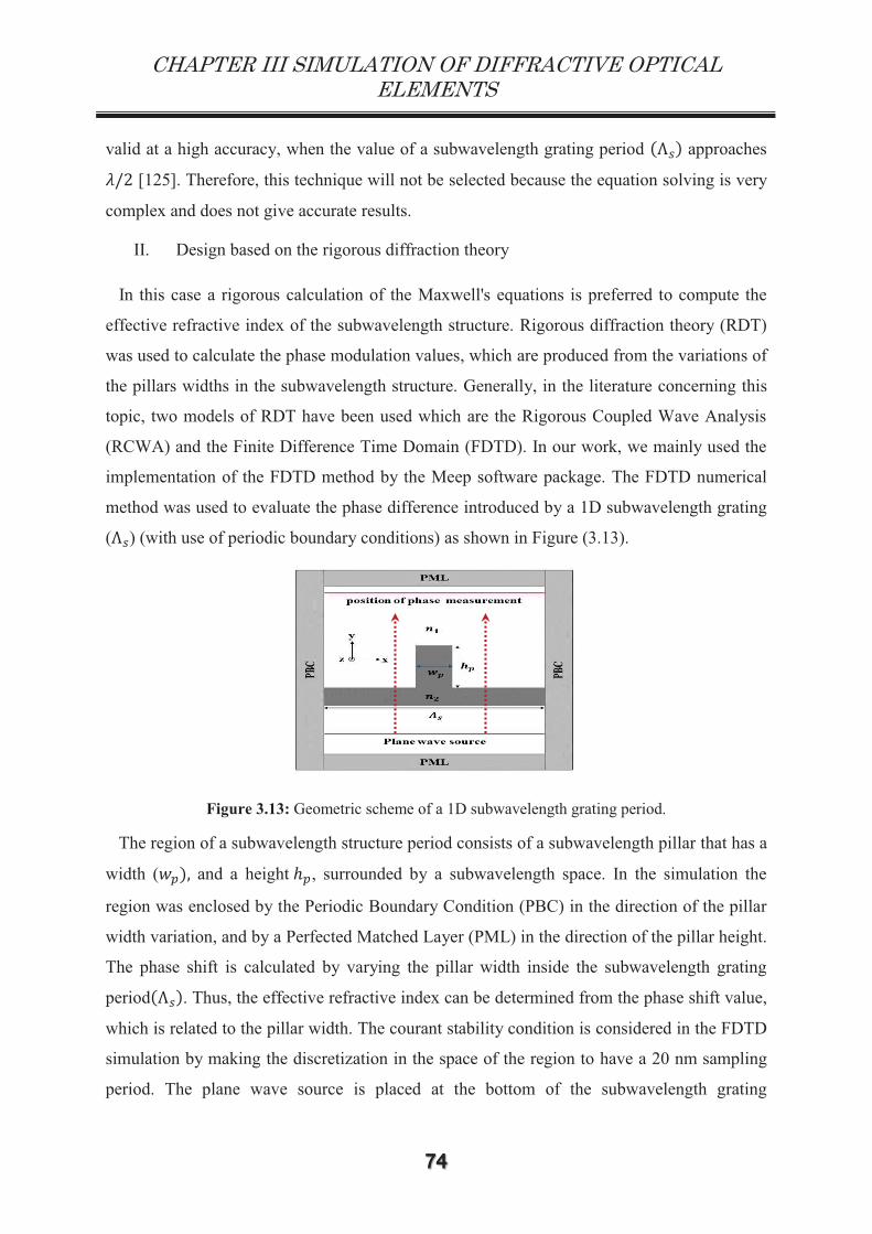
CHAPTER III SIMULATION OF DIFFRACTIVE OPTICAL ELEMENTS
�"
valid at a high accuracy, when the value of a subwavelength grating period approaches
[125]. Therefore, this technique will not be selected because the equation solving is very
complex and does not give accurate results.
II. Design based on the rigorous diffraction theory
In this case a rigorous calculation of the Maxwell's equations is preferred to compute the
effective refractive index of the subwavelength structure. Rigorous diffraction theory (RDT)
was used to calculate the phase modulation values, which are produced from the variations of
the pillars widths in the subwavelength structure. Generally, in the literature concerning this
topic, two models of RDT have been used which are the Rigorous Coupled Wave Analysis
(RCWA) and the Finite Difference Time Domain (FDTD). In our work, we mainly used the
implementation of the FDTD method by the Meep software package. The FDTD numerical
method was used to evaluate the phase difference introduced by a 1D subwavelength grating
( ) (with use of periodic boundary conditions) as shown in Figure (3.13).
Figure 3.13: Geometric scheme of a 1D subwavelength grating period.
The region of a subwavelength structure period consists of a subwavelength pillar that has a
width ( and a height , surrounded by a subwavelength space. In the simulation the
region was enclosed by the Periodic Boundary Condition (PBC) in the direction of the pillar
width variation, and by a Perfected Matched Layer (PML) in the direction of the pillar height.
The phase shift is calculated by varying the pillar width inside the subwavelength grating
period . Thus, the effective refractive index can be determined from the phase shift value,
which is related to the pillar width. The courant stability condition is considered in the FDTD
simulation by making the discretization in the space of the region to have a 20 nm sampling
period. The plane wave source is placed at the bottom of the subwavelength grating

CHAPTER III SIMULATION OF DIFFRACTIVE OPTICAL ELEMENTS
�#
period , at a distance of five wavelength units. Then, the wave propagation is excited
until the field reaches a steady state. Finally, the phase difference is calculated relative to the
reference phase of a zero width pillar, by using an average value over all width of the
subwavelength grating and for five values of wavelengths.
3.5.1 Design of Subwavelength Structure Diffractive Optical Elements (SWSDOE)
The design principle of a diffractive optical element with a subwavelength structure is
based on finding the phase shift values as a function of the fill factor values. Therefore, the
phase profile of any desired continuous or multilevel phase profile of the DOE can be
replaced by the subwavelength structure having a space variant refractive index, as this has
been illustrated previously in Figure (3.12). The multilevel DOE’s structure profile can be
replaced by the subwavelength structure profile with one or several subwavelength grating
periods. Whereas, those subwavelength grating periods achieved the same phase shift in each
phase level. Therefore, it is necessary to calculate these phase shift values for a 1D binary
subwavelength grating period , as shown in Figure (3.13). The determination of the
subwavelength grating period that is related to the main design wavelength , is
subject to the following equation[126]:
(3.20)
In each subwavelength grating period , the phase shift values range between 0 to 2π,
based on the change in the pillar width, the height of the pillar is kept constant. The
maximum phase shift value is achieved with the width of the pillar equal to the
subwavelength grating period , and the height of the pillar is defined as follows:
(3.21)
Therefore, the phase shift variation is produced just by changing the pillar width in the
subwavelength grating period . In all cases, the light incidence is normal (i.e. ) and
the subwavelength grating is surrounded by air (i.e ).
In this work, the study was performed for the TE polarization.The design wavelengths are
selected from the sunlight spectrum band (400-1100) nm, with a variation steps of 100 nm
(i.e. 400:100:1100 nm), for the reasons related to the intended application. Several
subwavelength grating periods can be determined from equation (3.20) for each main design
wavelength . Therefore, the phase shift values were calculated for several subwavelength

CHAPTER III SIMULATION OF DIFFRACTIVE OPTICAL ELEMENTS
�$
grating periods related to each main design wavelength. The values of the subwavelength
grating periods are selected to start from 100 nm up to the main design wavelength with
variations value of 50 nm (i.e. =100:50: ). The phase shift values were calculated
with variations of the pillars width in each subwavelength grating period . The width of
pillars takes several values starting from 0 up to the subwavelength grating period with a
step of 5 nm (i.e nm). Figures 3.14 and 3.15 illustrate the phase shift values for
several subwavelength grating periods related to several main design wavelengths.
Figure 3.14: The phase shift values for several subwavelength grating periods (SWGP) related to the main design wavelengths: 400,500,600,700 nm.

CHAPTER III SIMULATION OF DIFFRACTIVE OPTICAL ELEMENTS
��
Figure 3.15: The phase shift values for several subwavelength grating periods (SWGP) related to the main design wavelengths 800, 900, 1000, 1100 nm.
The optimal subwavelength grating period has been explored for each main design
wavelength. The best diffraction efficiency was selected as the criterion to determine the
optimal subwavelength grating period. The diffractive lens profile was coded with several
subwavelength grating periods for each main design wavelength. While, other design
parameters were kept constant, what include the design wavelength , the focal length ,
and the lens diameter . These lenses were designed with the lens diameters values within
(1-3) mm, and the focal length values within (50-250) mm. The subwavelength grating period
values were chosen for each main design wavelength to start from 200 nm up to the main
design wavelength with a step variation by 50 nm (i.e. =200:50: ). We neglect the
subwavelength grating periods having the values 100 nm and 150 nm due to lithography
restrictions, which will be discussed later. The diffraction efficiency is calculated for the first
diffraction order of the focal point for all the main design wavelengths. These values are
illustrated in the Table (3.3). The number of the subwavelength grating periods that produce

CHAPTER III SIMULATION OF DIFFRACTIVE OPTICAL ELEMENTS
�%
diffraction efficiencies higher than 70%, increase with increasing design wavelength. This
behavior perhaps is a result of the effect of the pillar depth which is very small related to the
short design wavelengths. The evanescent waves do not decay enough to be negligible at the
opposite boundary of the subwavelength structure that have very small pillar depth.
Therefore, these evanescent waves are reflected by the boundary, and are coupled to the
propagation waves[127]. There is another explanation for this behavior, which is linked to the
birefringence effect of a subwavelength structure. The phase shift depends on the polarization
type in the zero order subwavelength structure. Therefore, the TE polarization light is cut off
in the subwavelength structure that has the pillar width smaller than half the size of the
wavelength of the incident light. In this case only the TM polarization light can propagate
inside the subwavelength structure[128]. Furthermore, the subwavelength structures have
been recently demonstrated as having the capability to provide similarly a strong, tunable
resonant light scattering, with a very small feature size (i.e. the pillars width)[129].
Design wavelength
(nm)
Subwavelength grating (swg) period (nm)
200
250
300
350
400
450
500
550
600
650
700
750
800
850
900
950
1000
1050
1100
400
43.1
6
49.1
0
61.0
3
59.2
1
45.8
4
- - - - - - - - - - - - - -
500
54.7
9
58.7
2
60.7
2
60.9
9
62.6
3
67.7
4
61.2
5
- - - - - - - - - - - - 600
55.7
0
59.8
1
60.2
0
67.3
3
69.8
2
76.8
3
69.1
8
86.1
2
57.7
8
- - - - - - - - - -
700
62.2
9
72.8
6
72.7
8
81.6
7
72.2
0
85.1
0
73.9
8
86.7
9
80.9
0
85.3
0
64.0
1
- - - - - - - -
800
66.9
5
74.7
7
78.4
6
79.6
1
75.5
1
76.2
9
81.1
6
81.5
2
82.7
5
83.6
5
83.4
6
80.6
0
69.8
5
- - - - - -
900
66.5
2
76.4
0
74.8
0
78.6
3
78.3
5
86.2
6
84.0
4
85.8
6
81.8
7
86.6
6
83.1
8
82.1
8
82.6
4
84.7
4
68.9
5
- - - -
1000
67.3
5
73.3
8
77.8
7
82.4
9
78.8
9
87.2
8
81.1
9
85.6
6
85.5
9
88.9
5
86.2
7
89.3
1
83.8
0
81.7
1
85.9
1
82.5
6
79.4
4
- -
1100
66.1
5
70.7
3
79.4
6
81.4
6
81.6
1
87.3
0
81.2
0
86.3
7
84.9
2
86.5
0
86.7
2
88.4
9
82.5
5
84.5
0
85.2
9
86.6
6
81.7
9
79.6
4
77.0
6
Table 3.3: Diffraction efficiencies values of the diffraction Fresnel lens that are designed with the different main design wavelength and encoded by different subwavelength grating periods.

CHAPTER III SIMULATION OF DIFFRACTIVE OPTICAL ELEMENTS
�&
The optimal subwavelength grating period is illustrated in Table (3.4), which is related to
each design wavelength. The pillars widths which produce the phase shift equivalent to a 4-
level and an 8-level, were calculated for each optimal subwavelength grating period, and
listed in the Tables 3.5 and 3.6. We can see that the pillar width increases in each optimal
subwavelength period with the increase of the main design wavelength.
Design wavelength
(nm) 400 500 600 700 800 900 1000 1100
Optimal subwavelength grating period
(nm)
300 450 450 550 550 650 750 750
Table 3.4: Optimal subwavelength grating periods for each main design wavelength.
It is obvious that the behavior of the electromagnetic field propagation is different among
the multilevel and the subwavelength structure for a diffractive optical element. Therefore,
the broadband diffraction efficiency and the linear chromatic aberration will be considered
for the diffractive lens, having different profile structures. The optimal subwavelength grating
periods will be used for this study, which means they could be used for the coding of 4-level
and 8-level subwavelength structure profile
Design wavelength
(nm)
Optimal subwavelength grating period (nm)
4-level phase shift values (Rad)
The widths of pillars (nm)
0 3 /2
400 300 0 49.74 102.35 180.99 500 450 0 66.87 132.64 250.93 600 550 0 79.41 151.56 300.52 700 550 0 89.40 177.63 321.30 800 650 0 102.36 203.99 365.96 900 650 0 110.20 225.03 400.10 1000 750 0 124.38 248.13 449.86
11000 750 0 141.41 295.08 502.30 Table 3.5: The widths of the pillars produce phase shift equivalent to 4-level quantization of the
optimal subwavelength grating period related to the main design wavelength.

CHAPTER III SIMULATION OF DIFFRACTIVE OPTICAL ELEMENTS
%'
Design wavelength
(nm)
Optimal subwavelength grating period
(nm)
8-level phase shift value (Rad)
The width of pillar (nm)
0
400 300 0 26.71 49.74 74.19 102.35 135.96 180.99 241.55 500 450 0 36.91 66.87 97.46 132.46 178.14 250.93 350.91 600 550 0 45.48 79.41 111.63 151.63 206.64 300.52 429.90 700 550 0 48.47 89.34 130.68 177.63 237.72 321.30 439.32 800 650 0 55.75 102.36 150.71 203.99 269.37 365.96 521.91 900 650 0 58.71 110.20 163.21 225.03 301.62 400.10 528.17
1000 750 0 66.23 124.38 182.84 248.13 331.44 449.86 601.94 1100 750 0 71.89 141.04 214.16 295.08 389.50 502.30 629.55 Table 3.6: The width of pillars produce phase shift equivalent to an 8-level quantization of the
optimal subwavelength grating period related to the main design wavelength.
3.6 Broadband Spectrum behavior of the diffractive lens
A conventional diffractive lens shows generally large chromatic aberration and frequently a
low diffraction efficiency for the broadband spectrum. Thus, a conventional diffractive lens is
not useful for multispectral applications. The diffraction efficiency of the diffractive lens can,
in principle, be set at 100% for the design wavelength (blazed wavelength), while, it
decreases by changing the illumination wavelength. As stated previously, the focal points and
the diffraction efficiencies for the multi wavelengths are obtained by equations 3.8 and 3.9,
respectively, in a conventional diffractive lens. These equations depend on the scalar
diffraction theory, and are based on the thin element approximation. In some cases, SDT
theory becomes powerless to predict the diffractive behavior of the broadband source (i.e.
multi wavelength) of a diffractive lens. This happens when the diffractive lens has a thick
depth surface modulation profile compared to some wavelengths of the illumination source.
This effect is more noticeable when the diffractive lens is designed with a subwavelength
structure. In order to evaluate the broadband behavior of a diffractive lens, several diffractive
lenses have been designed with different design wavelength , and two types of surface
modulation depth profiles. The selected test design wavelengths are 400, 700, and 1100 nm,
which represent the values in the beginning, in the middle, and in the end of the targeted
spectrum (i.e. 400-1100 nm). The diffractive lens structure profile uses coded into 4-level,
and an equivalent as 4-level subwavelength structure profile. The illumination broadband
spectrum was selected for incorporating the wavelengths in the range between 400 nm and
1100 nm with a variation step of 50 nm. The Focal Points (FP), and the Diffraction
Efficiencies (DE), have been calculated for the broadband spectrum that illuminates the
diffractive lens. The focal points were calculated by two ways: firstly, through an analytical

CHAPTER III SIMULATION OF DIFFRACTIVE OPTICAL ELEMENTS
%�
method by using equation 3.8 which is based on the scalar diffraction theory. Secondly,
through a numerical method by using our proposed hybrid FDTD-ASM propagator which
is based on rigorous diffraction theory. As shown in Figure (3.16), the broadband spectrum
behavior of the diffractive lens is very affected by the designing parameters of the diffractive
lens. The diffractive lens was designed for the smallest wavelength of the intended spectrum
(i.e. 400 nm). The focal point behavior stays the same for the broadband spectrum that
illuminates the diffractive lens, which means for the analytical and the numerical calculations
and for both multilevel and a subwavelength structure profile. While, this behavior changes
with increases in the main design wavelength, for the diffractive lens that is designed for the
wavelength 400nm, the depth profile of the surface modulation produces a phase shift equal
to 2 only for the main design wavelength. Therefore, this depth profile is considered thin for
all the values of the broadband spectrum. The wavelengths of the broadband spectrum passed
without diffraction through the depth profile of the diffractive lens. Therefore, the SDT can
be applied by considering the thin element approximation. So the maximum of the light
power density is diffracted into a first diffraction order for all the wavelengths. For the
diffractive lenses that are designed with the main wavelengths 700 nm and 1100 nm, their
depth profiles don’t produce a phase shift equal to 2π not simply for the design wavelength,
but also for several wavelengths depending on the depth profiles. Therefore, the depth profile
cannot be considered as being thin for all the broadband spectrum. The maximum of the
lighting power density is not only diffracted into a first diffraction order for all wavelengths.
But, the light power density is distributed among the diffraction orders. This process is very
disturbed by a type of diffractive lens structure profile. We can see clearly that the
redistribution of the light power density among the diffraction orders increases for the higher
design wavelengths values of the targeted light spectrum. The distribution of the light power
density depends on the harmonic degree[71] of the diffractive lens depth profile relative to
the particular illumination wavelength. when the diffractive lens depth profile is equal to, or
close to a second or third harmonic degree for some illumination wavelengths of the
broadband spectrum. These wavelengths are diffracted into a second or a third diffraction
order.

CHAPTER III SIMULATION OF DIFFRACTIVE OPTICAL ELEMENTS
%
-a- -b- Figure 3.16: Broadband spectrum behavior for diffractive lenses designed with different main design
wavelengths and two structures profiles: A 4-level quantized structure profile and a 4-level subwavelength structure profile.
a- Focal point behavior, Focal Point Analytical (FPA), Focal Point Numerical for Multilevel structure profile (FPN-ML), Focal Point Numerical for SubWavelength structure profile
(FPN-SW). b- Diffraction Efficiency behavior, Diffractive Efficiency for Multilevel (DE-ML) structure
profile, Diffractive Efficiency for SubWavelength (DE-SW) structure profile. This behavior is also affected by the type of diffractive lens surface modulation depth profile
structure, as shown in Figure (3.17). The illumination wavelengths (i.e. 400, 700 ,1100 nm) are
diffracted into a first diffraction order by the diffractive lens that is designed with the main

CHAPTER III SIMULATION OF DIFFRACTIVE OPTICAL ELEMENTS
%!
wavelength 400 nm and for both structure profiles (i.e. Multilevel and subwavelength). These
wavelengths diffracted into a first diffraction order by the diffractive lens that has a subwavelength
structure profile and that is designed with the main wavelength 700 nm. While, the wavelength 400
nm is diffracted into a second diffraction order by the same diffractive lens that has a multilevel
structure profile. The diffractive lens that was designed with the main wavelength 1100 nm produced
a more complex behavior.The wavelengths 700 and 1100 nm were diffracted into a first diffraction
order by the diffractive lens that has a multilevel structure profile. Whereas, the wavelength 400 nm
is diffracted into a third diffraction order by the same lens. While, both of the wavelengths 400 and
700 nm were diffracted into a second diffraction order by the same lens, but that has a subwavelength
structure profile.
The diffraction efficiency behavior for the broadband spectrum is the same generally for the
diffractive lens that is designed with a multilevel or a subwavelength structure profile, as shown in
Figure (3.16-b). As stated previously, this behavior is subjected to equation 3.9. For the diffractive
lens designed with the wavelength 400nm, the diffraction efficiency of the broadband spectrum that is
produced by a multilevel structure profile is higher compared to to one produced by a subwavelength
structure profile. For the diffractive lens designed with the wavelengths 700 nm and 1100 nm, the
diffraction efficiency of the broadband spectrum is similar for the long wavelength in both a
multilevel and a subwavelength structure profile. While, the diffraction efficiency produced by the
diffractive lens that is designed with the wavelength 400 nm and a subwavelength structure profile
will be less for the short wavelengths compared to a multi level structure profile. For the lens
designed with the wavelength 1100 nm, the diffraction efficiency produced by the diffractive lens that
has a subwavelength structure profile will be greater for a short wavelengths compared to a multi
level structure profile. We can conclude that the design parameters of the diffractive lens have an
important effect on the behavior of this lens for the broadband spectrum. Consequently,it is possible
to design a diffractive lens having optimal parameters based on this simple knowledge. Thereafter,
this lens can achieve an acceptable performance for both the diffraction efficiency and the linear
chromatic aberration for a specific spectrum band and can be used for certain applications.

CHAPTER III SIMULATION OF DIFFRACTIVE OPTICAL ELEMENTS
%"
-a- -b- Figure 3.17: Focal point behavior produced by the diffractive lenses that were designed for different
main wavelengths and two structure profiles for three illumination wavelengths. a- Diffractive lens coded into a 4-level quantized structure profile.
b- Diffractive lens coded into a 4-level subwavelength structure profile.

CHAPTER III SIMULATION OF DIFFRACTIVE OPTICAL ELEMENTS
%#
3.7 Conclusion
In conclusion, a diffraction grating and a diffractive lens can be used to perform some
useful functions for solar cell applications, as stated previously in chapter 1. The hybrid
FDTD-ASM propagator proposed provides the advantage to overcome the limitations of both
of the diffraction theories (SDT and RDT). It can be used to accurately simulate the
diffraction behavior of the electromagnetic field from a big size of DOE in the acceptable
range compatible with the limits of FDTD simulation, and different structure profile of a
DOE. In addition, we can use this propagator to simulate the behavior at a large propagation
distance with reasonable computational resources consumption. The EMT can be also used
with the RDT for the design of a DOE that has a subwavelength structure profile as we
propose. The diffractive lens can be designed with an optimal subwavelength grating period
to achieve higher diffraction efficiency. The number of optimal subwavelength grating
periods increases for the longest main design wavelength. The broadband spectrum behavior
of a diffractive lens has been studied to regard of their design parameters. We discovered that
some design parameters of a diffractive lens play an important role in the behavior of lenses
having to process a broadband spectrum. The diffraction efficiency and the focal point, which
is related to the linear chromatic aberration, have been studied with respect to its design
parameters. Finally, we can conclude that a diffractive lens can be designed with optimal
design parameters (i.e. design wavelength and type of the structure profile) to achieve better
performance to process conveniently light on a broadband. This performance includes the
purpose of implementing an optical function that can be exploited for solar cell applications.
The broadband diffraction efficiency and the linear chromatic aberration will be controlled
through a selection of the optimal parameters for the design. In the next chapter, this
knowledge will be exploited to design a diffractive optical element that can provide the
optical functions of both spectrum splitting and beam concentration of sunlight for the PV
cell application.

CHAPTER IV DIFFRACTIVE OPTICAL ELEMENT PROPOSED MODEL FOR PV CELLS APPLICATIONS
%$
4.1 Introduction
In this chapter, we will provide the working principle of the diffractive optical element that
we propose to achieve optical functions for PV cells applications. As stated previously in
chapter 1, our aim is to design a diffractive optical element that provides simultaneously the
optical functions of the spectrum splitting and the beam concentration (SSBC) of the sunlight
for third generation PV cells. This topic has been introduced previously with a review on the
literature of this subject. Some diffractive optical elements such as diffraction gratings and
diffractive lenses, have been used to implement the optical functions of the spectrum splitting
and the beam concentration (SSBC) of the sunlight, respectively. In some cases, hybrid
diffractive optical elements were designed to achieve more or less these optical functions. In
our case a hybrid diffractive optical element structure profile is produced by merging the
diffraction grating structure profile with the diffractive lens structure profile. We will explain
the possibilities and the limitations of using hybrid diffractive optical elements to implement
advanced optical functions for PV cell applications. Finally, we will present an original
diffractive optical element (an off-axis diffractive lens) that can be used to implement the
SSBC for the PV cells of the third generation.
4.2 Working principle of a DOE for the PV cell applications
In this section, we will present the working principle of DOE's that were proposed to
implement the targeted optical functions for PV cell applications. The main working principle
depends on the passive properties of the diffractive optical elements. It is known that the
diffractive optical elements are characterized by a high achromatic aberration. As stated
previously in chapter 3, for example, a diffractive lens concentrates wavelengths of the
broadband light into several focal points, in accordance with the general principle of
achromatic aberration. Therefore, the focal points for each wavelength are dependent on the
design wavelength of the DOE through the equation that follows:
(4.1)
This equation was mentioned in chapter 3 under number (3.8), and is rewritten again here as a
reminder.

CHAPTER IV DIFFRACTIVE OPTICAL ELEMENT PROPOSED MODEL FOR PV CELLS APPLICATIONS
%�
Figure (4.1) illustrates the schematic diagram that depicts the working principle of a DOE
proposed for achieving simultaneously the spectrum splitting and the beam concentration of
the sunlight. The broadband spectrum of the sunlight arrives at a normal angle on the front of
the DOE, it will be concentrated into multi focal points corresponding to each wavelength.
The proposed DOE device was designed to focus the wavelengths of the broadband spectrum
on the line vertically on one edge of the DOE structure profile.
Figure 4.1: Schematic diagram of the DOE device implementing the functions of spectrum splitting and beam concentration simultaneously.
The wavelengths represent the beginning , the separation and the end of the
intended broadband spectrum that will be focused at respectively.
Consequently, the broadband spectrum will be separated into two bands. The band1 contains
the wavelengths between , which will be focused at a lateral distance
between . While, band2 contains the wavelengths between , which will be
focused at the lateral distance between . Therefore, two different PV cells can be
placed in the position of the focal point for the separated wavelength (FS), on either side of
the optical axis which is vertical on the DOE edge. The light power density (LPD) for the
wavelengths of band1 will be absorbed and converted into electricity by PV1 cell after
passing their expected focal point, which are located between FS and Fe. While, the light
power density for the wavelengths of band2 will be absorbed and converted into electricity by
PV2 cell before arriving their expected focal point, which are located between Fb and Fs . In
this manner, the proposed DOE can achieve the spectrum splitting and the beam
concentration simultaneously.

CHAPTER IV DIFFRACTIVE OPTICAL ELEMENT PROPOSED MODEL FOR PV CELLS APPLICATIONS
%%
The performance of the proposed hybrid device will be defined in the same manner as for a
solar cell concentrator, with modifications that fit the intended specific functionalities. As
stated previously in chapter 1, three parameters have been used to evaluate the performance
of a solar cell concentrator.
i. The geometrical concentration factor which is the ratio between the area of
the collector surface (i.e. concentrator) and the area of the receiver surface
(i.e. PV cell).
ii. The optical efficiency factor which is defined as the ratio between the flux
absorbed by the PV cell and the flux collected by the concentrator.
iii. The optical concentration factor which is defined by the multiplication of
with , as defined in the equation that follows:
(4.2)
Therefore, a new formula for the optical concentration factor must be derived in order to
evaluate the performance of the proposed device. The diffraction efficiency must be
calculated for each wavelength, in accordance with the working principle of the proposed
DOE. Therefore, the optical efficiency factor for each band will be calculated by taking the
average of the diffraction efficiency for all the wavelengths. The new formula of the optical
efficiency factor can be written as follows:
(4.3)
Where k is the number of wavelengths in the spectrum band.
The final formula for the optical concentration factor for the proposed device can be written
as follows:
(4.4)
The methodology that was adopted to calculate the optimal bandwidth for a PV cell using our
proposed device depends on the Linear Chromatic Aberration (LCA) effect. The LCA for the
different wavelengths out of the DOE is defined as follows[130]:

CHAPTER IV DIFFRACTIVE OPTICAL ELEMENT PROPOSED MODEL FOR PV CELLS APPLICATIONS
%&
(4.5)
Therefore, the width of each PV cell can be calculated depending on the LCA by considering
the extreme wavelengths of each band, as show in Figure (4.2), and from the following
equations:
(4.6)
(4.7)
There are two main tasks that must be achieved in order to obtain the optimal performance.
Firstly, the linear chromatic aberration must be reduced to increase the concentration. This
allows a reduction of the lateral distance between the focal points for the extreme
wavelengths of each band. Secondly, the optical efficiency factor must be increased for each
band.
PV1 cell PV2 cell
Figure 4.2: Schematic diagrams that represent the calculation methodology for the optimal widths of the PV cells.
The specific properties of the diffraction grating and the diffractive lens, that have a
multilevel and a subwavelength structure profile, will be exploited to implement optimal
performance. Finally, there is another schematic diagram that can be used to describe the
working principle of the device proposed. In this diagram, two similar DOE's are arranged
with an opposite orientation with an opaque barrier included. The width of this opaque barrier
is equal to the width of PV2 cell ( . Thus, the incident sunlight will be normally guided
into three PV cells, as shown in Figure (4.3). Two of those PV cells are similar and each PV

CHAPTER IV DIFFRACTIVE OPTICAL ELEMENT PROPOSED MODEL FOR PV CELLS APPLICATIONS
��
cell will receive the light of band 2 that will be concentrated by a part of DOE in alignment
with it. While, the other PV cell will receive the light of band2 from both parts of the DOE
device.
Figure 4.3: Schematic diagram of the DOE device implementing the functions of spectrum splitting and beam concentration simultaneously for three PV cell.
In the next paragraphs, this model will be validated through the description of two optical
devices that can be used with the same working principle.
4.3 G-Fresnel
The G-Fresnel is the first optical device that can be used to achieve the working principle of
the proposed model. A G-Fresnel is a planar hybrid diffractive optical element that is
obtained by merging the profiles of both of the diffraction grating and the Fresnel lens into a
single profile. The term G-Fresnel is derived from a shortcut (Grating+Fresnel lens) and has
been used first by Chuan Yang [131, 132]. A G-Fresnel device has been shown to integrate
the functions of a grating and a Fresnel lens into a single hybrid device. Thus, the optical
functions of the spectrum splitting and the beam splitting have been obtained simultaneously
by a single optical device. This device was proposed for a planar miniature optical
spectrometer that can be used in optofluidic applications. This idea was exploited by Ye Jia-
Sheng et al [11, 68] and Céline Michel et al [67]through merging a Diffractive Grating (DG)
with a Diffractive Lens (DL) or a Refractive Lens (RL) for PV cell applications. A G-Fresnel
can be implemented with two forms of the structural profiles:

CHAPTER IV DIFFRACTIVE OPTICAL ELEMENT PROPOSED MODEL FOR PV CELLS APPLICATIONS
�
I. The grating structure profile and either the refractive Fresnel lens or the diffractive
lens structure profile, are placed separately on opposite sides (double sided) of the G-
Fresnel device, as shown in Figure (4.4-a).
II. The grating structure profile and either the refractive Fresnel lens or the diffractive
lens structure profile, are integrated in one side (single sided) of the G-Fresnel device,
as shown in Figure (4.4-b).
Grating structure profile +
Grating structure profile +
Refractive Fresnel lens or
Diffractive lens structure profile =
Refractive Fresnel lens or
Diffractive lens structure profile =
G-Fresnel structure profile
-a-
G-Fresnel structure profile
-b-
Figure 4.4: Scheme of the G-Fresnel structures profiles. a- Double sided G-Fresnel structure profile. b- Single sided G-Fresnel structure profile.
Chuan Yang used polydimethylsiloxane (PDMS) and a soft lithography technique for the
fabrication of a G-Fresnel device with a double sided structure profile. We will explore the
possibility to design a G-Fresnel device with a single sided structure profile, which is
produced by merging the diffraction grating with the diffraction lens. The maximum depth
profile of both the diffraction grating ( ) and the diffraction lens ( ) are defined as
follows:
(4.8)
(4.9)

CHAPTER IV DIFFRACTIVE OPTICAL ELEMENT PROPOSED MODEL FOR PV CELLS APPLICATIONS
�!
Where is the wave number, is the design wavelength, n is the refractive index
of substrate, and is the maximum phase shift (i.e. 2 ) produced by the depth profile for the
design wavelength. The maximal depth profile of a G-Fresnel ( is defined as follows:
(4.10)
Some conditions must be considered in the process of designing a G-Fresnel device.
Firstly, a maximum depth profile must be chosen to produce a phase shift equal to 2π for the
design wavelength, in both the diffraction grating and the diffraction lens. Consequently, a G-
Fresnel depth profile will produce a maximum phase shift equal to 4 for the design
wavelength. As we know from the basic working principle of the DOE, there is no change in
the performance of the DOE with an increase or decrease of its depth profile. This means, the
additional thickness of DOE profile that produces a multiple of 2π a phase shift value will
achieve the same performance of the DOE profile that has 2π a phase shift value. We prefer
to design a G-Fresnel depth profile that produces a maximum phase shift equal to 2 .
Therefore, in this case, a G-Fresnel profile will be equivalent to an off-axis lens profile with
its center shifted to xc, as shown in Figure (4.5).
This center of an off-axis lens depends on the design parameters of the diffractive grating and
of the diffractive lens, and is defined by the following equation:
(4.11)
Where F is the focal length of the diffractive lens and is the grating period of the diffraction
grating. The main advantage of the design of a G-Fresnel with a single sided depth profile, is
the possibility to fabricate it by conventional lithography techniques. Secondly, as stated
previously in the paragraph that explains the working principle of the proposed DOE, the
intended function of a SSBC can be implemented when the light is focused on the optical
axis, which is orthogonal to the edge of the DOE. Therefore, the design parameters of the G-
Fresnel must be optimized to ensure that the center of an off-axis element will be on the edge
(i.e. xc is equal to the width of a G-Fresnel device), as shown in Figure (4.5-c). Thirdly, the
angle of the grating period which is known as the blaze angle ) must be optimized to
achieve a high diffraction efficiency. We will study in the next paragraphs the effect of
structure type on the performance of a G-Fresnel device.

CHAPTER IV DIFFRACTIVE OPTICAL ELEMENT PROPOSED MODEL FOR PV CELLS APPLICATIONS
�"
-a- -b- -c-
Figure 4.5: Scheme of the possible G-Fresnel structures profiles. a- Single sided G-Fresnel structure profile that produces a phase shift of 4 .
b- Single sided G-Fresnel structure profile, such as an Off-axis lens structure profile that produces phase shift of 2 .
c- Single sided G-Fresnel structure profile, such as an Off-axis lens structure profile with the center xc
that will be in the edge.
4.3.1 G-Fresnel performance with a multilevel structure profile
The G-Fresnel device performance is investigated with respect to the ability to implement
the intended SSBC function. A G-Fresnel device was designed with a single sided G-Fresnel
structure profile such as an off-axis Fresnel lens structure profile. Furthermore, some design
parameters were subjected to the optimization process. As stated previously in chapter 3, the
design wavelength of the diffractive lens has an important effect on the diffraction
efficiency for a broadband spectrum. In addition, the blaze angle of the diffraction
grating has a similar effect for the broadband spectrum. Therefore, these two parameters are
optimized in the design process of a G-Fresnel device. In this manner, we can set the optimal
structure profile that can be used for the targeted application. The G-Fresnel structure profile
is quantized into 8-levels. The solar spectrum considered is in the range of 400-1100 nm,
which is chosen for the PV cell applications. The goal is to separate this spectrum into two
bands; band1 contains all the wavelengths between 400-800 nm. While, band2 contains all the
wavelengths between 800-1100 nm. These two bands can be converted into electrical energy
by a pair of PV cells, which are for instance copper indium gallium selenide (CIGS) cells that
have a low-band-gap 1.05 eV, as well as Si/GaAs cells, that have a high-band-gap 1.5 eV.
The strategy that will be adopted in the design of a G-Fresnel device depends on the different
design conditions. Firstly, the design wavelengths will be selected at the beginning, in the
middle and at the end of the targeted spectrum (i.e. 400 nm, 700 nm, and 1100 nm).
Secondly, the designed focal length of the diffractive lens and the grating period of the
diffraction grating will be selected to achieve two things;

CHAPTER IV DIFFRACTIVE OPTICAL ELEMENT PROPOSED MODEL FOR PV CELLS APPLICATIONS
�#
i. The center of an off-axis lens from a G-Fresnel device profile must be located at
the edge to provide the condition required for the targeted function (i.e. SSBC).
ii. The blaze angle ( of the diffraction grating must be equal or less than 5o, to ensure
that a high diffraction efficiency is obtained for the broadband spectrum.
G-Fresnel devices were obtained by merging the diffractive lenses and the diffraction
gratings that have the design parameters shown in Table (4.1).
Design parameters G-Fresnel1 G-Fresnel2 G-Fresnel3 G-Fresnel4
DL DG DL DG DL DG DL DG
Design wavelength (nm) 400 400 700 1100
Design focal length (mm)
25 - 25 - 14.2857 - 18.1818 -
Diameter D (mm) 1
Pixel size (µm) 1
Harmonic degree p 1 - 2 - 1 - 1 - Refractive index n 1.46
Grating period (µm) - 20 - 20 - 40 - 20
Blaze angle - 2.4896 - 2.4896 - 4.3511 - 3.4212 Separation distance
(mm) 12.5 12.5 12.5 25
Table 4.1: The design parameters of different G-Fresnel devices, that have a multilevel structure profile.
The focal points, and the diffraction efficiency, for the broadband spectrum represent the
most important factors, in evaluation the validity of the proposed device. These parameters
have been studied for the intended spectrum with sampling step 10 nm (i.e. 400:10:1100
nm). The focal points behavior study provides the information necessary about the linear
chromatic aberrations, and the beam concentration ability of the proposed device. Thus , the
width of each PV cell is determined as well as the geometrical concentration factor
.The focal points that were calculated are based on two methods:
i. The analytical method by using equation 4.1, that depends on scalar diffraction
theory.
ii. The numerical method by using an hybrid FDTD-ASM propagator, that depends on
both scalar diffraction theory and rigorous diffraction theory.

CHAPTER IV DIFFRACTIVE OPTICAL ELEMENT PROPOSED MODEL FOR PV CELLS APPLICATIONS
�$
As stated in chapter 3, the design wavelength and the harmonic degree have an
important effect on the focal points of the broadband spectrum. Figure (4.6) illustrates the
focal points of G-Fresnel devices that were designed with different parameters. A G-Fresnel 1
designed with and shows that all the light power of the wavelengths
focuses in the 1st diffraction order. The behavior of the focal points is as when calculated by
both methods (analytical and numerical). While, a G-Fresnel2 designed with
and shows a different behavior. The focal points values were calculated in an
analytical way using equation (4.1) for this lens with a second harmonic degree. Thus, these
values are doubled compared to the values calculated at the first diffraction order of lens has
the first harmonic degree. While, the numerical calculation by using the proposed propagator
(FDTD-ASM) shows a different behavior compared to the analytical method. The light
power density is mostly focused on the 4th diffraction order for the wavelengths between 400-
560 nm and is mostly focused on the 2nd diffraction order for the remaining wavelength of the
targeted spectrum.
G-Fresnel1 G-Fresnel2
G-Fresnel3 G-Fresnel4
Figure 4.6: The focal points for the broadband spectrum produced from a G-Fresnel designed with different parameters and a multilevel structure profile.

CHAPTER IV DIFFRACTIVE OPTICAL ELEMENT PROPOSED MODEL FOR PV CELLS APPLICATIONS
�%
The G –Fresnel3 and G-Fresnel4 designed with nm and nm with p=1,
respectively, produced the same behavior as a G-Fresnel 2. The analytical calculation method
predicts the light power of the wavelengths that is mostly focused on the 1st diffraction order.
While the numerical calculation method predicts exactly the light power of the wavelengths,
that is focused in different diffraction orders. In the case of the G-Fresnel 3, the light power
of wavelengths between 400-500 nm is mostly focused on the 2nd diffraction order. While it
is mostly focused at the 1st diffraction order for the remaining wavelengths from the targeted
sunlight spectrum. In the case of the G-Fresnel 4, the light power of the wavelengths among
400-470 nm is mostly focused on 3th diffraction order, the wavelengths between 475-730 nm,
is mostly focused on the 2nd diffraction order. While, it is mostly focused on the 1st diffraction
order for the remaining wavelengths of the targeted spectrum. This behavior is produced
because the depth profile of a G-Fresnel is “thick” for these wavelengths. In this way, these
illumination wavelengths acquire the phase shift having a value above 2π through the passage
in a G-Fresnel structure profile. The width of each PV cell is calculated depending on
the hypothesis illustrated in Figure 4.2, and by using equations (4.6) and (4.7). Therefore, the
geometrical concentration factor can be determined for each G –Fresnel. We found that some
modifications happen to this hypothesis in some cases. The calculation of the width of the PV
cell depends on the focal points of the extreme wavelengths of each separated band. In
the case of the G-Fresnel 1, this relation can be applied because the focal point of is
higher than the focal point of . While, for the other G-Fresnel, this relation will not be
valid because the focal point of is smaller than the focal point of , for the reasons
aforementioned. Therefore, the width of a PV1 cell will be calculated relatively to the
wavelength that will focus far from the focal point of . The optical efficiency was
calculated for the intended light spectrum on both two surfaces of the PV cells, and for G-
Fresnel devices designed as shown in Figure (4.5). For a G-Fresnel 1 a high diffraction
efficiency more than 70 % can be reached, for all wavelengths of the band1, that focus at the
PV1 cell (i.e. While, the average diffraction efficiency is about 40 % for the light
power of all wavelengths of the band1, that focus onto the PV2 cell (i.e. ). The optical
efficiency is less than 30 % for all wavelengths of the band2 that focus at a PV2 cell. While, it
is less than 10 % for the light power of all wavelengths of the band2 that focus at the PV1 cell.
This means this G-Fresnel achieves a high value of the in only a single PV cell (i.e. PV1
cell), with a low value of the . For another PV cell (i.e. PV2 cell), a low value of the

CHAPTER IV DIFFRACTIVE OPTICAL ELEMENT PROPOSED MODEL FOR PV CELLS APPLICATIONS
�&
will go with a high value of the , as shown in Table (4.2). A G-Fresnel 2 achieves
relatively identical values of the for both PV cells, but the is higher in a PV2 cell
compared to a PV1 cell. A G-Fresnel 3 achieves the same behavior of the as a G-Fresnel
2, but the is relatively identical for both PV cells, this means that the difference is low.
A G-Fresnel 4 achieves an opposite behavior compared to G-Fresnel 1. The higher is
achieved in the PV1 cell, with a low value of the , and the low is achieved in the
PV2 cell of with a high value of the .
Figure 4.7: The optical efficiency rigorously calculated using FDTD-ASM propagator at each PV cell surface which is produced from the G-Fresnel devices designed with different parameters and a
multilevel structure profile.
We can see clearly, the best performance was obtained for both the and the for the
case of G-Fresnel 3 and G-Fresnel 2.

CHAPTER IV DIFFRACTIVE OPTICAL ELEMENT PROPOSED MODEL FOR PV CELLS APPLICATIONS
�'
G-Fresnel
type
Band1 400-800 nm
PV1 cell Band2 800-1100 nm
PV2 cell
(mm)
(mm)
G-Fresnel1 0.52 1.12 80.00 41.63 121.6 0.333 3.0 20.60 3.78 61.80
G-Fresnel2 0.2941 3.40 47.11 4.85 160.17 0.333 3.0 84.27 36.62 240.81
G-Fresnel3 0.3684 2.71 63.63 9.09 171.54 0.333 3.0 72.66 26.32 217.98
G-Fresnel4 0.28 13.50 14.16 5.80 191.16 0.280 3.6 78.97 36.97 284.92
Table 4.2: The values of the factors that describe the performance of the SSBC for the proposed device, that are the G-Fresnel devices designed with different parameters and a multilevel structure
profile.
4.3.2 G-Fresnel performance with a subwavelength structure profile
The performance of a G-Fresnel device that have a subwavelength structure will now be
investigated with respect to its ability to perform spectrum splitting and beam concentration
simultaneously of sunlight. The same conditions will be adopted for the design parameters of
a G-Fresnel device, as aforementioned in the last paragraph. In addition, the same spectrum
will be chosen for the study of the performance of this G-Fresnel. The designed G-Fresnel
device will be coded with a two different subwavelength structures profiles, that are
equivalent to 4-level and 8-level quantized structures profiles. The designed parameters of the
G-Fresnel devices are presented in Table (4.3).
Design parameters G-Fresnel 1 G-Fresnel 2
DL DG DL DG Design wavelength
(µm) 400 700
Design focal length (mm)
42.25 - 17.286 -
Diameter D (mm)
1.3 1.1
Subwavelength grating period (nm)
650 550
Harmonic degree p 2 - 1 -
Refractive index n 1.46 Grating period
(µm) - 26 - 22
Blaze angle - 1.9155 - 3.9568
Separation distance (mm)
21 15
Table 4.3: Design parameters of different G-Fresnel devices, that have a subwavelength structure profile.
These design parameters are selected for the purpose to achieve a high value of both the
geometrical concentration factor and the optical efficiency factor for both of

CHAPTER IV DIFFRACTIVE OPTICAL ELEMENT PROPOSED MODEL FOR PV CELLS APPLICATIONS
��
the light bands separated. Therefore, the design wavelengths have been chosen to be 400 nm
with a 2nd harmonic degree for a G-Fresnel1 and 700 nm with a 1st harmonic degree for a G-
Fresnel 2. These design parameters provided the intended goal of the G-Fresnel devices that
have a multilevel structure profile. A G-Fresnel1 is designed with 2nd harmonic degree;
consequently its depth profile will provide a phase shift. Therefore, the illumination
wavelength of 800 nm acquires a 2π phase shift through a passage in a G-Fresnel1 structure
profile. The subwavelength grating period was chosen for each G-Fresnel device that
corresponds to the wavelength which acquires a 2 phase shift through its passage in this
profile structure. As stated in chapter 3, the optimal subwavelength grating periods are
650 and 550 nm for the wavelength 800 and 700 nm, respectively. The widths of pillars are
presented in Table (4.4) for these optimal , that are equivalent to 4-level and 8-level
quantized structures profiles.
N-Level
Subwavelength grating period (nm) 650 550
Phase (360o)
Pillar width (nm)
Phase (360o)
Pillar width (nm)
4-level
0 0 0 0 90 102.36 90 89.40 180 203.99 180 177.63 270 365.96 270 321.30
8-level
0 0 0 0 45 55.75 45 48.47 90 102.36 90 89.34 135 150.71 135 130.68 180 203.99 180 177.63 225 269.37 225 237.72 270 365.96 270 321.30 315 521.91 315 439.32
Table 4.4: Widths of the pillars in a subwavelength grating period ) that are equivalent to N-levels.
The behavior of the focal points does not change by increasing a subwavelength encoding
from 4-level to 8-level for both G-Fresnel, as shown in Figure (4.8). This behavior generally
seems identical for a G-Fresnel device that has the same design parameters, and is encoded
with different techniques (i.e. a multilevel and a subwavelength profile). The only difference
observed is that the light power of the short wavelengths is mostly focused on the same
diffraction order, as it is the case for a majority of the wavelengths of the targeted spectrum.
Therefore, the is decreased in both PV cells. The one produced from a subwavelength
profile can be compared to a multilevel profile.

CHAPTER IV DIFFRACTIVE OPTICAL ELEMENT PROPOSED MODEL FOR PV CELLS APPLICATIONS
���
G-Fresnel1 G-Fresnel2
Figure 4.8: Focal points for a broadband spectrum produced from a G-Fresnel that is designed with different parameters and a subwavelength structure profile.
The optical efficiency is illustrated in Figure 4.9 on both PV cells and for G-Fresnel devices
designed. The G-Fresnel1 shows an increase in the optical efficiency for the light power of all
wavelengths of the band1, which are concentrated on the PV1 cell (i.e. . This can be
compared to another model of a G- Fresnel that is coded with a multilevel structure profile. It
shows a decrease of the optical efficiency for the light power of all the wavelengths of the
band1 that are concentrated on the PV2 cell (i.e. ). This performance improves for a
G-Fresnel that is encoded with an 8-level subwavelength structure profile. The G-Fresnel2
shows linear performance compared to that of a device coded with a multilevel structure. The
only difference observed is a reduction of the light power of all the wavelengths of the band1,
that are concentrated on the PV2 cell (i.e. ). The advantage of an 8-level
subwavelength encoding is an increase in the light power of all wavelengths of the band2, that
focus on the PV2 cell (i.e. of this G-Fresnel device.
The performance of these G-Fresnel devices is illustrated in Table (4.5), which is related to
the implementation of the functions of the spectrum splitting and beam concentration.

CHAPTER IV DIFFRACTIVE OPTICAL ELEMENT PROPOSED MODEL FOR PV CELLS APPLICATIONS
���
Figure 4.9: The optical efficiency rigorously calculated using FDTD-ASM propagator at each PV cell surface which is produced from the G-Fresnel devices designed with different parameters and a
subwavelength structure profile.
G-Fresnel type
Band1 400-800 nm PV1 cell
Band2 800-1100 nm PV2 cell
(mm)
(mm)
G-Fresnel1
4-level subwavelength
0.65 2 51.70 9.99 103.40 0.52 2.5 73.30 16.35 183.25
G-Fresnel1 8-level
subwavelength 0.65 2 59.28 9.99 118.56 0.52 2.5 78.31 13.67 195.77
G-Fresnel2 4-level
subwavelength 0.55 2 63.51 17.74 127.02 0.4 2.75 56.17 10.28 154.46
G-Fresnel2 8-level
subwavelength 0.55 2 62.73 13.32 125.46 0.4 2.75 67.08 13.08 185.13
Table 4.5: Values of the factors that describe the performance of the SSBC for the proposed devices: G-Fresnel devices designed with different parameters and a subwavelength structure profile.

CHAPTER IV DIFFRACTIVE OPTICAL ELEMENT PROPOSED MODEL FOR PV CELLS APPLICATIONS
��
As we expect a G- Fresnel device can be implemented with specific design parameters to
achieve the working principle of the proposed model with a good performance. This means
the highest values can be obtained of both the geometrical concentration factor and the
optical efficiency factor for the both separated bands. In the next paragraph, we will
present the second optical device.
4.4 OFF-axis lens
An alternative model of an off axis lens can be used instead of a G-Fresnel device to
achieve simultaneously the functions of spectrum splitting and beam concentration (SSBC) of
sunlight. In this manner, the targeted function (i.e. SSBC) will be performed by using only
one diffractive optical element. As stated in chapter 3, in the paragraph that describes the
diffractive Fresnel lens, the diffractive Fresnel lens phase profile can be obtained through the
reduction of the phase function of the refractive lens to 2π. The depth profile of the refractive
lens (i.e. thickness of the refractive lens ) which is equivalent to roughly a thousand 2π
phase shifts, can be defined as follows:
(4.12)
Where R is the radius of curvature of the lens, is the center of the lens, and r is the radius
of the lens. Therefore, the diffractive lens depth profile (i.e. thickness of the diffractive
lens ) which produced a phase shift equal to 2 , can be defined as:
=mod( ) (3.9)
Where is the maximum thickness that produces a phase shift equal to 2 related to the
design wavelength . The center of the lens has been chosen to be equal to the lens radius
(i.e . Thus, the designed lens will achieve the necessary requirements to implement
the SSBC simultaneously. The performance of an off-axis lens will be studied for
implementing the SSBC of the intended spectrum (i.e. 400-1100 nm). The intended spectrum
will be separated into two bands: the band1 contains the wavelengths between 400-800nm
and the band2 contains the wavelengths between 800-1100 nm. The performance will be
explored for the intended spectrum with a step variation of 5 nm (i.e. 400:5:1100 nm).
4.4.1 Off-axis diffractive lens performance with a multilevel structure profile
The validation of the model proposed to achieve the SSBC, will be tested for off-axis lenses
that are coded with a multilevel structure profile. The diffractive lens has been designed with
the different optimal design parameters: the design wavelength ( ), the focal length ( ),

CHAPTER IV DIFFRACTIVE OPTICAL ELEMENT PROPOSED MODEL FOR PV CELLS APPLICATIONS
��!
the harmonic degree (p), and for two different usual materials used in the DOE fabrication
with the lithographic techniques. The design parameters of an off-axis lens are illustrated in
Table (4.6). The lenses designed were coded with an 8-level quantized structure profile.
Off-axis lens type
Design wavelength
(nm)
Focal length
(cm)
Lens diameter
D (cm)
Harmonic degree
p
Pixel Size
(µm)
Refractive index
n
Separation distance
(cm)
Off-axis lens1
350
22.8585
1
2
1 1.46
10
Off-axis lens2
2
Off-axis lens3
1
1.64
Off-axis
lens4 2
Table 4.6: Design parameters of different off axis lenses, that have different harmonic degree with a multilevel structure profile.
Several goals have been adopted through the selection of the design parameters. Firstly,
from a design viewpoint. The aim is to achieve a high performance of the geometrical
concentration factor and the optical efficiency factor .Therefore, it is necessary
to fulfil two conditions: first, the linear chromatic aberration (LCA) must be reduced among
the extreme wavelengths of each separate band to increase the . Second, the optical must
be kept high enough for all the wavelengths in each separate band, to ensure an increase of
the It was demonstrated with the case of a G-Fresnel design, that the design wavelength
and the harmonic degree have an important effect on the performance of the SSBC.
Secondly, from a fabrication viewpoint, the design parameters must be selected to ensure that
the smallest Fresnel zone can be quantized with the proper sampling for the fabrication. This
means that the size of each quantized level in the smallest Fresnel zone is equal or higher
than the pixel size selected for the fabrication. In addition, the refractive index of the material
used to fabricate a DOE plays an important role in the performance for the PV cell
applications. L. Fabian et al. explained in their publications [132, 133-135] that the PMMA
(Polymethylmethacrylate), represents a favourite material for Fresnel lens in the
concentrator’s solar cells. This material presents a low dispersion effect in the solar spectrum
that ranges between 350 to 1800 mm (i.e. its refractive index is variable from 1.517 to 1.480).
The Fused silica material (SiO2, n=1.46) is mostly used in the fabrication of many DOE's.
This material has similar dispersion properties for the refractive index in the sunlight

CHAPTER IV DIFFRACTIVE OPTICAL ELEMENT PROPOSED MODEL FOR PV CELLS APPLICATIONS
��"
spectrum as the PMMA. The effect of these two points will be discussed separately in the
performance analysis of an off-axis lens for implementing the SSBC.
I. Design viewpoint
The light power distribution in the diffraction orders can be managed by selecting the DOE
optimal design parameters. We observed this previously for the design a G-Fresnel device. It
is possible to achieve high values of both and for PV cells, if λD is chosen from
the middle of the targeted spectrum or from its beginning, but with a double harmonic degree.
Therefore, an off-axis lens 1 has been designed with these design wavelength constraints and
harmonic degree to fulfil those requirements of high optical efficiency in both of the
separated bands. Figure (4.10) illustrates the focal lengths of the Off-axis lens1 device.
Figure 4.10: The focal points for a broadband spectrum produced from an Off-axis lens 1.
The analytical method shows that the light power, for all the wavelengths of the targeted
spectrum, is mostly focused in the first diffraction order. While, the numerical method
provides a different explanation of the light power distribution for the wavelengths of the
targeted spectrum. The light power is mostly focused on the 4th diffraction order for the
wavelengths between 400-495 nm, and is mostly focused on the 2nd diffraction order for the
remaining wavelengths of the targeted spectrum. This leads to a reduction of the LCA
between the extreme wavelengths of the band1. In this manner, this allows us to achieve our
first goal that is related to the increase in the geometrical concentration factor ( . On the
other hand, as stated in chapter 3, we can state that the design parameters of a diffractive lens
play an important role on the management of the incident light power distribution having a

CHAPTER IV DIFFRACTIVE OPTICAL ELEMENT PROPOSED MODEL FOR PV CELLS APPLICATIONS
��#
broadband spectrum. Therefore, for a diffractive lens design with the second harmonic
degree, the maximum diffraction efficiency value is obtained for an illumination wavelength
that is equal to double the design wavelength. A diffractive optical element produces a high
diffraction efficiency for illumination wavelength that acquires a 2 phase shift through
passage in their depth profile. This diffraction efficiency value drops for wavelengths that get
a phase shift not equal to a 2 through their passage in the DOE depth profile. Thus, the
optical efficiency will be very low for wavelengths that are very far from a phase shift value
2 during their passage in the DOE depth profile. Therefore, the design parameters were
selected to ensure, that the maximum diffraction efficiency is obtained for the wavelength
that will be in the middle of the sunlight spectrum. In this manner, we are sure that the
decrease in the optical efficiency will not be too high for the extreme wavelengths of the
targeted spectrum. Thus, the maximum diffraction efficiency will be for the wavelength
having a value 700 nm instead of 350 nm. Consequently, our second goal will be achieved,
related to increasing the optical efficiency factor .
I. Fabrication viewpoint
In this paragraph, we will discuss the effect of the chosen design parameters on the
performance of the device proposed by taking into account the fabrication viewpoint. We
have a cooperation program with the Telecom Bretagne (TB) School to fabricate the DOE’s
of the device that we have proposed, to help us validate the targeted performance
experimentally. The lithography technique used in the TB is based on the utilization of
photoresist for the fabrication of the prototype DOE’s.
Figures (4.11) and (4.12) illustrate the focal points of off-axis lenses devices that are designed
with a 2nd harmonic degree and by considering different parameters for the fabrication. We
can see that the increase of the pixel size does not change the focal points of the wavelengths
belonging to the broadband spectrum. The second design parameter that must be discussed is
the nature of the material used in the fabrication of the DOE’s, which also has an important
effect on the performance of the proposed device. An alternative material proposed by TB is
a photoresist with a refractive index 1.64, it was used in the modelling of the performance of
the proposed device. Therefore, the effect of the material chosen for the fabrication can be
clarified through a comparison between these two kinds of materials (i.e. fused silica n=1.46
and photoresist n=1.64). We can see that the focal points of the considered wavelengths do
not change by changing the material type, except for a few wavelengths around the

CHAPTER IV DIFFRACTIVE OPTICAL ELEMENT PROPOSED MODEL FOR PV CELLS APPLICATIONS
��$
wavelength value of a 500 nm, as shown in Figure (4.12). This means that changing the DOE
material type does not affect the geometrical concentration factor of a DOE device as
proposed.
Figure 4.11: Focal points for a broadband spectrum produced through off-axis lenses, that are designed with 2nd harmonic degree and different pixel sizes.
Figure 4.12: Focal points for the broadband spectrum produced by off-axis diffractive lenses, that are designed with a 2nd harmonic degree and pixel size of 1 µm, and for two different material; Fused
silica (SiO2 n=1.46) and Photoresine (SI805 n=1.64).
The optical efficiency is illustrated in Figure (4.13) for two PV cells and for off-axis lenses
device. It is clear that the optical efficiency change is minor with the change in the pixel size.

CHAPTER IV DIFFRACTIVE OPTICAL ELEMENT PROPOSED MODEL FOR PV CELLS APPLICATIONS
��%
While the optical efficiency values are decreased for the short wavelengths close to
ultraviolet range, especially for the device designed with the photoresist material with 2µm
pixel size. This is because the photoresist material has a high absorption coefficient for these
wavelengths [121].
Figure 4.13: The optical efficiency rigorously calculated using FDTD-ASM propagator at each PV cell surface which is produced from off-axis lenses designed with a 2nd harmonic degree and different design parameters of the pixel sizes and the refractive indices and with a multilevel structure profile.
Another solution can be used to ensure a good achievement of the fabrication requirements.
This is done by increasing the size of the smallest Fresnel zone of the diffractive lens by
increasing the designed focal length. But this leads also to increase the separation distance
(i.e. the distance between an off-axis lens device and the PV cells sites).
The performance of off-axis devices are illustrated in Table (4.7), that are related to the
implementation the functions of spectrum splitting and beam concentration.

CHAPTER IV DIFFRACTIVE OPTICAL ELEMENT PROPOSED MODEL FOR PV CELLS APPLICATIONS
��&
An Off-axis
types
Band1 400-800 nm PV1 cell
Band2 800-1100 nm PV2 cell
(mm)
(mm)
Off-axis1 3.85 2.6 72.97 20.21 189.72 2.727 3.66 70.19 11.72 256.89
Off-axis2 3.85 2.6 69.70 21.02 181.22 2.727 3.66 70.19 9.69 256.89
Off-axis3 3.85 2.6 59.94 26.39 155.84 2.727 3.66 66.01 5.59 241.59
Off-axis4 3.85 2.6 62.10 21.73 161.46 2.727 3.66 63.46 6.71 232.26
Table 4.7: Values of the factors that describe the performance of the SSBC for the proposed devices, that are an off-axis lenses designed with a 2nd harmonic degree and a multilevel structure profile.
We are going to clarify the effect of the design wavelength of an off-axis lens on the
performance of the proposed device for achieving the SSBC. The off-axis lenses are designed
with another wavelength, which is 600 nm and with a 1st harmonic degree. The design
parameters of these off-axis lenses are illustrated in Table (4.8). The lenses designed were
coded with 8-levels structure profile.
Off-axis lens type
Design wavelength
(nm)
Focal length
(cm)
Lens diameter
D (cm)
Pixel Size
(µm)
Refractive index
n
Separation distance
(cm)
Off-axis lens1
600
15
1
1 1.46
11.25
Off-axis lens2
2
Off-axis lens3
1
1.64 Off-axis
lens4 2
Figure 4.8: Design parameters of different off axis lenses, that have a 1st harmonic degree with a multilevel structure profile.
Figure (4.14) and (4.15) illustrate the focal points for the broadband spectrum, which is
produced from an off-axis lens1 device designed with a 1st harmonic degree and different
fabrication parameters. The analytical method shows that the lighting power for all the
wavelengths of the targeted spectrum is mostly focused in the first diffraction order. While,
the numerical method shows a minor variation of the light power distribution for the
wavelengths of the targeted spectrum. The light power of the short wavelengths is mostly
focused in the 2nd diffraction order, and is mostly focused in the 1st diffraction order for the
remaining wavelengths of the targeted spectrum. It is clear that the changing the pixel size

CHAPTER IV DIFFRACTIVE OPTICAL ELEMENT PROPOSED MODEL FOR PV CELLS APPLICATIONS
��'
has no effect on the . While, changing the material of fabrication will decrease the ,
because short wavelengths are focused in the 2nd diffraction order.
Figure 4.14: Focal points for the broadband spectrum produced from an off-axis lens that is designed with a 1st harmonic degree and different pixel size.
Figure 4.15: Focal points for the broadband spectrum produced from an off-axis lenses, that is designed with a 1st harmonic degree and pixel sizes: 1 µm, for two different material: Fused silica
(SiO2 n=1.46) and Photoresine (SI805 n=1.64).
It is clear that changing the pixel size and the material used in the fabrication has no effect
on the focal points location. It is the same phenomenon for the lenses designed previously.
The optical efficiency behavior is the same as for the previous off-axis lenses. The optical
efficiency variation is minor with changing the pixel size. While the optical efficiency values
are decreased for the short wavelengths close to the ultraviolet, as it is shown in Figures
(4.16). The only difference is obtained with high diffraction efficiency for the wavelengths in
the band1, in comparison to the wavelengths in the band2.

CHAPTER IV DIFFRACTIVE OPTICAL ELEMENT PROPOSED MODEL FOR PV CELLS APPLICATIONS
���
Figure 4.16: The optical efficiency rigorously calculated using FDTD-ASM propagator at each PV cell surface which is produced from off-axis lens designed with a 1st harmonic degree and some
design parameters for the pixel sizes and the refractive indices, and with a multilevel structure profile.
The performance of these off-axis lenses devices are illustrated in Table (4.9), that is
related to the implementation of the functions of spectrum splitting and beam concentration.
We can see that these design parameters of the off-axis lenses include a high optical
efficiency factor for the band1.
Off-axis lens type
Band1 400-800 nm PV1 cell
Band2 800-1100 nm PV2 cell
(mm)
(mm)
Off-axis1 4.318 2.6 84.76 9.36 220.37 3.83 2.6 52.22 19.07 135.77
Off-axis2 4.318 2.6 84.14 9.21 218.76 3.83 2.6 51.20 19.04 133.12
Off-axis3 4.430 2.32 71.40 14.19 165.65 3.83 2.6 52.27 10.09 135.90
Off-axis4 4.430 2.32 70.71 13.30 164.05 3.83 2.6 51.20 11.06 133.12
Table 4.9: Values of the factors that describe the performance of the SSBC for the proposed devices, that are: the off-axis lenses designed with a 1st harmonic degree and a multilevel structure profile.

CHAPTER IV DIFFRACTIVE OPTICAL ELEMENT PROPOSED MODEL FOR PV CELLS APPLICATIONS
���
4.4.2 Off-axis diffractive lens performance with a subwavelength structure profile
The performance of an off-axis lens device that has a subwavelength structure will be
investigated related to the spectrum splitting and the beam concentration simultaneously. This
lens has been designed with the parameters of an off-axis lens 1, which were mentioned in
Table (4.6), but with minor modifications for its diameter: 1.1 cm. The subwavelength
grating period ( ) has been chosen to be 550 nm for coding the lens with a subwavelength
structure profile. The values of the pillars widths are illustrated in Table (4.4), that give phase
shift equivalent to 4-level and 8-level quantized structure profile. The designed off-axis lens
will be coded into a two subwavelength structures profiles, that are equivalent to a 4-level
and 8-level quantized structures profiles. Figure (4.17) illustrates the focal points for the
broadband spectrum that is produced with an off-axis lens designed with a subwavelength
structure profile. The light power of the majority of wavelengths is mostly focused on the
2nd diffraction order, including the very short wavelengths. Therefore, this lens will produce
small value of the Cgeo of a PV1 cell compared to the one that was encoded with a multilevel
structure profile. Changing the subwavelength encoding from 4-level to 8-level does not have
an observable effect on the focal points behavior. The optical efficiency value is strongly
affected by changing the subwavelength encoding from 4-level to 8-level, as shown in Figure
(4.18). These values increase for the wavelengths of the band2, which leads to an increase
for the PV2 cell. In general, an off-axis lens device that is designed with an 8-level
subwavelength structure profile, that can achieve more than 2 for the with about 70 %
for the for both PV cells, as shown in Table (4.10)
Figure 4.17: The focal points for the broadband spectrum produced from an off-axis lens designed with a subwavelength structure profile.

CHAPTER IV DIFFRACTIVE OPTICAL ELEMENT PROPOSED MODEL FOR PV CELLS APPLICATIONS
��
Figure 4.18: The optical efficiency rigorously calculated using FDTD-ASM propagator at each PV cell surface which is produced from an off-axis lens device designed with profile involving a
subwavelength structure.
The performance of an off-axis lens device with profile involving a subwavelength structure
is less than a lens that has a multilevel structure profile for implementing the SSBC.
However, we expect to obtain a better performance with another optimal subwavelength
grating period ( ).
SW coding type
Band1 400-800 nm PV1 cell
Band2 800-1100 nm PV2 cell
(cm)
(cm)
4-level 0.55 2 70.67 11.17 141.34 0.4 2.75 56.66 21.36 155.815
8-level 0.55 2 69.96 13.86 139.92 0.4 2.75 69.58 15.58 191.345
Table 4.10: The values of the factors that describe the performance of the SSBC for the proposed devices, that are off-axis lenses devices designed with profile involving a subwavelength structure.
4.5 Conclusion
In conclusion, we have presented an alternative diffractive optical elements model for
implementing sunlight spectrum splitting and beam concentration simultaneously for PV cells
applications. The proposed device that performs the intended functions is based on either of
two different DOE components; a G-Fresnel and an off-axis lens. The proposed device can be
used to achieve the spectrum splitting for a part of the solar spectrum that is in the range of a
Vis-NIR into two bands. These two bands can be absorbed and converted into electrical
energy by two different PV cells that are laterally arranged. In addition, this device can be
used to achieve a low concentration factor of “concentrator PV cell systems”. The
geometrical concentration factor and the optical efficiency factor that are used to

CHAPTER IV DIFFRACTIVE OPTICAL ELEMENT PROPOSED MODEL FOR PV CELLS APPLICATIONS
��!
evaluate the performance of the proposed device, are strongly affected by the design
parameters. The high performance of the and can be achieved for both bands in two
cases of the design parameters of a G-Fresnel and an off-axis lens: First, when these devices
are designed with shorter wavelength (such as 400 nm) of the targeted spectrum and with a
2nd harmonic degree of the phase profile. Second, when these devices are designed with the
wavelength that will be in the middle of the targeted spectrum and with a 1st harmonic degree
of the phase profile. The device performance is also affected by the type of their structure
profile (i.e. multilevel or a subwavelength). The device proposed has some advantages
compared to other previous models proposed in the literature on this subject. The SSBC can
be implemented with a very short distance between the optical device and the PV cells sites at
about 10 cm. In addition, the master element of proposed device can be manufactured with a
multilevel structure profile from lightweight and cheap material such as photoresist by using
a software mask lithography technique. Furthermore, the depth profile of the proposed device
is very thin, less than 1 µm, which gives the opportunity to build a compact PV cell system.
The replication technology can be exploited for the mass production of this device from the
master element.

CHAPTER V EXPERIMENTAL CHARACTERIZATION
��"
5.1 Introduction
This chapter provides a description of the experimental tasks for evaluating experimentally
the performance of a DOE fabricated as we proposed. The experimental performance will be
compared to the theoretical one obtained from numerical simulation. The process of
demonstrating the performance of the proposed DOE is done through three steps: First,
fabrication of the DOE by using a proper lithographic technique. We will present a brief
review of the lithography techniques that can be used for the fabrication of the diffractive
optical elements. We will then determine the optimal technique to be used for manufacturing
the target DOE. Second, a structural characterization will be done of the fabricated target
DOE, through introducing a description of the instruments used for these measurements.
Third, an optical characterization will be done of the proposed DOE fabricated with an
explanation of the optical setup used for this purpose. The optical efficiency will be evaluated
and calculated by using an optical setup and will be compared to the theoretical values. The
influence of the current fabrication technique on the effective performance of the target DOE
will be explained taking into account an alternative manufacturing technique that can be used
to reduce these unwanted effects. All the fabrication process was carried out at Telecom
Bretagne, while, we performed both the structural and the optical characterizations in our
laboratory at Telecom Physics Strasbourg.
5.2 DOE Fabrication techniques
In the literature, several fabrication techniques have been proposed for transferring a DOE
pattern into a transparent substrate, such as holographic exposure, diamond machining and
photolithography with masking technology[69]. Most of the industrial DOE’s are fabricated
by using lithography or photolithography techniques. Unfortunately, in some cases, these
techniques suffer from producing a DOE with imperfections in the desired feature profile due
the limitations of the fabrication processes, which leads a reduction in the performance of a
DOE. Therefore, an optimal technique must be chosen to ensure a good DOE structure profile
and which should be capable of generating accurate feature sizes, sharp side-walls and “exact
“etching depths. The lithography or photolithography techniques can be classified either into
a "physical" mask based technique category or a "software" mask technique category[136].

CHAPTER V EXPERIMENTAL CHARACTERIZATION
��#
I. Physical mask based technique
The “physical” mask (i.e. Photomask) based techniques are commonly called
photolithography techniques. These techniques are often referred as photoengraving
techniques, and can be described as techniques for 3D printing of a desired predefined pattern
into a substrate. They are also named optical lithography or UV lithography. They use light to
transfer geometric patterns from photomask to light-sensitive chemical “photoresist” or from
physical masks to “resist” on the substrate. The photolithographic methods are based on the
use of photoresist to create relief features on the substrate surface. In some cases, the
photoresist as a polymeric material can be patterned by selective exposures to a specific light.
The light initiates a reaction which changes the solubility of the photoresist allowing either
the exposed or the unexposed regions to be dissolved by adopted developer. Photoresist
materials can be classified into positive or negative on the basis of their light radiation
responses, which rely on a polymerization process (additive or subtractive process see
below), as shown in Figure (5.1).
1. In the case of a positive photoresist type, the portion of the photoresist that is exposed
to the light becomes soluble in the photoresist developer. The portion of the
photoresist that is unexposed remains insoluble to the developer and constitutes the
features.
2. In the case of a negative photoresist, the portion of the photoresist that is exposed to
light becomes insoluble with the photoresist developer and constitutes the features.
The unexposed portion of the photoresist is dissolved by the photoresist developer.
Figure 5.1: Positive and negative photoresist lithography patterning processing [127].
An appropriate selection of the photoresist material for the adopted process represents the
foundation stone of any DOE fabrication process. The key parameters that characterize the
photoresists can be grouped into three categories[137]:
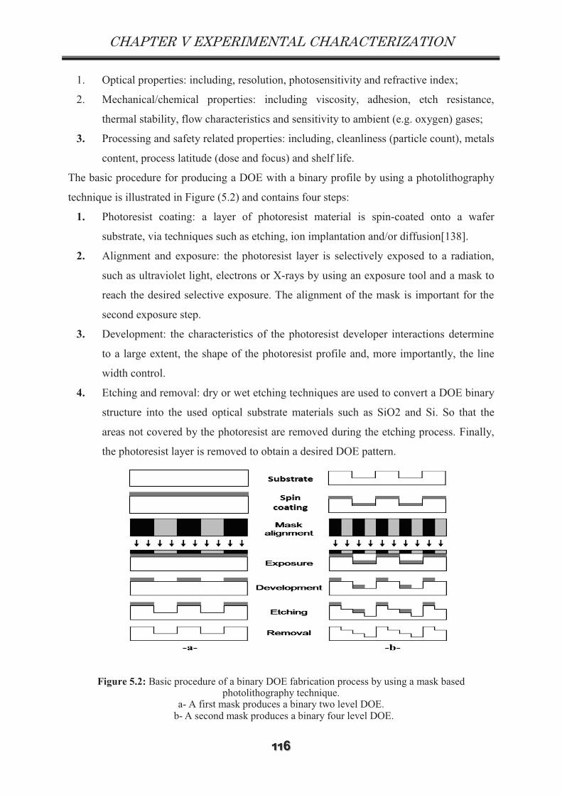
CHAPTER V EXPERIMENTAL CHARACTERIZATION
���
1. Optical properties: including, resolution, photosensitivity and refractive index;
2. Mechanical/chemical properties: including viscosity, adhesion, etch resistance,
thermal stability, flow characteristics and sensitivity to ambient (e.g. oxygen) gases;
3. Processing and safety related properties: including, cleanliness (particle count), metals
content, process latitude (dose and focus) and shelf life.
The basic procedure for producing a DOE with a binary profile by using a photolithography
technique is illustrated in Figure (5.2) and contains four steps:
1. Photoresist coating: a layer of photoresist material is spin-coated onto a wafer
substrate, via techniques such as etching, ion implantation and/or diffusion[138].
2. Alignment and exposure: the photoresist layer is selectively exposed to a radiation,
such as ultraviolet light, electrons or X-rays by using an exposure tool and a mask to
reach the desired selective exposure. The alignment of the mask is important for the
second exposure step.
3. Development: the characteristics of the photoresist developer interactions determine
to a large extent, the shape of the photoresist profile and, more importantly, the line
width control.
4. Etching and removal: dry or wet etching techniques are used to convert a DOE binary
structure into the used optical substrate materials such as SiO2 and Si. So that the
areas not covered by the photoresist are removed during the etching process. Finally,
the photoresist layer is removed to obtain a desired DOE pattern.
Figure 5.2: Basic procedure of a binary DOE fabrication process by using a mask based photolithography technique.
a- A first mask produces a binary two level DOE. b- A second mask produces a binary four level DOE.

CHAPTER V EXPERIMENTAL CHARACTERIZATION
��
The principles of photolithography provide the basis for the fabrication of binary diffractive
optical elements. In general, a DOE fabrication process using the photolithography technique
requires the achieving of five tasks[69]:
1. Generation of the DOE phase profile (via analytical or numerical techniques).
2. Generation of a standard format of mask layout compatible with the lithography
machine, such as GDSII, Oasis or Dxf from the DOE phase profile.
3. Generation of a photomask pattern by using laser or e-beam patterning system.
4. Generation of the master DOE element by using the photolithography techniques.
5. Generation of the mass production of DOE element by using a replication technique
such as embossing or injection molding.
Nowadays, some processes of mass production of DOE’s are based on a master fabrication
by using a conventional photolithography technique[72, 138]. However, there are several
disadvantages which are related to the production costs, the performance of the DOE and the
minimum feature size that can be manufactured. Furthermore, this technique requires many
process steps to fabricate binary multilevel DOE. It is expensive and time-consuming.
Furthermore, in the fabrication process of multilevel binary DOE’s master elements, it
should be noted that even small residual alignment errors between consecutive masking steps
can cause significant efficiency losses[140, 141]. The influence of mask alignment error
becomes unavoidable with very small feature sizes (i.e. etching steps size) around 1 µm in
actual DOE processes using a photolithography technique[142].
II. The "software" mask techniques
Alternative lithography techniques are based on the “software mask techniques” that have
been elaborated to overcome some limitations and problems related to the physical mask
techniques. The Direct write lithography uses a narrow beam of charged particles or photons,
and a “software” mask instead of a physical mask. These techniques include electron-beam
(e-beam) lithography[143], focused–ion beam[144] and laser lithography[145].These
techniques operate with a variation of the intensity of a beam based on a software mask, so
that the local exposure is proportional to the required depth of the resist. The disadvantages of
these direct writing processes is that they are inappropriate for a volume manufacturing
because of the serial nature of the processes, also the non-conventional sides walls effect that
caused by the finite writing spot size[1]. Grayscale lithography proposed after the software

CHAPTER V EXPERIMENTAL CHARACTERIZATION
��!
mask technique that is commonly used for the fabrication of the surface relief structures of
binary DOE’s. Gray scale lithography is usually implemented by using gray-tone masks,
which allow modulation of the intensity of light passing through the mask. Therefore,
grayscale fabrication methods offer the possibility to drastically reduce the number of
processing steps involved in generating a multilevel and monolithic DOE. In other hand,
these techniques provide the advantage of allowing the fabrication of multilevel DOE’s with
a single lithographic masking and one etching step for a large area at once, which allows a
high fabrication quantity. Grayscale lithography techniques also provide the possibility to
fabricate DOE’s with a high diffraction efficiency, in comparison with the conventional
physical mask lithography technique, as illustrated in Figure (5.3)[69].
Figure 5.3: Binary, multilevel, and analog surface-relief lithography fabrication process (Fresnel lens)[69].
Recently, new photolithographic techniques have been proposed to fabricate DOE’s. These
techniques are based on real-time reconfigurable masks, through using either a liquid crystal
display LCD or a digital or tilting micro-mirror device used as a spatial light modulator
(SLM) to control the light exposure [146, 147]. This technique was selected to fabricate our
proposed DOE’s, through cooperation with Telecom Bretagne (TB), through the use of a
parallel direct writing lithography device[149], which is available in TB.

CHAPTER V EXPERIMENTAL CHARACTERIZATION
��"
5.3 Parallel direct laser writing
The parallel direct laser writing grayscale lithography represents a very flexible technique
for the fabrication of DOE prototypes because it requires only a short fabrication time and is
more economical. The parallel write technique can be used to produce DOE’s with the
minimum feature size of a few micrometers, with a resolution that is better than 1 µm, and a
writing speed of around 20 mega pixels per second[148]. In principle, the main processes for
DOE fabrication by using parallel direct laser writing methods are the same as those used in
all other lithography techniques. Firstly, the proper photoresist layer is spin coated on a
substrate which is usually glass. The photoresist available in the Telecom Bretagne facility is
a positive photoresist (type S1800 series from Micro Resist Technology). This photoresist is
used to fabricate the master component of a DOE. This photoresist series has different
viscosities, which allows preparing different layers thicknesses ranging from a few hundreds
of nm to above 10 µm. The spin coating unit has a tolerance of about 20 nm for the
uniformity error of the photoresist layer in the coating process. Secondly, the DOE structure
relief profile is implemented on the photoresist layer by changing the light intensity
exposition using a programmable mask. The photoplotter wavelength that we used is 436 nm.
The basic principle of the parallel direct write photoplotter setup is shown schematically in
the Figure (5.4). A programmable Spatial Light Modulator (SLM) is used as a reconfigurable
mask, instead of a conventional fixed mask. The Liquid Crystal Display (LCD) currently
used in the photoplotter is a 1050 1400 pixels liquid crystal spatial light modulator (SLM).
A light source having a wavelength of 436 nm is used to illuminate the SLM, the light
intensity is adjusted for each pixel. As a result, the DOE pattern displayed on the SLM is
imaged on the substrate by the projection lens. The LCD is a monochromatic device with
gray-level bitmap images coded on 8 bits, theoretically producing gray levels ranging up to
256[149]. The photoplotter has the ability to align over one million modulated parallel
beams, corresponding to the SLM pixels. Therefore, an area up to a 6 4 mm2 (1.5 Mpixels)
can be exposed at the same time. A bigger area can be exposed in a short time about (1
cm2/min) by adjusting a 2D translation stage. Thirdly, the samples after the exposure process
are subject to the development step by putting them into the developer solution.
Consequently, the DOE desired pattern is etched into the photoresist layer. Finally, the DOE
structure relief profile can be etched into the substrate to obtain the master element for the
mass production, if it is necessary according to the applications needs. In our case, we used
the DOE produced after the development step, to verify the performance of the theoretical

CHAPTER V EXPERIMENTAL CHARACTERIZATION
�#$
model. The photographs of the spin-coating unit and the parallel direct write lithography unit
that exist in the clean room of Telecom Bretagne and that were used to fabricate the proposed
DOE are displayed in Figure (5.5).
Figure 5.4: The basic setup of the parallel direct writing lithography bench.
-a-
-b-
Figure 5.5: The lithography instruments that were used in the DOE fabrication processes in TB. a- Spin-coater unit b- Parallel direct-writing unit

CHAPTER V EXPERIMENTAL CHARACTERIZATION
�#�
5.4 Manufacturing process and characterization of DOE proposed
A grayscale lithography technique has been used to fabricate the multi-level microstructures
of the proposed DOE. A film of a positive photoresist type S1800 series was first coated onto
a clean glass substrate, with an appropriate spinning rate to be sure to obtain a uniform
thickness. The sample was then soft-baked on hotplate at 120 ºC for 5 min. The photoresist was
exposed using the parallel direct-write photoplotter, where the exposure dose is modulated
through the changing of the exposure time by using a mechanical shutter to ensure the optimum
etching depth. Consequently, the targeted DOE pattern is exposed by the grayscale process
concerning each pixel according to a calibration (via a programmable Spatial Light Modulator).
The photoresist was developed by Microposit 303A Developer to etch the exposed pattern,
followed by deionized DI water rinsing to obtain the final DOE profile. Some prototypes DOE’s
samples were fabricated in the cleanroom of Telecom Bretagne (TB), in the frame of a
collaborative program with the optics department of Telecom Bretagne. The purpose of the
fabrication is to demonstrate experimentally the performance of the targeted DOE. The fabricated
DOEs prototypes are for two different elements: first, a G-Fresnel device was designed by
merging a Diffractive Lens (DL) profile into a Diffraction Grating (DG) profile, which has the
following parameters; design wavelength 600 nm, focal length 15 cm, grating period 18 µm and
1µm pixel size. A G-Fresnel element was quantized into 8-level surface –relief structure and
fabricated on area of 1 cm x 1cm. Second, an off-axis diffractive lens was designed with the
following parameters; design wavelength 600 nm, focal length 15 cm, 1 µm pixel size, and
8-level quantized surface-relief structure on an area of 1 cm x 1 cm. The etching depth intended is
820 nm for the highest level (i.e. 8-level). The DOE’s were fabricated with three different
exposure times high, middle, and low which are arranged on the glass substrate as shown in
Figure (5.6).
Figure 5.6: Scheme that illustrates the arrangement and the exposure time for the DOEs fabricated.

CHAPTER V EXPERIMENTAL CHARACTERIZATION
�##
5.4.1 Structure profile characterization
Optical measurements were made for the photoresist profiles of the DOE's fabricated with a
micro profilometer. These measurements were performed using two types of instruments:
1. The Zygo NewView 7200 white light interferometer (profilometer) is a powerful tool
for characterizing and quantifying surface roughness, step heights, critical dimensions
and other micro topographical features with excellent precision and accuracy.
2. Atomic force microscopy (AFM), or scanning force microscopy (SFM), is a very
high-resolution type of scanning probe microscopy (SPM), with a demonstrated
resolution of some fractions of a nanometer that is more than 1000 times better than
the optical diffraction limit.
Figure (5.7) shows the images of these two instruments.
-a- -b-
Figure 5.7: Instruments used for the profilometer measurements of the fabricated DOE’s: a- Zygo NewView 7200 Optical Profiler.
b- Atomic Force Microscope and its working principle.
The profilometer measurements were used to characterize the micro feature side wall
sharpness and the etching depth in the photoresist profile of the DOE’s. These measurements
can determine the accuracy of the fabricated DOE's patterns, which must be of high quality
with the highest resolution possible, without defects or inhomogeneities in the global surface
flatness. Generally, the optical efficiency of a DOE is reduced when the actual height varies
from the designed height, because the profile errors produced by the fabrication process. The
first measurements performed using a Zygo profilometer, allow identifying the etching
profile of the fabricated DOE's. Figure (5.8) shows 3D interferometric micro images of an 8-
level etching profile for some fabricated DOE's.
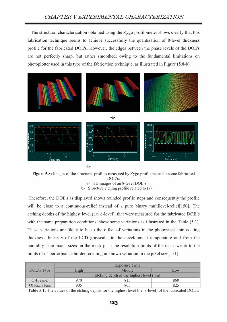
CHAPTER V EXPERIMENTAL CHARACTERIZATION
�#%
The structural characterization obtained using the Zygo profilometer shows clearly that this
fabrication technique seems to achieve successfully the quantization of 8-level thickness
profile for the fabricated DOE's. However, the edges between the phase levels of the DOE's
are not perfectly sharp, but rather smoothed, owing to the fundamental limitations on
photoplotter used in this type of the fabrication technique, as illustrated in Figure (5.8-b).
-a-
-b-
Figure 5.8: Images of the structures profiles measured by Zygo profilemeter for some fabricated DOE’s:
a- 3D images of an 8-level DOE’s. b- Structure etching profile related to (a).
Therefore, the DOE's as displayed shows rounded profile steps and consequently the profile
will be close to a continuous-relief instead of a pure binary multilevel-relief[150]. The
etching depths of the highest level (i.e. 8-level), that were measured for the fabricated DOE’s
with the same preparation conditions, show some variations as illustrated in the Table (5.1).
These variations are likely to be to the effect of variations in the photoresist spin coating
thickness, linearity of the LCD grayscale, in the development temperature and from the
humidity. The pixels sizes on the mask push the resolution limits of the mask writer to the
limits of its performance border, creating unknown variation in the pixel size[151].
DOE’s Type Exposure Time
High Middle Low Etching depth of the highest level (nm)
G-Fresnel 970 815 860 Off-axis lens 905 805 825
Table 5.1: The values of the etching depths for the highest level (i.e. 8-level) of the fabricated DOE's.

CHAPTER V EXPERIMENTAL CHARACTERIZATION
�#&
Second measurements were done by using an Atomic Force Microscope (AFM) to identify
accurately the actual etching profile and the surface topography for selected fabricated DOE.
This measurement was performed for an Off-axis diffractive lens that was fabricated with a
middle exposure time. AFM measurements were performed over a square area of 25 µm x 25
µm and for different selected positions of the DOE surface, as shown in Figure (5.9). It is
clear that the structure is close to a continuous profile and also that the surface roughness for
each level is not flat.
Figure 5.9: AFM image of the DOE tested.
There is a variation in the etching depth of the highest level and for every level from one
position to another one in the profile, as shown in Figure (5.10). The depth values of the
highest level are around 810 nm in one location and 841 nm in another location, and they are
around 153 nm and 133 nm in two different locations for one level, as shown in Figure (5-10-
a and b) respectively. This is due to the sensitivity of the grayscale profile to the developing-
time and to the resist thickness, that could lead to a few tens of nm deviation of the etching
depth profile for one place to another[152].
-a-
-b- Figure 5.10: The etching depth for different locations of the profile for the DOE selected:
a- The etching depth for the highest level (i.e. 8-level). b- The etching depth for only one level.

CHAPTER V EXPERIMENTAL CHARACTERIZATION
�#'
Therefore, it is expected that these variations in the etching depth, will have an impact on the
optical performance of a DOE. This issue will be discussed in the next paragraph.
5.4.2 Optical characterization
The first attempt to conduct the optical performance characterization for the fabricated
DOE has been implemented through using two monochromatic light sources, which are
helium neon laser (λ=633 nm) and low noise laser (λ=473 nm). The beam analyzer with
Beamstar FX software was used to verify from the optical efficiency performance of the
fabricated DOE prototypes. The output of these two sources was magnified using a Leitz PL
40/0.65 Microscope Objective Lens 160 mm to overcome the combination of the desired
diameter output beam and the CCD pixel size of 4.8 μm (H) by 3.6 μm (V). The collimated
beam of light was guided through diaphragm to illuminate the whole DOE surface at normal
incidence. Whereas, the area of DOE surface is bigger than the area of CCD camera surface.
Therefore, the convex lens that has a focal length of 20 cm was used to concentrate the full
beam on the surface of the CCD camera. The strategy that used to calculate experimentally
the diffraction efficiency is based on measuring two values by using the CCD camera of the
beam analyzer. First, we calculate the light power intensity over the area of laser beam (Pb)
that equivalent to the area of DOE surface. Second, we calculate the light power intensity that
concentrated by a DOE in the focal point (Pf) and at the first diffraction order. Finally, the
diffraction efficiency ( will be calculated as a ratio of the Pf to the Pb as explained in the
following equation:
(5.1)
The example of an optical measurement using the beam analyzer for the fabricated
prototype of an off-axis lens is shown in Figure (5.11).
-a- -b- Figure 5.11: Optical measurements of the light power intensity using the beam analyzer.
a- Light power intensity over the area of laser beam. b- Light power intensity at the focal point and at the first diffraction order.

CHAPTER V EXPERIMENTAL CHARACTERIZATION
�#�
Matlab code was used to calculate the light power intensity values of both the Pf and the
Pb. The diffraction efficiency (DE) values that have calculate from both theoretically using
numerical simulation and experimentally for the fabricated DOE using two laser sources as
explained in Table (5.2):
Wavelength (nm) DE-Theoretically DE-Experimentally
633 86.51 82.85 473 57.10 39.02
Table 5.2: Comparison between theoretical and experimental values for a diffraction efficiency of an off-axis lens for two wavelengths.
These preliminary results show that there is a good agreement between a theoretical and
experimental measurements at least for the He Ne laser source that is very close to design
wavelength of this DOE.
The goal is to verify experimentally the performance of the proposed DOE model for large
spectrum band (i.e. the intended spectrum for this application). Therefore, the optical
performance characterization was performed for the fabricated DOE by using a particular
optical setup, as shown in Figure (5.12). A Tungsten Halogen lamp from Ocean Optics (type
HL-2000) was used as a white light source which supplies the Vis-NIR of the spectrum
range. This source is coupled to an optical fiber. Two convex lenses that have two different
focal lengths (f1=10 cm and f2=20 cm) were used to obtain a collimated white-light beam. A
diaphragm has been placed to obtain a beam with a diameter equivalent the surface size of the
DOE. In this manner, a collimated beam of light was guided to illuminate the DOE surface at
normal incidence. A multi-mode fiber tip detector with a diameter of 600 µm was placed on
the transmission side at the DOE image plane at distance of d =11.25 cm. The fiber tip was set
on a translation stage with a movement precision of , it was scanned across the entire
surface distance of both of the two bands of the targeted spectrum. The finite diameter of the fiber
tip and the stage accuracy will undoubtedly limit the resolution of the spectral-spatial image-map
measurement. The other end of the fiber was connected to an Ocean Optics Maya pro
Spectrometer, where the spectrum information can be extracted and analysed by a computer with
the oceanview software. A polarizer was placed between the two lenses to reduce the excess of
light power which can lead to an error in the calculation due to the saturation of the
spectrometer CCD detector.

CHAPTER V EXPERIMENTAL CHARACTERIZATION
�#
-a- -b-
Figure 5.12: The optical setup for the fabricated DOE characterization. a- Schematic diagram of the optical setup.
b- Image of the optical setup.
A G-Fresnel and an Off-axis diffractive lens were optically characterized by measuring the
spectral characteristics of their diffraction patterns at a distance d=11.25 cm, that represents
the expected place of the spectrum splitting. The spectrum splitting can be clearly observed
by placing a white plate right at this distance, as shown in Figure (5.13). The important thing
that must be clarified about this Figure, it related to the colors of the second separated band
(i.e. 800-1100 nm). We can see that the colors of this band are in the range of the visible
spectrum, while in fact they consist of the wavelengths in the range of the near infrared
spectrum. This because, the total light power intensity distribution for the wavelengths of
band1, won't just focused in the first diffraction order, which means not all light power of
band1 will be arrived to the surface of PV1 cell. But in fact, the light power intensity of band1
will be focused in several diffraction orders for some wavelengths, which leads to some part
of the light power will be arrived to the surface of PV2 cell. For this reason, we see the colors
related to the visible spectrum in the expected position of band2.
Figure 5.13: Photograph at the separation distance that prove clearly the effect of the spectrum splitting of the fabricated DOE.

CHAPTER V EXPERIMENTAL CHARACTERIZATION
�#!
The performance of both devices (G-Fresnel and an Off-axis lens) have been obtained by
measuring the spectrum as a function of the position in the reconstruction plane considered as
a spatial–spectral map. Where each row in this map corresponds to the spatial distribution of
the diffracted light power at their respective wavelength. Figure (5.14) shows the spatial-
spectral maps for the G-Fresnel device and for the Off-axis diffractive lens that were
fabricated with different exposure times (i.e. High Exposure Time (HET), Middle Exposure
Time (MET), and Low Exposure Time (LET)). It is clear from the Figure (5.14), that the
spatial distribution of the diffracted light power for the fabricated DOE's is compatible with
the intended model.
The transmission or optical efficiency (i.e. diffraction efficiency) was calculated for the
fabricated DOE's, for each band separated with the proposed theoretical model. Therefore
firstly, the total input power was calculated over the entire DOE area for each wavelength.
The adopted methodology to calculate these values is based on the working principle of the
spectrometer through using the ocean view software for analysis the spectrum. The
spectrometer can be used to implement several optical measurements of spectrum analysis.
We calculated the transmission value of the intended spectrum by measuring the light
intensity represented by the account of CCD spectrometer camera. After that, the Matlab
code has been used to calculate the spatial distribution of light power of each wavelength of
the intended spectrum over the entire DOE area. Second, the total power is calculated for
each wavelength at the expected separation distance and over all the area for each band
separated from the spectrum. The same aforementioned methodology has been again used to
implement this measurement. Finally, the optical efficiency for each wavelength of the
separated band is calculated as the ratio between the values of the second step to the first step,
and as explained in the following equations:
(5.2)
(5.3)
Where and are the optical efficiencies at each wavelength of band1 and band2
respectively. Whereas, all the wavelengths of band1 will be absorbed by PV1 cell and all the
wavelengths of band2 will be absorbed by a PV2 cell. N, N1, and N2 are the integer numbers
of a translation stage with movement precision of 100 µm over the DOE area, band1 area and
band2 respectively.

CHAPTER V EXPERIMENTAL CHARACTERIZATION
�#"
-a- -b-
Figure 5.14: Map of the spatial spectral distribution of the diffracted light power at respective wavelength of the fabricated DOE’s.
a- Map produced from G-Fresnel devices fabricated with different exposure times. b- Map produced from an Off-axis diffractive lens fabricated with different exposure
times. The measurements of the optical efficiencies are shown in Figure (5.15) for the fabricated
DOE’s with three exposure times. In the case of a G-Fresnel device: Firstly, for the element
fabricated with the HET, the optical efficiency values are higher for the wavelengths of the
band2, in comparison to the values of the wavelengths of the band1, as shown in Figure(5.15-
a). Secondly, for the element fabricated with the MET, the optical efficiency values are

CHAPTER V EXPERIMENTAL CHARACTERIZATION
�%$
increased for the wavelengths of the band1 at the expense of the values of the wavelengths of
the band2 that are decreased. In this fabrication condition, the optical efficiency average
values of the wavelengths from both bands are higher than 50%, as shown in Table (5.3).
Thirdly, for the element fabricated with the LET, the optical efficiency values continue to
increase for the wavelengths of the band1 at the expense of the values of the wavelengths of
the band 2, that are continue to decrease. This behavior is due to the results of a combination
of errors introduced during fabrication in the pixel heights and errors in the dispersion of the
photoresist[153]. The optical performance characterization is in good agreement with the
structure profile characterization. Whereas, the best optical performance was obtained for a
G-Fresnel device fabricated at the MET, because the depth profile is very close to the desired
one as explained in Table (5.1).
In the case of an off-axis lens device. The comparison is performed between the values of
the optical diffraction efficiencies obtained experimentally and the values obtained from the
simulations, as shown in Figures (5.15-b). The general performance of the fabricated off-axis
diffractive lens shows a good agreement with the design of the proposed model, but with
some variations in the values obtained due to errors of fabrication as aforementioned. An off-
axis diffractive lens as fabricated shows generally a better performance compared to the
fabricated G-Fresnel as already explained in chapter 4, regardless of the fabrication
conditions. The best optical performance was obtained for an Off-axis lens device fabricated
at the LET, because the depth profile is very close to the desired one as explained in Table
(5.1). In this case, the optical efficiency average values of the wavelengths for the both bands
are about 60 %. However, this result does not closely match with the simulation results. The
optical efficiency average value that was measured for the wavelengths of the band1 is
smaller compared to the value obtained from the simulation. While, the optical efficiency
average value that was measured for the wavelengths of the band2 is higher compared to the
value obtained from the simulation, as shown in Table (5.4).

CHAPTER V EXPERIMENTAL CHARACTERIZATION
�%�
-a- -b-
Figure 5.15: The optical diffraction efficiency as a function of the wavelength for the fabricatedDOE’s. The solid line with the marks by circles and squares represent the real measurements, while,
the marks by circles and squares alone represent the results of the simulation. a- Experimental results for the fabricated G-Fresnel devices.
b- Comparison between the simulation and the measured results for the fabricated Off-axis lenses.

CHAPTER V EXPERIMENTAL CHARACTERIZATION
�%#
This difference can be attributed to several reasons related to fabrication errors and to the
optical setup used in the measurements. In addition, this measurement was implemented
without taking into account the reflection effect, which expected with antireflection coating
this difference will be reduced. From a fabrication viewpoint, these DOE’s have been
prepared as prototypes without very precise fabrication constraints. As we explained in the
paragraph 5.4.1 the structure depth profiles are characterized by the non-homogeneous
thicknesses over all the surfaces of the DOE's fabricated. These errors will lead to a change of
the phase shift of the wavefront for a given wavelength, which means that the light power
density will be distributed in many diffraction orders. In addition, from the measurements
viewpoint, the light source which was used in the experimental optical setup is not very
accurately collimated. Furthermore, the optical power density is not also accurately uniform
for all the wavefront.
Exposure Time Band1 400-800 nm
PV1 cell
Band2800-1100 nm PV2 cell
( ( ( ( High 42.20 32.67 69.60 7.11
Middle 52.07 27.04 61.34 12.42 Low 55.88 17.44 46.12 15.81
Table 5.3: Optical efficiency average values of wavelengths for the separated bands and for a G-Fresnel device fabricated with the different exposure times. The ( and ( represent the lighting power of all the wavelengths for each separated band, that focus on the desired and undesired
PV cell respectively.
Exposure
Time
Measured Simulated
Band1 400-800 nm
PV1 cell
Band2 800-1100 nm
PV2 cell
Band1 400-800 nm
PV1 cell
Band2 800-1100 nm
PV2 cell
( ( ( ( ( ( ( (
High 46.58 30.02 68.18 8.33 71.40
14.19
52.27
10.09
Middle 52.57 22.95 60.37 10.92
Low 58.56 22.88 58.02 13.97 Table 5.4: Optical efficiency average values of the wavelengths for the separated bands and for an
Off-axis diffractive lens device fabricated with the different exposure times, and the values obtained from the simulation for the same device.

CHAPTER V EXPERIMENTAL CHARACTERIZATION
�%%
5.5 Conclusion
In conclusion, the more efficient selection of the DOE's fabrication technique that will be
used to prepare the master element for the mass production, it will depend on the type, the
size of their feature sizes, and the material. In the case of the fabrication of DOE’s with a
multilevel profile, the parallel direct laser writing grayscale lithography is one of the
preferable techniques that we have identified. This maskless photolithography technique is
characterized by a short fabrication time, which makes it cheaper. Furthermore, this
technique can be used to implement DOE’s with a small feature size (about a few
micrometers), and with a resolution that is better than one micrometer. The main observed
characteristic of this technique is the producing of rounded profile steps, which induces to
make the DOE profile structure to be a continuous-relief instead of a binary multilevel-relief.
Furthermore, one can notice that this technique permits a limited control on the uniformity of
the depth profile or the inhomogeneity of the etch depth across whole DOE’s surface. The
structure feature profile characterization of the prototypes DOEs that we have fabricated
shows clearly the aforementioned positive and negative properties of this technique. The
AFM measurements show clearly the rounding effect in the structure depth profile of the
DOE's fabricated. The optical characterizations illustrate the credibility of the proposed
DOE's design related to the performance of the prototypes DOE's that we have fabricated.
The large spectrum splitting and the beam concentration have been confirmed experimentally
by the DOE’s proposed and fabricated. In general, the optical efficiency performance is
always similar for both the theoretical and the experimental measurements, and for the full
spectrum range of the two separated bands. Some variations appeared between the
experimental and the theoretical measurements of the optical performance, they can be
attributed to errors in both the fabrication and the optical measurement. In addition, these
measurements were made without taking in account the reflection effect. Thereby, we expect
that a very close matching between the theoretical and the experimental measurements can be
obtained from the elements manufactured by this easy and cheap lithography technology,
after overcome these manufacturing restrictions. Furthermore, the optical characterizations
are measured with a more precise optical setup, after integrating an Anti-Reflection (AR)
coating with the fabricated DOE.

GENERAL CONCLUSION AND PRESPECTIVES
���
General Conclusion and Perspectives
Sunlight is one of the important candidates for renewable and environmentally friendly
energy sources. Sunlight can provide a large part of the energy required in the world during
the year, due to the plenitude of sunny days over the year and long hours of the sun beams
that arrive into a large part of the earth's surface. Photovoltaic (PV) cells are devices that are
used to convert the sunlight energy into electrical power. The third generation PV cells (i.e.
the multijunction or tandem PV cells) have the highest conversion efficiency among all PV
cell types. Lateral multijunction PV cells represent the most efficient technique, with
satisfying fabrication simplicity and with quite low costs. This PV cell type requires an
optical device that can implement spectrum splitting and beam concentration (SSBC)
simultaneously. Diffractive optical elements (DOE’s) seem most suited for this application.
This is thanks to many functions that these elements can implement, such as the accurate and
smart control of light distribution, and the possibility to build high quality compact solar cell
system out of DOE.
The main goal of this thesis was to design and to experimentally validate diffractive optical
element that can meet the optical functions (i.e. SSBC) required for the specific type of the
PV cells mentioned above. In order to reach this aim, all the diffractive optical theories that
can be used in the design and the performance modelling of the DOE's were studied.
Consequently, rigorous modelling tools were developed, that are based on these diffraction
theories. These tools have been used for two purposes: Firstly, for the modelling and the
design of a particular DOE’s structure profile, which is from a subwavelength type. Secondly,
an hybrid propagator method (FDTD-ASM) has been proposed to simulate rigorously the
electromagnetic field propagation in subwavelength DOE’s structure profile and that can
operate in the far field.
Two validating diffractive optical elements have been designed to implement the SSBC.
Their performances were tested in simulation by using the proposed rigorous hybrid
propagator (FDTD-ASM). These two elements are: a G-Fresnel (grating + Fresnel diffractive
lens) device, and an off-axis diffractive lens device. These DOE devices are coded with a
multilevel and a subwavelength structure profile. The simulated and experimental
performance of these devices showed their ability to split the solar spectrum in the visible and
near infrared range (i.e. 400-1100 nm), into two bands 400-800 nm, and 800-1100 nm with a
low concentration factor. The simulation results showed the ability to achieve about 70%

GENERAL CONCLUSION AND PRESPECTIVES
��
optical diffraction efficiency in both the bands separated, for the devices proposed and
designed with optimal parameters. An off-axis diffractive lens achieves better performance
compared to a G-Fresnel, and this performance is in theory better with a subwavelength
structure compared to a multilevel quantized profile. An experimental validation was
performed for the designed devices, through the manufacturing of a prototype with 8-level
structure profile, by using specific and available fabrication technique. Grayscale lithography
technique is a preferred technology for the fabrication multilevel DOE's that has structure of
a small feature size in the range of a few micrometers. The structure profile characterization
clarified the restrictions of this technology that are related to the limits in the sharpness of the
structure edges and the uniformity of the general DOE structure profile. The optical
characterization results were set experimentally and confirm that the fabricated DOE's fit
roughly the simulation results of the DOE’s proposed and designed. The variation that
appears between the experimental and the simulation results are attributed to the fabrication
errors in the prototypes structure depth profile. Consequently, we expect that a better
matching can be obtained between the experimental and the simulation results of the DOE
proposed, if DOE's are fabricated by using a higher accuracy manufacturing technique.
This thesis present promising results in terms of efficiency, for compact DOE device, that
can be used to achieve spectral splitting and beam concentration simultaneously for
applications in the lateral multjunction PV cells. In the course of the PhD thesis project
concerning this topic, numerous ideas were formulated that can be used as starting point for
further research in the future. DOE's with a more rigorous subwavelength structure can allow
a high control of the distribution for the light propagation. We expect that DOE's can achieve
a spectrum splitting for many bands with a high concentration factor. Furthermore, the
metasurface technology of the subwavelength structure represents a promising research topic.
Metasurface structures have demonstrated the ability to implement the functions that we
studied (i.e. SSBC) with a higher accuracy performance [21, 154].

APPENDIX A
��!
Thin Element Approximation
The thin element approximation (TEA) is the approach used to describe the propagation of a
light field through diffractive optical elements that have a thickness comparable with the
wavelength used. This approximation assumes that no diffraction occurs inside the structure
of a DOE. The illuminating wave passes the DOE without changing in the propagation
direction. The optical field just past the DOE can be described by a complex transmission
function:
(A.1)
The is the Fresnel transmission coefficient and is given by:
(A.2)
Where n1 and n2 are the refractive indices of the incident and the exiting media respectively,
θ1 and θ2 are the angle of the incident and the angle of refraction with respect to the optical
axis.
T(x,y) is the amplitude modulation (0 of an amplitude DOE which has a
square aperture. Therefore, this transmission function can take two values:
(A.3)
The light propagates without absorption in phase elements, i.e. T(x, y) =1. The wavefronts
are modified by the phase shift θ(x, y) passing through the DOE depth profile. The DOE
depth profile is quantized into an N-level phase profile and illuminated by a plane wave at a
normal incidence in free space, as shown in Figure (A.1). Therefore, the optical path
difference (OPD) between two rays transmitted through any quantized level step of a
thickness can be calculated as[69]:
(A.4)
The phase shift of any quantized level will be:
(A.5)
The phase of the plane wave is periodic with the period of 2 . Therefore, the phase shift step
should be .
The depth of each multilevel phase profile can be found from the relation [69, 126]:

APPENDIX A
��"
(A.6)
Scalar wave equation (Helmholtz equation)
The derivation of the Helmholtz equation from Maxwell's equations will be explained in this
appendix. The scalar approximations are developed by recasting Maxwell’s equations into a
scalar form, where all components of the electric and the magnetic field can be summarized
by a single scalar wave equation. As the propagation medium is homogeneous (ϵ=0) in the
free space region. It is possible to reduce Maxwell's equations into a single scalar wave
equation. Taking the curl of both sides of both Ampere's law and Faraday's law, and by using
the identity which holds for any vector A:
(A.7)
The Helmoltz equation can be derived in the same way and is defined as follows:
(A.8)
The refractive index is defined according to the relation , where is the relative
permittivity, such that , with the permittivity of empty space. Whereas, the light
speed in vacuum is defined by the relation . In the same way, the wave
equation for the magnetic field can be derived:
(A.9)
Thus, both fields satisfy the same equation, and each spatial component of the field vectors
also satisfies the same equation. Therefore, the vector equation (A.8) and (A.9) can be
reduced to the scalar equation (with representing a spatial component of the field vector):
Uo d
Ф=2
U d
n2 nn1
Figure A.1: A diffractive optic interface that shows the propagation of the light through an N-level phase DOE based on the TEA.

APPENDIX A
��#
(A.10)
We assume a monochromatic wave expressed by:
(A.11)
Where denotes taking real component. Here we also use the definition:
(A.12)
Inserting Eq (A.9) into Eq (A.10) yields the Helmoltz equation:
(A.13)
From this equation, scalar solutions to various diffraction problems can be derived.

APPENDIX B
��$
Scalar Diffraction Theory limitations
Scalar diffraction theory treats the interaction between the incident optical field and the DOE
as a retardation in the optical path on the incident field. Therefore, a phase delay will be
added to the incident field, because of the change in the optical path length through the field
in the DOE profile, as shown in Figure (B.1)
Figure B.1: Scalar (thin-phase) approximation for the interaction between an incident field and a diffractive structure[1].
The optical diffraction field can be represented by scalar diffraction theory as the scalar thin
element approximation (TEA), as explained in appendix A. This theory will fail to predict,
all the components of the electromagnetic fields. Therefore, the diffractive field (diffraction
pattern) after the DOE structure will consist of only the two components, i.e. ,
for TE polarization, with a phase shift due to the Optical Path Length Difference (OPLD).
We can see clearly from Figure (B.2), that the scalar diffraction theory and the rigorous
diffraction theory don’t produce same behavior of interaction for the electromagnetic field
with different structure profile of DOE. Therefore, the value of the phase and the amplitude
will not be the same after the DOE structure (binary element structure). These values are
calculated using the TEA in scalar diffraction theory, and, they have also been calculated by
the FDTD method in the rigorous diffraction theory. The diffracted field obtained by the
FDTD simulation is a complex instead of a real function as predicted by the TEA. As a result,
the far field diffraction pattern will not have Hermitian symmetry as it is predicted by the
scalar diffraction theory[69, 73].
Furthermore, the scalar diffraction theory will be not useful to predict the electromagnetic
coupling effect for all the field components along the boundary of the DOE profile, and it

APPENDIX B
��%
introduces errors in the analysis. This case appears especially when the DOE has dimensions
that are equal, or less than, to the wavelength of illumination. The non-uniformities of the
electromagnetic field in the boundary becomes very clear with the decreasing of the features
size of the DOE, as illustrated in Figure (B.3) from the top to bottom.
Figure B.2: Normalized amplitude of Ey for TE polarization (a) and phase (b) of the diffracted field
which have been calculated immediately after the binary element DOE by using the TEA, in
comparison with the FDTD simulation (MEEP)[92].
Non- uniformities in the electric field, along the DOE boundary are produced because of the
increased influence of electromagnetic coupling effects over the boundary. Therefore, a more
rigorous analysis method must be used to predict the interaction behavior of the
electromagnetic field with the DOE.
Figure B.3: Individual plots of the electric field amplitude along the boundary of a DOE, for
different periods. The wavelength for each case was 1µm. The vertical axis that represents local
values of the electric field amplitude are in volt per meter[1].

APPENDIX B
���
The scalar diffraction theory based on the TEA is commonly used for the design and the
analysis of diffractive optical elements (DOEs). The approach is valid as long as the DOE
feature size is large compared to the wavelength used, and the element thickness is
comparable to the light wavelength. However, the validity breaks down in the cases where
the period-length to wavelength ratio decreases, or when the element is too thick. Therefore,
in many DOE structures, the influence of the shadowing will be very remarkable and cannot
be predicted by the TEA in the scalar diffraction theory[155]. Generally, two types of
shadowing effect are found in the DOE structure; Shadow between two neighboring periods
and Shadow between two neighboring ‘‘stairs’’ (phase levels), as shown in Figure (B.4).
Figure B.4: Shadowing Effects produced in a DOE structure.
D. Pommet [156] found that the scalar diffraction theory will be valid with an error ( >5%),
when the minimum feature size is less than 14 wavelength (s<14λ). This error is minimized
when the fill factor approaches 50%, even for small feature size(s=2λ). While, S. Millen[99]
found that the scalar diffraction theory is a viable method for the design of DOE's, provided
that their minimum feature size is not less than the illumination wavelength.

APPENDIX C
��&
Numerical stability and dispersion
Traditionally, the numerical implementation of FDTD requires to ensure a numerical stability
of the algorithm for a linear model, which is achieved through the fulfilling of the Courant
factor. The stability conditions are based on the spatial lattice resolution and temporal step
adopted for propagation of the electromagnetic wave among spatial lattice location.
Therefore, the size of the space lattice increments must selected to be small enough to cover
the fine details of the distribution of ε and the electromagnetic field components in the
structures. Thus, for instance:
(C.1)
Where is the highest refractive index in the simulation domain[89]. As well, the time
step of the wave propagation is related to the size of the spatial increment:
(C.2)
Where c is light speed in a propagation medium. These constraints are necessary to avoid the
effects of numerical instability[157]. In case of execution the FDTD algorithm. This
numerical instability, often, causes the total energy within the FDTD computational grid to
diverge toward infinity, which is physically unreliable. In order to ensure that the FDTD
algorithm converges to the correct result, the temporal resolution step must be small enough
to precisely describe the propagation of the light between two nearest neighbors:
(C.3)
Where S is the Courant factor which is satisfied: S , is the number of dimensions
in the simulation.
The numerical implementation of FDTD also causes some degree of dispersion of the
simulated wave modes in the computational lattice, which is referred to as a numerical
dispersion. The phase velocity of the wave modes in the FDTD grid differs from the true
speed of light in the medium in which it propagates. In the FDTD, the speed of light can in
fact, vary with the modal wavelength, the direction of propagation in the grid and with the
size of the Yee grid cells[89]. The FDTD grid in essence behaves like a “numerical
aether”[158]. Such that an electromagnetic wave interacts within the structure and will
generally propagate with a slower velocity. Consequently the wave propagation will
accumulate phase errors, which can possibly lead to a waveform broadening, a spurious

APPENDIX C
���
anisotropy and a pseudo refraction. Generally the effect of the numerical dispersion should be
accounted in the procedure of the FDTD implementation. Especially, in case of large
electrical structures by using dispersion-optimized Yee algorithms. In principle, if the
computational lattice is discretized with more Yee cells (of smaller size), the effects of
numerical dispersion become less significant
Boundary conditions
To mode the wave propagation phenomena in a domain which extends to infinity, it is a
common practice to truncate the computational domain into a finite domain. The FDTD
method solves electromagnetic problems in a finite calculation lattice. Thus, the fields are
known only at discrete points. Maxwell's equations are approximated by using finite-
differences which generate one equation for every field component at every point. These
equations include field components at surrounding points. At the edge of the grid, it will be
required to include a field component that is outside of the grid which really doesn't exist. On
the other hand, to obtain physically reasonable solutions in scattering problems, the
calculation lattice must be truncated at the lattice edges via proper boundary conditions that
extend the lattice to infinity, creating an illusion of an unbounded volume. Accurate boundary
treatment is of course not only important for the accuracy along the edge, but it is of great
concern for the entire computation since the errors generated near the boundary propagate
into the domain. Generally, three well known types of the boundary conditions have been
used for implementing the FDTD algorithm numerically:
1. Absorbing Boundary conditions (ABC)
Homogeneous Dirichlet boundary conditions [77] for the wave equation lead to a total reflection
of an impinging wave on the artificial boundary of a computational domain. ABC is a
reflectionless absorbing layer (i.e. Prefect metallic well), that surrounds the lattice and absorbs all
incident waves, regardless of the angle of incidence and wave length. This condition just
assumes that the fields outside the grid are all zeros.
2. Periodic Boundary conditions (PBC)
The periodic boundary condition is used in the FDTD modeling for periodic electromagnetic
devices, such as diffraction gratings and metamaterials. The electromagnetic fields inside a
periodic structure takes the same symmetry and periodicity of that structure according to the
Bloch theorem. For a device that is a periodic structure with period ʌ, the electromagnetic
field components are periodic also U( )=U( +ʌ), where is the vector direction in all the
three directions ). Therefore, the periodic boundary condition can be written in a

APPENDIX C
���
more general form, which is named Floquet-Bloch boundary. The periodic values of the field
components in any direction can be calculated as; , where is the wave
factor. In numerical simulation, they assume that the fields outside the “left side” of the grid
are exactly the same as the fields at the far “right side” of the grid. Thus, it is possible to use
the fields on the right side of the grid in place of the fields outside the left side of the grid,
and also around.
3. Prefect Match Layer (PML)
The Perfectly Matched Layer is defined as: an absorbing boundary Layer, which is a layer of
artificial absorbing material that essentially acts as a loosy Material. The PML was originally
proposed by J. P. Berenger in 1994[159], for solving the problem of absorbing boundaries for
wave equation. The PML is placed adjacent to the edges of the computational grid which is
completely independent of the boundary condition. The PML absorbs all incident waves,
regardless of the angle of incidence and wavelength, and prevents their reflection. Beranger’s
original formulation is called the split-field PML, because the field components in PML
regions are split into two unphysical field components to obtain additional degrees of freedom.
Nowadays, a more common formulation is the uniaxal PML or UPML, which expresses the PML
region as the ordinary wave equation, with a combination of artificial anisotropic absorbing
materials[160]. This modification allows to create a reflectionless interface among the
computational cell and the PML layer. In the numerical implementation, the PML in the actual
discretized system has some small reflection which makes it imperfect [161, 162]. The finite
thickness of a PML layer causes some reflection of the incident EM waves, which bounce back to
the main lattice via a reflection from the prefect electric conductor layer terminating the
calculation domain. Therefore, the PML implementation requires the conductivity to be
smoothly increased from zero to a maximum value, over a distance of a few grid points.

REFERENCES
��
[1] D. C. O'Shea, T. J. Suleski, A. D. Kathman et al., [Diffractive optics, Design, Fabriction, and
Test], SPIE,The international Society for Optical Enginerring(2004).
[2] H. Hoppe, and N. S. Sariciftci, “Organic solar cells: An overview”, Journal of Materials
Research, 19(7), 1924-1945 (2004).
[3] M. A. Green, “Third generation photovoltaics: Ultra-high conversion efficiency at low
cost”, Progress in Photovoltaics, 9(2), 123-135 (2001).
[4] W. Shockley, and H. J. Queisser, “Detailed Balance Limit of Efficiency of p-n Junction Solar
Cells”, J. Appl. Phys(32), 510 (1961).
[5] C. L. Tan, and Y. T. Lee, “High-efficiency light-trapping effect using silver nanoparticles on
thin amorphous silicon subwavelength structure”, Optics Letters, 38(23), 4943-4945
(2013).
[6] E. E. Perl, C. T. Lin, W. E. McMahon et al., “Ultrabroadband and Wide-Angle Hybrid
Antireflection Coatings With Nanostructures”, Ieee Journal of Photovoltaics, 4(3), 962-967
(2014).
[7] K. Li, H. Sun, F. Ren et al., “Tailoring the Optical Characteristics of Microsized InP
Nanoneedles Directly Grown on Silicon”, Nano Letters, 14(1), 183-190 (2014).
[8] S. W. Baek, G. Park, J. Noh et al., “Au@Ag Core-Shell Nanocubes for Efficient Plasmonic
Light Scattering Effect in Low Bandgap Organic Solar Cells”, Acs Nano, 8(4), 3302-3312
(2014).
[9] C. I. Yeo, Y. M. Song, S. J. Jang et al., “Optimal design of nano-scale surface light trapping
structures for enhancing light absorption in thin film photovoltaics”, Journal of Applied
Physics, 114(2), (2013).
[10] H. Helmers, A. W. Bett, J. Parisi et al., “Modeling of concentrating photovoltaic and
thermal systems”, Progress in Photovoltaics, 22(4), 427-439 (2014).
[11] Q. Huang, J. Wang, B. Quan et al., “Design and fabrication of a diffractive optical element
as a spectrum-splitting solar concentrator for lateral multijunction solar cells”, Applied
Optics, 52(11), 2312-2319 (2013).
[12] C. Konstantopoulos, and E. Koutroulis, “Global Maximum Power Point Tracking of Flexible
Photovoltaic Modules”, Ieee Transactions on Power Electronics, 29(6), 2817-2828 (2014).
[13] C. H. Chang, J. A. Dominguez-Gaballero, H. J. Choi et al., “Nanostructured gradient-index
antireflection diffractive optics”, Optics Letters, 36(12), 2354-2356 (2011).
[14] M. Wellenzohn, and R. Hainberger, “Light trapping by backside diffraction gratings in
silicon solar cells revisited”, Optics Express, 20(1), A20-A27 (2012).
[15] R. Rothemund, T. Umundum, G. Meinhardt et al., “Light trapping in pyramidally textured
crystalline silicon solar cells using back-side diffractive gratings”, Progress in Photovoltaics,
21(4), 747-753 (2013).
[16] I. Mingareev, R. Berlich, T. J. Eichelkraut et al., “Diffractive optical elements utilized for
efficiency enhancement of photovoltaic modules”, Optics Express, 19(12), 11397-11404
(2011).
[17] R. M. Swanson, [Handbook of Photovoltaic Science and Engineering, chapter11,
Photovoltaic Concentrators], John Wiley & Sons, Ltd, 449-503 (2005).
[18] P. Benitez, R. Mohedano, M. Buljan et al., "Ultra-High Efficiency, High-Concentration PV
System Based On Spectral Division Between GaInP/GaInAs/Ge And BPC Silicon Cells", AIP
Conference Proceedings. 1407(2011).
[19] G. Kim, J. A. Dominguez-Caballero, H. Lee et al., “Increased Photovoltaic Power Output via
Diffractive Spectrum Separation”, Physical Review Letters, 110(12), 123901 (2013).
[20] M. Gordon, D. Zhang, S. Vorndran et al., "Planar Holographic Spectrum-Splitting PV
Module Design", Proceedings of SPIE. 8468(2012).
[21] Y. Yao, H. Liu, and W. Wu, “Spectrum splitting using multi-layer dielectric meta-surfaces
for efficient solar energy harvesting”, Applied Physics a-Materials Science & Processing,
115(3), 713-719 (2014).

REFERENCES
���
[22] A. S. Lin, [Modeling of Solar Cell Efficiency Improvement Using Optical Gratings and
Intermediate Absorption Band], PhD thesis, University of Michigan, (2010).
[23] [http://www.ise.fraunhofer.de/en/press-and-media/press-releases/presseinformationen-
2013/world-record-solar-cell-with-44.7-efficiency].
[24] Martin A. Green, Keith Emery, Yoshihiro Hishikawa et al., “Solar Cell Efficiency
Tables(Version 32),” Prog. Photovolt: Res. Appl, 16, 435–440 (2008).
[25] [http://phys.org/news/2014-12-nrel-efficiency-solar-cell.html].
[26] A. G. Imenes, and. D. R. Mills, “Spectral beam splitting technology for increased conversion
efficiency in solar concentrating systems: a review”, Solar Energy Materials and Solar Cells
84,(Issues 1–4), 19–69 (2004).
[27] R. M. Swanson, “The promise of concentrators,” Progress in Photovoltaics, 8(1), 93-111
(2000).
[28] G. L. A. Antonio Luque, [Solar cells and optics for photovoltaic concentration], A. Hilger,
Bristol, England ; Philadelphia,(1989).
[29] R. leutz, and A. Suzuki, [Nonimaging Fresnel Lenses: design and performance of solar
concentrators], Springer, Verlag Berlin Heidelberg(2001).
[30] J. C. Minano, P. Benitez, P. Zamora et al., “Free-form optics for Fresnel-lens-based
photovoltaic concentrators”, Optics Express, 21(9), A494-A502 (2013).
[31] M. Buljan, J. C. Minano, P. Benitez et al., “Improving performances of Fresnel CPV systems:
Fresnel- RXI Kohler concentrator”, Optics Express, 22(5), A205-A210 (2014).
[32] P. Benitez, J. C. Minano, P. Zamora et al., “High performance Fresnel-based photovoltaic
concentrator,” Optics Express, 18(9), A25-A40 (2010).
[33] J. H. Karp, E. J. Tremblay, and J. E. Ford, “Planar micro-optic solar concentrator”, Optics
Express, 18(2), 1122-1133 (2010).
[34] T. Waritanant, S. Boonruang, and T. Y. Chung, “High angular tolerance thin profile solar
concentrators designed using a wedge prism and diffraction grating”, Solar Energy, 87, 35-
41 (2013).
[35] R. K. Kostuk, J. Castro, B. Myer et al., [Holographic Elements in Solar Concentrator and
Collection Systems], SPIE, (2009).
[36] D. Chemisana, M. Victoria Collados, M. Quintanilla et al., “Holographic lenses for building
integrated concentrating photovoltaics”, Applied Energy, 110, 227-235 (2013).
[37] B. Pesala, “Planar Solar Concentrators using Subwavelength Gratings”, Frontiers in Optics
2011/Laser Science XXVII, paper FWZ3, (2011).
[38] O. D. Miller, E. Yablonovitch, and S. R. Kurtz, “Strong Internal and External Luminescence
as Solar Cells Approach the Shockley-Queisser Limit”, Ieee Journal of Photovoltaics, 2(3),
303-311 (2012).
[39] J. ED, [Areas for improvement of the semiconductor solar energy converter: In transaction
of the conference on the use of solar energy], University of Arizona press, Tuscan.
Arizona(1955).
[40] Moon. R. L., James. L. w., Vander. P. H. A. et al., "Multigap solar cell requirements and the
performance of AlGaAs and Si cells in concentrated sunlight", In: Photovoltaic Specialists
Conference, 13th, Washington D. C.(1978).
[41] F. Dimroth, and S. Kurtz, “High-efficiency multijunction solar cells”, Mrs Bulletin, 32(3),
230-235 (2007).
[42] R. R. King, D. C. Law, K. M. Edmondson et al., “40% efficient metamorphic
GaInP/GaInAs/Ge multijunction solar cells”, Applied Physics Letters, 90(18), (2007).
[43] L. M. Fraas, J. E. Avery, J. Martin et al., “Over 35-percent efficient GaAs/GaSb tandem solar
cells”, Ieee Transactions on Electron Devices, 37(2), 443-449 (1990).
[44] R. R. King, D. Bhusari, D. Larrabee et al., “Solar cell generations over 40% efficiency,”
Progress in Photovoltaics, 20(6), 801-815 (2012).

REFERENCES
��
[45] A. Polman, and H. A. Atwater, “Photonic design principles for ultrahigh-efficiency
photovoltaics”, Nature Materials, 11(3), 174-177 (2012).
[46] B. Mitchell, G. Peharz, G. Siefer et al., “Four-junction spectral beam-splitting photovoltaic
receiver with high optical efficiency”, Progress in Photovoltaics, 19(1), 61-72 (2011).
[47] A. Barnett, D. Kirkpatrick, C. Honsberg et al., “Very High Efficiency Solar Cell Modules”,
Progress in Photovoltaics, 17(1), 75-83 (2009).
[48] A. Mojiri, R. Taylor, E. Thomsen et al., “Spectral beam splitting for efficient conversion of
solar energy-A review”, Renewable & Sustainable Energy Reviews, 28, 654-663 (2013).
[49] D. E. Osborn, M. A. C. Chendo, M. A. Hamdy et al., “Spectral selectivity applied to hybrid
concentration systems”, Solar Energy Materials, 14(3-5), 299-325 (1986).
[50] M. A. C. Chendo, M. R. Jacobson, and D. E. Osborn, “Liquid and thin-film filters for hybrid
solar energy conversion systems ” Solar & Wind Technology, 4(1), 131-138 (1987).
[51] J. C. C. Fan, and F. J. Bachner, “Transparent heat mirrors for solar energy applications”,
Applied Optics, 15(4), 1012-1017 (1976).
[52] D E. Soule, and S E. Wood, "Heat-Mirror Spectral Profile Optimization for TSC Hybrid Solar
Conversion", Proc. SPIE, V. 72, 172-180 (1986).
[53] S. R. Clark, [Spectrovoltaic solar energy conversion system], Patent, Us 4350837 (1982).
[54] U. Ortabasi, “A Hardened solar concentrator system for space power-generation-
PhotoVoltaic Cavity converter(PVCC)”, Space Technology-Industrial and Commercial
Applications, 13(5), 513-523 (1993).
[55] W. H. Bloss, M. Griesinger, and E. R. Reinhardt, “Dispersive concentrating systemsbased on
transmission phase holograms for solar applications”, Applied Optics, 21(20), 3739-3742
(1982).
[56] J. E. Ludman, J. Riccobono, I. V. Semenova et al., "The optimization ofa holographic system
for solar power generation", Solar Energy, 60(1), 1-9 (1997).
[57] A. Goetzberger, and W. Greubel, “Solar-energy conversion with fluorescent collectors”,
Applied Physics, 14(2), 123-139 (1977).
[58] F. Galluzzi, and E. Scafe, “Spectrum shifting of sunlight by luminescent sheets-
performance evaluation of photovoltaic applications”, Solar Energy, 33(6), 501-507 (1984).
[59] M. Sabry, R. Gottschalg, T. R. Betts et al., “Optical filtering of solar radiation to increase
performance of concentrator systems”, Conference Record of the Twenty-Ninth Ieee
Photovoltaic Specialists Conference 2002, 1588-1591 (2002).
[60] Y. Zhao, M.-Y. Sheng, W.-X. Zhou et al., “A solar photovoltaic system with ideal efficiency
close to the theoretical limit”, Optics Express, 20(1), A28-A38 (2012).
[61] D. Lin, E. Torrey, J. Leger et al., “Lossless holographic spectrum splitter in lateral
photovoltaic devices”, Photovoltaic Specialists Conference (PVSC), 37th, IEEE, 978(1),
(2011).
[62] A. Goetzberger, J. C. Goldschmidt, M. Peters et al., “Light trapping, a new approach to
spectrum splitting”, Solar Energy Materials and Solar Cells, 92(12), 1570-1578 (2008).
[63] M. Stefancich, A. Zayan, M. Chiesa et al., “Single element spectral splitting solar
concentrator for multiple cells CPV system”, Optics Express, Vol. 20, Issue 8, pp. 9004-
9018, 20(8), 9004 (2012).
[64] D. Vincenzi, A. Busato, M. Stefancich et al., “Concentrating PV system based on spectral
separation of solar radiation”, Physica Status Solidi a-Applications and Materials Science,
206(2), 375-378 (2009).
[65] C. M. Horwitz, “A new solar selective surface,” Optics Comm., 11, 210-212 (1974).
[66] J. M. Castro, D. Zhang, B. Myer et al., “Energy collection efficiency of holographic planar
solar concentrators”, Applied Optics, 49(5), 858-870 (2010).
[67] C. Michel, J. Loicq, F. Languy et al., “Optical study of a solar concentrator for space
applications based on a diffractive/refractive optical combination”, Solar Energy Materials
& Solar Cells, 120(part A), 183–190 (2014).

REFERENCES
��!
[68] Y. Jia-Sheng, W. Jin-Ze, H. Qing-Li et al., “A single diffractive optical element implementing
spectrum-splitting and beam-concentration functions simultaneously with high diffraction
efficiency”, Chinese Physics B, 22(3), 34201 (2013).
[69] B. C. Kress, and P. Meyrueis, [Applied Digital Optics: From Micro-optics to Nanophotonics],
John Wiley & Sons, Ltd, (2009).
[70] D. W. Sweeney, and G. E. Sommargren, “Harmonic diffractive lenses”, Applied Optics,
34(14), 2469-2475 (1995).
[71] G. J. Swanson, [Binary optics technology: the theory anddesign of multi-level phase
diffractive optical elements], MIT, Cambridge, Mass.(1989).
[72] J. W. Goodman, [Introduction to Fourier Optics] Roberts & company Publisher (2005).
[73] I. Richter, P. C. Sun, F. Xu et al., “Design considerations of form birefringent
microstructures”, Applied Optics, 34(14), 2421-2429 (1995).
[74] S. D. Mellin, [Design and Analysis of finite aperature diffractive optical elements], PhD
thesis, University of Alabama, Huntsville(2001).
[75] O. K.Ersoy, [Diffaction, Fourier Optics and Imaging] A John Wiley & Sons, Inc, Hoboken,
New jersy(2007).
[76] M. Born., and E. Wolf, [Principles of Optics], Cambridge University Press,(1999).
[77] Y. Y. Feng Di, Jin Guofan, Tan Qiaofeng, and Haitao, Liu, “Rigorous electromagnetic design
of finite-aperture diffractive optical elements by use of an iterative optimization
algorithm”, J. Opt. Soc. Am. A, 20(9), 1739-1746 (2003).
[78] J. W. Goodman, [Introduction to Fourier Optics] McGrow Hill, San Fransico(1968).
[79] R. Martinez-Herrero, P. M. Mejias, S. Bosch et al., “Vectorial structure of nonparaxial
electromagnetic beams”, Journal of the Optical Society of America a-Optics Image Science
and Vision, 18(7), 1678-1680 (2001).
[80] Y. Q. Zhao, and Y. P. Li, “Vector iterative algorithms for beam shaping”, Optical
Engineering, 42(11), 3080-3081 (2003).
[81] P. Liu, and B. Lu, “The vectorial angular-spectrum representation and Rayleigh-
Sommerfeld diffraction formula”, Optics and Laser Technology, 39(4), 741-744 (2007).
[82] M. S. Mirotznik, D. W. Prather, and J. N. Mait, “A hybrid finite element boundary element
method for the analysis of diffractive elements”, Journal of Modern Optics, 43(7), 1309-
1321 (1996).
[83] D. W. Parther, M. S. Mirotznik, and J. N. Mait, “Boundary integral methods applied to the
analysis of diffractive optical elements”, J. Opt. Soc. Am. A, 14(1), 34--43 (1997).
[84] D. W. Parther, M. S. Mirotznik, and J. N. Mait, “Boundary element method for vector
modeling diffractive optical elements”, Proc. SPIE, 2404, 28-39 (1995).
[85] B. Lichtenberg, and N. C. Gallagher, “Numerical modeling of diffractive devices using the
finite -element method”, Optical Engineering, 33(11), 3518-3526 (1994).
[86] E. P. Michel Neviere, [Light Propagation in Periodic Media: Differential Theory and Design]
Marcel Dekker, Inc, (2002).
[87] M. G. Moharam, and T. K. Gaylord, “Rigorous coupled-wave analysis of planar-grating
diffraction,” J. Opt. Soc. Am., 71(7), 811--818 (1981).
[88] L. F. Li, “Formulation and comparison of two recursive matrix algorithms for modeling
layered diffraction gratings”, J. Opt. Soc. Am. A, 13(5), 1024-1035 (1996).
[89] A. Taflove, and S. C. Hagness, [Computational Electrodynamics: The Finite-Difference Time-
Domain Method, Third Edition] Artech House, (2005).
[90] Y. Kane, “Numerical solution of initial boundary value problems involving maxwell's
equations in isotropic media”, Antennas and Propagation, IEEE Transactions on, 14(3), 302-
307 (1966).
[91] W. F. Ames, [Numerical Methods for Partial Differential Equations] Acedemic Press, New
York,(1997).

REFERENCES
��"
[92] G. N. Nguyen, [Modeling,Design and Fabrication of Diffractive Optical Elements based on
nanostructures operating beyond the scalar paraxial domain], PhD thesis, Universite de
Bretagne, Télécom Bretagne, Brest, France(2014).
[93] M. Born, and E. Wolf, [Principle of Optics] Pregamon press, London(1964).
[94] H. Kikuta, Y. Ohira, H. Kubo et al., “Effective medium theory of two-dimensional
subwavelength gratings in the non-quasi-static limit”, J. Opt. Soc. Am. A, 15(6), 1577-1585
(1998).
[95] P. Lalanne, and D. LemercierLalanne, “On the effective medium theory of subwavelength
periodic structures”, Journal of Modern Optics, 43(10), 2063-2085 (1996).
[96] J. Jiang, [Rigorous Analysis and design of diffractive optical elements], PhD thesis,
University of Alabama in Huntsville(2000).
[97] F. Wyrowski, “Diffractive optical elments: iterative calculation of quantized, blazed phase
structures”, Journal of the Optical Society of America a-Optics Image Science and Vision,
7(6), 961-969 (1990).
[98] F. Wyrowski, and O. Bryngdahl, “Iterative Fourier transform algorithem applied to
computer holography”, Journal of the Optical Society of America a-Optics Image Science
and Vision, 5(7), 1058-1065 (1988).
[99] S. D. Mellin, and G. P. Nordin, “Limits of scalar diffraction theory and an iterative angular
spectrum algorithm for finite aperture diffractive optical element design”, Optics Express,
8(13), 705-722 (2001).
[100] S. Y. a. M. Yamamoto, [Design and evaluation of diffractive optical elements: optimization
by using iterative angular spectrum approach and evaluation based on vector diffraction
theory] ,SPIE, (2009).
[101] Brain K. Jennison, Jan P. Allebach, and Donald W. Sweeney “Efficient design of direct-
binary-search computer-generated holograms”, J. Opt. Soc. Am. A, 8(4), 652--660 (1991).
[102] M. A. Seldowitz, J. P. Allebach, and D. W. Sweeney, “Synthesis of digital holograms by
binary search”, Applied Optics, 26(14), 2788-2798 (1987).
[103] M. S. Kim, and C. C. Guest, “Simulated annealing algorithem for binary phase only filters in
pattern-classification”, Applied Optics, 29(8), 1203-1208 (1990).
[104] A. G. Kirk, and T. J. Hall, “Design of binary computer generated holograms by simulated
annealing- coding density and reconstruction error”, Optics Communications, 94(6), 491-
496 (1992).
[105] E. G. Johnson, and M. A. G. Abushagur, “Microgenetic-algorithem optimization methods
applied to dielectric gratings”, Journal of the Optical Society of America a-Optics Image
Science and Vision, 12(5), 1152-1160 (1995).
[106] T. Shirakawa, K. L. Ishikawa, S. Suzuki et al., “Design of binary diffractive microlenses with
subwavelength structures using the genetic algorithm”, Optics Express, 18(8), 8383-8391
(2010).
[107] Physical chemistry laboratory School of chemistry., [www.tau.ac.il/~phchlab/experiments-
new/semB01Hydrogen02/TheoreticalBackground.html].
[108] E. G. Loewen, M. Neviere, and D. Maystre, “Grating efficiency theory as it applies to blazed
and holographic gratings”, Applied Optics, 16(10), 2711-2721 (1977).
[109] J. Michael. Miller, Mohammed R. Taghizadeh, Jari Turunen, and Neil Ross, “Multilevel-
grating array generators: fabrication error analysis and experiments”, Appl. Opt., 32(14),
2519--2525 (1993).
[110] [http://users.telenet.be/cool_things_with_fresnel_lenses/what_are_fresnel_lenses.htm].
[111] Dale A. Buralli, G. Michael Morris, and John R. Rogers, “Optical performance of
holographic kinoforms”, Appl. Opt., 28(5), 976--983 (1989).
[112] D. Faklis, and G. M. Morris, “Spectral properties of multiorder diffractive lenses”, Applied
Optics, 34(14), 2462-2468 (1995).

REFERENCES
�#$
[113] [Massachusetts Institute of Technology, MEEP (MIT Electromagnetic Equation
Propagation), Website: ab-initio.mit.edu/wiki/index.php/Meep], (2014).
[114] W. F. Michael, “Binary gratings with increased efficiency”, Appl. Opt., 31(22), 4453--4458
(1992).
[115] E. Noponen, J. Turunen, and F. Wyrowski, “Synthesis of paraxial- domain diffractive
elements by rigorous electromagnetic theory”, Journal of the Optical Society of America a-
Optics Image Science and Vision, 12(5), 1128-1133 (1995).
[116] S. Astilean, P. Lalanne, P. Chavel et al., “High-efficiency subwavelength diffractive element
patterned in a high-refractive-index material for 633 nm”, Optics Letters, 23(7), 552-554
(1998).
[117] P. Lalanne, S. Astilean, P. Chavel et al., “Blazed binary subwavelength gratings with
efficiencies larger than those of conventional echelette gratings”, Optics Letters, 23(14),
1081-1083 (1998).
[118] D. W. Prather, J. N. Mait, M. S. Mirotznik et al., “Vector-based synthesis of finite aperiodic
subwavelength diffractive optical elements”, Journal of the Optical Society of America a-
Optics Image Science and Vision, 15(6), 1599-1607 (1998).
[119] Joseph N. Mait, Dennis W. Prather, and Mark S. Mirotznik, “Binary subwavelength
diffractive-lens design”, Opt. Lett., 23(17), 1343--1345 (1998).
[120] D. Feng, Y. B. Yan, and Q. F. Tan, "Vector-based synthesis of finite aperiodic diffractive
micro-optical elements with subwavelength structures' as beam deflectors", Proceedings
of the Society of Photo-Optical Instrumentation Engineers (Spie). 5253, 429-432 (2003).
[121] T. Oonishi, T. Konishi, and K. Itoh, “Deterministic design of binary phase-only blazed
grating with subwavelength features under limitation on spatial resolution of fabrication
technique,” Applied Optics, 46(22), 5019-5026 (2007).
[122] V. Raulot, P. Gerard, B. Serio et al., “Comparison of the behavior of a subwavelength
diffractive lens in TE and TM polarization allowing some nonstandard functions”, Optics
Letters, 36(7), 1194-1196 (2011).
[123] J. Yang, Z. Zhou, H. Jia et al., “High-performance and compact binary blazed grating
coupler based on an asymmetric subgrating structure and vertical coupling”, Optics
Letters, 36(14), 2614-2616 (2011).
[124] J. Yang, Z. Zhou, W. Zhou et al., “High Efficient Subwavelength Binary Blazed Grating Beam
Splitter via Vertical Coupling”, Ieee Photonics Technology Letters, 23(13), 896-898 (2011).
[125] G.-G. Kang, Q. F. Tan, and G. F. Jin, “Optimal Design of an Achromatic Angle-Insensitive
Phase Retarder Used in MWIR Imaging Polarimetry”, Chinese Physics Letters, 26(7), (2009).
[126] P. Lalanne, and M. Hutley, “The optical properties of artificial media structured at a
subwavelength scale”, Encyclopedia of optical engineering, 62-71 (2003).
[127] H. Kikuta, H. Yoshida, and K. Iwata, “Ability and limitation of effective medium theory for
subwavelength gratings”, Optical Review, 2(2), 92-99 (1995).
[128] H. Haidner, D. Dias, L. L. Wang et al., “Binary subwavelength structures resonance gratings
as polarization elements”, Pure and Applied Optics, 7(6), 1347-1361 (1998).
[129] Y. Yu, and L. Cao, “The phase shift of light scattering at sub-wavelength dielectric
structures”, Optics Express, 21(5), 5957-5967 (2013).
[130] F. Languy, K. Fleury, C. Lenaerts et al., “Flat Fresnel doublets made of PMMA and PC:
combining low cost production and very high concentration ratio for CPV”, Optics Express,
19(10), A280-A294 (2011).
[131] C. Yang, K. Shi, P. Edwards et al., “Demonstration of a PDMS based hybrid grating and
Fresnel lens (G-Fresnel) device”, Optics Express, 18(23), 23529-23534 (2010).
[132] C. Yang, P. Edwards, K. Shi et al., “Proposal and demonstration of a spectrometer using a
diffractive optical element with dual dispersion and focusing functionality”, Optics Letters,
36(11), 2023-5 (2011).

REFERENCES
�#�
[133] F. Languy, and S. Habraken, “Performance comparison of four kinds of flat nonimaging
Fresnel lenses made of polycarbonates and polymethyl methacrylate for concentrated
photovoltaics”, Optics Letters, 36(14), 2743-2745 (2011).
[134] C. L. F. Languy, J. Loicq, and S. Habraken, Darmstadt, Germany,(Achromatization of solar
concentrator thanks to diffractive optics), 2nd International Workshop on Concentrating
Photovoltaic Optics and Power, (2009).
[135] C. L. F. Languy, J. Loicq, T. Thibert and S. Habraken,, "Achromatization of solar
concentrators with diffractive optics", poster for universite de liege, Lab Holo.
[136] A. Rammohan, P. K. Dwivedi, R. Martinez-Duarte et al., “One-step maskless grayscale
lithography for the fabrication of 3-dimensional structures in SU-8”, Sensors and Actuators
B-Chemical, 153(1), 125-134 (2011).
[137] C. Mack, [Fundamental Principles of Optical Lithography: The Science of Microfabrication]
John Wiley & Sons, Ltd, (2007).
[138] L. F. Thompson, O. G. Wilson, M. J. Bowden and H. Hennig, [Introduction to
microlithography, Theory, Materials, and Processing] , American Chemical Society, (1983).
[139] M. B. Stern, and S. S. Medeiros, “Deep three-dimensional mi-crostructure fabrication for
infrared binary optics”, J. Vac. Sci. Technol., B10, 2520 –2525 (1992).
[140] M. B. Stern, M. Holz, S. S. Medeiros, and R. E. Knowlden, “Fabricating binary optics:
process variables critical to opti-cal efficiency”, J. Vac. Sci. Technol. B, 9, 3117–3121 (1991).
[141] Y. Unno, “Point-spread function for binary diffractive lenses fabricated with misaligned
masks,” Applied Optics, 37(16), 3401-3407 (1998).
[142] U. Yasuyuki, “Fabrication of N-level binary optical elements by use of M mask patterns
with N in the range of 2m-1+ 1 ≤ N ≤ M2,Appl. Opt., 37(34), 8012--8020 (1998).
[143] A. Pepin, V. Studer, D. Decanini et al., “Exploring the high sensitivity of SU-8 resist for high
resolution electron beam patterning”, Microelectronic Engineering, 73-4, 233-237 (2004).
[144] M. D. Henry, M. J. Shearn, B. Chhim et al., “Ga+ beam lithography for nanoscale silicon
reactive ion etching”, Nanotechnology, 21(24), (2010).
[145] M. T. Gale, M. Rossi, J. Pedersen et al., “Fabrication of continuous relief micro-optical
elements by direct laser writing in photoresists”, Optical Engineering, 33(11), 3556-3566
(1994).
[146] Q. J. Peng, S. J. Liu, Y. K. Guo et al., “Real-time photolithographic technique for fabrication
of arbitrarily shaped microstructures”, Optical Engineering, 42(2), 477-481 (2003).
[147] Y. Q. Gao, T. Z. Shen, J. S. Chen et al., “Research on high-quality projecting reduction
lithography system based on digital mask technique,” Optik, 116(7), 303-310 (2005).
[148] C. Rensch, S. Hell, M. Vonschickfus et al., “Laser scanner for direct writing lithography”,
Applied Optics, 28(17), 3754-3758 (1989).
[149] M. V. Kessels, M. El Bouz, R. Pagan et al., “Versatile stepper based maskless
microlithography using a liquid crystal display for direct write of binary and multilevel
microstructures”, Journal of Micro-Nanolithography Mems and Moems, 6(3), (2007).
[150] T. Hessler, M. Rossi, R. E. Kunz et al., “Analysis and optimization of fabrication of
continuous-relief diffractive optical elements”, Applied Optics, 37(19), 4069-4079 (1998).
[151] L. Mosher, C. M. Waits, B. Morgan et al., “Double-Exposure Grayscale Photolithography,”
Journal of Microelectromechanical Systems, 18(2), 308-315 (2009).
[152] R. Murali, [Nanotechnology Open Textbook, Chapter 5.2 Supplement – Grayscale
Lithography] Georgia Institute of Technology, Microelectronics Research Center(2007).
[153] Peng Wang, Josh A. Dominguez-Caballero et. al, “A new class of multi-bandgap high-
efficiency photovoltaics enabled by broadband diffractive optics”, Progress in
Photovoltaics: Research and Applications, (2014).
[154] F. Aieta, M. A. Kats, P. Genevet et al., “Multiwavelength achromatic metasurfaces by
dispersive phase compensation”, Science, 347(6228), 1342-1345 (2015).

REFERENCES
�#%
[155] U. Levy, E. Marom, and D. Mendlovic, “Thin element approximation for the analysis of
blazed gratings: simplified model and validity limits”, Optics Communications, 229(1-6),
11-21 (2004).
[156] D. A. Pommet, M. G. Moharam, and E. B. Grann, “limits of scalar diffraction theory for
diffractive phase elements”, Journal of the Optical Society of America a-Optics Image
Science and Vision, 11(6), 1827-1834 (1994).
[157] A. Taflove, and M. E. Brodwin, “Numerical solution of steady-state electromagnetic
scattering problems using the time-dependent Maxwell's equations”, Microwave Theory
and Techniques, IEEE Transactions on, 23(8), 623-630 (1975).
[158] S. L. Ray, “Numerical dispersion and stability characteristics of time-domain methods on
nonorthogonal meshes”, Ieee Transactions on Antennas and Propagation, 41(2), 233-235
(1993).
[159] J. P. Berenger, “A perfectly matched layer for the absorption of electromagnetic waves”,
Journal of Computational Physics, 114(2), 185-200 (1994).
[160] Z. S. Sacks, D. M. Kingsland, R. Lee et al., “A perfectly matched anisotropic absorber for use
as an absorbing boundary condition”, Ieee Transactions on Antennas and Propagation,
43(12), 1460-1463 (1995).
[161] A. F. Oskooi, L. Zhang, Y. Avniel et al., “The failure of perfectly matched layers, and
towards their redemption by adiabatic absorbers”, Optics Express, 16(15), 11376-11392
(2008).
[162] P.-R. Loh, A. F. Oskooi, M. Ibanescu et al., “Fundamental relation between phase and
group velocity, and application to the failure of perfectly matched layers in backward-
wave structures”, Physical Review E, 79(6), (2009).