Embed Size (px)
Citation preview
5414 IEEE TRANSACTIONS ON POWER ELECTRONICS, VOL. 28, NO. 11, NOVEMBER 2013
Multiprobe Measurement Method forVoltage-Dependent Capacitances of Power
Semiconductor Devices in High VoltageKe Li, Arnaud Videt, Member, IEEE, and Nadir Idir, Member, IEEE
Abstract—The characterization of voltage-dependent capaci-tances of power semiconductor devices [diode, MOSFET, insulatedgate bipolar transistor (IGBT), etc.] is very important for model-ing their dynamic performances. A measurement method usingtwo current probes has been developed to characterize interelec-trode capacitances of power devices while isolating the measure-ment devices from the high-voltage dc bias power source. Cissand Coss are shown to be accurately measured while Crss is notconvincing enough. Then an additional current probe is added toimprove the method. Crss is shown to be well characterized by thisthree-current-probe method. This method has been validated us-ing various technologies of semiconductor devices including siliconMOSFET and silicon carbide JFET. The interelectrode capaci-tances of power devices can be safely and accurately measuredwith this multiprobe method even in high voltage.
Index Terms—Current probes, high voltage, power semicon-ductor devices, silicon carbide (SiC), silicon, voltage-dependentcapacitances.
I. INTRODUCTION
POWER devices are widely used in power electronic sys-tems to achieve highly efficient energy conversion [1]–[4].
Thus, it is necessary to know their characteristics for betteruse [5], [6]. Recently, with the emergence of the silicon carbide(SiC) and gallium nitride (GaN) power devices to realize a highpower density, high efficiency, and high temperature power con-verter [7]–[12], their modeling becomes important in the aimof a high-speed commutation system design [13], [14], electro-magnetic compatibility (EMC) aspect [15], etc. Power deviceshave interelectrode capacitances which are generally voltage de-pendent [16]. They not only play an important role on the powerdevice commutation (notably influencing switching losses andEMC behavior), but also are involved in the parasitic resonancesthat occur at the end of the turn-off commutation (thereby influ-encing the overall spectrum of electromagnetic noise level [17]).How to characterize these capacitances determines the accuracyof their models [18], [19].
Manuscript received October 29, 2012; revised December 14, 2012; acceptedJanuary 7, 2013. Date of current version May 3, 2013. Recommended for pub-lication by Associate Editor A. Lindemann.
The authors are with the Laboratory of Electrical Engineering and PowerElectronics (L2EP), University of Lille 1, Villeneuve d’Ascq 59650, France(e-mail: [email protected]; [email protected]; [email protected]).
Color versions of one or more of the figures in this paper are available onlineat http://ieeexplore.ieee.org.
Digital Object Identifier 10.1109/TPEL.2013.2240016
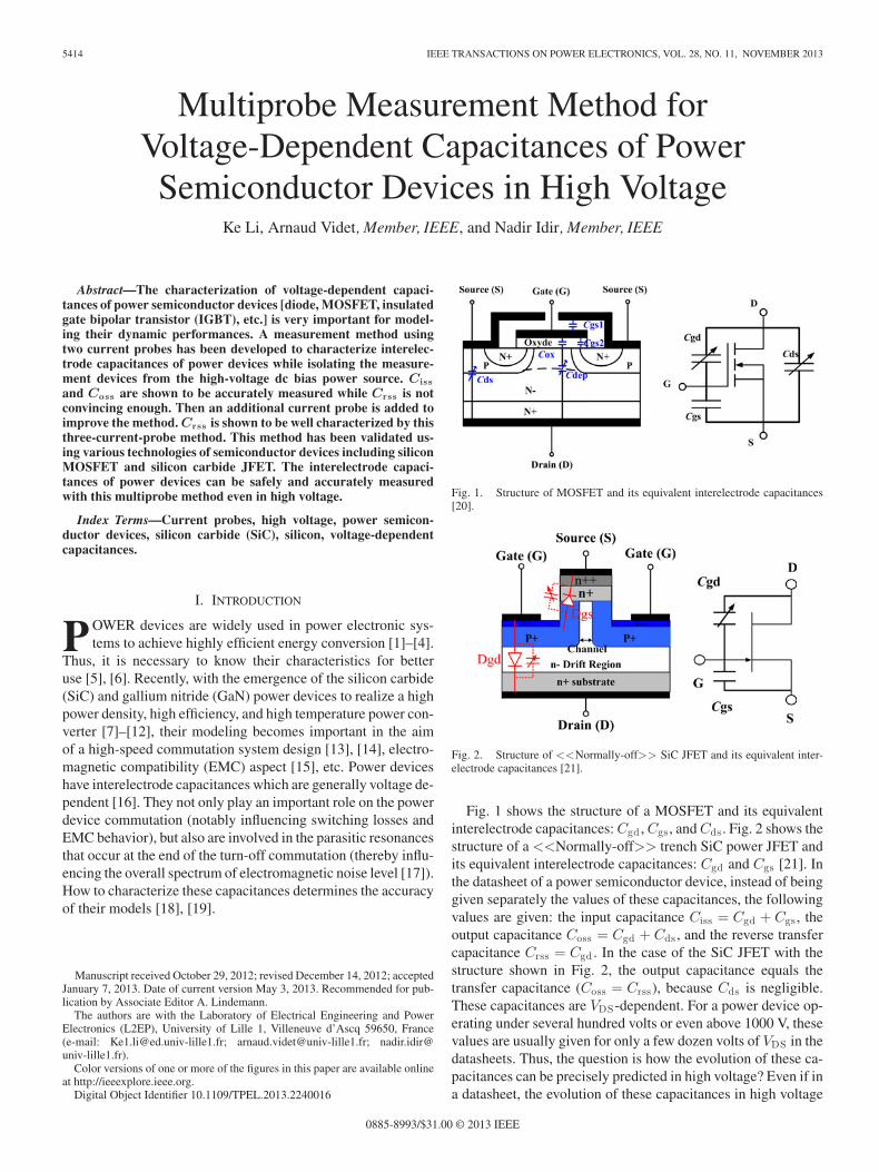
Fig. 1. Structure of MOSFET and its equivalent interelectrode capacitances[20].
Fig. 2. Structure of <<Normally-off>> SiC JFET and its equivalent inter-electrode capacitances [21].
Fig. 1 shows the structure of a MOSFET and its equivalentinterelectrode capacitances: Cgd , Cgs , and Cds . Fig. 2 shows thestructure of a <<Normally-off>> trench SiC power JFET andits equivalent interelectrode capacitances: Cgd and Cgs [21]. Inthe datasheet of a power semiconductor device, instead of beinggiven separately the values of these capacitances, the followingvalues are given: the input capacitance Ciss = Cgd + Cgs , theoutput capacitance Coss = Cgd + Cds , and the reverse transfercapacitance Crss = Cgd . In the case of the SiC JFET with thestructure shown in Fig. 2, the output capacitance equals thetransfer capacitance (Coss = Crss), because Cds is negligible.These capacitances are VDS -dependent. For a power device op-erating under several hundred volts or even above 1000 V, thesevalues are usually given for only a few dozen volts of VDS in thedatasheets. Thus, the question is how the evolution of these ca-pacitances can be precisely predicted in high voltage? Even if ina datasheet, the evolution of these capacitances in high voltage
0885-8993/$31.00 © 2013 IEEE
LI et al.: MULTIPROBE MEASUREMENT METHOD FOR VOLTAGE-DEPENDENT CAPACITANCES OF POWER SEMICONDUCTOR DEVICES 5415
happens to be provided by manufacturers, can these values bereliable? It is not rare that the characteristic of a power devicedoes not follow the exact information in a datasheet, especiallyfor SiC and GaN power devices whose datasheets are often pre-liminary and can be updated within a few months. It also needsto be noted that C–VDS curves in datasheets are not alwaysgiven in logarithmic–logarithmic coordinates. Due to the strongnonlinearity of the interelectrode capacitances, their value inhigh VDS voltage can be more than a hundredfold smaller thanthat in low voltage, which makes it impossible to get accurateinformation in linear coordinate. Therefore, it is necessary todevelop an easily operated method for researchers or engineersto characterize these capacitances.
To achieve the objective of the power device interelectrodecapacitances measurement, there are following methods: themethod proposed by Agilent [22] is to use an impedance an-alyzer (IA), with the advantage that the circuit configurationis simple and it is accurate to predict these capacitance valueswith the evolution of VDS . However, the IA is typically limitedto 40 V for the VDS bias value. The authors in [23] and [24]connect an extra high-voltage power source and a dc-blockingcapacitor to the IA, in order to increase VDS bias value andmeasure interelectrode capacitances in a higher voltage. An-other method proposed by Funaki et al. [25] is to use an LCRmeter, in which an extra power source combined with manypassive components is used in the measurement configuration.Ariga et al. [26] adopted another method based on time-domainreflectometry principle, in which an oscilloscope is connectedin the measurement circuit with a 50 Ω coaxial cable to mea-sure the reflected signals while an extra power source is used toincrease the bias VDS value.
Different pieces of measurement equipment used in the afore-mentioned methods are IA, LCR meter, and oscilloscope, re-spectively. In this paper, another measurement equipment—network analyzer together with current probes—is used, whichprovides another possibility to characterize power device in-terelectrode capacitances. The method proposed by Southwickand Dolle [27] in which two current probes are used for thepower line impedance measurement was applied by See andDeng [28] and Tarateeraseth et al. [29] for the noise sourceimpedance measurement of a converter. The principle of thismethod is that one current probe injects a current in the mea-surement circuit and another current probe receives this current.Compared to the aforementioned methods, the main advantageof this method is that it can isolate the measurement equipmentfrom the high voltage so as to reduce risk in practical use andthe measurement circuit configuration is quite simple.
In this paper, first, the method by using one current injectionprobe (CIP) and another current receiving probe (CRP) is ap-plied in the interelectrode capacitances measurement of a silicon(Si) MOSFET (IRFB9N60A). This MOSFET has been chosenas a reference for the method validation because its datasheetprovides the interelectrode capacitances evolutions up to 400 Vof VDS (log–log scale) [30]. Furthermore, its interelectrode ca-pacitances evolutions below 40 V of VDS are verified by meansof an IA (HP4294A, 40 Hz to 110 MHz) with the method pro-posed in [22] to prove the validity of the datasheet information
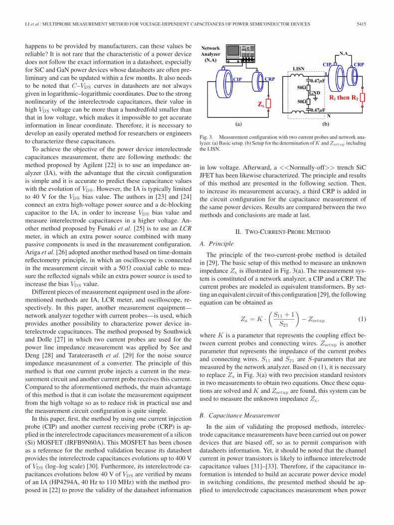
Fig. 3. Measurement configuration with two current probes and network ana-lyzer. (a) Basic setup. (b) Setup for the determination of K and Zsetup includingthe LISN.
in low voltage. Afterward, a <<Normally-off>> trench SiCJFET has been likewise characterized. The principle and resultsof this method are presented in the following section. Then,to increase its measurement accuracy, a third CRP is added inthe circuit configuration for the capacitance measurement ofthe same power devices. Results are compared between the twomethods and conclusions are made at last.
II. TWO-CURRENT-PROBE METHOD
A. Principle
The principle of the two-current-probe method is detailedin [29]. The basic setup of this method to measure an unknownimpedance Zx is illustrated in Fig. 3(a). The measurement sys-tem is constituted of a network analyzer, a CIP and a CRP. Thecurrent probes are modeled as equivalent transformers. By set-ting an equivalent circuit of this configuration [29], the followingequation can be obtained as
Zx = K ·(
S11 + 1S21
)− Zsetup (1)
where K is a parameter that represents the coupling effect be-tween current probes and connecting wires. Zsetup is anotherparameter that represents the impedance of the current probesand connecting wires. S11 and S21 are S-parameters that aremeasured by the network analyzer. Based on (1), it is necessaryto replace Zx in Fig. 3(a) with two precision standard resistorsin two measurements to obtain two equations. Once these equa-tions are solved and K and Zsetup are found, this system can beused to measure the unknown impedance Zx .
B. Capacitance Measurement
In the aim of validating the proposed methods, interelec-trode capacitance measurements have been carried out on powerdevices that are biased off, so as to permit comparison withdatasheets information. Yet, it should be noted that the channelcurrent in power transistors is likely to influence interelectrodecapacitance values [31]–[33]. Therefore, if the capacitance in-formation is intended to build an accurate power device modelin switching conditions, the presented method should be ap-plied to interelectrode capacitances measurement when power
5416 IEEE TRANSACTIONS ON POWER ELECTRONICS, VOL. 28, NO. 11, NOVEMBER 2013
Fig. 4. MOSFET interelectrode capacitances measurement by two-current-probe method. (a) Coss measurement. (b) Ciss measurement. (c) Cxmeasurement.
devices operate in linear region.The interelectrode capacitancesof the MOSFET are first measured with this method. The biasvoltage for VDS is obtained by applying an external dc powersource, of which the impedance is stabilized by a line impedancestabilization network (LISN). The impedance of the LISN maybe included in the final measurement results, in which case thedetermination of K and Zsetup [see (1)] may be obtained by theconfiguration shown in Fig. 3(b), where R1 and R2 representtwo known resistors used for obtaining two equations. The net-work analyzer Agilent E5071C (9 kHz to 4.5 GHz) is used forS-parameters measurement. FCC F-120-3 (10 kHz to 100 MHz)and FCC F35 (1 kHz to 100 MHz) are used as the CIP and CRP,respectively, while EMCO 3180/2 (9 kHz to 30 MHz) is usedas the LISN. To compare with the datasheet, the interelectrodecapacitances of the power devices are measured around 1 MHz.Below 1 MHz, the mutual inductance between two probes canbe neglected. As there are three interelectrode capacitances ofa MOSFET, this method is applied to measure the sum of twocapacitances in the following three measurements:
1) The circuit configuration used to measure Coss = Cds +Cgd is shown in Fig. 4(a). Gate and source are short cir-cuited to ensure that the MOSFET is in off state. It could
Fig. 5. Result of the Si MOSFET interelectrode capacitances measurementby two-current-probe method.
be noted that in this measurement, the impedance of theLISN is already included into Zsetup [see (1)].
2) The circuit configuration to measure Ciss = Cgs + Cgd isshown in Fig. 4(b). Gate and source of the MOSFET areshort circuited to keep it in off state. Moreover, drain andsource have to be short-circuited in ac (at 1 MHz) whilea dc bias voltage is applied between these terminals. Forthat means, an additional capacitor is connected betweendrain and source; its value (2.2 μF) is chosen so that thecapacitor impedance around 1 MHz is much smaller thanthat of both Cds and the LISN (100 Ω). Thus, the totalcapacitance measured in this configuration is
Cmeasure = Cgs +Cgd · 2.2μFCgd + 2.2μF
. (2)
Since Cgd is much smaller than 2.2 μF, Ciss is directlyobtained in this configuration.
3) The circuit configuration used to measure the sum of Cdsand Cgs (this term is called Cx = Cds + Cgs) is shown inFig. 4(c). A 2.2 μF capacitor is connected between gateand drain of the MOSFET and a resistor (R = 66 kΩ)is connected between gate and source. As Cgd is muchsmaller than 2.2μF, drain and gate are short circuited inac. The role of the resistor R is to discharge Cgs so asto keep Vgs lower than its threshold voltage (MOSFET isin off state). Furthermore, around 1 MHz, the impedanceof this resistor R is much bigger than that of Cgs whichguarantees that the injected current flows through Cgs .Similar to the Coss measurement, the impedance of theLISN is included into Zsetup . Cgd can then be obtainedindirectly by
Cgd =Ciss + Coss − Cx
2. (3)
C. Measurement Results
The results of the measured capacitances of the MOSFETcompared to the datasheet are shown in Fig. 5.
From these results, the values of Ciss and Coss in the datasheetconcur well with the values measured by applying the afore-mentioned method, so the validity of this method seems to be
LI et al.: MULTIPROBE MEASUREMENT METHOD FOR VOLTAGE-DEPENDENT CAPACITANCES OF POWER SEMICONDUCTOR DEVICES 5417
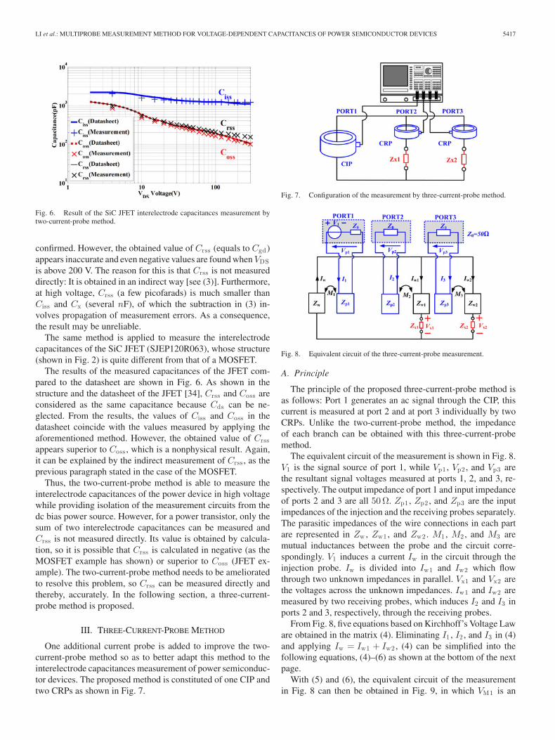
Fig. 6. Result of the SiC JFET interelectrode capacitances measurement bytwo-current-probe method.
confirmed. However, the obtained value of Crss (equals to Cgd )appears inaccurate and even negative values are found when VDSis above 200 V. The reason for this is that Crss is not measureddirectly: It is obtained in an indirect way [see (3)]. Furthermore,at high voltage, Crss (a few picofarads) is much smaller thanCiss and Cx (several nF), of which the subtraction in (3) in-volves propagation of measurement errors. As a consequence,the result may be unreliable.
The same method is applied to measure the interelectrodecapacitances of the SiC JFET (SJEP120R063), whose structure(shown in Fig. 2) is quite different from that of a MOSFET.
The results of the measured capacitances of the JFET com-pared to the datasheet are shown in Fig. 6. As shown in thestructure and the datasheet of the JFET [34], Crss and Coss areconsidered as the same capacitance because Cds can be ne-glected. From the results, the values of Ciss and Coss in thedatasheet coincide with the values measured by applying theaforementioned method. However, the obtained value of Crssappears superior to Coss , which is a nonphysical result. Again,it can be explained by the indirect measurement of Crss , as theprevious paragraph stated in the case of the MOSFET.
Thus, the two-current-probe method is able to measure theinterelectrode capacitances of the power device in high voltagewhile providing isolation of the measurement circuits from thedc bias power source. However, for a power transistor, only thesum of two interelectrode capacitances can be measured andCrss is not measured directly. Its value is obtained by calcula-tion, so it is possible that Crss is calculated in negative (as theMOSFET example has shown) or superior to Coss (JFET ex-ample). The two-current-probe method needs to be amelioratedto resolve this problem, so Crss can be measured directly andthereby, accurately. In the following section, a three-current-probe method is proposed.
III. THREE-CURRENT-PROBE METHOD
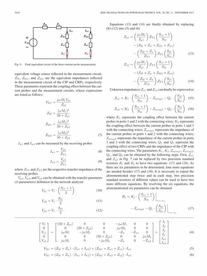
One additional current probe is added to improve the two-current-probe method so as to better adapt this method to theinterelectrode capacitances measurement of power semiconduc-tor devices. The proposed method is constituted of one CIP andtwo CRPs as shown in Fig. 7.
Fig. 7. Configuration of the measurement by three-current-probe method.
Fig. 8. Equivalent circuit of the three-current-probe measurement.
A. Principle
The principle of the proposed three-current-probe method isas follows: Port 1 generates an ac signal through the CIP, thiscurrent is measured at port 2 and at port 3 individually by twoCRPs. Unlike the two-current-probe method, the impedanceof each branch can be obtained with this three-current-probemethod.
The equivalent circuit of the measurement is shown in Fig. 8.V1 is the signal source of port 1, while Vp1 , Vp2 , and Vp3 arethe resultant signal voltages measured at ports 1, 2, and 3, re-spectively. The output impedance of port 1 and input impedanceof ports 2 and 3 are all 50Ω. Zp1 , Zp2 , and Zp3 are the inputimpedances of the injection and the receiving probes separately.The parasitic impedances of the wire connections in each partare represented in Zw , Zw1 , and Zw2 . M1 , M2 , and M3 aremutual inductances between the probe and the circuit corre-spondingly. V1 induces a current Iw in the circuit through theinjection probe. Iw is divided into Iw1 and Iw2 which flowthrough two unknown impedances in parallel. Vx1 and Vx2 arethe voltages across the unknown impedances. Iw1 and Iw2 aremeasured by two receiving probes, which induces I2 and I3 inports 2 and 3, respectively, through the receiving probes.
From Fig. 8, five equations based on Kirchhoff’s Voltage Laware obtained in the matrix (4). Eliminating I1 , I2 , and I3 in (4)and applying Iw = Iw1 + Iw2 , (4) can be simplified into thefollowing equations, (4)–(6) as shown at the bottom of the nextpage.
With (5) and (6), the equivalent circuit of the measurementin Fig. 8 can then be obtained in Fig. 9, in which VM1 is an
5418 IEEE TRANSACTIONS ON POWER ELECTRONICS, VOL. 28, NO. 11, NOVEMBER 2013
Fig. 9. Final equivalent circuit of the three-current-probe measurement.
equivalent voltage source reflected in the measurement circuit.ZM , ZM1 , and ZM2 are the equivalent impedances reflectedin the measurement circuit of the CIP and CRPs, respectively.These parameters represent the coupling effect between the cur-rent probes and the measurement circuits, whose expressionsare listed as follows:
VM1 =jωM1Vp1
Zp1
ZM =(ωM1)2
50 + Zp1
ZM1 =(ωM2)2
50 + Zp2
ZM2 =(ωM3)2
50 + Zp3. (7)
Iw1 and Iw2 can be measured by the receiving probes
Iw1 =Vp2
ZT2(8)
Iw2 =Vp3
ZT3(9)
where ZT2 and ZT3 are the respective transfer impedance of thereceiving probes.
Vp1 , Vp2 , and Vp3 can be obtained with the transfer parameter(S-parameters) definition in the network analyzer
Vp1 = V1 ·(
S11 + 12
)(10)
Vp2 = V1 ·S21
2(11)
Vp3 = V1 ·S31
2. (12)
Equations (13) and (14) are finally obtained by replacing(8)–(12) into (5) and (6)
Zx1 =(
jωM1
Zp1
)ZT2
(S11 + 1
S21
)
− (ZM + Zw + ZM1 + Zw1)
−(
ZM + Zw
ZT3
)ZT2
(S31
S21
)(13)
Zx2 =(
jωM1
Zp1
)ZT3
(S11 + 1
S31
)
− (ZM + Zw + ZM2 + Zw2)
−(
ZM + Zw
ZT2
)ZT3
(S21
S31
). (14)
Unknown impedances Zx1 and Zx2 can finally be expressed as
Zx1 = K1 ·(
S11 + 1S21
)− Zsetup1 − Q1 ·
(S31
S21
)(15)
Zx2 = K2 ·(
S11 + 1S31
)− Zsetup2 − Q2 ·
(S21
S31
)(16)
where K1 represents the coupling effect between the currentprobes in ports 1 and 2 with the connecting wires; K2 representsthe coupling effect between the current probes in ports 1 and 3with the connecting wires; Zsetup1 represents the impedance ofthe current probes in ports 1 and 2 with the connecting wires;Zsetup2 represents the impedance of the current probes in ports1 and 3 with the connecting wires; Q1 and Q2 represent thecoupling effect of two CRPs and the impedance of the CIP withthe connecting wires. The parameters K1 , K2 , Zsetup1 , Zsetup2 ,Q1 , and Q2 can be obtained by the following steps. First, Zx1and Zx2 in Fig. 7 can be replaced by two precision standardresistors R1 and R2 to have two equations: (17) and (18). Asthere are six parameters to be determined, four more equationsare needed besides (17) and (18). It is necessary to repeat theaforementioned step twice and in each step, two precisionstandard resistors of different values can be used to have twomore different equations. By resolving the six equations, theaforementioned six parameters can be obtained
R1 = K1 ·(
S11 + 1S21
) ∣∣∣∣zx 1 = R 1
− Zsetup1 − Q1 ·(
S31
S21
) ∣∣∣∣zx 1 = R 1
(17)
⎡⎢⎢⎢⎣
V10
Vx10
Vx2
⎤⎥⎥⎥⎦ =
⎡⎢⎢⎢⎣
(50 + Zp1) 0 0 −jωM1 0 00 (50 + Zp2) 0 jωM2 0 0
jωM1 −jωM2 0 −Zw −Zw1 00 0 (50 + Zp3) 0 0 jωM3
jωM1 0 −jωM3 −Zw 0 −Zw2
⎤⎥⎥⎥⎦ ×
⎡⎢⎢⎢⎢⎢⎣
I1I2I3IwIw1Iw2
⎤⎥⎥⎥⎥⎥⎦
(4)
VM1 = (ZM + Zw) · (Iw1 + Iw2) + (ZM1 + Zw1 + Zx1) · Iw1 (5)
VM1 = (ZM + Zw) · (Iw1 + Iw2) + (ZM2 + Zw2 + Zx2) · Iw2 (6)
LI et al.: MULTIPROBE MEASUREMENT METHOD FOR VOLTAGE-DEPENDENT CAPACITANCES OF POWER SEMICONDUCTOR DEVICES 5419
Fig. 10. Parameters determination of the three-current-probe method.
R2 = K2 ·(
S11 + 1S31
) ∣∣∣∣zx 2 = R 2
− Zsetup2 − Q2 ·(
S21
S31
) ∣∣∣∣zx 2 = R 2
. (18)
This three-current-probe method can be used to measure inter-electrode capacitances of the power devices in a direct manner.
B. Capacitance Measurement
Similar to what was explained in Section II-B, the presentedthree-current-probe method is applied for measuring interelec-trode capacitances when power devices are biased off, in orderto compare with datasheets information.
All the pieces of equipment, except one more receiving probewhich is EMC Test System 91550-2 (10 kHz to 150 MHz),used in this measurement are the same as presented with theaforementioned method. Similar to the two-current-probe mea-surement method, the impedance of the LISN may be includedin the final measurements, in which case the determination ofthe six parameters [see (15) and (16)] can be obtained by theconfiguration shown in Fig. 10 where R1 and R2 are chosen withthe following three groups of values: 50Ω/50Ω, 50Ω/33Ω, and33Ω/50Ω. Thus, with this configuration to determine the six pa-rameters, Zsetup1 not only represents the impedance of the cur-rent probes in ports 1 and 2 with the connecting wires, but alsothe LISN impedance; Zsetup2 not only represents the impedanceof the current probes in ports 1 and 3 with the connecting wires,but also the LISN impedance.
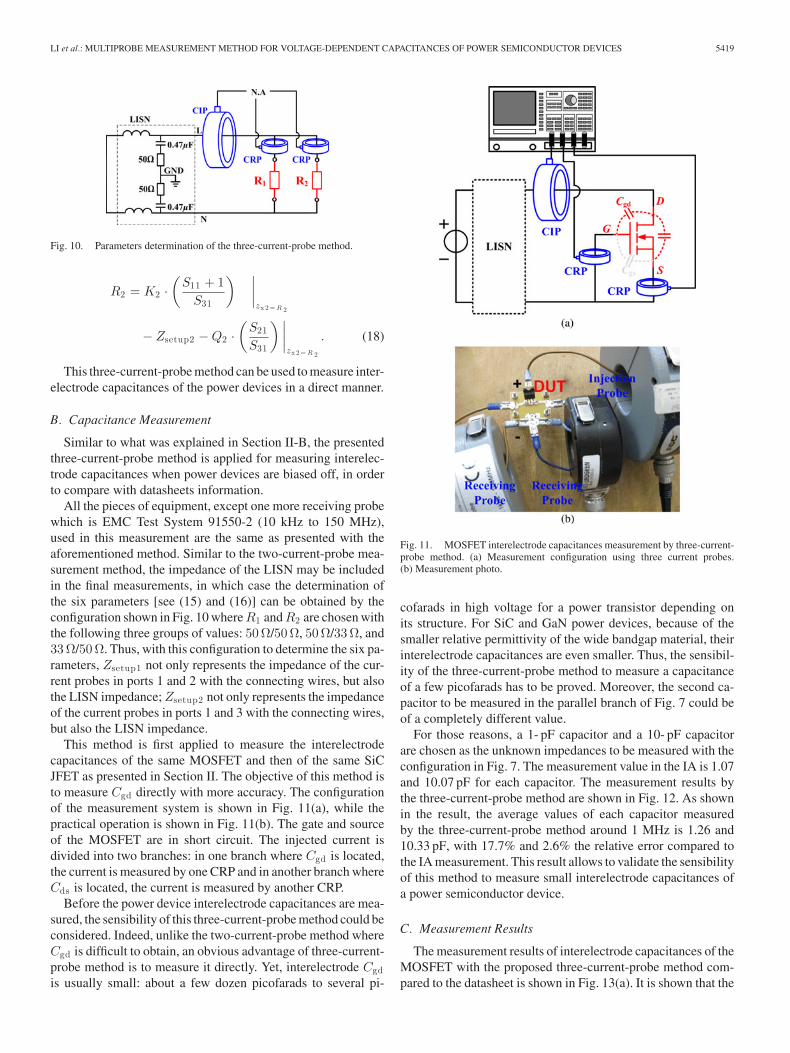
This method is first applied to measure the interelectrodecapacitances of the same MOSFET and then of the same SiCJFET as presented in Section II. The objective of this method isto measure Cgd directly with more accuracy. The configurationof the measurement system is shown in Fig. 11(a), while thepractical operation is shown in Fig. 11(b). The gate and sourceof the MOSFET are in short circuit. The injected current isdivided into two branches: in one branch where Cgd is located,the current is measured by one CRP and in another branch whereCds is located, the current is measured by another CRP.
Before the power device interelectrode capacitances are mea-sured, the sensibility of this three-current-probe method could beconsidered. Indeed, unlike the two-current-probe method whereCgd is difficult to obtain, an obvious advantage of three-current-probe method is to measure it directly. Yet, interelectrode Cgdis usually small: about a few dozen picofarads to several pi-
Fig. 11. MOSFET interelectrode capacitances measurement by three-current-probe method. (a) Measurement configuration using three current probes.(b) Measurement photo.
cofarads in high voltage for a power transistor depending onits structure. For SiC and GaN power devices, because of thesmaller relative permittivity of the wide bandgap material, theirinterelectrode capacitances are even smaller. Thus, the sensibil-ity of the three-current-probe method to measure a capacitanceof a few picofarads has to be proved. Moreover, the second ca-pacitor to be measured in the parallel branch of Fig. 7 could beof a completely different value.
For those reasons, a 1- pF capacitor and a 10- pF capacitorare chosen as the unknown impedances to be measured with theconfiguration in Fig. 7. The measurement value in the IA is 1.07and 10.07 pF for each capacitor. The measurement results bythe three-current-probe method are shown in Fig. 12. As shownin the result, the average values of each capacitor measuredby the three-current-probe method around 1 MHz is 1.26 and10.33 pF, with 17.7% and 2.6% the relative error compared tothe IA measurement. This result allows to validate the sensibilityof this method to measure small interelectrode capacitances ofa power semiconductor device.
C. Measurement Results
The measurement results of interelectrode capacitances of theMOSFET with the proposed three-current-probe method com-pared to the datasheet is shown in Fig. 13(a). It is shown that the
5420 IEEE TRANSACTIONS ON POWER ELECTRONICS, VOL. 28, NO. 11, NOVEMBER 2013
Fig. 12. Result of the 1 and 10 pF capacitor measurements.
Fig. 13. Crss measurement result by three-current-probe method. (a) MOS-FET(IRFB9N60A). (b) JFET(SJEP120R063).
measurement of Cds with three-current-probe method concurswell with the datasheet, so the validity of the three-current-probemethod can be confirmed. For this MOSFET, the two-current-probe method became inaccurate in Crss measurement whenVDS was over 30 V and even negative values appeared. Thenumerical calculation comparison between these two methodsin Crss measurement when VDS is above 30 V is shown in Ta-ble I. Three terms are compared based on the relative error (εr)
TABLE INUMERICAL CALCULATION BETWEEN TWO-CURRENT-PROBE METHOD
AND THREE-CURRENT-PROBE METHOD IN Crss MEASUREMENT
OF MOSFET (IRFB9N60A)
Fig. 14. Result of the IGBT interelectrode capacitances measurement.
between the measurement (Crss(m)) and the datasheet (Crss(d))
εr =Crss(d)−Crss(m)
Crss(d). (19)
Both the mean value εr , the standard derivation σ(εr), and themaximum absolute value |εr |(max) of this error are reported inTable I. It is to be noted that the datasheet has been chosen hereas a reference, though it remains unclear which of the datasheetor the measurement is closer to the real capacitance value in highvoltage. With three-current-probe method, as Crss is measureddirectly, negative values are avoided and the maximum errordrops from 166.0% to 24.0%. Furthermore, the three-current-probe method helps to decrease σ(εr) and |εr | (down to 7.5% and9.7%, respectively), which proves that the three-current-probemethod is more stable and accurate than the two-current-probemethod for Crss measurement.
The measurement result of Crss for the SiC JFET with thethree-current-probe method compared to the datasheet is shownin Fig. 13(b). It is shown to concur well with the datasheet,which confirms the validity of this method again. More impor-tantly, the measurement result of Crss with three-current-probemethod almost equals Coss (see Fig. 6). This reasonable resultresolves the problem in the two-current-probe measurement,which shows the accuracy of the three-current-probe method inCrss measurement.
Finally, the proposed multiprobe method is applied for thecapacitances measurement of an IGBT as shown in Fig. 14 incomparison with the datasheet as well as with a measurementusing the IA with the method proposed in [22]. As shown inthe results, the datasheet of this particular device does not coin-cide with neither IA measurement nor the proposed multiprobemeasurement. Even though the IA measurement is limited to40 V of VCE , its results up to this voltage concur well with
LI et al.: MULTIPROBE MEASUREMENT METHOD FOR VOLTAGE-DEPENDENT CAPACITANCES OF POWER SEMICONDUCTOR DEVICES 5421
the proposed multiprobe method. This result suggests that thedatasheet information should not always be blindly followed,and that proposing an effective method to measure interelec-trode capacitances is relevant in order to accurately characterizea power device. This is especially important when consideringSiC or GaN power devices whose technical data in datasheetsmay be not fully complete or subject to future revisions. In thisregard, the proposed method in this paper provides the possibil-ity to easily measure power devices interelectrode capacitancesand to compare them with other methods.
IV. CONCLUSION
This paper introduces a multiprobe method to measurevoltage-dependent interelectrode capacitances of power semi-conductor devices in high voltage. Using a simple setup, theproposed method provides the advantage of isolating differ-ent pieces of measurement equipment from the dc bias powersource. By applying a two-current-probe method in the measure-ment, the results of Ciss and Coss of a transistor are accurate, butthe result of Crss is not convincing, because of indirect calcu-lation inducing measurement errors propagation. To overcomethis inconvenient, a three-current-probe method is proposed todirectly measure Crss . Experimental results have been obtainedon several power devices of different technologies (Si MOSFETand IGBT, SiC JFET) and confirm that this method offers a pre-cise characterization of their interelectrode capacitances in highvoltage.
The measurement results could be applied to study the EMCbehavior of a power converter, as well as to model power de-vice commutation dynamics, in which case interelectrode ca-pacitances of power transistors should be measured in differentoperating conditions including linear region. Future communi-cations will focus on the use of such capacitances informationin the aim of building power device models.
REFERENCES
[1] E. Cipriano, C. Jacobina, E. da Silva, and N. Rocha, “Single-phase to three-phase power converters: State of the art,” IEEE Trans. Power Electron.,vol. 27, no. 5, pp. 2437–2452, May 2012.
[2] A. Stupar, T. Friedli, J. Minibock, and J. Kolar, “Towards a 99% efficientthree-phase buck-type PFC rectifier for 400-V dc distribution systems,”IEEE Trans. Power Electron., vol. 27, no. 4, pp. 1732–1744, Apr. 2012.
[3] R.-J. Wai, C.-Y. Lin, and B.-H. Chen, “High-efficiency dc–dc converterwith two input power sources,” IEEE Trans. Power Electron., vol. 27,no. 4, pp. 1862–1875, Apr. 2012.
[4] T.-F. Wu, Y.-D. Chang, C.-H. Chang, and J.-G. Yang, “Soft-switchingboost converter with a flyback snubber for high power applications,” IEEETrans. Power Electron., vol. 27, no. 3, pp. 1108–1119, Mar. 2012.
[5] J. Wang, H. S.-H. Chung, and R. T.-H. Li, “Characterization and exper-imental assessment of the effects of parasitic elements on the MOSFETswitching performance,” IEEE Trans. Power Electron., vol. 28, no. 1,pp. 573–590, Jan. 2013.
[6] P. Anthony, N. McNeill, and D. Holliday, “A first approach to a designmethod for resonant gate driver architectures,” IEEE Trans. Power Elec-tron., vol. 27, no. 8, pp. 3855–3868, Aug. 2012.
[7] X. Fan, T. J. Han, J. Dong, L. M. Tolbert, F. Wang. J. Nagashima,S. J. Kim, S. Kulkarni, and F. Barlow, “Development of a SiC JFET-based six-pack power module for a fully integrated inverter,” IEEE Trans.Power Electron., vol. 28, no. 3, pp. 1464–1478, Mar. 2013.
[8] D. Peftitsis, R. Baburske, J. Rabkowski, J. Lutz, G. Tolstoy, and H. Nee,“Challenges regarding parallel connection of SiC JFETs,” IEEE Trans.Power Electron., vol. 28, no. 3, pp. 1449–1463, Mar. 2013.
[9] M. Berkani, S. Lefebvre, and Z. Khatir, “Saturation current and on-resistance correlation during repetitive short-circuit conditions on SiCJFET Transistors,” IEEE Trans. Power Electron., vol. 28, no. 2, pp. 621–624, Feb. 2013.
[10] B. Hughes, J. Lazar, S. Hulsey, D. Zehnder, D. Matic, and K. Boutros,“GaN HFET switching characteristics at 350V/20A and synchronousboost converter performance at 1 MHz,” in Proc. IEEE 27th Annu. Appl.Power Electron. Conf. Expo., Feb. 2012, pp. 2506–2508.
[11] D. Peftitsis, G. Tolstoy, A. Antonopoulos, J. Rabkowski, J.-K. Lim,M. Bakowski, L. A andngquist, and H. Nee, “High-power modular multi-level converters with SiC JFETs,” IEEE Trans. Power Electron., vol. 27,no. 1, pp. 28–36, Jan. 2012.
[12] R. Wood and T. Salem, “Evaluation of a 1200-V, 800-A all-SiC dualmodule,” IEEE Trans. Power Electron., vol. 26, no. 9, pp. 2504–2511,Sep. 2011.
[13] T. Gachovska, J. L. Hudgins, A. Bryant, E. Santi, H. A. Mantooth, andA. K. Agarwal, “Modeling, simulation, and validation of a power SiCBJT,” IEEE Trans. Power Electron., vol. 27, no. 10, pp. 4338–4346, Oct.2012.
[14] B. Wrzecionko, D. Bortis, J. Biela, and J. Kolar, “Novel ac-coupled gatedriver for ultrafast switching of normally off SiC JFETs,” IEEE Trans.Power Electron., vol. 27, no. 7, pp. 3452–3463, Jul. 2012.
[15] I. Josifovic, J. Popovic-Gerber, and J. Ferreira, “Improving SiC JFETswitching behavior under influence of circuit parasitics,” IEEE Trans.Power Electron., vol. 27, no. 8, pp. 3843–3854, Aug. 2012.
[16] A. R. Hefner and Jr, D. Diebolt, “An experimentally verified IGBT modelimplemented in the Saber circuit simulator,” IEEE Trans. Power Electron.,vol. 9, no. 5, pp. 532–542, Sep. 1994.
[17] L. Jih-Sheng, H. Xudong, E. Pepa, C. Shaotang, and T. W. Nehl, “InverterEMI modeling and simulation methodologies,” IEEE Trans. Ind. Electron.,vol. 53, no. 3, pp. 736–744, Jun. 2006.
[18] N. Yang, J. Ortiz, T. Duong, A. Hefner, K. Meehan, and J.-S. Lai, “Model-ing the inter-electrode capacitances of Si CoolMOS transistors for circuitsimulation of high efficiency power systems,” in Proc. IEEE Energ. Con-vers. Congr. Expo., Sep. 2010, pp. 370–377.
[19] P. Ralston, T. Duong, N. Yang, D. Berning, C. Hood, A. Hefner, andK. Meehan, “High-voltage capacitance measurement system for SiCpower MOSFETs,” in Proc. IEEE Energ. Convers. Congr. Expo., Sep.2009, pp. 1472–1479.
[20] S. Lefebvre and F. Miserey, Composants a semi-conducteur pourl’ectronique de puissance. Paris, France: Lavoisier, 2004.
[21] E. Platania, Z. Chen, F. Chimento, A. Grekov, R. Fu, L. Lu, A. Raciti,J. Hudgins, H. Mantooth, D. Sheridan, J. Casady, and E. Santi, “A physics-based model for a SiC JFET accounting for electric-field-dependent mo-bility,” IEEE Trans. Ind. Appl., vol. 47, no. 1, pp. 199–211, Jan./Feb.2011.
[22] Agilent Impedance Measurement Handbook, 4th ed. Agilent, Santa Clara,CA, USA, 2009.
[23] Application Note AN-957 Measuring HEXFET MOSFET Characteristics.International Rectifier. (Oct. 2005). [Online]. Available: http://www.irf.com/technical-info/appnotes/an-957.pdf
[24] Z. Chen, D. Boroyevich, R. Burgos, and F. Wang, “Characterization andmodeling of 1.2 kV, 20 A SiC MOSFETs,” in Proc. IEEE Energ. Convers.Congr. Expo., Sep. 2009, pp. 1480–1487.
[25] T. Funaki, N. Phankong, T. Kimoto, and T. Hikihara, “Measuring terminalcapacitance and its voltage dependency for high-voltage power devices,”IEEE Trans. Power Electron., vol. 24, no. 6, pp. 1486–1493, Jun. 2009.
[26] Z.-N. Ariga, K. Wada, and T. Shimizu, “TDR measurement method forvoltage-dependent capacitance of power devices and components,” IEEETrans. Power Electron., vol. 27, no. 7, pp. 3444–3451, Jul. 2012.
[27] R. Southwick and W. Dolle, “Line impedance measuring instrumentationutilizing current probe coupling,” IEEE Trans. Electromagn. Compat.,vol. EMC-13, no. 4, pp. 31–36, Nov. 1971.
[28] K. Y. See and J. Deng, “Measurement of noise source impedance of SMPSusing a two probes approach,” IEEE Trans. Power Electron., vol. 19, no. 3,pp. 862–868, May 2004.
[29] V. Tarateeraseth, B. Hu, K. Y. See, and F. Canavero, “Accurate extractionof noise source impedance of an SMPS under operating conditions,” IEEETrans. Power Electron., vol. 25, no. 1, pp. 111–117, Jan. 2010.
[30] IRFB9N60A Power MOSFET. Vishay. (Mar. 2011). [Online]. Available:http://www.vishay.com/docs/91103/91103.pdf
[31] V. Hoch, J. Petzoldt, H. Jacobs, A. Schlogl, and G. Deboy, “Determinationof transient transistor capacitances of high voltage MOSFETs from dy-namic measurements,” in Proc. 21st Int. Symp. Power Semicond. DevicesIC’s, Jun. 2009, pp. 148–151.
[32] G. Verneau, L. Aubard, J.-C. Crebier, C. Schaeffer, and J.-L. Schanen,“Empirical power MOSFET modeling: Practical characterization and
5422 IEEE TRANSACTIONS ON POWER ELECTRONICS, VOL. 28, NO. 11, NOVEMBER 2013
simulation implantation,” in Proc. 37th IAS Annu. Meeting Conf. Rec.Ind. Appl., Oct. 2002, vol. 4, pp. 2425–2432.
[33] L. Aubard, G. Verneau, J. C. Crebier, C. Schaeffer, and Y. Avenas, “PowerMOSFET switching waveforms: An empirical model based on a physicalanalysis of charge locations,” in Proc. IEEE 33rd Annu. Power Electron.Spec. Conf., 2002, vol. 3, pp. 1305–1310.
[34] Normally-OFF Trench Silicon Carbide Power JFET (SJEP120R063),Rev1.4., SemiSouth Laboratories, Starkville, MS, USA, Feb. 2011.
Ke Li was born in Hangzhou, China, in 1986. Hereceived the B.E. and M.E degrees in electrical en-gineering from the Southwest Jiaotong University,Chengdu, China, in 2008 and 2011, respectively, andthe Engineering degree from the Ecole Centrale deMarseille, Marseille, France, in 2011. Since 2011, hehas been working toward the Ph.D. degree in electri-cal engineering in the Laboratory of Electrical Engi-neering and Power Electronics, University of Lille 1,France.
His current research interests include wide-bandgap (SiC/GaN) power semiconductor devices characterization and mod-eling as well as their applications in power converters.
Arnaud Videt (M’10) received the Ph.D. degree inelectrical engineering from the Ecole Centrale deLille, Lille, France, in 2008.
From 2008 to 2010, he was an R&D power elec-tronics Engineer with Schneider Toshiba Inverter,Pacy-sur-Eure, France, where his research was fo-cused on multilevel inverter control, electromagneticcompatibility (EMC), and input power quality formotor drive applications. Since 2010, he has beenworking as an Associate Professor in the Laboratoryof Electrical Engineering of Lille, Lille. His current
research interests include power quality, EMC, and wide-bandgap semiconduc-tor devices for power conversion.
Nadir Idir (M’93) received the Ph.D. degree in elec-trical engineering from the University of Lille 1, Lille,France, in 1993.
He is a Full Professor with IUT A of the Uni-versity of Lille 1, where he teaches power electron-ics and electromagnetic compatibility. Since 1993,he has been with the Laboratory of Electrical Engi-neering and Power Electronics of the University ofLille 1. His research interests include design method-ologies for HF switching converters, power devices(SiC and GaN), electromagnetic interference (EMI)
in static converters, HF modeling of the passive components, and EMI filterdesign methodologies for power converters.


![Capacitances Extraction for Multilayer Conductor ...€¦ · 2 W(er0 5) R Edxdy Fig.2. Fig.1. The per unit length capacitances of general n conductor The matrix [c] capacitance for](https://img.pdfslide.us/doc/110x75/5fd280a902280700121ed27d/capacitances-extraction-for-multilayer-conductor-2-wer0-5-r-edxdy-fig2-fig1.jpg)