Embed Size (px)
Citation preview
Multifunction counter board, optically isolated, encoder, incremental counter, timer/counter, SSI, PWM, ...
APCI-1710Available functions:
incremental counter, SSI synchronous serial
interface, counter/timer, pulse acquisition,
frequency/pulse width/period duration/velocity
measurement, PWM, digital inputs and outputs, ...
Function selection through software
Optical isolation
TTL, RS422, 24 V
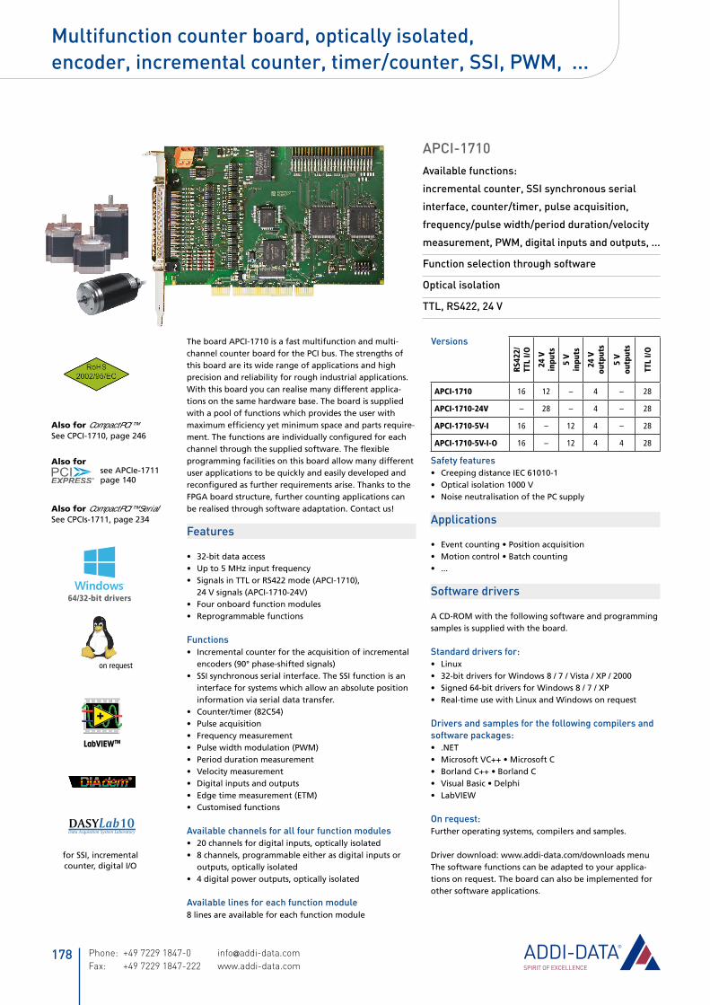
The board APCI-1710 is a fast multifunction and multi-channel counter board for the PCI bus. The strengths of this board are its wide range of applications and high precision and reliability for rough industrial applications.With this board you can realise many different applica-tions on the same hardware base. The board is supplied with a pool of functions which provides the user with maximum efficiency yet minimum space and parts require-ment. The functions are individually configured for each channel through the supplied software. The flexible programming facilities on this board allow many different user applications to be quickly and easily developed and reconfigured as further requirements arise. Thanks to the FPGA board structure, further counting applications can be realised through software adaptation. Contact us!
Features
32-bit data access• Up to 5 MHz input frequency• Signals in TTL or RS422 mode (APCI-1710), • 24 V signals (APCI-1710-24V)Four onboard function modules• Reprogrammable functions•
FunctionsIncremental counter for the acquisition of incremental • encoders (90° phase-shifted signals)SSI synchronous serial interface. The SSI function is an • interface for systems which allow an absolute position information via serial data transfer.Counter/timer (82C54)• Pulse acquisition• Frequency measurement• Pulse width modulation (PWM)• Period duration measurement• Velocity measurement• Digital inputs and outputs• Edge time measurement (ETM)• Customised functions•
Available channels for all four function modules 20 channels for digital inputs, optically isolated• 8 channels, programmable either as digital inputs or • outputs, optically isolated 4 digital power outputs, optically isolated•
Available lines for each function module8 lines are available for each function module
Versions
RS42
2/
TTL
I/O
24 V
in
puts
5 V
in
puts
24 V
ou
tput
s
5 V
ou
tput
s
TTL
I/O
APCI-1710 16 12 – 4 – 28
APCI-1710-24V – 28 – 4 – 28
APCI-1710-5V-I 16 – 12 4 – 28
APCI-1710-5V-I-O 16 – 12 4 4 28
Safety features Creeping distance IEC 61010-1• Optical isolation 1000 V• Noise neutralisation of the PC supply•
Applications
Event counting • Position acquisition• Motion control • Batch counting• ...•
Software drivers
A CD-ROM with the following software and programming samples is supplied with the board.
Standard drivers for:Linux• 32-bit drivers for Windows 8 / 7 / Vista / XP / 2000• Signed 64-bit drivers for Windows 8 / 7 / XP• Real-time use with Linux and Windows on request•
Drivers and samples for the following compilers and software packages:
.NET• Microsoft VC++ • Microsoft C• Borland C++ • Borland C• Visual Basic • Delphi• LabVIEW•
On request:Further operating systems, compilers and samples.
Driver download: www.addi-data.com/downloads menuThe software functions can be adapted to your applica-tions on request. The board can also be implemented for other software applications.
Also for CompactPCI™ See CPCI-1710, page 246
Also for CompactPCI™ Serial See CPCIs-1711, page 234
Also for see APCIe-1711
page 140
for SSI, incremental counter, digital I/O
LabVIEWTM
64/32-bit drivers
on request
Phone: +49 7229 1847-0 [email protected] Fax: +49 7229 1847-222 www.addi-data.com
178
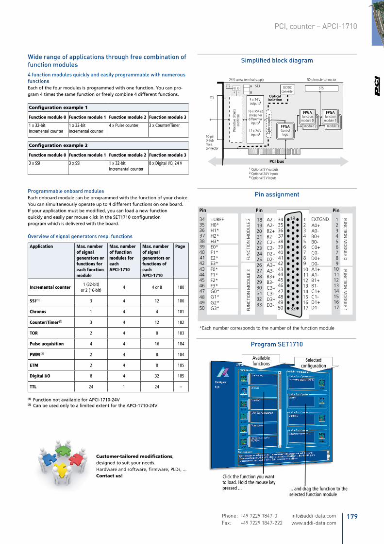
Wide range of applications through free combination of function modules4 function modules quickly and easily programmable with numerous functionsEach of the four modules is programmed with one function. You can pro-gram 4 times the same function or freely combine 4 different functions.
Configuration example 1
Function module 0 Function module 1 Function module 2 Function module 3
1 x 32-bit Incremental counter
1 x 32-bit Incremental counter
4 x Pulse counter 3 x Counter/Timer
Configuration example 2
Function module 0 Function module 1 Function module 2 Function module 3
3 x SSI 3 x SSI 1 x 32-bit Incremental counter
8 x Digital I/O, 24 V
Programmable onboard modulesEach onboard module can be programmed with the function of your choice. You can simultaneously operate up to 4 different functions on one board.If your application must be modified, you can load a new function quickly and easily per mouse click in the SET1710 configuration program which is delivered with the board.
Overview of signal generators resp. functions
Application Max. number of signal generators or functio ns for each function module
Max. number of function modules for each APCI-1710
Max. number of signal generators or functions of each APCI-1710
Page
Incremental counter1 (32-bit)
or 2 (16-bit)4 4 or 8 180
SSI [1] 3 4 12 180
Chronos 1 4 4 181
Counter/Timer [2] 3 4 12 182
TOR 2 4 8 183
Pulse acquisition 4 4 16 184
PWM [2] 2 4 8 184
ETM 2 4 8 185
Digital I/O 8 4 32 185
TTL 24 1 24 –
[1] Function not available for APCI-1710-24V[2] Can be used only to a limited extent for the APCI-1710-24V
Pin assignment
123456789
+UREFH0*H1*H2*H3*
F0*F1*F2*F3*G0*G1*G2*G3*
E0*E1*E2*E3*
A2+A2-B2+B2-C2+C2-D2+D2-A3+A3-B3+B3-C3+C3-D3+D3-
A0+A0-B0+B0-C0+C0-D0+D0-A1+A1-B1+B1-C1+C1-D1+D1-
3435363738394041424344454647484950
18192021222324252627282930313233
3435363738394041424344454647484950
123456789
1011121314151617
18
33
Pin PinPin
FUN
CTI
ON
MO
DU
LE 3
FUN
CTI
ON
MO
DU
LE 2
1011121314151617
FUN
CTIO
N M
OD
ULE 1
FUN
CTIO
N M
OD
ULE 0
EXTGND
*Each number corresponds to the number of the function module
Click the function you want to load. Hold the mouse key pressed ... ... and drag the function to the
selected function module
Available functions
Selectedconfiguration
Customer-tailored modifications,designed to suit your needs. Hardware and software, firmware, PLDs, ...Contact us!
24 V screw terminal supply 50-pin male connector
50-pinD-Submaleconnector
PCI bus
Opticalisolation
DC/DCconverter
Prot
ectiv
e cir
cuits
an
d fil
ters
4 x 24 V outputs1
16 x RS422drivers fordifferential
inputs2
12 x 24 V inputs3
1 Optional 5 V outputs2 Optional 24 V inputs3 Optional 5 V inputs
ST1
ST2 ST3A
BST5
FPGAControllogic
FPGAfunktionmodule 2
FPGAfunktionmodule 3
FPGAfunctionmodule 0
FPGAfunctionmodule 1
Opt
o-co
uple
rs
Simplified block diagram
Program SET1710
179Phone: +49 7229 1847-0 [email protected] Fax: +49 7229 1847-222 www.addi-data.com
PCI, counter – APCI-1710
Used signals
Signal Pin name name Signal type FunctionA_x Ax +/- Diff./TTL/24 V* Trace A of the incremental encoder (32-bit) or Trace A of the incremental encoder 0 (16-bit)
B_x Bx +/- Diff./TTL/24 V* Trace B of the incremental encoder (32-bit) or Trace B of the incremental encoder 0 (16-bit)
INDEX_x Cx +/- Diff./TTL/24 V* Index trace of the incremental encoder (32-bit)
C_x Cx +/- Diff./TTL/24 V* Trace A of the incremental encoder 1 (2x16-bit)
UAS_x Dx +/- Diff./TTL/24 V* Error signal input (32-bit)
D_x Dx +/- Diff./TTL/24 V* B signal of the incremental encoder 1 (2x16-bit)
REF_x Ex 24 V / optional 5 V Digital input (can also control the reference point logic)
ExtStrb_a_x Fx 24 V / optional 5 V Digital input Active High (can be used for the latch logic or interrupt logic)
ExtStrb_b_x Gx 24 V / optional 5 V Digital input Active High (can be used for latch logic or interrupt logic)
DIG_OUT_x Hx 24 V / optional 5 V Digital output
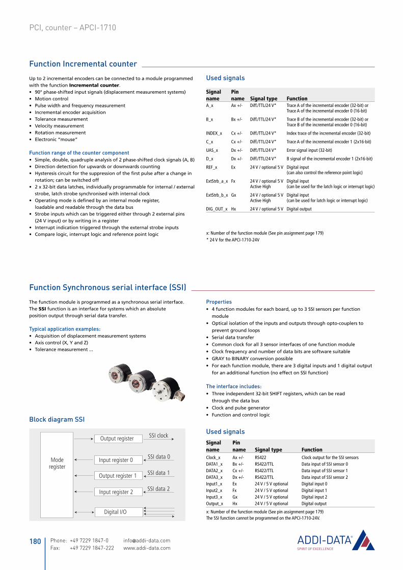
Function Incremental counter
Function Synchronous serial interface (SSI)
The function module is programmed as a synchronous serial interface.The SSI function is an interface for systems which an absolute po sition output through serial data transfer.
Typical application examples: Acquisition of displacement measurement systems• Axis control (X, Y and Z)• Tolerance measurement ...•
Moderegister
Output register
Input register 0
Output register 1
Input register 2
Digital I/O
SSI clock
SSI data 0
SSI data 2
SSI data 1
Up to 2 incremental encoders can be connected to a module programmed with the function Incremental counter.
90° phase-shifted input signals (displacement measurement systems)• Motion control• Pulse width and frequency measurement• Incremental encoder acquisition• Tolerance measurement• Velocity measurement• Rotation measurement• Electronic “mouse”•
Function range of the counter componentSimple, double, quadruple analysis of 2 phase-shifted clock signals (A, B) • Direction detection for upwards or downwards counting• Hysteresis circuit for the suppression of the first pulse after a change in • rotation; can be switched off2 x 32-bit data latches, individually programmable for internal / external • strobe, latch strobe synchronised with internal clockOperating mode is defined by an internal mode register, • loadable and readable through the data busStrobe inputs which can be triggered either through 2 external pins • (24 V input) or by writing in a registerInterrupt indication triggered through the external strobe inputs• Compare logic, interrupt logic and reference point logic•
Properties4 function modules for each board, up to 3 SSI sensors per function •
module
Optical isolation of the inputs and outputs through opto-couplers to •
prevent ground loops
Serial data transfer•
Common clock for all 3 sensor interfaces of one function module•
Clock frequency and number of data bits are software suitable•
GRAY to BINARY conversion possible•
For each function module, there are 3 digital inputs and 1 digital output •
for an additional function (no effect on SSI function)
The interface includes:Three independent 32-bit SHIFT registers, which can be read •
through the data bus
Clock and pulse generator•
Function and control logic •
Used signalsSignal Pin name name Signal type FunctionClock_x Ax +/- RS422 Clock output for the SSI sensorsDATA1_x Bx +/- RS422/TTL Data input of SSI sensor 0DATA2_x Cx +/- RS422/TTL Data input of SSI sensor 1DATA3_x Dx +/- RS422/TTL Data input of SSI sensor 2Input1_x Ex 24 V / 5 V optional Digital input 0Input2_x Fx 24 V / 5 V optional Digital input 1Input3_x Gx 24 V / 5 V optional Digital input 2Output_x Hx 24 V / 5 V optional Digital output
Block diagram SSI
x: Number of the function module (See pin assignment page 179) * 24 V for the APCI-1710-24V
x: Number of the function module (See pin assignment page 179)The SSI function cannot be programmed on the APCI-1710-24V.
Phone: +49 7229 1847-0 [email protected] Fax: +49 7229 1847-222 www.addi-data.com
180
PCI, counter – APCI-1710
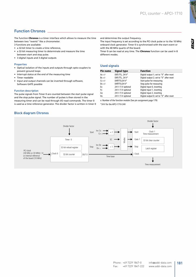
Function Chronos
The function Chronos is a timer interface which allows to measure the time between two “events” like a chronometer. 3 functions are available:
a 32-bit timer to create a time reference,• a 32-bit measuring timer to determinate and measure the time • between start and stop pulse. 3 digital inputs and 3 digital outputs•
PropertiesOptical isolation of the inputs and outputs through opto-couplers to • prevent ground loopsInterrupt status at the end of the measuring time• Timer readable• Input and output channels can be inverted through software, • Software GATE possible
Function descriptionThe pulse signals from Timer 0 are counted between the start pulse signal and the stop pulse signal. The number of pulses is then stored in the measuring timer and can be read through I/O read commands. The timer 0 is used as a time reference generator. The divider factor is written in timer 0
32-bit counter
32-bit reload register
Divider factor
PCI clock (30 MHz or 33 MHz)
Time base
32-bit clear counter
Time measurement
Divider factor
Time measurement
or internal referenceof the board (10 MHz)
Timer 0
/ 4 Clock 0 OUT 0
Latch register
Clock 1
Clock
Stop
Gate 1
Start
Mod
es
= 1
= 1
SC
Start
Stop
Inc Cx
Inc Dx
Cx
Dx
and determines the output frequency.The input frequency is set according to the PCI clock pulse or to the 10 MHz onboard clock generator. Timer 0 is synchronised with the start event or with the 40 MHz quartz of the board.Timer 0 can be read at any time. The Chronos function can be used in 8 different modes.
Used signalsPin name Signal type FunctionAx +/- Diff./TTL, 24 V* Digital output 1; set to “0” after resetBx +/- Diff./TTL, 24 V* Digital output 2; set to “0” after resetCx +/- Diff/TTL/24 V* Start pulse for measuringDx +/- Diff/TTL/24 V* Stop pulse for measuringEx 24 V / 5 V optional Digital input 0, invertingFx 24 V / 5 V optional Digital input 1, invertingGx 24 V / 5 V optional Digital input 2, invertingHx 24 V / 5 V optional Digital output 0; set to “0” after reset
Block diagram Chronos
x: Number of the function module (See pin assignment page 179)
*24 V for the APCI-1710-24V
181Phone: +49 7229 1847-0 [email protected] Fax: +49 7229 1847-222 www.addi-data.com
PCI, counter – APCI-1710
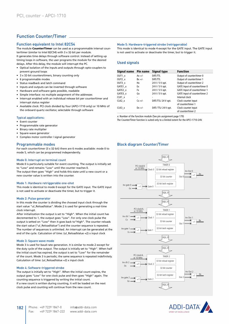
Function Counter/Timer
Function equivalent to Intel 82C54The module Counter/Timer can be used as a programmable interval coun-ter/timer (similar to Intel 82C54) with 3 x 32-bit per module. It generates time delays through software control. Instead of setting up timing loops in software, the user programs the module for the desired delays. After this delay, the module will interrupt the PC.
Optical isolation of the inputs and outputs through opto-couplers to • prevent ground loops3 x 32-bit counters/timers, binary counting only• 6 programmable modes• Status readback and latch command• Inputs and outputs can be inverted through software• Hardware and software gate possible, readable• Simple interface: no multiple assignment of the addresses• Interrupt enabled with an individual release bit per counter/timer and • interrupt status registerAvailable clock: PCI clock divided by four (APCI-1710 only) or 10 MHz of • the onboard quartz oscillator, selectable through software
Typical applications:Event counter• Programmable rate generator• Binary rate multiplier• Square-wave generator • Complex motor controller / signal generator•
Programmable modesFor each counter/timer (3 x 32-bit) there are 6 modes available: mode 0 to mode 5, which can be programmed independently.
Mode 0: Interrupt on terminal countMode 0 is particularly suitable for event counting. The output is initially set to “Low” and remains “Low” until the counter reaches 0. The output then goes “High” and holds this state until a new count or a new counter value is written into the counter.
Mode 1: Hardware retriggerable one-shotThis mode is identical to mode 0 except for the GATE input. The GATE input is not used to activate or deactivate the timer, but to trigger it.
Mode 2: Pulse generatorIn this mode the counter is dividing the choosed input clock through the start value “ul_ReloadValue”. Mode 2 is used for generating a real-time clock interrupt. After initialization the output is set to “High”. When the initial count has decremented to 1, the output goes “Low”. For only one clock pulse the output is setted on “Low” then it goes back to“High”. The counter reloads the start value (“ul_ReloadValue”) and the counter sequence is repeated. The number of sequences is unlimited. An interrupt can be generated at the end of the cycle. Calculation of time: (ul_ReloadValue +2) x input clock
Mode 3: Square wave modeMode 3 is used for baud rate generation. It is similar to mode 2 except for the duty cycle of the output. The output is initially set to “High”. When half the initial count has expired, the output is set to “Low” for the remainder of the count. Mode 3 is periodic; the same sequence is repeated indefinitely. Calculation of time: (ul_ReloadValue +2) x input clock
Mode 4: Software-triggered strobeThe output is initially set to “High”. When the initial count expires, the output goes “Low” for one clock pulse and then goes “High” again. The counting sequence is triggered by writing the initial count.If a new count is written during counting, it will be loaded on the next clock pulse and counting will continue from the new count.
Clock 0
Gate 0
Out 0
PCI clock/4or 10 MHz
Inv gate 0
-Ex
Inv Out 0Ax
TIMER 0
DQ0..31
PCI clock/4,or 10 MHz
Clock 1
Gate 1Inv gate 1
Fx
Inv clk 1 Inv Out 1BxCx
Out 1
TIMER 1
PCI clock/4,or 10 MHz
Clock 2
Gate 2Out 2Inv gate 2
Gx
Inv clk 2
Inv Out 2Hx
TIMER 2
Dx
DQ0..31
DQ0..31
DQ0..31
DQ0..31
DQ0..31
32-bit reload register
32-bit counter
32-bit latch register
32-bit reload register
32-bit counter
32-bit latch register
32-bit reload register
32-bit counter
32-bit latch register
=1
=1
=1
=1
=1
=1
=1
=1
Mode 5: Hardware-triggered strobe (retriggerable)This mode is identical to mode 4 except for the GATE input. The GATE input is not used to activate or deactivate the timer, but to trigger it.
Used signals
Signal name Pin name Signal type FunctionOUT1_x Ax +/- Diff./TTL Output of counter/timer 0OUT2_x Bx +/- Diff./TTL Output of counter/timer 1OUT3_x Hx 24 V / 5 V opt. Output of counter/timer 2GATE1_x Ex 24 V / 5 V opt. GATE Input of counter/timer 0GATE2_x Fx 24 V / 5 V opt. GATE Input of counter/timer 1GATE3_x Gx 24 V / 5 V opt. GATE Input of counter/timer 2CLK1_x - - Internal clock CLK2_x Cx +/- Diff./TTL/ 24 V opt. Clock counter input of counter/timer 1CLK3_x Dx +/- Diff./ TTL/ 24 V opt. Clock counter input of counter/timer 2
The Counter/Timer function is suited only to a limited extent for the APCI-1710-24V.
Block diagram Counter/Timer
x: Number of the function module (See pin assignment page 179)
Phone: +49 7229 1847-0 [email protected] Fax: +49 7229 1847-222 www.addi-data.com
182
PCI, counter – APCI-1710
Block diagram TOR
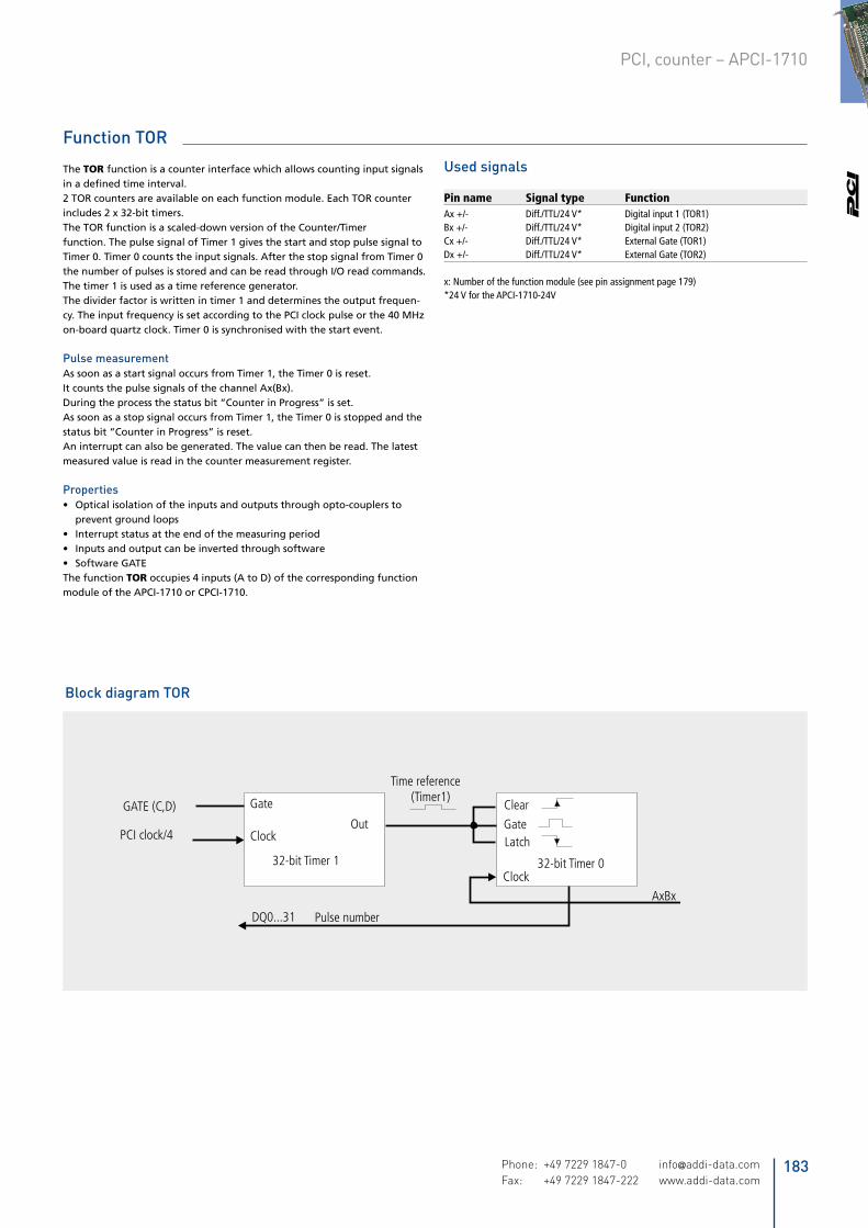
Function TOR
The TOR function is a counter interface which allows counting input signals in a defined time interval.2 TOR counters are available on each function module. Each TOR counter includes 2 x 32-bit timers.The TOR function is a scaled-down version of the Counter/Timer function. The pulse signal of Timer 1 gives the start and stop pulse signal to Timer 0. Timer 0 counts the input signals. After the stop signal from Timer 0 the number of pulses is stored and can be read through I/O read commands.The timer 1 is used as a time reference generator. The divider factor is written in timer 1 and determines the output frequen-cy. The input frequency is set according to the PCI clock pulse or the 40 MHz on-board quartz clock. Timer 0 is synchronised with the start event.
Pulse measurementAs soon as a start signal occurs from Timer 1, the Timer 0 is reset. It counts the pulse signals of the channel Ax(Bx). During the process the status bit “Counter in Progress” is set.As soon as a stop signal occurs from Timer 1, the Timer 0 is stopped and the status bit “Counter in Progress” is reset. An interrupt can also be generated. The value can then be read. The latest measured value is read in the counter measurement register.
PropertiesOptical isolation of the inputs and outputs through opto-couplers to • prevent ground loopsInterrupt status at the end of the measuring period• Inputs and output can be inverted through software• Software GATE•
The function TOR occupies 4 inputs (A to D) of the corresponding function module of the APCI-1710 or CPCI-1710.
Used signals
Pin name Signal type FunctionAx +/- Diff./TTL/24 V* Digital input 1 (TOR1)Bx +/- Diff./TTL/24 V* Digital input 2 (TOR2)Cx +/- Diff./TTL/24 V* External Gate (TOR1)Dx +/- Diff./TTL/24 V* External Gate (TOR2)
x: Number of the function module (see pin assignment page 179)*24 V for the APCI-1710-24V
183Phone: +49 7229 1847-0 [email protected] Fax: +49 7229 1847-222 www.addi-data.com
PCI, counter – APCI-1710
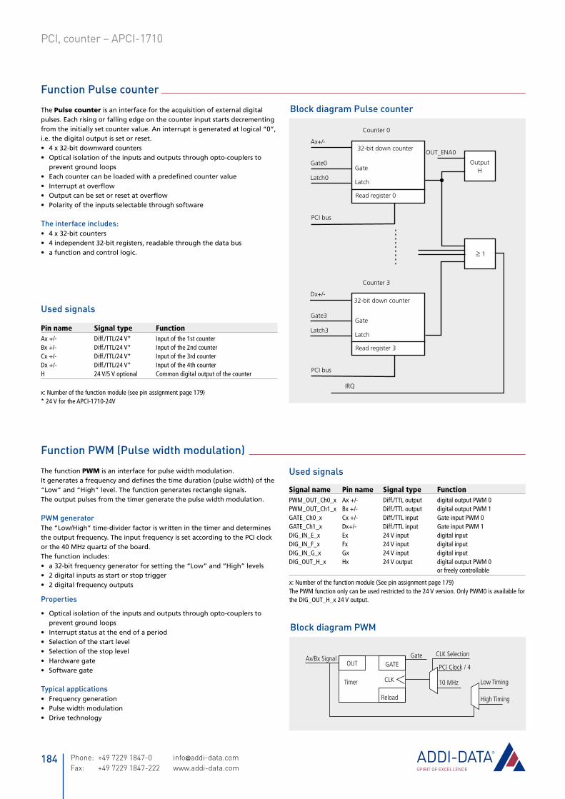
Function Pulse counter
The Pulse counter is an interface for the acquisition of external digital pulses. Each rising or falling edge on the counter input starts decrementing from the initially set counter value. An interrupt is generated at logical “0”, i.e. the digital output is set or reset.
4 x 32-bit downward counters• Optical isolation of the inputs and outputs through opto-couplers to • prevent ground loopsEach counter can be loaded with a predefined counter value• Interrupt at overflow• Output can be set or reset at overflow• Polarity of the inputs selectable through software •
The interface includes:4 x 32-bit counters• 4 independent 32-bit registers, readable through the data bus• a function and control logic.•
Used signals
Pin name Signal type FunctionAx +/- Diff./TTL/24 V* Input of the 1st counterBx +/- Diff./TTL/24 V* Input of the 2nd counterCx +/- Diff./TTL/24 V* Input of the 3rd counterDx +/- Diff./TTL/24 V* Input of the 4th counterH 24 V/5 V optional Common digital output of the counter
x: Number of the function module (see pin assignment page 179)* 24 V for the APCI-1710-24V
Function PWM (Pulse width modulation)
The function PWM is an interface for pulse width modulation. It generates a frequency and defines the time duration (pulse width) of the “Low” and “High” level. The function generates rectangle signals.The output pulses from the timer generate the pulse width modulation.
PWM generatorThe “Low/High” time-divider factor is written in the timer and determines the output frequency. The input frequency is set according to the PCI clock or the 40 MHz quartz of the board.The function includes:
a 32-bit frequency generator for setting the “Low” and “High” levels• 2 digital inputs as start or stop trigger• 2 digital frequency outputs•
Properties
Optical isolation of the inputs and outputs through opto-couplers to • prevent ground loopsInterrupt status at the end of a period• Selection of the start level• Selection of the stop level• Hardware gate• Software gate•
Typical applications Frequency generation• Pulse width modulation• Drive technology•
Block diagram PWM
Ax/Bx SignalOUT GATE
CLKTimer
Reload
Gate CLK Selection
PCI Clock / 4
10 MHz Low Timing
High Timing
Block diagram Pulse counter
Used signals
Signal name Pin name Signal type FunctionPWM_OUT_Ch0_x Ax +/- Diff./TTL output digital output PWM 0PWM_OUT_Ch1_x Bx +/- Diff./TTL output digital output PWM 1GATE_Ch0_x Cx +/- Diff./TTL input Gate input PWM 0GATE_Ch1_x Dx+/- Diff./TTL input Gate input PWM 1DIG_IN_E_x Ex 24 V input digital inputDIG_IN_F_x Fx 24 V input digital inputDIG_IN_G_x Gx 24 V input digital inputDIG_OUT_H_x Hx 24 V output digital output PWM 0 or freely controllable
x: Number of the function module (See pin assignment page 179)The PWM function only can be used restricted to the 24 V version. Only PWM0 is available for the DIG_OUT_H_x 24 V output.
Phone: +49 7229 1847-0 [email protected] Fax: +49 7229 1847-222 www.addi-data.com
184
PCI, counter – APCI-1710
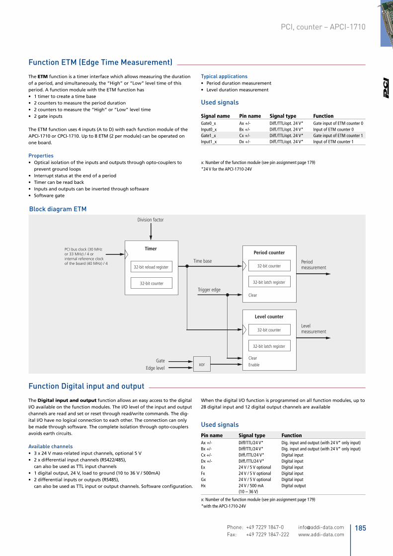
Function Digital input and output
The Digital input and output function allows an easy access to the digital I/O available on the function modules. The I/O level of the input and output channels are read and set or reset through read/write commands. The dig-ital I/O have no logical connection to each other. The connection can only be made through software. The complete isolation through opto-couplers avoids earth circuits.
Available channels3 x 24 V mass-related input channels, optional 5 V• 2 x differential input channels (RS422/485), • can also be used as TTL input channels1 digital output, 24 V, load to ground (10 to 36 V / 500mA)• 2 differential inputs or outputs (RS485), • can also be used as TTL input or output channels. Software configuration.
Function ETM (Edge Time Measurement)
The ETM function is a timer interface which allows measuring the duration of a period, and simultaneously, the “High” or “Low” level time of this period. A function module with the ETM function has
1 timer to create a time base• 2 counters to measure the period duration• 2 counters to measure the “High” or “Low” level time• 2 gate inputs•
The ETM function uses 4 inputs (A to D) with each function module of the APCI-1710 or CPCI-1710. Up to 8 ETM (2 per module) can be operated on one board.
PropertiesOptical isolation of the inputs and outputs through opto-couplers to • prevent ground loopsInterrupt status at the end of a period• Timer can be read back• Inputs and outputs can be inverted through software• Software gate•
Block diagram ETM
xorGate
Trigger edge
Time base
Edge level
32-bit reload register
32-bit counter
Timer
Division factor
32-bit counter
32-bit latch register
Period counter
Clear
32-bit counter
32-bit latch register
Level counter
Clear
Enable
Periodmeasurement
Levelmeasurement
PCI bus clock (30 MHzor 33 MHz) / 4 orinternal reference clockof the board (40 MHz) / 4
Typical applicationsPeriod duration measurement• Level duration measurement•
Used signals
Signal name Pin name Signal type FunctionGate0_x Ax +/- Diff./TTL/opt. 24 V* Gate input of ETM counter 0Input0_x Bx +/- Diff./TTL/opt. 24 V* Input of ETM counter 0Gate1_x Cx +/- Diff./TTL/opt. 24 V* Gate input of ETM counter 1Input1_x Dx +/- Diff./TTL/opt. 24 V* Input of ETM counter 1
When the digital I/O function is programmed on all function modules, up to 28 digital input and 12 digital output channels are available
Used signalsPin name Signal type FunctionAx +/- Diff/TTL/24 V* Dig. input and output (with 24 V* only input)Bx +/- Diff/TTL/24 V* Dig. input and output (with 24 V* only input)Cx +/- Diff./TTL/24 V* Digital inputDx +/- Diff./TTL/24 V* Digital inputEx 24 V / 5 V optional Digital inputFx 24 V / 5 V optional Digital inputGx 24 V / 5 V optional Digital inputHx 24 V / 500 mA Digital output (10 – 36 V)
x: Number of the function module (see pin assignment page 179)*24 V for the APCI-1710-24V
x: Number of the function module (see pin assignment page 179)*with the APCI-1710-24V
185Phone: +49 7229 1847-0 [email protected] Fax: +49 7229 1847-222 www.addi-data.com
PCI, counter – APCI-1710
Specifications
Ordering information
Counter components Counting depth: 32-bit, Counting frequency: up to 5 MHz
Free programming of the functions 32-bit or 16-bit acquisition of incremental encoders Acquisition of absolute encoders/SSI Counter/timer Chronos/TOR for frequency measurement Pulse acquisition Chronos for pulse width modulation Chronos for period duration measurement TOR for velocity measurement Digital I/O, 24 V, TTL, RS422 PWM ETM Customised functions
Signals Digital I/O signals, TTL or RS422
InputsNumber of inputs: 20Differential inputs or outputs 5 V inputs: 8/16 (8 can be used as inputs or outputs)Nominal voltage: 5 VDCCommon mode range: +12 / –7 VMax. differential voltage ±12 VInput sensitivity: 200 mVInput hysteresis: 50 mVInput impedance: 12 kΩTerminal resistor: 150 Ω serial with 10 nF (typ.) Signal delay: 120 nS (at nominal voltage)Max. input frequency: 2.5 MHz (at nominal voltage)Mass-related inputs, 24 V (channels E, F, G): Number of inputs: 12Nominal voltage: 24 VDCInput current: 11 mA (typical) at nominal voltageLogic input levels: Unominal: 24 V UH max.: 30 V UH min.: 19 V UL max.: 15 V UL min.: 0 VSignal delay: 120 ns (at nominal voltage)Maximal input frequency: 1 MHz
OutputsNominal voltage: 5 VDCMaximum output frequency: 2.5 MHz (diff. outputs)Max. number of outputs: 8 (if they are not used as diff. inputs)Digital outputs, 24 V: Output type: High-side (load to ground)Number of outputs: 4Nominal voltage: 24 VDCRange of the supply voltage: 10 V to 36 VDC (via 24 V ext. pin)Maximum current for 4 outputs: 2 A typ. (limited to the voltage supply)Maximum output current: 500 mA short-circuit current/ output at 24 V, Rload < 0.1 Ω: 1.5 A max. (output switches off)ON-resistance of the output (RDS ON resistance): 0.4 Ω max.
Overtemperature: 170 °C (all outputs switch off)Overtemperature protection (24 V outputs) Activated: From approx. 150-170 °C (chip temperature) Deactivated (automatically): From approx. 125-140 °C (chip temperature)Outputs (at overtemperature): Outputs switch offProtection against undervoltage (effective at V ext.<5 V): Outputs (at undervoltage): All outputs switch offSwitching characteristics of the 24 V outputs (V ext. = 24 V, T=25 °C, ohmic load: 500 mA): Switch ON time: 200 µs Switch OFF time: 15 µsDigital outputs, 5 V (option): Output type: TTLNumber of outputs: 4Nominal voltage: 5 VDCSwitching characteristics of the 5 V outputs (T=25 °C, TTL load): Switch ON time: 0.06 µs Switch OFF time: 0.02 µsTechnical data for the APCI-1710-24 V board version 24 V inputs (channels A to G). This board version is exclusively used for connecting 24 V encoders. Only 24 V signals can be connected to the input channels.Nominal voltage: 24 VDC / 10 mAMax. input frequency: 1 MHz (at nominal voltage)Logic input levels : U nominal: 24 V (Standard) UH max.: 30 V UH min.: 19 V UL max.: 15 V UL min.: 0 V
SafetyOptical isolation: 1000 V
EMC – Electromagnetic compatibilityThe product complies with the European EMC directive. The tests were carried out by a certified EMC laboratory in accordance with the norm from the EN 61326 series (IEC 61326). The limit values as set out by the European EMC directive for an industrial environment are complied with. The respective EMC test report is available on request.
Physical and environmental conditionsDimensions: 179 x 99 mmSystem bus: PCI 32-bit 5 V acc. to specification 2.1 (PCISIG)Space required: 1 slotOperating voltage: +5 V, ± 5 % from the PC +24 V ext. /10 mA Current consumption: APCI-1710-x: 1.15 A typ. ± 10 % Front connector: 50-pin D-Sub male connectorAdditional connector: Male connector for the TTL I/O functionTemperature range: 0 to 60 °C (with forced cooling)
OptionOpt. 5V: 5 V outputs instead of 24 V (H0, H1, H2, H3)
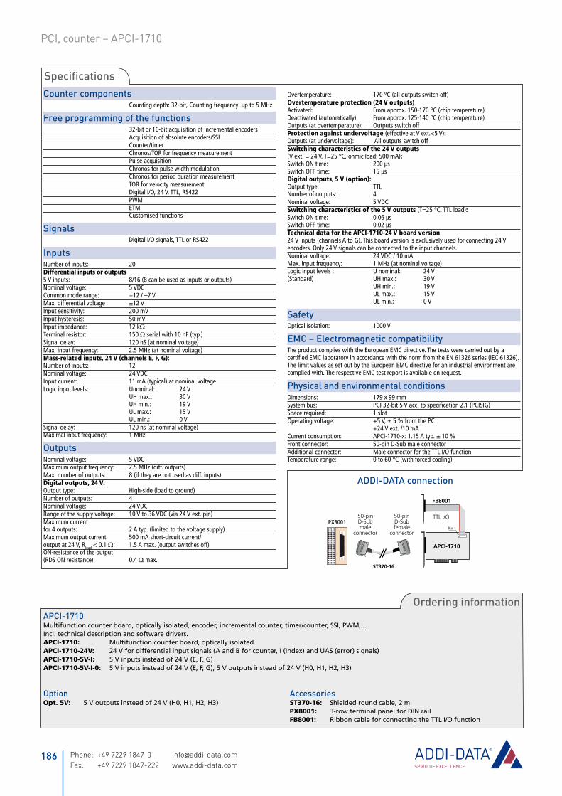
AccessoriesST370-16: Shielded round cable, 2 mPX8001: 3-row terminal panel for DIN railFB8001: Ribbon cable for connecting the TTL I/O function
APCI-1710 Multifunction counter board, optically isolated, encoder, incremental counter, timer/counter, SSI, PWM,... Incl. technical description and software drivers.APCI-1710: Multifunction counter board, optically isolatedAPCI-1710-24V: 24 V for differential input signals (A and B for counter, I (Index) and UAS (error) signals)APCI-1710-5V-I: 5 V inputs instead of 24 V (E, F, G)APCI-1710-5V-I-0: 5 V inputs instead of 24 V (E, F, G), 5 V outputs instead of 24 V (H0, H1, H2, H3)
APCI-1710
ST370-16
FB8001
TTL I/OPX8001
50-pinD-Subfemale
connector
50-pinD-Submale
connectorPin 1
ADDI-DATA connection
Phone: +49 7229 1847-0 [email protected] Fax: +49 7229 1847-222 www.addi-data.com
186
PCI, counter – APCI-1710