Embed Size (px)
Citation preview
strip is used to generate the low frequency resonance. It is clearthat the physical length can be reduced by up to 50% because thedriven plate and shorted parasitic strip are folded. The total length[l1 � l2 � gap (0.2 mm)] is 15.2 mm, which is about �0/4 of 2.4GHz. To get the dual band operation, the optimum length of eachplate and the gap between two plates are determined based on thesimulation result shown in Figure 2. In addition to the plate lengthand gap, the size of ground plane also affects the electrical per-formance. The feeding point is on the driven plate and 3 mm apartfrom the ground post, as shown in Figure 1. The radiating plate is7 mm in length and 0.5 mm in width and normally generates aresonance of 5.3 GHz band. And the shorted parasitic strip pro-duces the other resonance in 2.4 GHz. None of the dimensionsaforementioned are optimized in the specific unit.
Figure 1(b) shows a folded loop antenna with a parasitic foldedshorted-strip. In recent years, a monopole antenna has been themost promising candidate for mobile communications. However,because of compact mobile devices, a protuberant element is nolonger a possible solution. The folded loop shown in Figure 1(b)could satisfy both size and performance issues. Figure 2 presentsthe return loss of the simulation and measurement and shows fairlygood performance in both frequency bands. Two antennas havealmost the same bandwidth in the 2.4 GHz band, but the foldedloop type has more bandwidth in the 5 GHz band. Figure 3 showsthe measured radiation patterns in the x–y plane. The results areEtot (E� � E�), which is generally adopted in commercial speci-fications. The measured average gain in the 2.4 and 5 GHz bandhave a level of approximately �2 dBi for the inverted-F andapproximately �1 dBi for the folded loop, respectively. Thismeets the typical specifications of most of the wireless applica-tions. It should be emphasized that the main reason why we presentthe folded loop type here is to get the uniform radiation pattern inthe x–y plane. As shown in Figure 3(a), the inverted-F type haspoor directivity gain in the x direction (� � 90°). On the otherhand, the folded loop type has good radiation performance in alldirections.
3. CONCLUSIONS
Novel compact antennas with a parasitic folded shorted-strip fordual-band WLAN are presented. The proposed antennas have goodcharacteristics in the 2.4 and 5 GHz bands and manufacturing isvery simple and easy. It is also easy to tune the antenna in lowerand higher bands by controlling two plates. In the future study, wewill investigate the coupling effects in the gap between two platesand detailed theoretical calculation for the length of the plates aswell as the ground plane effects.
REFERENCES
1. J.Y. Jan and L.C. Tseng, Small planar monopole antenna with ashorted parasitic inverted-L wire for wireless communications in the2.4-, 5.2-, and 5.8-GHz bands, IEEE Trans Antennas Propaga 52(2004), 1903–1905.
2. S.H. Yeh and K.L. Wong, Dual-band F-shaped monopole antenna for2.4/5.2 GHz WLAN application, IEEE Antennas Propag Soc Int Symp4 (2002), 72–75.
3. C.M. Su, H.T. Chen, and K.L. Wong, Printed dual-band dipole antennawith U-slotted arms for 2.4/5.2 GHz WLAN operation, Electron Lett38 (2002), 1308–1309.
4. R. L. Li, G. DeJean, M. M. Tentzeris, and J. Laskar, Development andanalysis of a folded shorted-patch antenna with reduced size, IEEETrans Antennas Propag 52 (2004), 555–562.
5. A.A. Kishk, K.F. Lee, W.C. Mok, and K.M. Luk, A wide-band smallsize microstrip antenna proximately coupled to a hook shape probe,IEEE Trans Antennas Propag 52 (2004), 59–65.
6. K.D. Katsibas, C.A. Balanis, P.A. Tirkas, and G.R. Birtcher, Folded
loop antenna for mobile hand-held units, IEEE Trans Antennas Propag46 (1998), 260–266.
7. E. Lee, P.S. Hall, and P. Gardner, Dual band folded monopole/loopantenna for terrestrial communication system, Electron Lett 36,(2000), 1990–1991.
8. Y.H. Kuo, Coplanar waveguide-fed folded inverted-f antenna forUMTS application, Microwave Opt Technol Lett 32 (2002), 146–147.
9. C. Wood, Improved bandwidth of microstrip antennas using parasiticelements, IEE Proc H (1980), 231–234.
10. Y.K. Cho, G.H. Son, G.S. Chae, L.H. Yun, and J.P. Hong, Improvedanalysis method for broadband rectangular microstrip antenna geom-etry using E-plane gap coupling, Electron Lett 29 (1993), 1907–1909.
11. S.T. Fang, Dual-frequency planar antenna, US Pat. No. 6,788,257(2004).
© 2008 Wiley Periodicals, Inc.
MULTIBAND SURFACE-MOUNT CHIPANTENNA INTEGRATED WITH THESPEAKER IN THE MOBILE PHONE
Chih-Hua Chang,1 Kin-Lu Wong,1 and Jeen-Sheen Row2
1 Department of Electrical Engineering, National Sun Yat-SenUniversity, Kaohsiung 804, Taiwan2 Department of Electrical Engineering, National Changhua Universityof Education, Changhua 500, Taiwan; Corresponding author:[email protected]
Received 29 August 2007
ABSTRACT: A surface-mount chip antenna integrated with the speakerin the mobile phone for GSM/DCS/PCS/UMTS multiband operation ispresented. The antenna is to be mounted on the top no-ground portionof the system circuit board of the mobile phone as an internal multibandantenna, and the speaker in the mobile phone can be inset into the chipbase of the antenna to achieve a compact integration of the antenna andthe speaker. Moreover, the chip antenna occupies a small volume of35.5 � 10 � 7 mm3 (about 2.5 cm3) only. Details of the proposed chipantenna are presented. © 2008 Wiley Periodicals, Inc. Microwave OptTechnol Lett 50: 1126–1132, 2008; Published online in Wiley Inter-Science (www.interscience.wiley.com). DOI 10.1002/mop.23287
Key words: internal mobile phone antennas; chip antennas; surface-mount antennas; multiband operation; quad-band operation
1. INTRODUCTION
Recently, many promising chip antennas suitable for mobile phoneapplications have been presented [1–9]. These chip antennas aresurface-mountable on the system circuit board of the mobile phonefor practical applications, which reduces the packaging cost of themobile phone. These chip antennas mainly comprise a dielectricchip base, such as the ceramic, plastic, and foam bases, andradiating metal patterns printed on or embedded within the chipbase. This kind of conventional chip antennas, however, is usuallywith a solid chip base and cannot integrate with the possiblenearby electronic components such as the speaker or the lens of theembedded digital camera [10, 11], etc.
For this application, we propose here a novel chip antenna withits radiating metal pattern mounted on the surfaces of the chip baseand arranged to allow minimum coupling between the radiatingmetal pattern and the possible integrated electronic component; inthis study, the speaker in the mobile phone is integrated with theproposed chip antenna to form as an antenna-speaker module.Moreover, the proposed chip antenna occupies a small volume ofabout 2.5 cm3 only, and it can generate two wide operating bands
1126 MICROWAVE AND OPTICAL TECHNOLOGY LETTERS / Vol. 50, No. 4, April 2008 DOI 10.1002/mop
to cover GSM (890–960 MHz), DCS (1710–1880 MHz), PCS(1850–1990 MHz), and UMTS (1920–2170 MHz) operation formultiband mobile communications. Design considerations of theproposed chip antenna integrated with the speaker in the mobilephone are described, and results of the fabricated prototypes arepresented and discussed.
2. DESIGN CONSIDERATIONS OF PROPOSED CHIPANTENNA
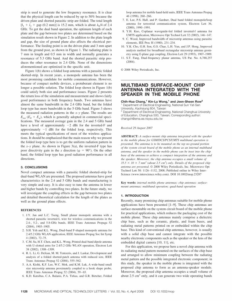
Figure 1(a) shows the geometry of the proposed chip antennaintegrated with the speaker for GSM/DCS/PCS/UMTS multibandoperation in the mobile phone. The antenna occupies an area of35.5 � 10 mm2 and is mounted on the top no-ground region at oneof the corners of the system circuit board of the mobile phone. A0.8-mm thick FR4 substrate of dimensions 40 � 90 mm2 is usedin the study to be considered as the system circuit board of themobile phone. The dimensions are reasonable for practical mobilephones. On the back side of the system circuit board, except on thetop no-ground region, there is a printed system ground plane.
There is also a 1-mm thick plastic housing (�r � 3.5, � � 0.02S/m) considered as the mobile phone housing enclosing the an-tenna and the system circuit board.
The antenna’s metal pattern is printed on the top, side, andbottom surfaces of the chip base as shown in Figure 1(b). Themetal pattern is composed of a longer radiating strip (strip 1 in thisstudy) on the top surface, a shorter radiating strip (strip 2) on thetop surface, a parasitic radiating strip (strip 3) on the bottomsurface, and a feeding strip on the side surface. Note that, for easyfabrication of the antenna in the experimental study, strips 1 and 2are printed on a 0.4-mm thick FR4 substrate of size 35.5 � 10mm2 and then attached onto the top surface of a foam base(relative permittivity close to that of air [1]). For strip 3, it isprinted on the top no-ground region of the system circuit board.The feeding strip of length 7 mm (AD) is cut from a copper strip,which is directly attached onto the side surface of the foam base.An area of 12.5 � 3 mm2 on the side surface of the foam base isthen cut with a depth of 8 mm to accommodate the speaker in themobile phone. For practical applications, a plastic chip base can beused and the antenna’s metal pattern can all be directly printed onthe surfaces of the plastic chip base.
Figure 1 (a) Geometry of the proposed multiband chip antenna inte-grated with the speaker in the mobile phone for GSM/DCS/PCS/UMTSmultiband operation. (b) Detailed dimensions of the antenna’s metal pat-tern on the top, side and bottom surfaces of the chip base. [Color figure canbe viewed in the online issue, which is available at www.interscience.wiley.com]
strips 1 and 2 printed on a 0.4-mm thick FR4 substrate (foam base removed for easy viewing)
(b)
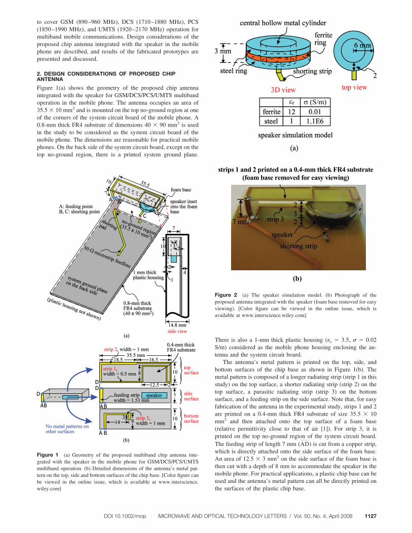
Figure 2 (a) The speaker simulation model. (b) Photograph of theproposed antenna integrated with the speaker (foam base removed for easyviewing). [Color figure can be viewed in the online issue, which isavailable at www.interscience.wiley.com]
DOI 10.1002/mop MICROWAVE AND OPTICAL TECHNOLOGY LETTERS / Vol. 50, No. 4, April 2008 1127
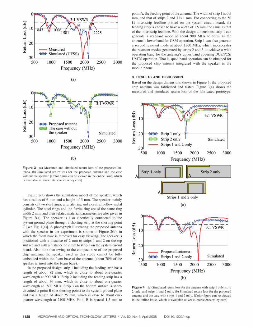
Figure 2(a) shows the simulation model of the speaker, whichhas a radius of 6 mm and a height of 3 mm. The speaker mainlyconsists of two steel rings, a ferrite ring and a central hollow metalcylinder. The steel rings and the ferrite ring are of the same ringwidth 2 mm, and their related material parameters are also given inFigure 2(a). The speaker is also electrically connected to thesystem ground plane through a shorting strip at the shorting pointC [see Fig. 1(a)]. A photograph illustrating the proposed antennawith the speaker in the experiment is shown in Figure 2(b), inwhich the foam base is removed for easy viewing. The speaker ispositioned with a distance of 2 mm to strips 1 and 2 on the topsurface and with a distance of 2 mm to strip 3 on the system circuitboard. Also note that owing to the compact size of the proposedchip antenna, the speaker used in this study cannot be fullyembedded within the foam base of the antenna (about 70% of thespeaker is inset into the foam base).
In the proposed design, strip 1 including the feeding strip has alength of about 82 mm, which is close to about one-quarterwavelength at 900 MHz. Strip 2 including the feeding strip has alength of about 36 mm, which is close to about one-quarterwavelength at 1800 MHz. Strip 3 on the bottom surface is short-circuited at point B (the shorting point) to the system ground planeand has a length of about 25 mm, which is close to about one-quarter wavelength at 2100 MHz. Point B is spaced 1.5 mm to
point A, the feeding point of the antenna. The width of strip 1 is 0.5mm, and that of strips 2 and 3 is 1 mm. For connecting to the 50� microstrip feedline printed on the system circuit board, thefeeding strip is chosen to have a width of 1.5 mm, the same as thatof the microstrip feedline. With the design dimensions, strip 1 cangenerate a resonant mode at about 900 MHz to form as theantenna’s lower band for GSM operation. Strip 1 can also generatea second resonant mode at about 1800 MHz, which incorporatesthe resonant modes generated by strips 2 and 3 to achieve a wideoperating band for the antenna’s upper band covering DCS/PCS/UMTS operation. That is, quad-band operation can be obtained forthe proposed chip antenna integrated with the speaker in themobile phone.
3. RESULTS AND DISCUSSION
Based on the design dimensions shown in Figure 1, the proposedchip antenna was fabricated and tested. Figure 3(a) shows themeasured and simulated return loss of the fabricated prototype.
Figure 3 (a) Measured and simulated return loss of the proposed an-tenna. (b) Simulated return loss for the proposed antenna and the casewithout the speaker. [Color figure can be viewed in the online issue, whichis available at www.interscience.wiley.com]
Figure 4 (a) Simulated return loss for the antenna with strip 1 only, strip2 only, and strips 1 and 2 only. (b) Simulated return loss for the proposedantenna and the case with strips 1 and 2 only. [Color figure can be viewedin the online issue, which is available at www.interscience.wiley.com]
1128 MICROWAVE AND OPTICAL TECHNOLOGY LETTERS / Vol. 50, No. 4, April 2008 DOI 10.1002/mop
The simulated results are obtained using Ansoft simulation soft-ware HFSS (High Frequency Structure Simulator) [12], and agree-ment between the measurement and simulation is seen. Two wideoperating bands of the antenna are excited. With 3:1 VSWR (6 dBreturn loss) definition, the measured bandwidth for the excitedlower band reaches 163 MHz (843–1006 MHz), while that of theupper band is as large as 644 MHz (1581–2225 MHz). The twooperating bands allow the antenna to cover GSM/DCS/PCS/UMTS multiband operation.
Effects of the integrated speaker on the performances of theantenna are studied, and results of the simulated return loss withand without the integrated speaker are shown in Figure 3(b). Somevariations in the simulated return loss are observed. However, theobtained bandwidths for both the lower and upper bands for thecase without the integrated speaker can still cover GSM/DCS/PCS/UMTS operation. This behavior is owing to the arrangement of thethree radiating strips (strips 1 to 3) to avoid direct crossing throughthe integrated speaker; in this case, minimum coupling between theantenna and the speaker can be obtained.
Dependence of the excited lower and upper bands on theantenna’s three radiating strips is studied in Figure 4. Results of thesimulated return loss for the case with strip 1 only, the case withstrip 2 only, and the case with strips 1 and 2 only are shown inFigure 4(a). Note that the corresponding dimensions of the threecases are the same as given in Figure 1. Results indicate that strip1 generates a fundamental or quarter-wavelength resonant mode atabout 900 MHz for GSM operation and a high-order or half-wavelength resonant mode at about 1750 MHz for DCS operation.Strip 2 generates a wide resonant mode (quarter-wavelength mode)at about 1800 MHz for PCS operation. For the case with strips 1and 2 only, the upper band formed by the two resonant modesprovided by strips 1 and 2 covers DCS/PCS operation, while thelower band controlled mainly by strip 1 still covers GSM opera-tion. By adding strip 3, an additional resonant mode at about 2100MHz is generated, which incorporates the two resonant modesprovided by strips 1 and 2 to form a much wider upper band tocover DCS/PCS/UMTS operation. This behavior is clearly seen inthe simulated return loss shown in Figure 4(b).
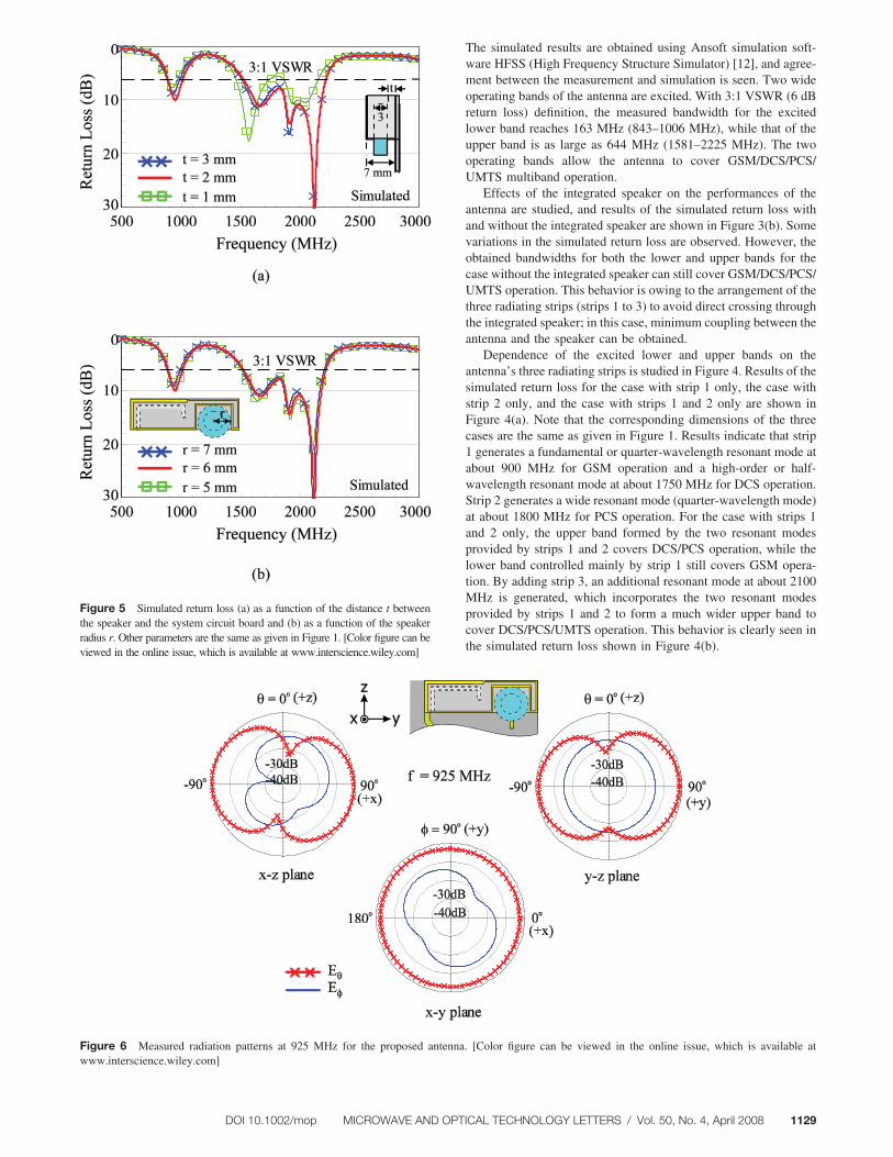
Figure 5 Simulated return loss (a) as a function of the distance t betweenthe speaker and the system circuit board and (b) as a function of the speakerradius r. Other parameters are the same as given in Figure 1. [Color figure can beviewed in the online issue, which is available at www.interscience.wiley.com]
Figure 6 Measured radiation patterns at 925 MHz for the proposed antenna. [Color figure can be viewed in the online issue, which is available atwww.interscience.wiley.com]
DOI 10.1002/mop MICROWAVE AND OPTICAL TECHNOLOGY LETTERS / Vol. 50, No. 4, April 2008 1129
Effects of the distance between the speaker and the systemcircuit board are studied in Figure 5(a). The distance is denoted tobe t as shown in the inset of the figure. Results of the simulatedreturn loss for the distance t varied from 1 to 3 mm are presented.It is seen that, except when t � 1 mm, the results are about thesame for t � 2 and 3 mm. This indicates that the speaker shouldbe placed at least 2-mm above the system circuit board to achievesmall variations in the antenna’s return loss. Figure 5(b) shows theeffects of the radius r of the speaker on the simulated return lossof the antenna. Three different cases with r � 5, 6, and 7 mm arestudied, and very small variations in the simulated return loss areseen. This suggests that, even for the case with a larger radius of
7 mm for the speaker, the proposed antenna with the integratedspeaker is capable of quad-band operation in the mobile phone.
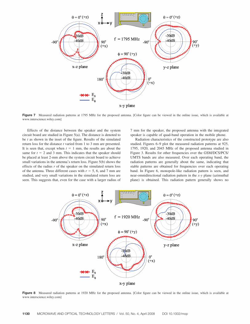
Radiation characteristics of the constructed prototype are alsostudied. Figures 6–9 plot the measured radiation patterns at 925,1795, 1920, and 2045 MHz of the proposed antenna studied inFigure 3. Results for other frequencies over the GSM/DCS/PCS/UMTS bands are also measured. Over each operating band, theradiation patterns are generally about the same, indicating thatstable patterns are obtained for frequencies over each operatingband. In Figure 6, monopole-like radiation pattern is seen, andnear-omnidirectional radiation pattern in the x-y plane (azimuthalplane) is obtained. This radiation pattern generally shows no
Figure 7 Measured radiation patterns at 1795 MHz for the proposed antenna. [Color figure can be viewed in the online issue, which is available atwww.interscience.wiley.com]
Figure 8 Measured radiation patterns at 1920 MHz for the proposed antenna. [Color figure can be viewed in the online issue, which is available atwww.interscience.wiley.com]
1130 MICROWAVE AND OPTICAL TECHNOLOGY LETTERS / Vol. 50, No. 4, April 2008 DOI 10.1002/mop
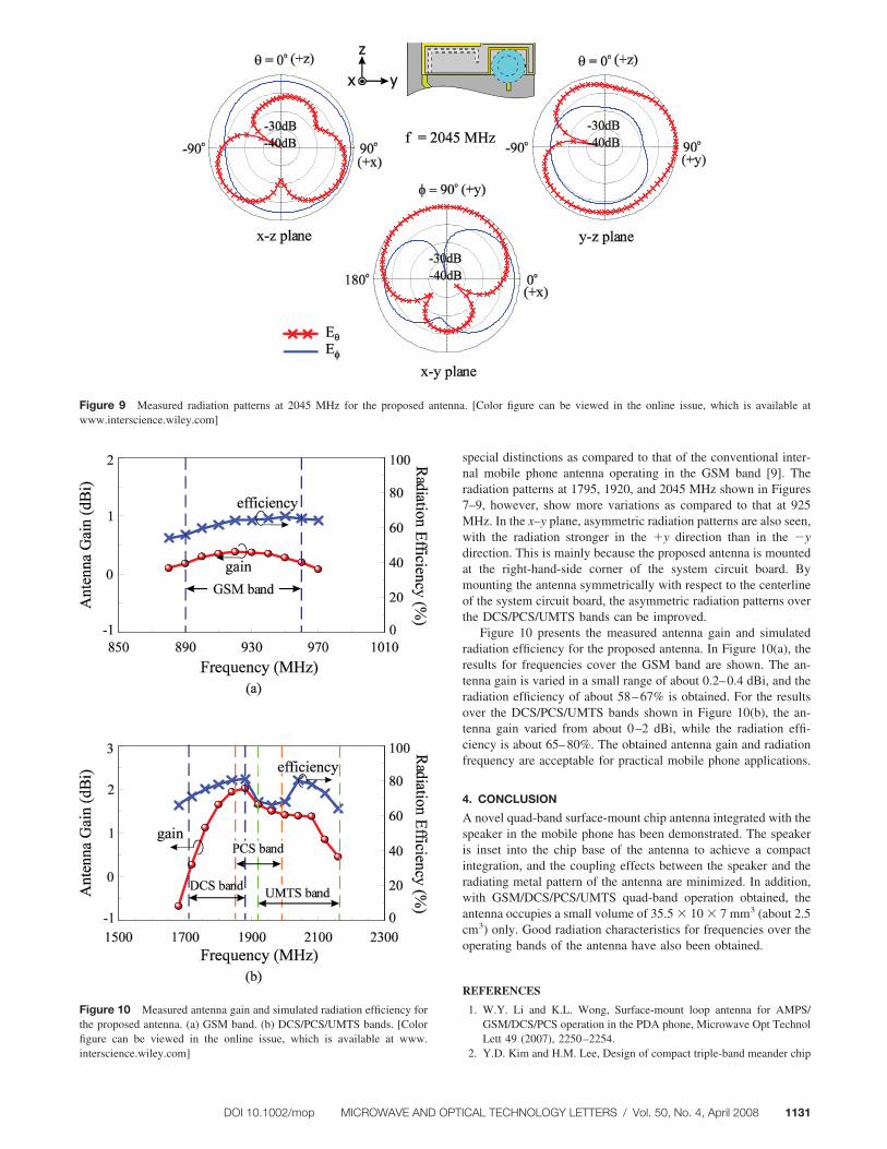
special distinctions as compared to that of the conventional inter-nal mobile phone antenna operating in the GSM band [9]. Theradiation patterns at 1795, 1920, and 2045 MHz shown in Figures7–9, however, show more variations as compared to that at 925MHz. In the x–y plane, asymmetric radiation patterns are also seen,with the radiation stronger in the �y direction than in the �ydirection. This is mainly because the proposed antenna is mountedat the right-hand-side corner of the system circuit board. Bymounting the antenna symmetrically with respect to the centerlineof the system circuit board, the asymmetric radiation patterns overthe DCS/PCS/UMTS bands can be improved.
Figure 10 presents the measured antenna gain and simulatedradiation efficiency for the proposed antenna. In Figure 10(a), theresults for frequencies cover the GSM band are shown. The an-tenna gain is varied in a small range of about 0.2–0.4 dBi, and theradiation efficiency of about 58–67% is obtained. For the resultsover the DCS/PCS/UMTS bands shown in Figure 10(b), the an-tenna gain varied from about 0–2 dBi, while the radiation effi-ciency is about 65–80%. The obtained antenna gain and radiationfrequency are acceptable for practical mobile phone applications.
4. CONCLUSION
A novel quad-band surface-mount chip antenna integrated with thespeaker in the mobile phone has been demonstrated. The speakeris inset into the chip base of the antenna to achieve a compactintegration, and the coupling effects between the speaker and theradiating metal pattern of the antenna are minimized. In addition,with GSM/DCS/PCS/UMTS quad-band operation obtained, theantenna occupies a small volume of 35.5 � 10 � 7 mm3 (about 2.5cm3) only. Good radiation characteristics for frequencies over theoperating bands of the antenna have also been obtained.
REFERENCES
1. W.Y. Li and K.L. Wong, Surface-mount loop antenna for AMPS/GSM/DCS/PCS operation in the PDA phone, Microwave Opt TechnolLett 49 (2007), 2250–2254.
2. Y.D. Kim and H.M. Lee, Design of compact triple-band meander chip
Figure 9 Measured radiation patterns at 2045 MHz for the proposed antenna. [Color figure can be viewed in the online issue, which is available atwww.interscience.wiley.com]
1.5 1.7 1.9 2.1 2.3
0.85 0.89 0.93 0.97 1.01
Figure 10 Measured antenna gain and simulated radiation efficiency forthe proposed antenna. (a) GSM band. (b) DCS/PCS/UMTS bands. [Colorfigure can be viewed in the online issue, which is available at www.interscience.wiley.com]
DOI 10.1002/mop MICROWAVE AND OPTICAL TECHNOLOGY LETTERS / Vol. 50, No. 4, April 2008 1131
antenna using LTCC technology for mobile handsets, Microwave OptTechnol Lett 48 (2006), 160–162.
3. Y.D. Kim, H.Y. Kim, and H.M. Lee, Dual-band LTCC chip antennadesign using stacked meander patch for mobile handsets, MicrowaveOpt Technol Lett 45 (2005), 271–273.
4. D.S. Yim, J. Kim, and S.O. Park, Novel wideband internal chipantenna for PCS/IMT-2000 dual-band applications, Microwave OptTechnol Lett 40 (2004), 324–326.
5. G.Y. Lee, H.T. Chen, and K.L. Wong, A low-cost surface-mountmonopole antenna for GSM/DCS operation, Microwave Opt TechnolLett 37 (2003), 2–4.
6. K.L. Wong, S.W. Su, T.W. Chiou, and Y.C. Lin, Dual-band plasticchip antenna for GSM/DCS mobile phones, Microwave Opt TechnolLett 33 (2002), 330–332.
7. S.H. Sim, C.Y. Kang, S.J. Yoon, Y.J. Yoon, and H.J. Kim, Broadbandmultilayer ceramic chip antenna for handsets, Electron Lett 38 (2002),205–207.
8. W. Choi, S. Kwon, and B. Lee, Ceramic chip antenna using meanderconductor lines, Electron Lett 37 (2001), 933–934.
9. K.L. Wong, Planar antennas for wireless communications, Wiley, NewYork, 2003.
10. C.M. Su, K.L. Wong, C.L. Tang, and S.H. Yeh, EMC internal patchantenna for UMTS operation in a mobile device, IEEE Trans AntennasPropagat 53 (2005), 3836–3839.
11. S.L. Chien, F.R. Hsiao, Y.C. Lin, and K.L. Wong, Planar inverted-Fantenna with a hollow shorting cylinder for mobile phone with anembedded camera, Microwave Opt Technol Lett 41 (2004), 418–419.
12. http://www.ansoft.com/products/hf/hfss/, Ansoft Corporation HFSS.
© 2008 Wiley Periodicals, Inc.
COMMENT ON “COMPACTMICROSTRIP BANDPASS FILTERUSING COMPOSITE RIGHT/LEFT-HANDED TRANSMISSION LINES”
Julien Perruisseau-CarrierCentre Tecnologic de Telecomunicacions de Catalunya (CTTC),Barcelona, Spain; Corresponding author: [email protected]
Received 8 November 2007
© 2008 Wiley Periodicals, Inc. Microwave Opt Technol Lett 50: 1132,2008; Published online in Wiley InterScience (www.interscience.wiley.com). DOI 10.1002/mop.23302
This comment concerns the general circuit modeling based on thetransmission (ABCD) and S-parameters matrices, in reference tothe work of Ref. 1.
In Ref. 1, the authors first write in (1) the ABCD matrix of a unitcell of the structure of interest, based on the circuit model for this cell.Then, they provide formulas (4) and (5), which are commonly used totransform ABCD matrix data into S-parameter ones, in the case of asymmetrical unit cell [2]. Equation (1) is then substituted into (4) and(5), which yield the S-parameters (6) and (7) as functions of the unitcell circuit elements and the reference impedance Z0.
The authors of Ref. 1 claim that (6) and (7) are valid for astructure of “infinite number of unit cells.” This is not true and (6)and (7) actually correspond to the S-parameter of a single unit cellconnected to reference impedances Z0. Indeed, the ABCD matrixof (1) itself represents a single unit cell, while the transformationfrom ABCD to S matrix employed subsequently [(4) and (5)]provides the S-parameters corresponding to the ABCD matrix usedfor the transformation, hence, here, a single unit cell [2].
In the case of an infinite number of cells, it is actually notpossible to define any S-parameters. However, note that the input
impedance of a semi-infinite structure could be calculated in thecase of a symmetrical unit cell as s11 � �ZB � Z0�/�ZB � Z0�,where Z0 is the reference impedance and ZB the Bloch waveequivalent impedance of the structure, defined as ZB � �B/C [2,3], where B and C are the element of the transmission matrix (1).
Finally, let us comment on the modeling of a finite structuremade of a cascade of N unit cells, which would be of use for thedesign of the device presented in Ref. 1. This case can bestudied by computing the ABCD matrix of the whole structure(this matrix is simply TN if T is the ABCD matrix of a unit cell)and applying (4) and (5) on TN rather than on T. However, it isin this case much more efficient to make use of the periodicBloch wave equivalents, as explained in detail in Ref. 3. Indeed,this approach allows analyzing a periodic structure with a finitenumber of unit cells in an exact way with regard to the circuitmodel of a cell [3], and thus provides a real modeling tool forcircuit-based design of finite periodic structure, which is not thecase of the formulas presented in Ref. 1.
REFERENCES
1. J. Li and Z. Yunyun, Compact microstrip bandpass filter using com-posite right/left-handed transmission lines, Microwave Opt TechnolLett 49 (2007), 1929–1931.
2. D.M. Pozar, Microwave engineering, Addison-Wesley, Reading, MA,1990.
3. J. Perruisseau-Carrier, R. Fritschi, P. Crespo-Valero, and A.K. Skriv-ervik, Modeling of periodic distributed MEMS, application to the de-sign of variable true-time delay lines, IEEE Trans Microwave TheoryTechnol, 54 (2006), 383–392.
© 2008 Wiley Periodicals, Inc.
ERRATUM: ELECTROMAGNETICPROPAGATION IN UNBOUNDEDINHOMOGENEOUS CHIRAL MEDIAUSING THE COUPLED MODE METHOD
Alvaro Gomez,1 Ismael Barba,1 Ana C. L. Cabeceira,1
Jose Represa,1 Angel Vegas,2 Ana Grande,2 andMiguel Angel Solano2
1 Departamento de Electricidad y Electronica, Universidad deValladolid, Paseo Prado de la Magdalena s/n. 47011 Valladolid,Spain; Corresponding author: [email protected] de Ingenierıa de Comunicaciones, Universidad deCantabria, Avenida de los Castros s/n. 39005 Santander, Spain
Received 5 September 2007
© 2008 Wiley Periodicals, Inc. Microwave Opt Technol Lett 50: 1132,2008; Published online in Wiley InterScience (www.interscience.wiley.com). DOI 10.1002/mop.23280
In our article [1], one author was missing. The correct list ofauthors and their affiliations appear above.
REFERENCES
1. A. Gomez, I. Barba, A.C.L. Cabeceira, J. Represa, A. Vegas, and M.A.Solano, Electromagnetic propagation in unbounded inhomogeneouschiral media using the coupled mode method, Microwave Opt TechnolLett 49 (2007), 2771-2779.
© 2008 Wiley Periodicals, Inc.
1132 MICROWAVE AND OPTICAL TECHNOLOGY LETTERS / Vol. 50, No. 4, April 2008 DOI 10.1002/mop