Embed Size (px)
Citation preview
1
Multi-Stage Transformation and Lattice Fluctuation
at AgCl-Ag Interface
Jingshan S. Du,†,‡,§,# Jungwon Park,*,†,⊥,○ QHwan Kim,∥ Wonho Jhe,∥ Vinayak P. Dravid,# Deren
Yang,*,‡ David A. Weitz†,¶
† School of Engineering and Applied Sciences, Harvard University, Cambridge, Massachusetts
02138, United States
‡ State Key Laboratory of Silicon Materials and School of Materials Science and Engineering,
Zhejiang University, Hangzhou 310027, People’s Republic of China
§ Chu Kochen Honors College, Zhejiang University, Hangzhou 310058, People’s Republic of
China
⊥ School of Chemical and Biological Engineering, Seoul National University, Gwanak-gu,
Seoul 151-747, Republic of Korea
○ Center for Nanoparticle Research, Institute for Basic Science (IBS), Seoul 08826, Republic of
Korea
# Department of Materials Science and Engineering, Northwestern University, Evanston, Illinois
60208, United States
∥ Department of Physics and Astronomy, Seoul National University, Gwanak-gu, Seoul 151-747,
Republic of Korea
¶ Department of Physics, Harvard University, Cambridge, Massachusetts 02138, United States
2
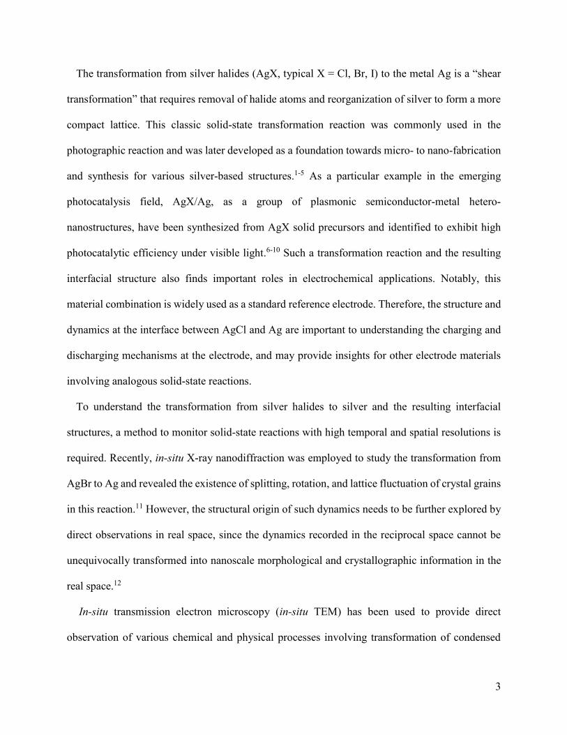
ABSTRACT Solid-state transformation is often accompanied by mechanical
expansion/compression, due to their volume change and structural evolution at interfaces at the
atomic scale. However, these two types of dynamics are usually difficult to monitor in the same
time. In this work, we use in-situ transmission electron microscopy to directly study the reduction
transformation at the AgCl-Ag interface. Three stages of lattice fluctuations were identified and
correlated to the structural evolution. During the steady state, a quasi-layered growth mode of Ag
in both vertical and lateral directions were observed due to the confinement of AgCl lattices. The
development of planar defects and depletion of AgCl are respectively associated with lattice
compression and relaxation. Topography and structure of decomposing AgCl was further
monitored by in-situ scanning transmission electron microscopy. Silver species are suggested to
originate from both the surface and the interior of AgCl, and be transported to the interface. Such
mass transport may have enabled the steady state and lattice compression in this volume-shrinking
transformation.
3
The transformation from silver halides (AgX, typical X = Cl, Br, I) to the metal Ag is a “shear
transformation” that requires removal of halide atoms and reorganization of silver to form a more
compact lattice. This classic solid-state transformation reaction was commonly used in the
photographic reaction and was later developed as a foundation towards micro- to nano-fabrication
and synthesis for various silver-based structures.1-5 As a particular example in the emerging
photocatalysis field, AgX/Ag, as a group of plasmonic semiconductor-metal hetero-
nanostructures, have been synthesized from AgX solid precursors and identified to exhibit high
photocatalytic efficiency under visible light.6-10 Such a transformation reaction and the resulting
interfacial structure also finds important roles in electrochemical applications. Notably, this
material combination is widely used as a standard reference electrode. Therefore, the structure and
dynamics at the interface between AgCl and Ag are important to understanding the charging and
discharging mechanisms at the electrode, and may provide insights for other electrode materials
involving analogous solid-state reactions.
To understand the transformation from silver halides to silver and the resulting interfacial
structures, a method to monitor solid-state reactions with high temporal and spatial resolutions is
required. Recently, in-situ X-ray nanodiffraction was employed to study the transformation from
AgBr to Ag and revealed the existence of splitting, rotation, and lattice fluctuation of crystal grains
in this reaction.11 However, the structural origin of such dynamics needs to be further explored by
direct observations in real space, since the dynamics recorded in the reciprocal space cannot be
unequivocally transformed into nanoscale morphological and crystallographic information in the
real space.12
In-situ transmission electron microscopy (in-situ TEM) has been used to provide direct
observation of various chemical and physical processes involving transformation of condensed
4
matters with multiple phases or components.13 This technology has further assisted the design and
optimization of many functional materials, such as Li-ion batteries,14-16 semiconductor nanowires
for electronics17-19 and functional nanoparticles.20-21 In particular, a TEM uses electrons as the
illumination source, which carry high energy and can induce the conversion from AgCl to Ag.
This property can enable direct observations of this reaction in high resolution using TEM.22-24
Mechanical behaviors of materials in nanoscale has also been extensively explored thanks to the
development of in-situ TEM nanomechanics with the aid of straining stages.25 The understanding
of plasticity and deformation mechanism in the atomic scale, for example, has been pushed
forward with such technologies.26-27 New data analysis methods such as strain mapping28-30 have
further enabled strain measurement directly from TEM images. With the emergence of these
technical advances for in-situ TEM, the dynamic mechanical behaviors of single crystalline grains
during a chemical reaction may be monitored in real time.
Here, we report the multi-stage transformation processes from AgCl to Ag and the lattice
fluctuation with atomic-scale resolution at their interface, directly observed by in-situ TEM. The
electron beam (e-beam) in TEM serves a second function in addition to imaging: high energy
electrons irradiating AgCl can induce its reductive conversion to Ag and the resulting removal of
Cl from the lattice. 11, 24 We monitored the growth of Ag along the AgCl-Ag atomic interface when
the AgCl lattice is stable. Lattice compression and relaxation are shown to be associated with
defect formation and AgCl depletion, respectively.
The AgCl-Ag heterojunction sample for in-situ TEM was prepared by mixing AgNO3 and KCl
solutions, centrifugation, and subsequent drop-casting on a TEM grid. Detailed procedures are
described in the Methods Section in the Supporting Information. Light-induced reductive
conversion under ambient conditions and the initial e-beam exposure during sample searching
5
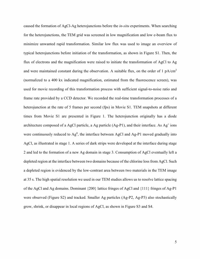
caused the formation of AgCl-Ag heterojunctions before the in-situ experiments. When searching
for the heterojunctions, the TEM grid was screened in low magnification and low e-beam flux to
minimize unwanted rapid transformation. Similar low flux was used to image an overview of
typical heterojunctions before initiation of the transformation, as shown in Figure S1. Then, the
flux of electrons and the magnification were raised to initiate the transformation of AgCl to Ag
and were maintained constant during the observation. A suitable flux, on the order of 1 pA/cm2
(normalized to a 400 kx indicated magnification, estimated from the fluorescence screen), was
used for movie recording of this transformation process with sufficient signal-to-noise ratio and
frame rate provided by a CCD detector. We recorded the real-time transformation processes of a
heterojunction at the rate of 5 frames per second (fps) in Movie S1. TEM snapshots at different
times from Movie S1 are presented in Figure 1. The heterojunction originally has a diode
architecture composed of a AgCl particle, a Ag particle (Ag-P1), and their interface. As Ag+ ions
were continuously reduced to Ag0, the interface between AgCl and Ag-P1 moved gradually into
AgCl, as illustrated in stage 1. A series of dark strips were developed at the interface during stage
2 and led to the formation of a new Ag domain in stage 3. Consumption of AgCl eventually left a
depleted region at the interface between two domains because of the chlorine loss from AgCl. Such
a depleted region is evidenced by the low-contrast area between two materials in the TEM image
at 35 s. The high spatial resolution we used in our TEM studies allows us to resolve lattice spacing
of the AgCl and Ag domains. Dominant {200} lattice fringes of AgCl and {111} fringes of Ag-P1
were observed (Figure S2) and tracked. Smaller Ag particles (Ag-P2, Ag-P3) also stochastically
grow, shrink, or disappear in local regions of AgCl, as shown in Figure S3 and S4.
6
Figure 1. Time-series TEM images showing the transformation progress of a heterojunction and
associated schematic illustrations. The initial heterojunction consists of an AgCl and an Ag (Ag-
P1) part. Newly nucleated Ag Particle 2 and 3 (Ag-P2, Ag-P3) are marked at 10 s and 20 s,
respectively. Scale bars are 10 nm. Ag (red) and AgCl (blue) parts are shown in the illustrations.
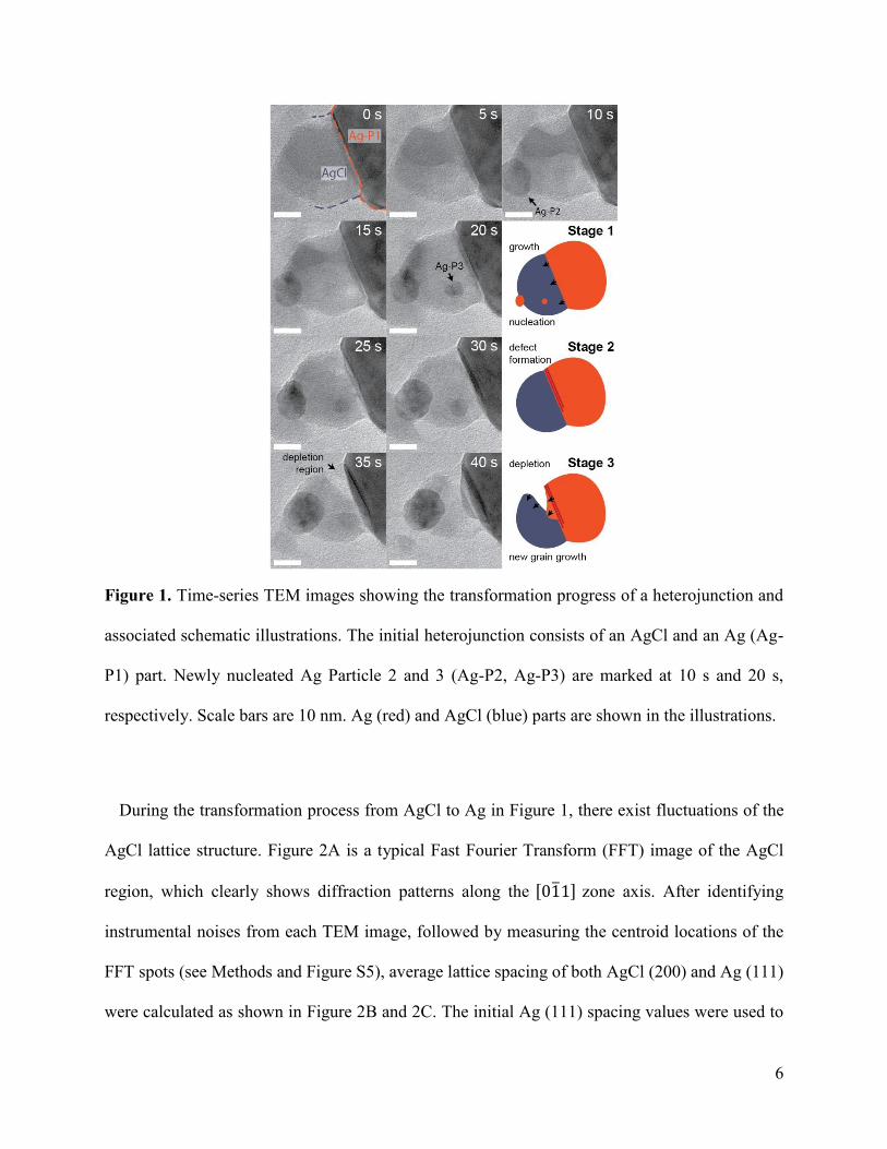
During the transformation process from AgCl to Ag in Figure 1, there exist fluctuations of the
AgCl lattice structure. Figure 2A is a typical Fast Fourier Transform (FFT) image of the AgCl
region, which clearly shows diffraction patterns along the [01̅1] zone axis. After identifying
instrumental noises from each TEM image, followed by measuring the centroid locations of the
FFT spots (see Methods and Figure S5), average lattice spacing of both AgCl (200) and Ag (111)
were calculated as shown in Figure 2B and 2C. The initial Ag (111) spacing values were used to
7
calibrate the image scale with respect to standard lattice parameters. In this case, the average lattice
spacing is mathematically defined as the weighted mean value of spatial frequencies in the
reciprocal space. While the reference lattice of Ag (111) remains stable with only sub-2%
fluctuations throughout the transformation, the AgCl (200) lattice spacing shows three different
stages according to Figure 2C. In stage 1, the lattice spacing was generally steady around the
standard value of 0.277 nm with fluctuations of ca. ±0.5%. It was continuously compressed to
about 0.271 nm in stage 2, and then increased to pass beyond the standard value in stage 3. The
orientation of the AgCl lattice also changed accordingly in these stages as shown in Figure S6.
Figure 2. Lattice structure fluctuation during the transformation. (A) Typical FFT patterns from
the AgCl region along the [01̅1] zone axis. (B) Temporal fluctuation of AgCl (200) spot from the
blue box in (A). Yellow dashed lines are shown for the centroid position at 8 s. Blue circles
indicates the centroid position of the spots in each image. (C) Average AgCl (200) (blue) and Ag-
P1 (111) (orange) lattice spacing as a function of time shows three distinct stages. Standard AgCl
(200) and Ag (111) lattice spacing values are shown in dashed lines for reference.
8
The steady state—compression—relaxation three-stage process of the lattice fluctuation well
accommodates the temporal regimes of three stages distinguished by the morphological evolution
(Figure 1). To understand the underlying mechanisms, we correlated the structural changes of the
AgCl-Ag interface and the lattice fluctuations in each stage.
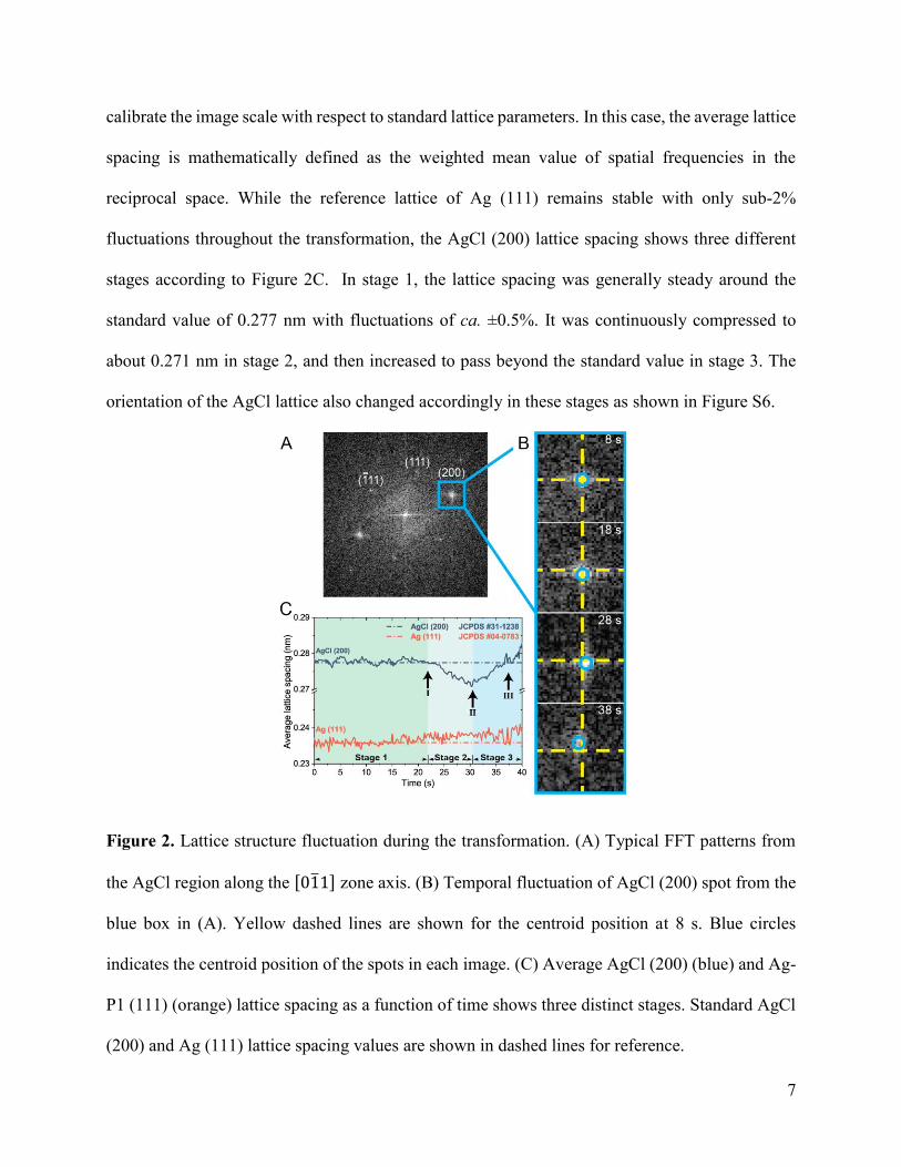
Mechanically steady-state solid transformation occurs in stage 1. During this time, multiple
monolayers of Ag were grown on the flat interface between AgCl and Ag. This interface, indicated
by a black line in the color-enhanced TEM image (Figure 3A), is well aligned with the (200) lattice
of AgCl. The Ag layers were continuously generated and extended along the interface, which is
evidenced by the movement of their edges (black arrows) at different time. In addition, the growth
pattern of silver was investigated by analyzing the contrasts in magnified TEM snapshots with
corresponding schematic illustrations in Figure 3B, noting that the metallic Ag region shows
significantly darker contrast than the AgCl region. With continuous reduction of Ag+ from AgCl,
at the initial stage (a), several segments and islands of Ag are formed at the interface of AgCl and
Ag. Segmented lines in the TEM snapshot (2.0 s) indicate the forefronts of three discontinuous Ag
segments, while the position of original interface is also marked for reference. As further
attachment of monomers proceeds, these segments and islands connect laterally, as shown in stage
(b). More islands are formed in front of the edge (2.6 s). These multiple monolayers of Ag continue
to grow laterally and connect with new islands until the entire interface is filled in stage (c), also
shown by the TEM image at 3.0 s. After being completely filled, the interface typically remains
stable for a few seconds before new layers start to form following similar processes. It is worth
pointing out that the growth does not follow exact layer-by-layer processes of monolayer
attachment. Instead, the vertical height of the forming Ag layers also increases during their lateral
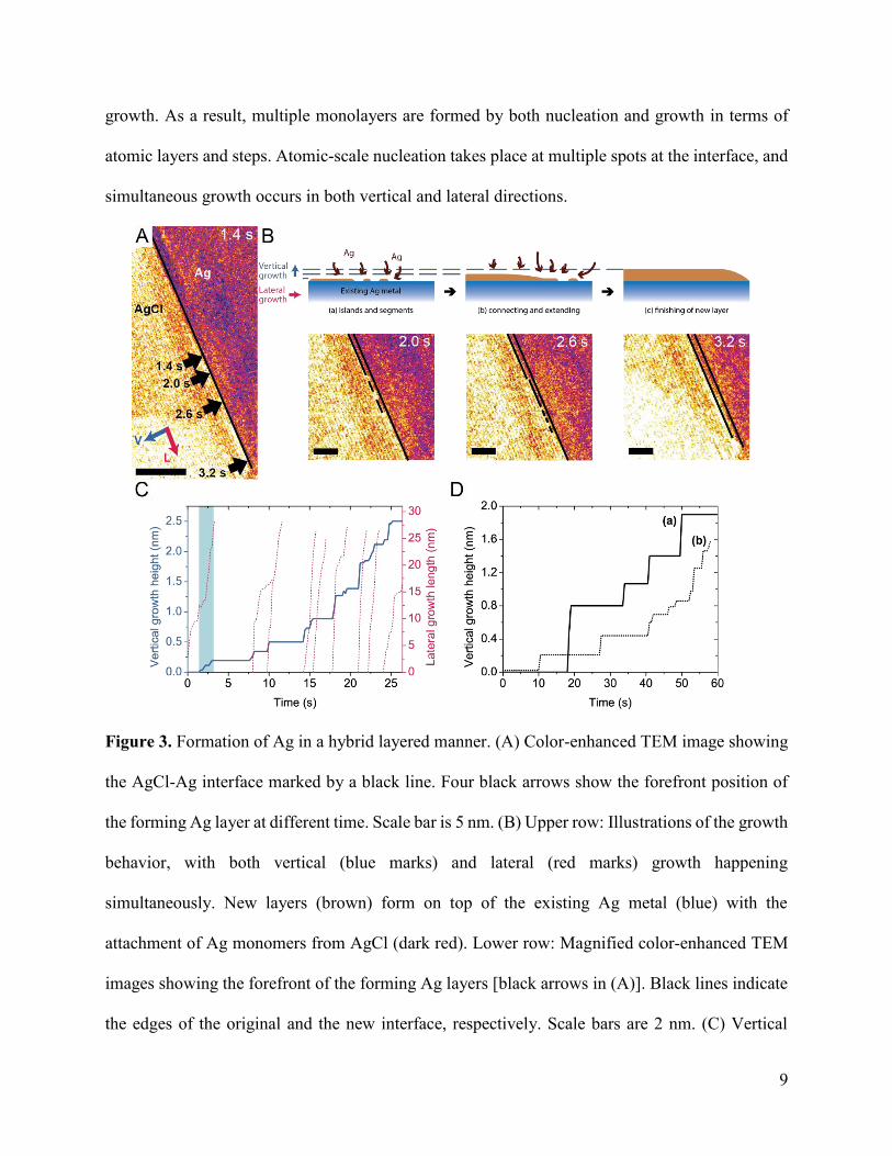
9
growth. As a result, multiple monolayers are formed by both nucleation and growth in terms of
atomic layers and steps. Atomic-scale nucleation takes place at multiple spots at the interface, and
simultaneous growth occurs in both vertical and lateral directions.
Figure 3. Formation of Ag in a hybrid layered manner. (A) Color-enhanced TEM image showing
the AgCl-Ag interface marked by a black line. Four black arrows show the forefront position of
the forming Ag layer at different time. Scale bar is 5 nm. (B) Upper row: Illustrations of the growth
behavior, with both vertical (blue marks) and lateral (red marks) growth happening
simultaneously. New layers (brown) form on top of the existing Ag metal (blue) with the
attachment of Ag monomers from AgCl (dark red). Lower row: Magnified color-enhanced TEM
images showing the forefront of the forming Ag layers [black arrows in (A)]. Black lines indicate
the edges of the original and the new interface, respectively. Scale bars are 2 nm. (C) Vertical
10
height of the forefront (blue) and the lateral length of each layer (right, red). A blue shading
indicates the time span of images in (A). (D) Vertical height of another two heterojunctions in
Movie S2 (a) and Movie S3 (b) also shows stepped behaviors.
The kinetics of vertical and lateral growth is demonstrated by measuring the vertical height of
the interface forefront (blue) and the lateral length of each forming layer (red) in Figure 3C. The
blue curve shows stepped growth of the Ag layers in the vertical direction with respect to the
interface, which resulted from the sequential formation of multiple monolayers. According to this
measurement, the lateral growth rate of layers is almost two orders higher than the overall vertical
growth rate. Simultaneous growth in both directions is shown by the shaded region, which
corresponds to the growth events in Figure 3A. While the lateral growth progresses, the vertical
height of the forefront interface rises gradually from zero to 0.19 nm in ca. 1.8 s, rather than
jumping to the final height suddenly. Interestingly, multiple lateral growth sometimes takes place
concurrently. For example, two red curves coexist from around 10 s. The growth of a second layer
commenced before the completion of the first one, and eventually, these two growing layers
merged into one thicker layer at 10.6 s and proceeded to fill the remaining space.
We found that the similar transformation pattern occurs at interfaces aligned with different
crystallographic orientations of AgCl domains. The two curves (a) and (b) in Figure 3D are the
vertical heights at the interfaces aligned with AgCl (111) and (200) in the two heterojunctions
shown in Figure S7, respectively. Corresponding in-situ TEM movies are supplied in Movie S2
and S3. These two curves indicate that the vertical growth in different heterojunctions is stepped
with uneven step sizes. Though both exhibit a discontinuity, such a growth pattern of the new
phase is different from the layered or stepped growth mode recently reported in vapor phase growth
11
of nanowires31-32 and solid replacement of semiconductors,17, 33 where vertical growth is
accomplished by sequential growth of monolayers. In those cases, the low monomer concentration
guarantees that monomer attachment preferentially takes place at atomic steps. Differently, our
observations presumably demonstrate the interfacial growth in a supersaturated environment with
lattice confinements. In our case, simultaneous growth of Ag to both vertical and lateral directions
along the AgCl lattice is likely induced by a faster generation of Ag0 than the depletion rate due to
diffusion, in which supersaturated Ag monomers can initiate the formation of multiple nuclei at
the interface in addition to the growth on atomic steps. Moreover, the growth of Ag is constrained
by the charged framework of AgCl lattices, which leads to a layered growth behavior. This
hypothesis is also evidenced by the nucleation and fast growth of Ag-P2 and Ag-P3 at around 8 s
and 18 s, as shown in the TEM images in Figure 1 and the corresponding size evolution in Figure
S4. Such homogeneous nucleation within the AgCl domain usually requires even higher
supersaturation of monomers than heterogeneous nucleation (or growth) at an existing interface.34-
36 We emphasize that the decomposition behavior of AgCl may be dependent on the parameters of
the irradiation. For instance, a higher flux and energy causes noticable sub-second fluctuations of
the contrast in Ag and AgCl domains, indicating strong diffusion inside the crystals (Figure S8).
In stage 2 and 3, the (200) lattice of AgCl underwent a dynamical fluctuation. In stage 2, the
AgCl lattice was continuously compressed when the Ag domain further grew, as shown in Figure
2C. As the compression continued from ca. 22 s (point I) to ca. 30 s (point II), a series of planar
defects on Ag formed near its interface with AgCl. Color-enhanced TEM images show the
formation of these planar defects in Figure 4A by observing the associated dark strips. Two dark
strips successively formed near the upper region of the interface at 24 s and 26 s, as indicated by
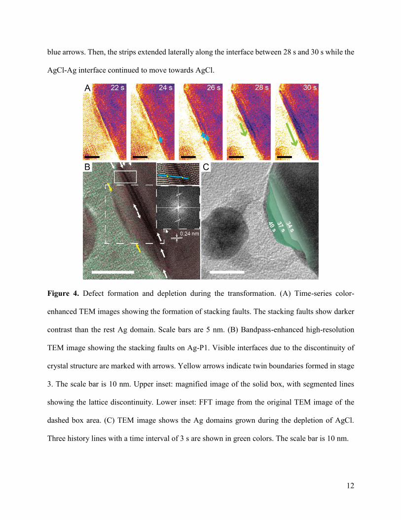
12
blue arrows. Then, the strips extended laterally along the interface between 28 s and 30 s while the
AgCl-Ag interface continued to move towards AgCl.
Figure 4. Defect formation and depletion during the transformation. (A) Time-series color-
enhanced TEM images showing the formation of stacking faults. The stacking faults show darker
contrast than the rest Ag domain. Scale bars are 5 nm. (B) Bandpass-enhanced high-resolution
TEM image showing the stacking faults on Ag-P1. Visible interfaces due to the discontinuity of
crystal structure are marked with arrows. Yellow arrows indicate twin boundaries formed in stage
3. The scale bar is 10 nm. Upper inset: magnified image of the solid box, with segmented lines
showing the lattice discontinuity. Lower inset: FFT image from the original TEM image of the
dashed box area. (C) TEM image shows the Ag domains grown during the depletion of AgCl.
Three history lines with a time interval of 3 s are shown in green colors. The scale bar is 10 nm.
13
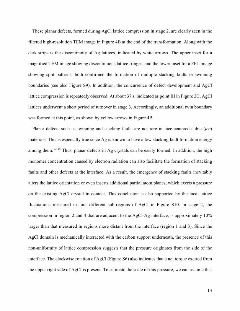
These planar defects, formed during AgCl lattice compression in stage 2, are clearly seen in the
filtered high-resolution TEM image in Figure 4B at the end of the transformation. Along with the
dark strips is the discontinuity of Ag lattices, indicated by white arrows. The upper inset for a
magnified TEM image showing discontinuous lattice fringes, and the lower inset for a FFT image
showing split patterns, both confirmed the formation of multiple stacking faults or twinning
boundaries (see also Figure S9). In addition, the concurrence of defect development and AgCl
lattice compression is repeatedly observed. At about 37 s, indicated as point III in Figure 2C, AgCl
lattices underwent a short period of turnover in stage 3. Accordingly, an additional twin boundary
was formed at this point, as shown by yellow arrows in Figure 4B.
Planar defects such as twinning and stacking faults are not rare in face-centered cubic (fcc)
materials. This is especially true since Ag is known to have a low stacking fault formation energy
among them.37-38 Thus, planar defects in Ag crystals can be easily formed. In addition, the high
monomer concentration caused by electron radiation can also facilitate the formation of stacking
faults and other defects at the interface. As a result, the emergence of stacking faults inevitably
alters the lattice orientation or even inserts additional partial atom planes, which exerts a pressure
on the existing AgCl crystal in contact. This conclusion is also supported by the local lattice
fluctuations measured in four different sub-regions of AgCl in Figure S10. In stage 2, the
compression in region 2 and 4 that are adjacent to the AgCl-Ag interface, is approximately 10%
larger than that measured in regions more distant from the interface (region 1 and 3). Since the
AgCl domain is mechanically interacted with the carbon support underneath, the presence of this
non-uniformity of lattice compression suggests that the pressure originates from the side of the
interface. The clockwise rotation of AgCl (Figure S6) also indicates that a net torque exerted from
the upper right side of AgCl is present. To estimate the scale of this pressure, we can assume that
14
the AgCl nanocrystal shares the same linear elastic constants with bulk single crystals at room
temperature.39 By neglecting the strains in other directions, we calculated the stress corresponding
to a normal strain of ca. -2.4% (with respect to the AgCl-Ag interface) to be 𝜎11 ≈ 𝐶11𝜖11 ≈
−1.44 GPa. In comparison, compression of AgCl bulk crystals at 𝑉/𝑉0 = 0.97 yielded a similar
pressure of 1.5 GPa.40 These results suggest that the mechanical behavior of the single AgCl
nanocrystal in our observation is in a reasonable range.
In stage 3, the compressed AgCl lattice was relaxed, as shown in Figure 2C. This change is due
to the depletion of AgCl at the interface between the two materials, as shown in the TEM images
in the last row of Figure 1. Consequently, the AgCl domain detached from the Ag domain, thus
the (200) lattice of AgCl was gradually relieved from compression. In the same period, continuous
growth of a new Ag domain was observed. Three history lines that show the surface of the growing
Ag domain at different time are illustrated in Figure 4C. Contrary to the growth mode in stage 1,
in which the front boundary of growing Ag formed a stepped, flat interface, a curved boundary of
the Ag domain was observed in stage 3. Our previous discussions have shown that the interface
morphology between AgCl and Ag in stage 1 is likely limited by the rigid and charged framework
of chlorine ions,41-42 which need to be sequentially removed during the AgCl-to-Ag
transformation. In stage 3, however, Ag growth towards the depleted space is no longer subject to
such a confinement. Therefore, the newly formed domain achieves the minimum surface energy
by having a quasi-spherical morphology.
When AgCl is transformed to Ag, the volume of the whole heterojunction decreases due to the
mass loss of Cl. If the reduction only involves atoms at the interface, then the receding rate of the
AgCl boundary should be higher than the growth rate of Ag. Consequently, a tensile strain should
be expected, similar to what is observed after about 37 s (Figure 2C), and depletion would form at
15
the very beginning of the transformation. So how is it possible that the interface can move into
AgCl steadily and a lattice compression can exist? In the previous discussions, we implicitly
hypothesized that the reduced silver atoms can originate from other locations in the AgCl crystal
and then diffuse to the interface. This hypothesis means that the formation rate of Ag at the
interface is not necessarily lower than the receding rate of AgCl during the first two stages of our
observation.
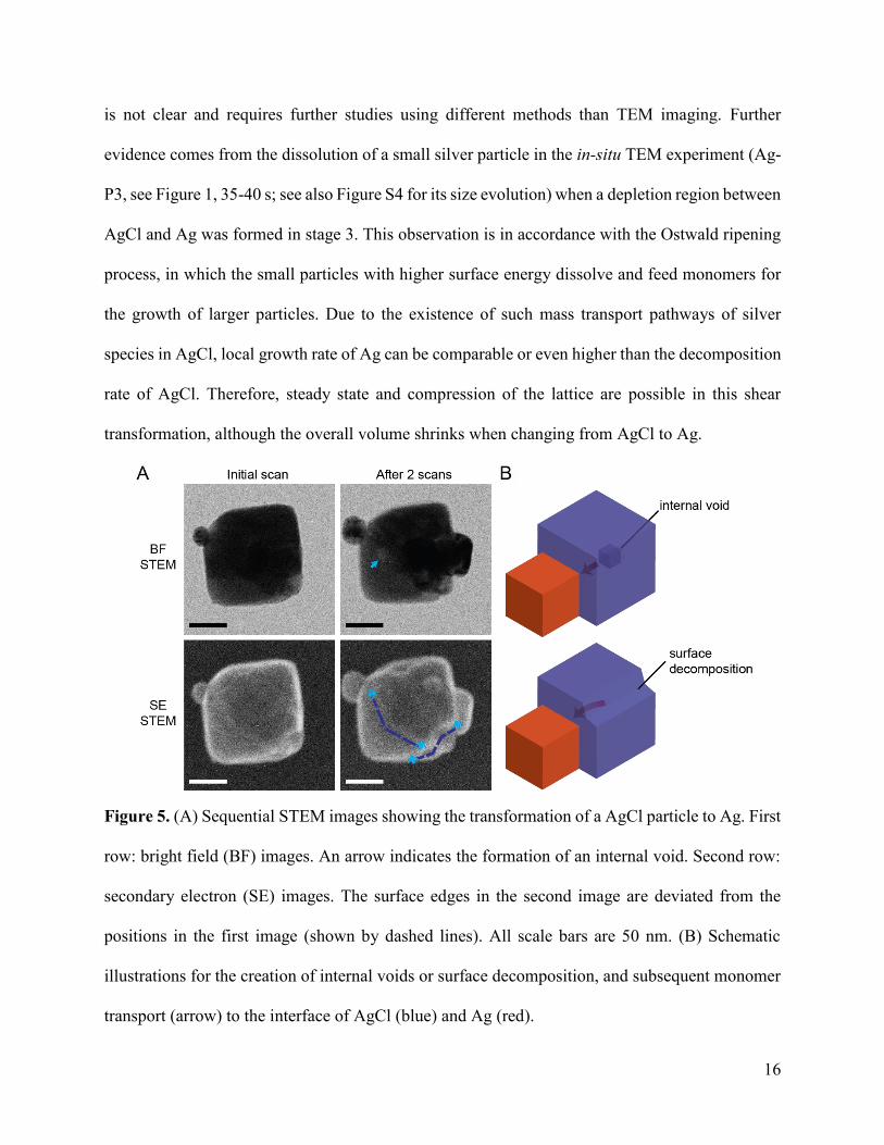
To better evaluate this hypothesized mechanism, we used in-situ scanning transmission electron
microscopy (STEM) with simultaneous secondary electron (SE) and bright field (BF) signals to
investigate the topography and structure of transforming AgCl crystals at the same time. We
observed that the decomposition of AgCl can happen in two ways, as indicated by the sequential
microscopy images and corresponding schematic illustrations in Figure 5. For decomposition
inside the crystal, formation of a low-density region (e.g., shown by the blue arrow) in the BF
image without observable changes in the SE images indicates the formation of internal voids.
Decomposition at the surface of AgCl is demonstrated by the recessing steps in the SE images, as
the surface edges in the second image are deviated from their positions in the first image (shown
by the dashed lines). Both two pathways can be potentially matched with phenomena in the in-situ
TEM observations (Figure 1): interior decomposition may be correlated with the formation of a
bright region at 10-15 s, and surface decomposition may be correlated with the diminishing of a
dark region during 0-20 s. Importantly, both two observed pathways have decomposition locations
away from the Ag-AgCl interfaces. These results suggest that the Ag atoms that attach to the Ag
particle at the interface originate from both the interior and the surface of AgCl, and then transport
to the AgCl-Ag interface, possibly due to the high Ag cation mobility in AgCl.41-42 Note that how
the chlorine ions disassemble and diffuse, and how the charge distribution on the particles evolve
16
is not clear and requires further studies using different methods than TEM imaging. Further
evidence comes from the dissolution of a small silver particle in the in-situ TEM experiment (Ag-
P3, see Figure 1, 35-40 s; see also Figure S4 for its size evolution) when a depletion region between
AgCl and Ag was formed in stage 3. This observation is in accordance with the Ostwald ripening
process, in which the small particles with higher surface energy dissolve and feed monomers for
the growth of larger particles. Due to the existence of such mass transport pathways of silver
species in AgCl, local growth rate of Ag can be comparable or even higher than the decomposition
rate of AgCl. Therefore, steady state and compression of the lattice are possible in this shear
transformation, although the overall volume shrinks when changing from AgCl to Ag.
Figure 5. (A) Sequential STEM images showing the transformation of a AgCl particle to Ag. First
row: bright field (BF) images. An arrow indicates the formation of an internal void. Second row:
secondary electron (SE) images. The surface edges in the second image are deviated from the
positions in the first image (shown by dashed lines). All scale bars are 50 nm. (B) Schematic
illustrations for the creation of internal voids or surface decomposition, and subsequent monomer
transport (arrow) to the interface of AgCl (blue) and Ag (red).
17
To further evaluate other possible factors that can induce lattice fluctuations, we analyzed the
dynamic ranges of thermal shrinkage and grain rotation, and potential errors in the measurement.
Figure S11A shows the thermal expansion and shrinkage data of fcc AgCl crystals, extracted from
a previous X-ray diffraction (XRD) study.43 In comparison, the dynamic range from our
observations is far lower than thermal shrinkage can reach, even down to -190 °C. As for grain
rotation, since a TEM image is a 2D projection, tilted crystal zone axis will lead to a multiplicity
of cos 𝜃 to the observed lattice spacing in small angles. However, this effect is very small
compared to the dynamic range of our experiment. As can be seen in Figure S11B and C, the
allowed crystal tilt angle is only within a few degrees to enable clear observation of lattice fringes
from coherent TEM image simulation.44 Such small tolerance angle is confirmed by analyzing the
fringe-visibility band.45 In addition, the potential measurement errors of lattice fringes are also
significantly less than the dynamic range of compression–relaxation observed in this work.
Detailed simulation procedures, parameters and discussions are given in the Supporting
Information (Text S2–S4). Thus, the observed lattice fluctuation can be attributed predominantly
to crystal compression which is associated with structural changes, rather than the two external
factors.
In summary, a multi-stage transformation process from AgCl to Ag at their interfaces has been
observed by in-situ high resolution TEM. We showed a steady state—compression—relaxation
three-stage process of the lattice structure of AgCl, correlated with different structural evolution
during the transformation. The presence of AgCl lattices directed formation of a flat and stepped
interface as well as a quasi-layered growth mode in the steady state. Mass transport of Ag
18
monomers across the AgCl crystal, either from the interior or the surface, to the AgCl-Ag interface
enabled highly supersaturated growth behaviors and development of planar defects. We further
showed that defect formation is associated with the compression of AgCl lattice, and the resulted
strain is then relaxed due to the depletion of AgCl at the end of the transformation. Importantly,
the steady state and lattice compression observed in this work will not be possible without the
existence of mass transport in the converting crystal domain. We argue that in general solid-state
transformations, such mass transport must be taken into consideration when judging the type of
mechanical behaviors that may exist. Therefore, the results of this in-situ observation not only
provides important details in the reduction conversion of silver halides, but can also shine light on
other materials systems with similar volume change during the conversion.
ASSOCIATED CONTENT
Supporting Information. Methods, additional data analysis and simulation details (Figures S1-
S11), and three real-time lattice-resolution TEM movies (Movies S1-S3). This material is
available free of charge via the Internet at http://pubs.acs.org.
AUTHOR INFORMATION
Corresponding Author
*Email: [email protected] (J.P.), [email protected] (D.Y.)
Notes
The authors declare no competing financial interests.
ACKNOWLEDGMENT
19
We would like to thank Prof. Frans Spaepen (Harvard University), Prof. Jianwei Miao
(University of California, Los Angeles) and Mr. Yi Yang (National Astronomical Observatory of
Japan) for helpful discussions. This work was performed in part at the Center for Nanoscale
Systems (CNS) at Harvard University, supported under NSF award no. ECS-0335765; the EPIC
facility of the NUANCE Center at Northwestern University, supported by the SHyNE Resource
(NSF NNCI-1542205), the MRSEC program (NSF DMR-1121262), the International Institute
for Nanotechnology (IIN), the Keck Foundation, and the State of Illinois through the IIN. The
work at Harvard was supported by the Harvard MRSEC (DMR- 1420570) and the NSF (DMR-
1310266). J. P acknowledge support by IBS-R006-D1. J.S.D. acknowledges support from
Zhejiang University Chu Kochen Honors College.
REFERENCES
(1) Wiley, B.; Sun, Y.; Xia, Y. Synthesis of Silver Nanostructures with Controlled Shapes and
Properties. Acc. Chem. Res. 2007, 40, 1067-1076.
(2) Ballantyne, J. P.; Nixon, W. C. Selective Area Metallization by Electron-Beam Controlled
Direct Metallic Deposition. J. Vac. Sci. Technol. 1973, 10, 1094-1097.
(3) Kolwicz, K. D.; Chang, M. S. Silver Halide‐Chalcogenide Glass Inorganic Resists for X‐Ray Lithography. J. Electrochem. Soc. 1980, 127, 135-138.
(4) Deng, T.; Arias, F.; Ismagilov, R. F.; Kenis, P. J. A.; Whitesides, G. M. Fabrication of Metallic
Microstructures Using Exposed, Developed Silver Halide-Based Photographic Film. Anal. Chem.
2000, 72, 645-651.
(5) Schuette, W. M.; Buhro, W. E. Silver Chloride as a Heterogeneous Nucleant for the Growth of
Silver Nanowires. ACS Nano 2013, 7, 3844-3853.
(6) Wang, P.; Huang, B.; Qin, X.; Zhang, X.; Dai, Y.; Wei, J.; Whangbo, M.-H. Ag@AgCl: A
Highly Efficient and Stable Photocatalyst Active under Visible Light. Angew. Chem. Int. Ed. 2008,
47, 7931-7933.
(7) An, C.; Peng, S.; Sun, Y. Facile Synthesis of Sunlight-Driven AgCl:Ag Plasmonic
Nanophotocatalyst. Adv. Mater. 2010, 22, 2570-2574.
(8) An, C.; Wang, R.; Wang, S.; Zhang, X., Converting AgCl Nanocubes to Sunlight-Driven
Plasmonic AgCl : Ag Nanophotocatalyst with High Activity and Durability. J. Mater. Chem. 2011,
21, 11532-11536.
(9) An, C.; Wang, J.; Jiang, W.; Zhang, M.; Ming, X.; Wang, S.; Zhang, Q. Strongly Visible-light
Responsive Plasmonic Shaped AgX:Ag (X = Cl, Br) Nanoparticles for Reduction of CO2 to
Methanol. Nanoscale 2012, 4, 5646-5650.
20
(10) Tang, Y.; Jiang, Z.; Xing, G.; Li, A.; Kanhere, P. D.; Zhang, Y.; Sum, T. C.; Li, S.; Chen, X.;
Dong, Z.; Chen, Z. Efficient Ag@AgCl Cubic Cage Photocatalysts Profit from Ultrafast Plasmon-
Induced Electron Transfer Processes. Adv. Funct. Mater. 2013, 23, 2932-2940.
(11) Huang, Z.; Bartels, M.; Xu, R.; Osterhoff, M.; Kalbfleisch, S.; Sprung, M.; Suzuki, A.;
Takahashi, Y.; Blanton, T. N.; Salditt, T.; Miao, J. Grain Rotation and Lattice Deformation during
Photoinduced Chemical Reactions Revealed by in situ X-ray Nanodiffraction. Nat. Mater. 2015,
14, 691-695.
(12) Sturmat, M.; Koch, R.; Rieder, K. H. Real Space Investigation of the Roughening and
Deconstruction Transitions of Au(110). Phys. Rev. Lett. 1996, 77, 5071-5074.
(13) Campbell, G. H.; McKeown, J. T.; Santala, M. K. Time Resolved Electron Microscopy for in
situ Experiments. Appl. Phys. Rev. 2014, 1, 041101.
(14) Huang, J. Y.; Zhong, L.; Wang, C. M.; Sullivan, J. P.; Xu, W.; Zhang, L. Q.; Mao, S. X.;
Hudak, N. S.; Liu, X. H.; Subramanian, A.; et al. In Situ Observation of the Electrochemical
Lithiation of a Single SnO2 Nanowire Electrode. Science 2010, 330, 1515-1520.
(15) Liu, X. H.; Wang, J. W.; Huang, S.; Fan, F.; Huang, X.; Liu, Y.; Krylyuk, S.; Yoo, J.; Dayeh,
S. A.; Davydov, A. V.; et al. In situ Atomic-Scale Imaging of Electrochemical Lithiation in Silicon.
Nat. Nanotechnol. 2012, 7, 749-756.
(16) McDowell, M. T.; Lee, S. W.; Harris, J. T.; Korgel, B. A.; Wang, C.; Nix, W. D.; Cui, Y. In
Situ TEM of Two-Phase Lithiation of Amorphous Silicon Nanospheres. Nano Lett. 2013, 13, 758-
764.
(17) Chou, Y.-C.; Wu, W.-W.; Cheng, S.-L.; Yoo, B.-Y.; Myung, N.; Chen, L. J.; Tu, K. N. In-
situ TEM Observation of Repeating Events of Nucleation in Epitaxial Growth of Nano CoSi2 in
Nanowires of Si. Nano Lett. 2008, 8, 2194-2199.
(18) Boston, R.; Schnepp, Z.; Nemoto, Y.; Sakka, Y.; Hall, S. R. In situ TEM Observation of a
Microcrucible Mechanism of Nanowire Growth. Science 2014, 344, 623-626.
(19) Chou, Y.-C.; Tang, W.; Chiou, C.-J.; Chen, K.; Minor, A. M.; Tu, K. N. Effect of Elastic
Strain Fluctuation on Atomic Layer Growth of Epitaxial Silicide in Si Nanowires by Point Contact
Reactions. Nano Lett. 2015, 15, 4121-4128.
(20) Niu, K.-Y.; Park, J.; Zheng, H.; Alivisatos, A. P. Revealing Bismuth Oxide Hollow
Nanoparticle Formation by the Kirkendall Effect. Nano Lett. 2013, 13, 5715-5719.
(21) McDowell, M. T.; Lu, Z.; Koski, K. J.; Yu, J. H.; Zheng, G.; Cui, Y. In Situ Observation of
Divergent Phase Transformations in Individual Sulfide Nanocrystals. Nano Lett. 2015, 15, 1264-
1271.
(22) Hall, C. E.; Schoen, A. L. Application of the Electron Microscope to the Study of
Photographic Phenomena. J. Opt. Soc. Am. 1941, 31, 281-285.
(23) Berry, C. Structure of Thin Films of Silver and Silver Bromide Substrates. Acta Cryst. 1949,
2, 393-397.
(24) Wu, Y. A.; Li, L.; Li, Z.; Kinaci, A.; Chan, M. K. Y.; Sun, Y.; Guest, J. R.; McNulty, I.; Rajh,
T.; Liu, Y. Visualizing Redox Dynamics of a Single Ag/AgCl Heterogeneous Nanocatalyst at
Atomic Resolution. ACS Nano 2016, 10, 3738-46.
(25) Yu, Q.; Legros, M.; Minor, A. M. In situ TEM Nanomechanics. MRS Bull. 2015, 40, 62-70.
(26) Sun, J.; He, L.; Lo, Y.-C.; Xu, T.; Bi, H.; Sun, L.; Zhang, Z.; Mao, S. X.; Li, J. Liquid-like
Pseudoelasticity of Sub-10-nm Crystalline Silver Particles. Nat. Mater. 2014, 13, 1007-1012.
(27) Wang, J.; Zeng, Z.; Weinberger, C. R.; Zhang, Z.; Zhu, T.; Mao, S. X. In situ Atomic-Scale
Observation of Twinning-Dominated Deformation in Nanoscale Body-Centred Cubic Tungsten.
Nat. Mater. 2015, 14, 594-600.
21
(28) Hÿtch, M. J.; Snoeck, E.; Kilaas, R. Quantitative Measurement of Displacement and Strain
Fields from HREM Micrographs. Ultramicroscopy 1998, 74, 131-146.
(29) Hÿtch, M. J.; Putaux, J.-L.; Pénisson, J.-M. Measurement of the Displacement Field of
Dislocations to 0.03Å by Electron Microscopy. Nature 2003, 423, 270-273.
(30) Hüe, F.; Hÿtch, M.; Bender, H.; Houdellier, F.; Claverie, A. Direct Mapping of Strain in a
Strained Silicon Transistor by High-Resolution Electron Microscopy. Phys. Rev. Lett. 2008, 100,
156602.
(31) Hofmann, S.; Sharma, R.; Wirth, C. T.; Cervantes-Sodi, F.; Ducati, C.; Kasama, T.; Dunin-
Borkowski, R. E.; Drucker, J.; Bennett, P.; Robertson, J. Ledge-Flow-Controlled Catalyst Interface
Dynamics during Si Nanowire Growth. Nat. Mater. 2008, 7, 372-375.
(32) Rackauskas, S.; Jiang, H.; Wagner, J. B.; Shandakov, S. D.; Hansen, T. W.; Kauppinen, E. I.;
Nasibulin, A. G. In Situ Study of Noncatalytic Metal Oxide Nanowire Growth. Nano Lett. 2014,
14, 5810-5813.
(33) Wang, S.-C.; Lu, M.-Y.; Manekkathodi, A.; Liu, P.-H.; Lin, H.-C.; Li, W.-S.; Hou, T.-C.;
Gwo, S.; Chen, L.-J. Complete Replacement of Metal in Metal Oxide Nanowires via Atomic
Diffusion: In/ZnO Case Study. Nano Lett. 2014, 14, 3241-3246.
(34) Mer, V. K. L. Nucleation in Phase Transitions. Ind. Eng. Chem. 1952, 44, 1270-1277.
(35) Xia, Y.; Xiong, Y.; Lim, B.; Skrabalak, S. E. Shape-Controlled Synthesis of Metal
Nanocrystals: Simple Chemistry Meets Complex Physics? Angew. Chem. Int. Ed. 2009, 48, 60-
103.
(36) Rigorously speaking, it is more likely to be heterogeneous nucleation on carbon support
versus on Ag in this specific system, whereas the energy requirement for Ag to nucleate on a
different material (carbon) is always higher than on the same material (Ag).
(37) Dillamore, I. L.; Smallman, R. E. The Stacking-Fault Energy of F.C.C. Metals. Philos. Mag.
1965, 12, 191-193.
(38) Bufford, D.; Wang, H.; Zhang, X. High Strength, Epitaxial Nanotwinned Ag Films. Acta
Mater. 2011, 59, 93-101.
(39) Hidshaw, W.; Lewis, J. T.; Briscoe, C. V. Elastic Constants of Silver Chloride from 4.2 to
300°K. Phys. Rev. 1967, 163 (3), 876-881.
(40) Vaidya, S. N.; Kennedy, G. C. Compressibility of 27 Halides to 45 kbar. J. Phys. Chem. Solids
1971, 32, 951-964.
(41) Keen, D. A. Disordering Phenomena in Superionic Conductors. J. Phys.: Condens. Matter
2002, 14, R819.
(42) Stephen, H. Superionics: Crystal Structures and Conduction Processes. Rep. Prog. Phys.
2004, 67, 1233.
(43) Lawn, B. Thermal Expansion of Silver Halides. Acta Cryst. 1963, 16, 1163-1169.
(44) Kirkland, E. J. Advanced Computing in Electron Microscopy. 2nd ed.; Springer US: New
York, 2010.
(45) Fraundorf, P.; Qin, W.; Moeck, P.; Mandell, E. Making Sense of Nanocrystal Lattice Fringes.
J. Appl. Phys. 2005, 98, 114308.