Embed Size (px)
DESCRIPTION
Multi-objective Process Planning Method for Mask
Citation preview

MULTI-OBJECTIVE PROCESS PLANNING METHOD FOR MASK PROJECTION STEREOLITHOGRAPHY
A Dissertation Presented to
The Academic Faculty
by
Ameya Shankar Limaye
In Partial Fulfillment of the requirements for the Degree of
Doctor of Philosophy in Mechanical Engineering
Georgia Institute of Technology December 2007

MULTI-OBJECTIVE PROCESS PLANNING METHOD FOR MASK PROJECTION STEREOLITHOGRAPHY
Approved by
Dr. David W. Rosen, Chair Professor, Mechanical Engineering Georgia Institute of Technology Dr. Ali Adibi Associate Professor, Electrical and Computer Engineering Georgia Institute of Technology Dr. Clifford L. Henderson Associate Professor, Chemical and Biomolecular Engineering Georgia Institute of Technology
Dr. Jye-Chyi Lu Professor, Industrial and Systems Engineering Georgia Institute of Technology Dr. Shreyes N. Melkote Professor, Mechanical Engineering Georgia Institute of Technology Dr. Christiaan Paredis Assistant Professor, Mechanical Engineering Georgia Institute of Technology Date approved October 1 2007

iii
To my parents To whom I owe an enormous debt of gratitude
iv
ACKNOWELDGEMENTS
Today, as I enjoy a sense of achievement upon completing my PhD dissertation, I
look back at my last five years as a graduate student. This PhD dissertation is a product of
sincere and dedicated efforts towards research and technology development over the last
five years. While I feel proud to present my dissertation, I also acknowledge that many
people have contributed substantially to make this work possible.
Firstly, I would thank my MS and PhD advisor Dr. David W. Rosen for giving me
such a coveted project to work on, and for guiding me through it. His insights on
Additive Manufacturing technologies guided me to a level of understanding far higher
than what I thought was possible. Dr. Rosen’s encouragement and confidence in my
abilities were a constant source of inspiration for me during my graduate studies.
My committee members: Dr. Cliff Henderson, Dr. Chris Paredis, Dr. Ali Adibi,
Dr. J.C. Lu and Dr. Shreyes Melkote provided me with insightful comments during my
PhD proposal and Green Light presentations. Their constant feedback was instrumental in
keeping this work on schedule.
I thank Dr. Donald O’Shea of the Physics department at Georgia Tech. for
strengthening my understanding of Optics.
I thank the members of the Rapid Prototyping and Manufacturing Institute for
their help. Amanda O’Rourke was my under graduate research assistant who ran some of
the validation experiments for me. I thank Ramesh Singh and John Morehouse for their
help with the optical microscope. Andrew Layton also deserves an acknowledgement for
proving me with a steady supply of Stereolithography resin for my experiments.

v
I thank all the members of the Systems Realization Laboratory for their
camaraderie. I especially cherish the friendship of Chris, Jamal, Vincent, Benay, Lauren,
Ted, Greg, Sanjay, Fei, Jeff and Yong.
Finally, I would like to thank my parents for their unconditional love and support.
In my parents, I have wise friends who have guided me throughout my life. Without my
parents’ faith in my abilities, I would not have been where I am today.

vi
TABLE OF CONTENTS
DEDICATION III
ACKNOWELDGEMENTS IV
LIST OF TABLES XI
LIST OF FIGURES XII
SUMMARY XIX
CHAPTER 1 INTRODUCTION AND MOTIVATION 1
1.1 Micro Stereolithography 3
1.1.1 Stereolithography 4
1.1.2 Three approaches to Micro-Stereolithography 6
1.1.3 Advantages of Mask Projection approach over Scanning approach 10
1.2 Literature review 11
1.2.1 Status of research in MPSLA 11
1.2.2 Process planning in other additive manufacturing technologies 14
1.2.3 Identifying areas where research is needed 17
1.3 Research Objective 19
1.4 Organization of this dissertation 21
CHAPTER 2 FOUNDATIONS FOR FORMLULATING PROCESS PLANNING METHOD FOR MASK PROJECTION STEREOLITHOGRAPHY 24
2.1 Fundamentals of image formation 24
2.1.1 Diffraction (Physical optics) analysis 24
2.1.2 Image modeling by Geometric Optics 32

vii
2.1.3 Selection of modeling strategy 44
2.2 Fundamentals of resin curing 47
2.2.1 Curing mechanism of commercial Stereolithography resins 47
2.2.2 Beer Lambert’s law of light absorption 49
CHAPTER 3 DESIGN OF THE MASK PROJECTION STEREOLITHOGRAPHY SYSTEM 52
3.1 Requirements list 52
3.2 Design of the MPSLA system 52
3.2.1 Collimating system 53
3.2.2 Imaging system 55
3.2.3 Build System 60
CHAPTER 4 FORMULATION OF RESEARCH QUESTIONS AND HYPOTHESES 62
4.1 Exposure modeling 62
4.1.1 Selection of optical modeling method 62
4.1.2 Reducing the computational expense of ray-tracing approach 64
4.2 Curing dimensionally accurate parts 67
4.2.1 Failed attempt at modeling print through 69
4.2.2 Modeling layer curing as a transient process 74
4.2.3 Quantifying effect of diffusion underneath cured layer 77
4.2.4 Modeling print through and implementing Compensation zone approach 79
4.3 Smoothing down facing surfaces 80
4.4 Process planning for MPSLA 81

viii
CHAPTER 5 IRRADIANCE MODEL 85
5.1 Geometric Optics to model image formation 85
5.1.1 Quantifying the OPD 85
5.1.2 Irradiance model 88
5.1.3 Validating Irradiance model 98
5.2 Multi scale Irradiance model 102
5.3 Bitmap Generation method 105
CHAPTER 6 BUILDING ACCURATE THREE DIMENSIONAL PARTS 111
6.1 Transient layer cure model 112
6.2 Effect of diffusion of radicals and oxygen 118
6.3 Modeling print through 124
6.4 Simulating down facing profile of a test part 128
6.5 Compensation zone approach: Inverse print-through model 138
6.5.1 Formulation of compensation zone approach 139
6.5.2 Demonstration of compensation zone approach 140
CHAPTER 7 SURFACE FINISH OF MASK PROJECTION STEREOLITHOGRAPHY BUILDS 151
7.1 Surface finish of down facing surfaces 152
7.1.1 Adaptive exposure method 152
7.1.2 Implementing the adaptive exposure method 154
7.2 Surface finish of up facing surfaces 162
7.2.1 Formulating a multi-objective optimization 162

ix
7.2.2 Solution to the cDSP (Rosen’s gradient projection method) 171
7.2.3 Adaptive slicing algorithm 175
7.2.4 Applying adaptive slicing algorithm to a test problem 176
CHAPTER 8 CASE STUDY: BUILDING A PART WITH A QUADRATIC VERTICAL PROFILE 183
8.1 Slicing the part to be built 185
8.2 Generating bitmaps to be imaged 189
8.3 Applying compensation zone approach 190
8.4 Building the test part 198
CHAPTER 9 CLOSURE AND CONTRIBUTIONS 202
9.1 Summary of the dissertation 202
9.1.1 MPSLA system designed and built 203
9.1.2 Modeling image formation 203
9.1.3 Cure modeling 205
9.1.4 Improving surface finish of MPSLA builds 206
9.2 Revisiting the research questions 207
9.3 Contributions 212
9.3.1 Contribution to fundamental knowledge 212
9.3.2 Developmental contributions 214
9.4 Future work 214
APPENDIX A. VALIDATION OF IRRADIANCE MODEL 217

x
APPENDIX B. MATLAB CODE FOR IMPLEMENTING MULTI-SCALE IRRADIANCE MODEL 226
APPENDIX C. MATLAB CODE TO IMPLEMENT INVERSE IRRADIANCE MODEL 235
APPENDIX D. VALIDATION OF TRANSIENT LAYER CURE MODEL 236
APPENDIX E. QUANTIFYING EFFECT OF RADICAL DIFFUSION 259
APPENDIX F. MATLAB CODE TO GENERATE DOWNFACING PROFILE OF A MULTI-LAYERED PART 274
APPENDIX G. MATLAB CODE USED TO IMPLEMENT COMPENSATION ZONE APPROACH 281
APPENDIX H. MATLAB CODE TO SIMULATE THE DOWN FACING SURFACE PROFILE OF A PART WITH THE OVERHANGING PORTION DISCRETIZED INTO TWO REGIONS 289
APPENDIX I. MATLAB CODE TO IMPLEMENT ROSEN’S GRADIENT PROJECTION ALGORITHM TO OPTIMIZE THE DEVIATION FUNCTION OF THE SLICING COMPROMISE DSP 297
REFERENCES 300

xi
LIST OF TABLES Table 1.1 Performance and specifications of the MPSLA systems realized by various
research groups 12
Table 3.1 Requirements list for the Mask Projection Stereolithography System 52
Table 3.2 Specifications of the components used in the MPSLA system 61
Table 5.1Comparison of experimental observed and analytically computed dimensions of
the test layers 101
Table 6.1 Thicknesses of experimentally cured lines against the time of exposure 115
Table 6.2 Analytically computed and experimentally measured values of layer
thicknesses 117
Table 6.3 Thicknesses of lines cured with two discrete exposure doses 122
Table 6.4 Effect of waiting time on the diffusion factor 123
Table 6.5 Times of exposure of the layers to implement compensation zone approach 148
Table 7. 1 Times of exposure of the layers to implement the adaptive exposure method
157
Table 7. 2 Optimum slicing schemes for various priority schemes 180
Table 8.1 Optimum slicing schemes for various priorities to objectives 188
Table 8.2 Times of exposure for every layer 197

xii
LIST OF FIGURES Figure 1.1 Schematic of a Mask Projection Micro Stereolithography system, from
Bertsch et al., (2001) 2
Figure 1.2 Schematic of a Stereolithography machine from Jacobs (1992) 4
Figure 1.3 Scheme of the photo-polymerization process (Jacobs, 1992) 6
Figure 1.4 Principle of Scanning Micro-Stereolithography from Beluze et al., (1999) 7
Figure 1.5 Photo chemical reaction for two-photon micro-fabrication. From (Maruo et al.,
1997) 8
Figure 1.6 Optical setup for two-photon micro fabrication. From Maruo et al., (1997) 9
Figure 1.7 Principle of Mask Projection Micro-Stereolithography 10
Figure 1.8 Complex 3D microstructures fabricated by Mask Projection Stereolithography.
(a) microcup made up of 80 layers of 5 µm thicknesses; (b) microturbine made of
110 layers of 4.5 µm thickness; (c) microcar made of 673 layers of 5 µm thicnkess;
(d) microspring 12
Figure 1.9 Structure of Layer cure model, from Limaye and Rosen (2004) 13
Figure 1.10 Region based adaptive slicing and traditional adaptive slicing (Mani et al.,
1999) 15
Figure 1.11 Nomenclature used by Reeves and Cobb (1997) 16
Figure 1.12 Surface smoothing caused by print through. From Reeves and Cobb, (1997)
17
Figure 1.13 Micro nozzle 20
Figure 1.14 Organization of this dissertation 23

xiii
Figure 2.1 Practical realization of the Fraunhofer diffraction pattern from Hecht (1987) 26
Figure 2.2 Fraunhofer diffraction from an arbitrary aperture where r and R and very large
compared to the size of the hole, from Hecht (1987) 27
Figure 2.3 The light diffracted by a transparency (or object) at front focal point of a lens
converges to form a far-field diffraction pattern at the back (or image) focal point of
the lens 30
Figure 2.4 Transformation of plane waves into spherical waves by a converging lens 31
Figure 2.5 Spherical aberration from Smith, (1990) 34
Figure 2.6 Coma from Smith, (1990) 35
Figure 2.7 The coma patch. The image of a point source is spread out into a comet-
shaped flare from Smith, (1990) 35
Figure 2.8 Astigmatism from Smith, (1990) 36
Figure 2.9 a) Pincushion or positive distortion b) Barrel or negative distortion from
(Smith, 1990) 37
Figure 2.10 Optical path difference as the distance between ideal and distorted wave
fronts, from Smith, (1990) 39
Figure 2.11 Symbol used in Transfer and Refraction equations. a) The physical meanings
of the spatial coordinates (x,y,z) of the ray intersection with the surface and of the
ray direction cosines, X, Y, and Z. b) Illustrating the system of sub-script notation
from Smith,(1990) 42
Figure 2.12 Scheme of the photo-polymerization process (Jacobs, 1992) 48
Figure 2.13 Theoretical Working curve of a Stereolithography resin 51
Figure 3.1 Optical Structure to embody 53

xiv
Figure 3.2 Relative Spectral Distribution of Cure Spot 50 54
Figure 3.3 Collimating system 55
Figure 3.4 Imaging lens without a stop 56
Figure 3.5 Stop placed at the focal point of the lens (Telecentric of the object side) 56
Figure 3.6 Imaging system telecentric on both sides 57
Figure 3.7 Imaging system 58
Figure 3.8 Digital micromirror device from Nayar et al., (2004) 60
Figure 3.9 Optical schematic of the MPSLA system realized as a part of this research 60
Figure 4.1 Multi scale approach to model exposure 66
Figure 4.2 Print-through error 69
Figure 4.3 Modeling print through 70
Figure 4.4 Validating the print through model 71
Figure 4.5 Profiles of down facing surfaces (a) simulated; (b) experimentally observed 72
Figure 4.6 Different rates of radiation attenuation with respect to depth at different
instances of time during exposure 75
Figure 4.7 Effect of diffusion of reactive species underneath a cured layers 78
Figure 4.8 Curing smoother down facing surfaces through "adaptive exposure" 80
Figure 4.9 Multi objective process planning method 83
Figure 5.1 Imaging system modeled in OSLO 86
Figure 5.2 OPD calculated by OSLO 88
Figure 5.3 3D transformation of the DMD to reflect the light beam downwards 90
Figure 5.4 Projected image of an 'ON' micromirror to mesh with points 92

xv
Figure 5.5 Ray tracing to model irradiance 95
Figure 5.6 Dimensions of the test bitmap imaged onto the resin surface 98
Figure 5.7 Irradiance profile on returned by the ray tracing code 99
Figure 5.8 Layer cured by imaging the bitmap in Figure 5.6 onto the resin surface 100
Figure 5.9 Dimensions compared in Table 5.1 101
Figure 5.10 Multi scale modeling of irradiance 103
Figure 5.11 Rectangular layer to be cured 106
Figure 5.12 Bitmap generated by applying Layer cure model 106
Figure 5.13 Bitmap generated by the pixel mapping database manually smoothened 107
Figure 5.14 Rectangular layers cured by imaging bitmap in Figure 5.13 onto the resin
surface 108
Figure 6.1 Modeling layer curing as a transient phenomenon 114
Figure 6.2 Characterizing the photopolymer 115
Figure 6.3 Thickness of layer cured plotted cured against exposure 117
Figure 6.4 Plot of cure depth versus time of exposure under the assumption of additive
nature of exposure 119
Figure 6.5 Effect of two discrete exposures on the thickness of a layer cured 121
Figure 6.6 Effect of diffusion of radicals underneath a cured layer on the layer thickness
121
Figure 6.7 Experimentally determining the value of t' for various waiting times 123
Figure 6.8 Plot of the radical diffusion factor against the waiting time 124
Figure 6.9 Modeling the print through occurring in a "n" layered part 125
Figure 6.10 Test part to simulate the down facing profile of a MPSLA build 129

xvi
Figure 6.11 (a) Bitmap to be displayed to cure the required layer; (b) Irradiance
distribution on resin surface upon imaging the bitmap 130
Figure 6.12 Simulating profile of the down facing surface for every layer exposed for 80s
131
Figure 6.13 Profile of experimentally cured part with every layer exposed for 80s 132
Figure 6.14 Part cured in order to compare cured profile with simulated profile of down
facing surface 133
Figure 6.15 Comparison of the profiles of cured and simulated down facing surfaces 134
Figure 6.16 Plot of error in lateral direction of cured parts plotted against the vertical
dimension of the part 136
Figure 6.17 Problem formulation for the compensation zone approach 139
Figure 6.18 Times of exposure of the (a) first; (b) second; (c) third; and (d) fourth layer
141
Figure 6.19 Simulated profile of the down facing surface for the times of exposure as
given in Figure 6.18 144
Figure 6.20 Time of exposure discretized into a step function 145
Figure 6.21 Times of exposure for the (a) first; (b) second; (c) third; and (d) fourth layer
approximated by a step function 146
Figure 6.22 Simulated profile of the down facing surface cured by implementing the
Compensation zone approach 148
Figure 6.23 Part built on MPSLA system by applying compensation zone approach 149
Figure 7.1 Time of exposure discretized into a step function 154

xvii
Figure 7.2 Times of exposure for the (a) first; (b) second; (c) third; and (d) fourth layer
approximated by a step function 155
Figure 7.3 Simulated profile of the down facing surface after discretizing the overhanging
portion of every layer into two parts and applying compensation zone approach at
every part 158
Figure 7.4 Part built on MPSLA system by applying compensation zone approach by
discretizing the bitmap into three regions 158
Figure 7.5 Cured profile of part built without using adaptive exposure method
superimposed on the ideal, i.e. required profile 159
Figure 7.6 Error in the lateral direction of the part built without using adaptive exposure
160
Figure 7.7 Cured profile of part built using adaptive exposure method superimposed on
the ideal, i.e. required profile 161
Figure 7.8 Error in the lateral direction of the part built using adaptive exposure 161
Figure 7.9 Nomenclature for the derivation of cusp height as a function of orientation and
layer thickness 164
Figure 7.10 Multi objective slicing problem 168
Figure 7.11 Compromise Decision Support Problem: Word formulation 169
Figure 7.12 Adaptive slicing problem modeled as a compromise DSP 170
Figure 7.13 Rosen's gradient projection method 172
Figure 7.14 Rosen's gradient projection method as a black box 175
Figure 7.15 Adaptive slicing algorithm 176
Figure 7.16 Part to be adaptively sliced 177

xviii
Figure 8.1 Process planning method for Mask Projection Stereolithography 184
Figure 8.2 Test part to demonstrate process planning method 185
Figure 8.3 Modeling the slicing problem as a compromise DSP 187
Figure 8.4 Sliced part to be built 189
Figure 8.5 Bitmap generated by bitmap generation model to cure the required layer 190
Figure 8.6 Irradiance distribution along the Y dimension of the layer to be cured 191
Figure 8.7 Times of exposure for curing the (a) first; (b) second; (c) third; and (d) fourth
layer 192
Figure 8.8 Simulated profile of the down facing surface for the times of exposure as
given in Figure 8.7 194
Figure 8.9 Times of exposure for the (a) first; (b) second; (c) third; and (d) fourth layer
approximated by step functions 195
Figure 8.10 Simulated and ideal profiles of the down facing surface of the test part for the
times of exposure as shown in Figure 8.9 198
Figure 8.11 Curing every layer by imaging two bitmaps onto the resin surface in
succession 199
Figure 8.12 MPSLA part built by using the process plan developed in this chapter 200

xix
SUMMARY
Mask Projection Stereolithography (MPSLA) is a high resolution manufacturing
process that builds parts layer by layer in a photopolymer. In this research, a process
planning method to fabricate MPSLA parts with constraints on dimensions, surface finish
and build time is formulated.
As a part of this dissertation, a MPSLA system is designed and assembled. The
irradiance incident on the resin surface when a given bitmap is imaged onto it is modeled
as the “Irradiance model”. This model is used to formulate the “Bitmap generation
method” which generates the bitmap to be imaged onto the resin in order to cure the
required layer.
Print-through errors occur in multi-layered builds because of radiation penetrating
beyond the intended thickness of a layer, causing unwanted curing. In this research, the
print through errors are modeled in terms of the process parameters used to build a multi
layered part. To this effect, the “Transient layer cure model” is formulated, that models
the curing of a layer as a transient phenomenon, in which, the rate of radiation attenuation
changes continuously during exposure. In addition, the effect of diffusion of radicals and
oxygen on the cure depth when discrete exposure doses, as opposed to a single
continuous exposure dose, are used to cure layers is quantified. The print through model
is used to formulate a process planning method to cure multi-layered parts with accurate
vertical dimensions. This method is demonstrated by building a test part on the MPSLA
system realized as a part of this research.

xx
A method to improve the surface finish of down facing surfaces by modulating
the exposure supplied at the edges of layers cured is formulated and demonstrated on a
test part.
The models formulated and validated in this dissertation are used to formulate a
process planning method to build MPSLA parts with constraints on dimensions, surface
finish and build time. The process planning method is demonstrated by means of a case
study.
1
CHAPTER 1 INTRODUCTION AND MOTIVATION
Micro-Stereolithography, with its ability to fabricate high resolution 3D parts in a
free form fashion, is emerging as a promising candidate to address the needs of all those
industries that need high resolution polymer parts. The potential applications of micro
Stereolithography have been mentioned in packaging of MEMS devices, (Ikuta et al.,
1999), fabrication of scaffolds for tissue growth (Laoui et al., 2005), fabrication of fluidic
channels for BioMEMS (Ikuta et al., 1999), etc.
Micro Stereolithography is a term used to denote the adaptation of the
Stereolithography process to micro applications (Gardner et al., 2001). The
Stereolithography process builds parts in a layer-by-layer fashion, curing every layer by
scanning the surface of a photo polymerizing resin by using a laser. There are several
adaptations of this process for micro fabrication.
• Integrated hardening: where the laser spot is focused to a 5µm diameter and the
resin vat is scanned underneath it to cure a layer (Ikuta et al., 1998; Ikuta et al.,
1999)
• Mask Projection Micro Stereolithography: where a bitmap corresponding to the
layer to be cured is displayed on a dynamic mask and is imaged onto the resin
surface to cure the desired layer (Bertsch et al., 1997)
• Two photon polymerization: where an infrared femto second pulsed laser is
focused in the interiors of the resin to initiate polymerization by two photon
absorption (Maruo et al., 1997)
2
All these technologies are fairly new, only about a decade old and none of them
has been applied commercially. The author’s research is focused on Mask Projection
Stereolithography (MPSLA).
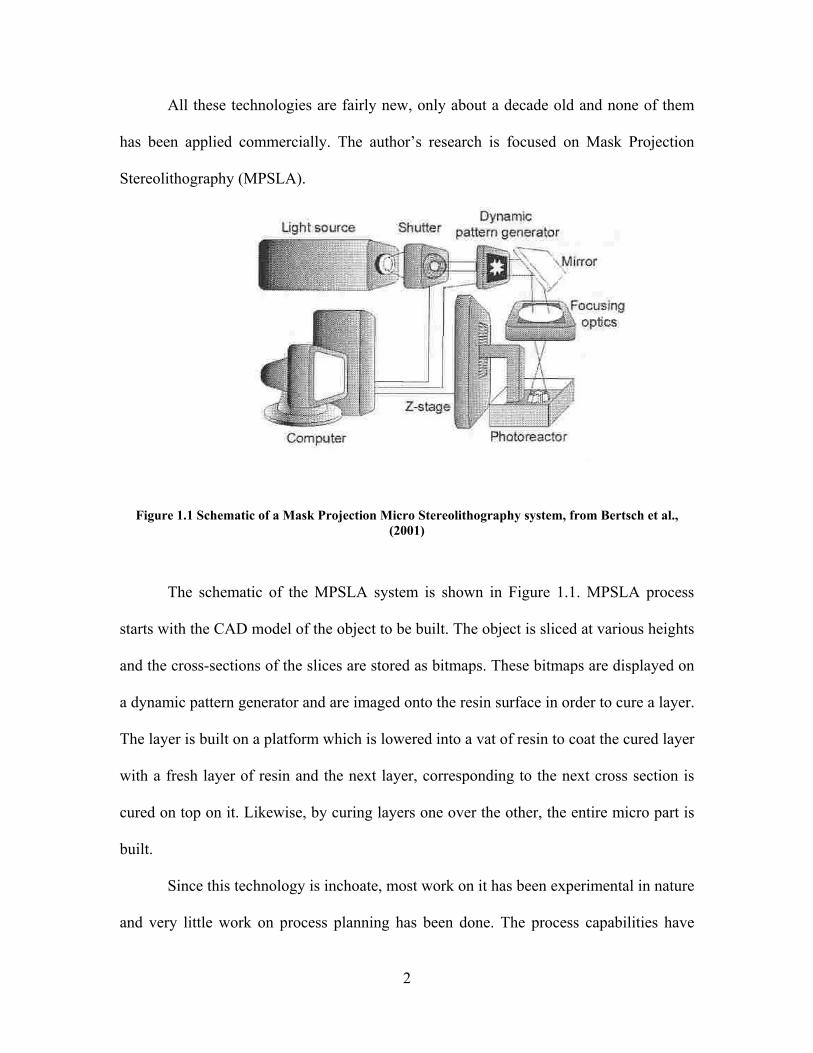
Figure 1.1 Schematic of a Mask Projection Micro Stereolithography system, from Bertsch et al., (2001)
The schematic of the MPSLA system is shown in Figure 1.1. MPSLA process
starts with the CAD model of the object to be built. The object is sliced at various heights
and the cross-sections of the slices are stored as bitmaps. These bitmaps are displayed on
a dynamic pattern generator and are imaged onto the resin surface in order to cure a layer.
The layer is built on a platform which is lowered into a vat of resin to coat the cured layer
with a fresh layer of resin and the next layer, corresponding to the next cross section is
cured on top on it. Likewise, by curing layers one over the other, the entire micro part is
built.
Since this technology is inchoate, most work on it has been experimental in nature
and very little work on process planning has been done. The process capabilities have

3
been demonstrated by building very high resolution 3D parts. However, analytical
modeling of this process has not been done. In order to mature this technology into a high
resolution manufacturing process, it needs to be studied in more detail. The author’s
research is focused on analyzing the MPSLA process and formulating a process planning
method, which will enable the selection of the values of the process parameters to build
the part of interest.
The need for a greater understanding of Mask Projection Stereolithography has
been accentuated by its adoption by the additive manufacturing companies. Desktop 3D
printers by 3D SystemsTM , Desktop FactoryTM and Envision TecTM are expected to flood
the low cost prototyping market in the near future. These printers are based on the
MPSLA technology.
In Section 1.1, an introduction to Micro-Stereolithography has been provided. In
Section 1.2, the status of research in MPSLA and in process planning for additive
manufacturing technologies has been reviewed and the areas where research is needed are
identified. In Section 1.3, the research objective for this PhD is scoped out. In Section
1.4, the organization of this dissertation is presented.
1.1 Micro Stereolithography
The Stereolithography process is explained in Section 1.1.1. The adaptations of
this process for micro fabrication have been presented in Section 1.1.2. In Section 1.1.3,
the advantages the Mask Projection approach over the other adaptations is presented.

4
1.1.1 Stereolithography
The Stereolithography process begins with the definition of a CAD model of the
desired object, followed by slicing of the three dimensional (3-D) model into a series of
very closely spaced horizontal planes that represent the X-Y cross sections of the 3-D
object, each with a slightly different Z-coordinate value. All the cross-sections are then
translated into a numerical control code and merged together into a build file. This build
file is used to control the ultraviolet (UV) light scanner and Z-axis translator. The desired
polymer object is then “written” into the UV-curable resist, layer by layer, until the entire
structure has been defined.
The schematic of the Stereolithography process is shown in Figure 1.2
Figure 1.2 Schematic of a Stereolithography machine from Jacobs (1992)
The basic elements of a Stereolithography system are as follows:
• Laser Optics System,
• Scanning System,

5
• Elevator and Recoater, and
• Computer Control and Software
The laser optics system consists of the laser used to cure the resin and the beam
shaping optics. The beam shaping optics is responsible for conditioning the laser beam
and focusing it on the resin surface with the desired spot size.
The scanning system consists of a set of galvanometric mirrors, which direct the
laser beam so that the required cross-section is scanned.
The elevator lowers the cured layer by a distance of one layer thickness. The
recoater coats a fresh layer of resin on the cured layer. This layer is then scanned by the
laser.
Computer and the controlling software are used to control the galvanometric
mirrors. The computer also synchronizes the motion of laser, elevator and recoater.
When light is incident on a Stereolithography resin, it polymerizes.
Polymerization is the process of linking small molecules (monomers) into larger
molecules (polymers) comprised of many monomer units. Most Stereolithography resins
contain the vinyl monomers and acrylate monomers. Vinyl monomers are broadly
defined as monomers containing a carbon-carbon double bond. Acrylate monomers are a
subset of the vinyl family with the carboxylic acid group (-COOH) attached to the
carbon-carbon double bond. For an acrylate resin system, the usual catalyst is a free
radical. In Stereolithography, the radical is generated photo chemically. The source of the
photo chemically generated radical is a photo initiator, which reacts with an actinic
photon as shown in the photo-polymerization scheme presented in Figure 1.3. This
produces radicals (indicated by a large dot) that catalyze the polymerization process.

6
Figure 1.3 Scheme of the photo-polymerization process (Jacobs, 1992)
1.1.2 Three approaches to Micro-Stereolithography
When Stereolithography is used to fabricate micro-parts, it is called Micro
Stereolithography. The principle of Micro Stereolithography is the same as
Stereolithography, i.e. “Writing a cross section on a photopolymer surface by means of
UV light”. However, the resolution required of a Micro-Stereolithography process is
much finer.
Micro-Stereolithography technologies developed so far can be divided into three
categories:
• Scanning Micro-Stereolithography
• Two photon polymerization, and
• Mask Projection Micro-Stereolithography, or Integral Micro-Stereolithography
1.1.2.1 Scanning Micro-Stereolithography Systems The scanning optical system of the conventional Stereolithography machine
introduces errors in the build. Also, the spot size doesn’t remain constant throughout the
layer cross-section. As a result, the resolution and accuracy are low. In scanning Micro-

7
Stereolithography, this drawback is eliminated by keeping the light beam focused onto a
stationary tight spot and scanning the layer by moving the work piece under the spot.
The principle of Scanning Micro-Stereolithography is shown in Figure 1.4.
Figure 1.4 Principle of Scanning Micro-Stereolithography from Beluze et al., (1999)
Scanning Micro-Stereolithography systems have been presented in literature in
(Nakamoto et al., 1996; Maruo and Kawata, 1998). The following specifications of a
typical scanning Micro-Stereolithography process have been presented in (Gardner,
Varadan, Awadelkarim, 2001)
• 5 µm spot size of the UV beam
• Positional accuracy is 0.25 µm (in the X-Y directions) and 1.0 µm in the Z-
direction.
• Minimum size of the unit of harden polymer is 5 µm x 5 µm x 3 µm (in X, Y, Z).

8
• Maximum size of fabrication structure is 10mm x 10mm x 10mm.
1.1.2.2 Two photon polymerization When near IR light, with a high peak power is focused inside a resin, the spatial
density of photons becomes high at the focal point. Each initiator in the two photon
absorbing (TPA) resin absorbs two near IR photons at the same time and becomes a
radical. Resultant radicals break double bonds of carbon in acrylyl group in the
monomers and oligomers and successively create new radicals at the ends of these
monomers and oligomers. Radicals combine with another monomer. This chain reaction
continues till chained radical meets another chained radical. The polymerization
mechanism is shown in Figure 1.5.
Figure 1.5 Photo chemical reaction for two-photon micro-fabrication. From (Maruo et al., 1997)
Two-photon polymerization (TPP) has been successfully used to fabricate parts
with lateral resolution as small as 200nm (Stute et al., 2003).
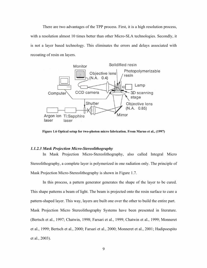
The schematic of the TPP system realized by Maruo et al., (1997) is shown in
Figure 1.6. They used a Ti Sapphire laser, with wavelength 790nm, pulse-width 200fs,
and peak power 50kW. The objective lens had an NA = 0.85. The micro part was scanned
bottom up.
9
There are two advantages of the TPP process. First, it is a high resolution process,
with a resolution almost 10 times better than other Micro-SLA technologies. Secondly, it
is not a layer based technology. This eliminates the errors and delays associated with
recoating of resin on layers.
Figure 1.6 Optical setup for two-photon micro fabrication. From Maruo et al., (1997)
1.1.2.3 Mask Projection Micro-Stereolithography In Mask Projection Micro-Stereolithography, also called Integral Micro
Stereolithography, a complete layer is polymerized in one radiation only. The principle of
Mask Projection Micro-Stereolithography is shown in Figure 1.7.
In this process, a pattern generator generates the shape of the layer to be cured.
This shape patterns a beam of light. The beam is projected onto the resin surface to cure a
pattern-shaped layer. This way, layers are built one over the other to build the entire part.
Mask Projection Micro Stereolithography Systems have been presented in literature.
(Bertsch et al., 1997; Chatwin, 1998; Farsari et al., 1999; Chatwin et al., 1999; Monneret
et al., 1999; Bertsch et al., 2000; Farsari et al., 2000; Monneret et al., 2001; Hadipoespito
et al., 2003).

10
Figure 1.7 Principle of Mask Projection Micro-Stereolithography
1.1.3 Advantages of Mask Projection approach over Scanning approach
The Mask Projection Micro-Stereolithography process has the following
advantages over Scanning Micro-Stereolithography.
• The light flux density arriving on the surface of the photopolymerizable resin
when projecting the image of a complete layer is low compared to the one of a
light beam accurately focused in one point. As a result there are no problems of
unwanted polymerizations due to thermal effect.
• Mask Projection Micro-Stereolithography processes are faster than the scanning
processes because vector-by-vector scanning is a slower process. The TPP

11
process is very slow because the spot size of the laser used is very small (~200-
400nm).
• The accuracy of integral process is also better because the errors introduced by
the X-Y translation stages are avoided. The only mobile element in these systems
is the Z-Stage.
Due to these advantages, the author’s research is focused on Mask Projection
Stereolithography.
1.2 Literature review
The status of research in the field of MPSLA is presented in Section 1.2.1. A
review of the research done in process planning for other Rapid Prototyping technologies
is presented in Section 1.2.2. Areas which need to be researched are identified in Section
1.2.3.
1.2.1 Status of research in MPSLA
Complex 3D parts cured by MPSLA have been presented in literature by various
research groups (Figure 1.8). The specifications of their systems are presented in Table
1.1.
12
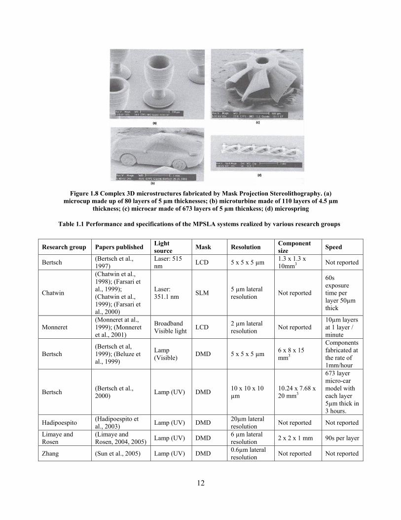
Figure 1.8 Complex 3D microstructures fabricated by Mask Projection Stereolithography. (a) microcup made up of 80 layers of 5 µm thicknesses; (b) microturbine made of 110 layers of 4.5 µm
thickness; (c) microcar made of 673 layers of 5 µm thicnkess; (d) microspring
Table 1.1 Performance and specifications of the MPSLA systems realized by various research groups
Research group Papers published Light source Mask Resolution Component
size Speed
Bertsch (Bertsch et al., 1997)
Laser: 515 nm LCD 5 x 5 x 5 µm 1.3 x 1.3 x
10mm3 Not reported
Chatwin
(Chatwin et al., 1998); (Farsari et al., 1999); (Chatwin et al., 1999); (Farsari et al., 2000)
Laser: 351.1 nm SLM 5 µm lateral
resolution Not reported
60s exposure time per layer 50µm thick
Monneret (Monneret at al., 1999); (Monneret et al., 2001)
Broadband Visible light LCD 2 µm lateral
resolution Not reported 10µm layers at 1 layer / minute
Bertsch (Bertsch et al, 1999); (Beluze et al., 1999)
Lamp (Visible) DMD 5 x 5 x 5 µm 6 x 8 x 15
mm3
Components fabricated at the rate of 1mm/hour
Bertsch (Bertsch et al., 2000) Lamp (UV) DMD 10 x 10 x 10
µm 10.24 x 7.68 x 20 mm3
673 layer micro-car model with each layer 5µm thick in 3 hours.
Hadipoespito (Hadipoespito et al., 2003) Lamp (UV) DMD 20µm lateral
resolution Not reported Not reported
Limaye and Rosen
(Limaye and Rosen, 2004, 2005) Lamp (UV) DMD 6 µm lateral
resolution 2 x 2 x 1 mm 90s per layer
Zhang (Sun et al., 2005) Lamp (UV) DMD 0.6µm lateral resolution Not reported Not reported
13
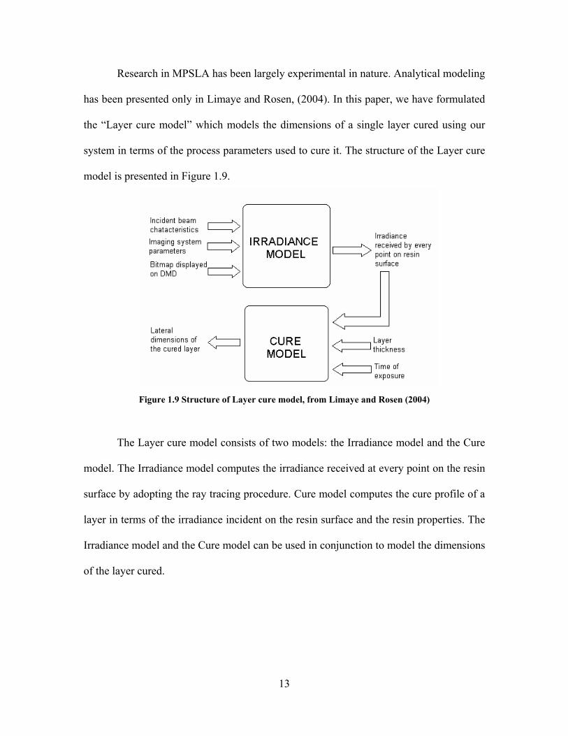
Research in MPSLA has been largely experimental in nature. Analytical modeling
has been presented only in Limaye and Rosen, (2004). In this paper, we have formulated
the “Layer cure model” which models the dimensions of a single layer cured using our
system in terms of the process parameters used to cure it. The structure of the Layer cure
model is presented in Figure 1.9.
Figure 1.9 Structure of Layer cure model, from Limaye and Rosen (2004)
The Layer cure model consists of two models: the Irradiance model and the Cure
model. The Irradiance model computes the irradiance received at every point on the resin
surface by adopting the ray tracing procedure. Cure model computes the cure profile of a
layer in terms of the irradiance incident on the resin surface and the resin properties. The
Irradiance model and the Cure model can be used in conjunction to model the dimensions
of the layer cured.
14
1.2.2 Process planning in other additive manufacturing technologies
Process planning has been done for various RP processes with different
objectives, like reducing dimensional errors, improving surface finish and reducing build
time. In this section, this literature has been reviewed.
Dimensional accuracy
The most common source of errors in the vertical dimensions of
Stereolithography builds is print through. Print through is caused by the addition of
residual energies from separate laser scans exceeding the photo polymerization threshold
of the resin. This problem has been addressed in commercial Stereolithography machines
by adopting the “Layer compensation” approach. Here, the lowest layer of a part being
built is skipped in order to compensate for the increase in dimension that would occur
due to print through (AccuMaxTM Toolkit User Guide, 1996).
Lynn-Charney and Rosen (2000) empirically modeled geometric tolerances of
Stereolithography builds in terms of process parameters. They considered six types of
geometric tolerances: positional, flatness, parallelism, perpendicularity, concentricity and
circularity. Response surfaces (Myers and Montgomery, 1995) were constructed to relate
these tolerances with various process parameters.
Surface finish
Surface finish is rougher along the z-axis of RP parts than parallel to the xy-plane
because of the “stair stepping” effect (Paul and Voorakarnam, 2001). It is most prominent
when the surface orientation is not orthogonal to the slice’s vertical profile. The cusp
height is considered as a measure of the surface finish of a RP prototype in the vertical
direction. Cusp height is the maximum surface deviation due to stair stepping effect and

15
is directly dependent on the layer thickness and orientation angle. Suh and Wozny,
(1994) formulated an analytical relation between the cusp height and the layer thickness
to determine the maximum allowable layer thickness that would satisfy the constraint on
cusp height.
Reduction in layer thicknesses leads to an increase in build time. Sabourin et al.,
(1996) addressed this problem by stepwise uniform refinement. They proposed using
thinner slices only where the vertical profile is highly curved, while using thicker slices
everywhere else, thereby reducing the build time. Mani et al., (1999) proposed region
based adaptive slicing, where only the portion of layers adjacent to the edge of the part
are sliced with smaller layer thicknesses while the interiors are composed of thicker
layers. (Figure 1.10)
Figure 1.10 Region based adaptive slicing and traditional adaptive slicing (Mani et al., 1999)
Reeves and Cobb, (1997) expressed surface roughness of RP parts as a function of
surface angle (θ ), layer thickness (α ) and layer profile (φ ), as shown in Figure 1.11, to
obtain the following expression for surface roughness of up- and down-facing surfaces.

16
Figure 1.11 Nomenclature used by Reeves and Cobb (1997)
Ra K
Ra K
up
down
=+
+
=− − + −
+
α φ θ θ
α φ θ θ
(tan sin cos )
(tan( )sin( ) cos( )4
180 1804
1
(1.1)
where K and K1 are factors determined experimentally.
Reeves and Cobb, (1997) observed that the surface finish of the down facing
surfaces was much better than that predicted by their analytical model. They attribute this
effect to ‘print through’. As shown in Figure 1.12, print through causes a partial “fillet”
between two layers causing a modification to the layer profile and hence, reducing the
surface deviation.
Sager and Rosen (2005) formulated a process planning method to cure smooth
down facing SLA surfaces by controlling the scan parameters (laser velocity and pitch of
scan). They discretized the down facing surface into an array of points and chose process
parameters in such a way that the sum of squares of the deviations of the exposures
received by these points from the threshold exposure was minimized.

17
Figure 1.12 Surface smoothing caused by print through. From Reeves and Cobb, (1997)
Build time
Chen and Sullivan, (1996) formulated an algorithm to predict build time of
Stereolithography parts by using detailed scan and recoat information from the build
files. Other researchers have also quantified build time. All of them have broken down
the part building process into its constituent steps and modeled the time required to
complete each of these steps.
1.2.3 Identifying areas where research is needed
In this subsection, the areas in which research needs to be done in order to mature
the MPSLA technology into a MEMS packaging technology are identified.
Dimensional accuracy of the 3D MPSLA part
In Limaye and Rosen, (2004), the dimensional accuracy of a single layer cured
using MPSLA has been quantified. However, the accuracy in all the three dimensions of
a MPSLA part has not been studied. While tolerances can be empirically expressed in
terms of process parameters by conducting numerous experiments as done by Lynn-
Charney and Rosen, (2000) this would require numerous experiments to have enough

18
confidence in the response surfaces. Analytically relating the errors in dimensions to
the process parameter values would aid process planning to a large extent.
The Layer compensation approach in commercial SLA systems to compensate for
errors in vertical dimensions is an ad-hoc approach that would work only if the down
facing surface is horizontal and the print through is exactly equal to the thickness of the
lowermost (skipped) layer. A more rigorous approach to avoid print through errors,
applicable to parts of any geometry is needed.
Surface finish of MPSLA builds
Extensive research has been done on improving the surface finish of laser-
scanning Stereolithography. The relation between layer thicknesses and surface finish has
already been formulated by numerous researchers. This can be adapted to MPSLA.
Though print through smoothing phenomenon has been observed in Stereolithography by
Reeves and Cobb (1997), it has not been successfully employed to obtain smoother down
facing surfaces due to lack of control offered by SLA machines. “The size of the print
through fillet is related to the laser energy initiating photo polymerization, which is, in
turn affected by both laser power and scan speed. If either or both of these process
attributes could be varied, then the size of the fillet could be modified and matched to
surface angle, hence producing smoother down facing surfaces. In reality, both scan
speed and laser power are complex attributes of the SLA process and out of control of the
SL user” (Reeves and Cobb, 1997). MPSLA process can achieve the gray scaling of the
irradiance pattern required for print through smoothing. Analytical model relating the
gray scaling of irradiance pattern projected onto the resin surface with the surface
finish is needed.

19
Process planning
Process planning under multiple conflicting objectives has been done by Lynn-
Charney and Rosen (2000) and West et al. (2001), for commercial Stereolithography
process. A similar process planning method needs to be formulated for MPSLA.
1.3 Research Objective
In this research, the author seeks to address the research areas identified in
Section 1.2.3. In this section, a motivating problem is provided that integrates all the
research areas mentioned above.
Micro nozzles have numerous applications. Apart from their current use in printer
heads, their usage is envisaged as propelling devices for micro/nano satellites, as micro
fuel injectors and for numerous other micro fluidic applications. Micro nozzles are
currently fabricated by bulk etching techniques by etching a trench of the shape of the
nozzle in the plane of a wafer and anodically bonding glass on both sides (Bayt and
Breuer, 2000) or by etching a ‘via’ in silicon using anisotropic etch (Meacham et al.,
2004). However, these fabrication techniques cannot fabricate micro nozzles with any
geometry in any orientation. Mask Projection Stereolithography can be used for this
purpose.
20
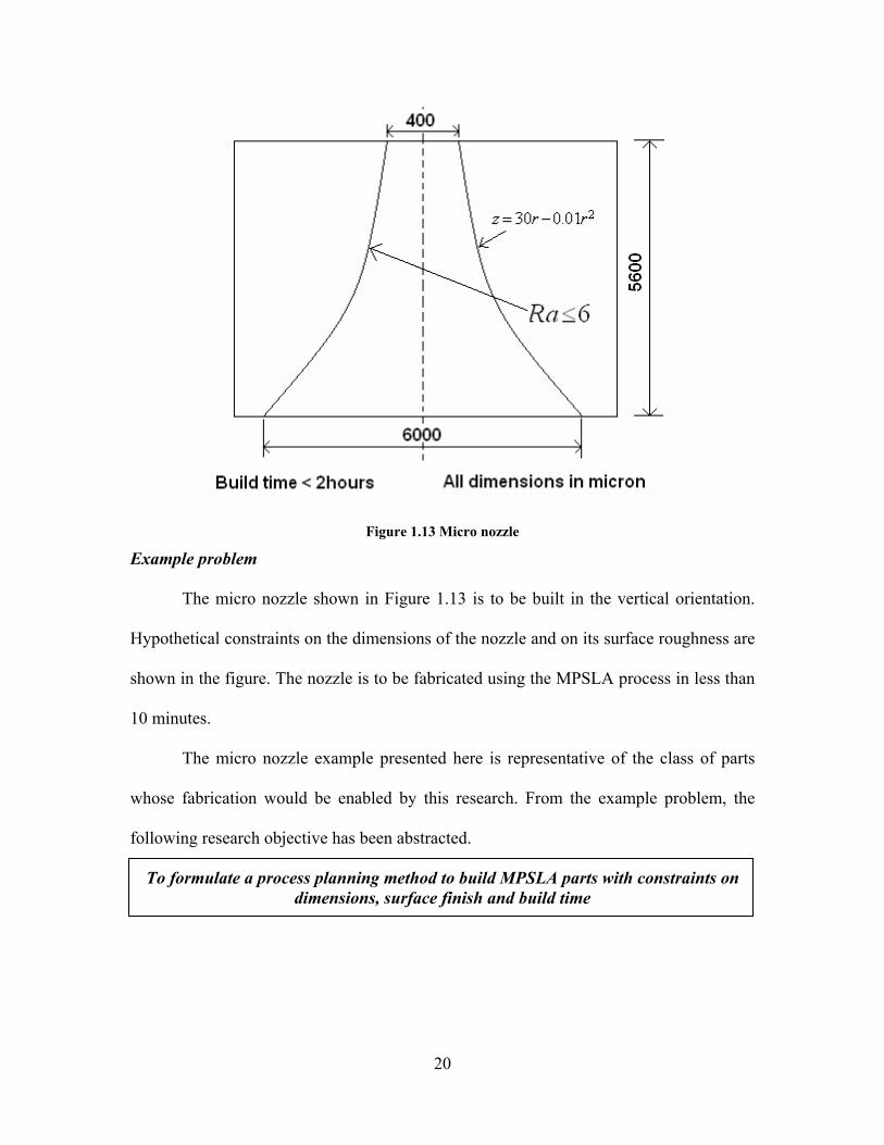
Figure 1.13 Micro nozzle
Example problem
The micro nozzle shown in Figure 1.13 is to be built in the vertical orientation.
Hypothetical constraints on the dimensions of the nozzle and on its surface roughness are
shown in the figure. The nozzle is to be fabricated using the MPSLA process in less than
10 minutes.
The micro nozzle example presented here is representative of the class of parts
whose fabrication would be enabled by this research. From the example problem, the
following research objective has been abstracted.
To formulate a process planning method to build MPSLA parts with constraints on dimensions, surface finish and build time

21
1.4 Organization of this dissertation
The research objective scoped out in Section 1.3 is realized in this dissertation by
completing the tasks as expressed in Figure 1.14. A MPSLA system is realized as a part
of this research. The part building process is modeled by adopting a multi-scale modeling
strategy. This model is used to do process planning to achieve objectives of dimensional
accuracy, build time and surface finish. The work done in achieving these three
objectives in integrated to formulate a multi-objective process planning method that
would allow a user to obtain trade-offs between these objectives. As shown in Figure
1.14, there are three research questions that would have to be addressed in order to
complete these tasks. Hypotheses are formulated and tested for each of these research
questions.
In Chapter 2, the foundational knowledge and theory necessary to achieve the
research objective is presented.
In Chapter 3, the design of the MPSLA system realized as a part of this research
is presented.
In Chapter 4, the research objective is broken down into research questions and
hypotheses are formulated for these research questions. Strategies to test these hypotheses
are formulated in this chapter.
In Chapter 5, the “Irradiance model” is formulated. This model computes the
irradiance received by the resin surface when a given bitmap is imaged onto it for a given
time. The Irradiance model is validated by building test layers on the MPSLA system.
In Chapter 6, the Print through model is formulated, which computes the print
through that would occur underneath a multi- layered part. The Print through model is
22
used to formulate the Compensation zone approach is introduced to avoid print through
errors introduced when layers are cured over each other. The Compensation zone
approach is demonstrated by building test parts.
In Chapter 7, the Adaptive exposure method is formulated which can be used to
cure downward facing surfaces accurately and with a good surface finish. A slicing
algorithm is presented to enable a process planner slice a 3D CAD file in order to achieve
the required tradeoffs between objectives of build time and surface finish of up facing
surfaces is formulated
In Chapter 8, the work presented in Chapters 5, 6 and 7 is integrated to formulate
a process planning method to build MPSLA parts with constraints on dimensions, surface
finish and build time is formulated. This process planning method is demonstrated on a
test part with quadratic up facing and down facing surfaces.
In Chapter 9, the research questions are re-visited and the contributions of this
work are summarized. The limitations of the work and directions for future work are also
discussed.

23
Figure 1.14 Organization of this dissertation
Summary
In this chapter, the motivation to analytically model the Mask Projection
Stereolithography process and formulate a process planning method for the same is
presented. Literature review has been presented on Mask Projection Stereolithography
and on process planning for other additive manufacturing processes. The organization of
chapters in this dissertation has been presented.

24
CHAPTER 2 FOUNDATIONS FOR FORMLULATING PROCESS PLANNING METHOD FOR MASK PROJECTION STEREOLITHOGRAPHY
In this chapter, the foundational knowledge required to analytically model the
MPSLA process is presented. The fundamentals of image formation are discussed in
Section 2.1. The fundamentals of resin curing are presented in Section 2.2.
2.1 Fundamentals of image formation
During the irradiation step, a bitmap displayed on the DMD is imaged onto the
resin surface. Modeling the irradiance on the resin surface is, essentially, modeling the
process of image formation by the imaging lens. There are two possible ways of
modeling the process of image formation: by assuming wave nature of light; and by
assuming ray nature of light. In the first case, diffraction analysis is used, while, if the
second assumption is considered valid, then geometric optical analysis is used to model
the image formed. In this section, both the methods of analysis are presented.
If the imaging system is ‘perfect’, i.e. free of aberrations, then diffraction analysis
should be used. If the imaging system is imperfect, i.e. has significant aberrations, then,
geometric optical analysis is to be used. This section also presents the conditions that
have to be satisfied in order for either of these analyses to be used.
2.1.1 Diffraction (Physical optics) analysis
In diffraction analysis, light is considered to be propagating as waves. When light
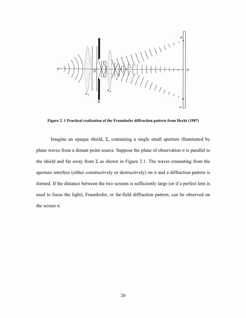
passes through an aperture in an opaque screen, it gets diffracted. If the diffracted pattern
is observed far away from the screen, then, the Fraunhofer diffraction pattern is observed.
The distance between the aperture and the image plane, for observing Fraunhofer
25
diffraction is very large. A practical method of realizing this diffraction pattern is to use a
convex lens to focus the diffraction pattern onto the screen. Fraunhofer diffraction pattern
is generated by the lens. The Fraunhofer diffraction pattern can be shown to be the
Fourier transform of the aperture function. Thus, the lens is considered as a Fourier
transformer.
In this section, apart from presenting formulae, the derivations explaining the role
of a lens as a Fourier transformer are also presented in order to highlight the assumptions
that are made in these derivations. It is important to be aware of these assumptions while
evaluating the validity of using diffraction analysis to model image formation in practical
situations. In Section 2.1.1.1, the Fraunhofer diffraction pattern for light passing through
an aperture is derived. In Section 2.1.1.2, the Fraunhofer diffraction pattern is shown to
be the Fourier transform of the aperture function. In Section 2.1.1.3, the role of a
converging lens as a Fourier transformer is presented.
2.1.1.1 Fraunhofer diffraction Physical optics assumes that light propagates in the form of wavefronts. Huygen-
Fresnel principle states that: “Every unobstructed point of a wavefront at a given instant
in time, serves as a source of spherical secondary wavelets (with the same frequency as
that of the primary wave). The amplitude of the optical field at any point beyond is the
superposition of all these wavelets (considering their amplitudes and relative phases)”.
26
Figure 2. 1 Practical realization of the Fraunhofer diffraction pattern from Hecht (1987)
Imagine an opaque shield, Σ, containing a single small aperture illuminated by
plane waves from a distant point source. Suppose the plane of observation σ is parallel to
the shield and far away from Σ as shown in Figure 2.1. The waves emanating from the
aperture interfere (either constructively or destructively) on σ and a diffraction pattern is
formed. If the distance between the two screens is sufficiently large (or if a perfect lens is
used to focus the light), Fraunhofer, or far-field diffraction pattern, can be observed on
the screen σ.

27
Derivation of Fraunhofer diffraction from an aperture
Figure 2.2 Fraunhofer diffraction from an arbitrary aperture where r and R and very large compared to the size of the hole, from Hecht (1987)
Consider the configuration depicted in Figure 2.2. A monochromatic plane wave
propagating in the x-direction is incident on the opaque diffracting screen Σ. We wish to
find the consequent (far-field) flux-density distribution in space, or equivalently at some
arbitrary point P. According to the Huygens-Fresnel principle, a differential area dS,
within the aperture may be envisioned as being covered with coherent secondary point
sources. But dS is much smaller in extent than λ so that contributions at P from dS remain
in phase and interfere constructively. If ε A is the source strength per unit area, assumed
to be constant over the entire aperture, then the optical disturbance at P due to dS is the
real part of
dEr
e dSA i t kr= −ε ω( ) (2.1)
where k = 2π λ/
28
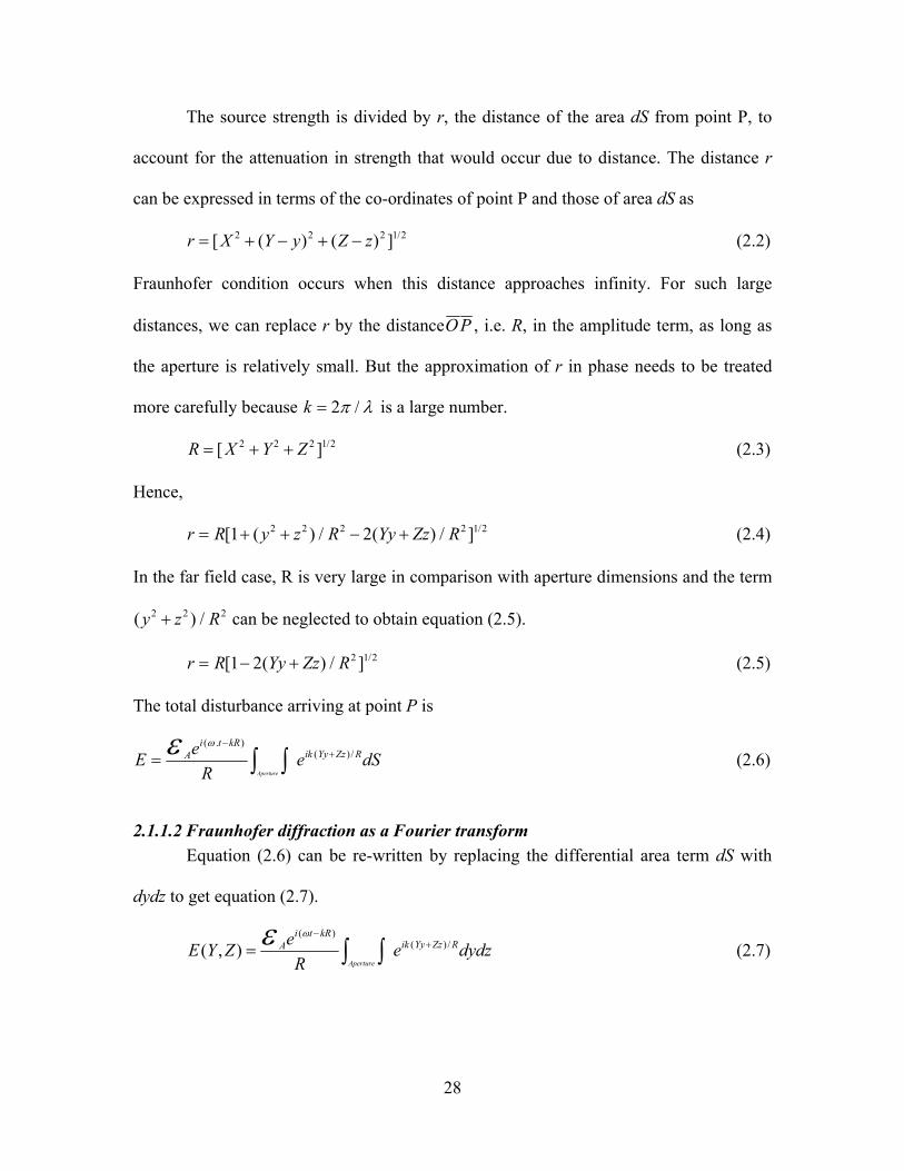
The source strength is divided by r, the distance of the area dS from point P, to
account for the attenuation in strength that would occur due to distance. The distance r
can be expressed in terms of the co-ordinates of point P and those of area dS as
r X Y y Z z= + − + −[ ( ) ( ) ] /2 2 2 1 2 (2.2)
Fraunhofer condition occurs when this distance approaches infinity. For such large
distances, we can replace r by the distanceO P , i.e. R, in the amplitude term, as long as
the aperture is relatively small. But the approximation of r in phase needs to be treated
more carefully because k = 2π λ/ is a large number.
R X Y Z= + +[ ] /2 2 2 1 2 (2.3)
Hence,
r R y z R Yy Zz R= + + − +[ ( ) / ( ) / ] /1 22 2 2 2 1 2 (2.4)
In the far field case, R is very large in comparison with aperture dimensions and the term
( ) /y z R2 2 2+ can be neglected to obtain equation (2.5).
r R Yy Zz R= − +[ ( ) / ] /1 2 2 1 2 (2.5)
The total disturbance arriving at point P is
E eR
e dSAi t kR
ik Yy Zz R
Aperture
=−
+zzε ω( . )( )/ (2.6)
2.1.1.2 Fraunhofer diffraction as a Fourier transform Equation (2.6) can be re-written by replacing the differential area term dS with
dydz to get equation (2.7).
E Y Z eR
e dydzAi t kR
ik Yy Zz R
Aperture( , )
( )( )/=
−+zzε ω
(2.7)

29
If we limit ourselves to a small region in space over which R is essentially constant,
everything in front of the integral, with the exception of ε A , can be lumped together. ε A
could vary within the aperture and can be expressed by the complex quantity
A y z A y z ei y z( , ) ( , ) ( , )= 0φ (2.8)
which is called as the aperture function. The amplitude of the field over the aperture is
described by A y z0 ( , ) while the point to point phase variation is represented by ei y zφ ( , ) .
Accordingly, A y z dydz( , ) is proportional to the diffracted field emanating from the
differential source element dydz . Consolidating this much, we can reformulate equation
(2.8) more generally as
E Y Z A y z e dydzik Yy Zz R( , ) ( , ) ( )/= +
−∞
+∞
−∞
+∞zz (2.9)
The limits on the integral can be extended to ±∞ because the aperture function is nonzero
only over the region of the aperture.
Let us define spatial frequencies kY and kZ as
k kY RY = / (2.10)
and
k kZ RZ = / (2.11)
The diffracted field (equation 2.9) can now be written as
E k k A y z e dydzY Zi k y k zY Z( , ) ( , ) ( )= +
−∞
+∞
−∞
+∞zz (2.12)
Equation 2.12 can be immediately recognized to be the Fourier transform of A y z( , ).
Thus, the derivation proves that: the field distribution in the Fraunhofer diffraction
pattern is the Fourier transform of the field distribution across the aperture (i.e. the
aperture function). Symbolically, this is written as
30
E k k F A y zY Z( , ) { ( , )}= (2.13)
2.1.1.3 Lens as a Fourier transformer
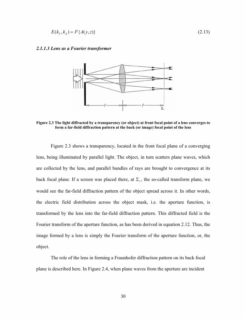
Figure 2.3 The light diffracted by a transparency (or object) at front focal point of a lens converges to form a far-field diffraction pattern at the back (or image) focal point of the lens
Figure 2.3 shows a transparency, located in the front focal plane of a converging
lens, being illuminated by parallel light. The object, in turn scatters plane waves, which
are collected by the lens, and parallel bundles of rays are brought to convergence at its
back focal plane. If a screen was placed there, at Σ t , the so-called transform plane, we
would see the far-field diffraction pattern of the object spread across it. In other words,
the electric field distribution across the object mask, i.e. the aperture function, is
transformed by the lens into the far-field diffraction pattern. This diffracted field is the
Fourier transform of the aperture function, as has been derived in equation 2.12. Thus, the
image formed by a lens is simply the Fourier transform of the aperture function, or, the
object.
The role of the lens in forming a Fraunhofer diffraction pattern on its back focal
plane is described here. In Figure 2.4, when plane waves from the aperture are incident
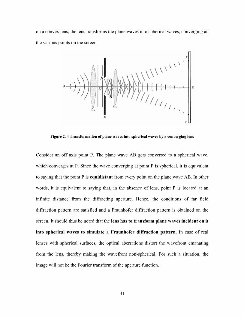
31
on a convex lens, the lens transforms the plane waves into spherical waves, converging at
the various points on the screen.
Figure 2. 4 Transformation of plane waves into spherical waves by a converging lens
Consider an off axis point P. The plane wave AB gets converted to a spherical wave,
which converges at P. Since the wave converging at point P is spherical, it is equivalent
to saying that the point P is equidistant from every point on the plane wave AB. In other
words, it is equivalent to saying that, in the absence of lens, point P is located at an
infinite distance from the diffracting aperture. Hence, the conditions of far field
diffraction pattern are satisfied and a Fraunhofer diffraction pattern is obtained on the
screen. It should thus be noted that the lens has to transform plane waves incident on it
into spherical waves to simulate a Fraunhofer diffraction pattern. In case of real
lenses with spherical surfaces, the optical aberrations distort the wavefront emanating
from the lens, thereby making the wavefront non-spherical. For such a situation, the
image will not be the Fourier transform of the aperture function.
32
Another important consideration is related to the waves that are incident on the
lens from the aperture. If they are not plane waves then again, there is an error introduced
in the wavefront emanating beyond the lens. Further, the light from the aperture has to be
monochromatic and coherent in order to obtain Fraunhofer diffraction pattern.
2.1.2 Image modeling by Geometric Optics
In this section, an alternative approach to modeling the image formation by an
imaging system is presented. This approach assumes that light travels in the form of rays,
as opposed to waves. This theory is valid in case of aberration limited optical systems. In
Section 2.1.2.1, an introduction to optical aberrations is provided. In Section 2.1.2.2, the
concept of Optical Path Difference (OPD) is introduced as the parameter which is used to
quantify the extents of optical aberrations present in an optical system. In Section 2.1.2.3,
the exact ray tracing procedure, used to model imaging in an aberration limited optical
system is presented.
2.1.2.1 Introduction to optical aberrations When a perfect lens focuses any object onto an image plane, all rays emanating
from any one point on the object meet at one and the same point on the image. Under this
condition, the image formed is termed as the perfect image. For a thin lens, this
condition occurs when the image distance (i) and the object distance (o) are related to the
focal length (f) of the lens by the thin lens equation:
1/i – 1/o = 1/f (2.14)
The magnification of the image is given by M = – (i/o).
33
For a spherical lens with a finite thickness, even if the image and object distances are set
as calculated using the thin-lens equation, all rays from any one point on the object do not
converge to the same point on the image. Also, the focal length of a spherical lens is not
the same for all object points. This results in optical aberrations. Optical aberrations can
be thought of as imperfections caused in an image. They lead to the formation of a
distorted image, with lower contrast. Aberrations are classified as follows:
• Spherical aberration
• Astigmatism
• Coma
• Distortion
• Chromatic aberration
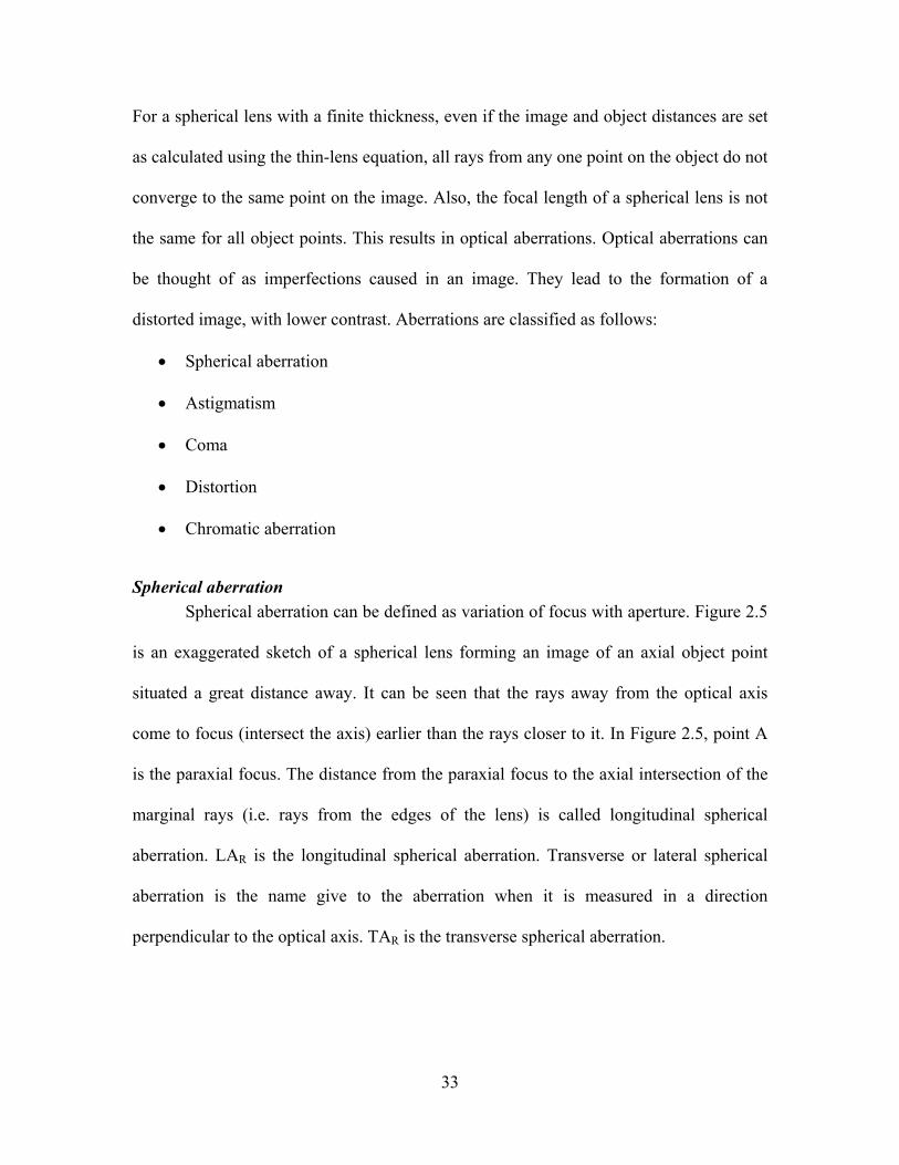
Spherical aberration Spherical aberration can be defined as variation of focus with aperture. Figure 2.5
is an exaggerated sketch of a spherical lens forming an image of an axial object point
situated a great distance away. It can be seen that the rays away from the optical axis
come to focus (intersect the axis) earlier than the rays closer to it. In Figure 2.5, point A
is the paraxial focus. The distance from the paraxial focus to the axial intersection of the
marginal rays (i.e. rays from the edges of the lens) is called longitudinal spherical
aberration. LAR is the longitudinal spherical aberration. Transverse or lateral spherical
aberration is the name give to the aberration when it is measured in a direction
perpendicular to the optical axis. TAR is the transverse spherical aberration.

34
Figure 2.5 Spherical aberration from Smith, (1990)
Coma Coma can be defined as variation in magnification with aperture. When a bundle
of oblique rays is incident on a lens with coma, the rays passing through the edge
portions of the lens are imaged at a different height than those passing through the center
portion. In Figure 2.6, the upper and lower rim rays A and B intersect the image plane
above the ray P which passes through the center of the lens. The distance from P to the
intersection of A and B is called tangential coma of the lens.
ComaT = HAB - Hp
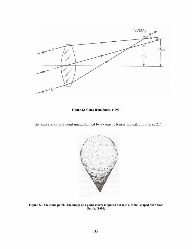
35
Figure 2.6 Coma from Smith, (1990)
The appearance of a point image formed by a comatic lens is indicated in Figure 2.7.
Figure 2.7 The coma patch. The image of a point source is spread out into a comet-shaped flare from Smith, (1990)

36
Astigmatism Any plane through the optical axis is called as the meridional, or the tangential
plane. The imaginary plane passing through the chief ray (an oblique ray passing through
a point on the object and the center of the lens) and perpendicular to the meridional plane
is called the sagittal plane. All the rays from the object, which lie in this plane, are called
sagittal rays. See Figure 2.8.
Astigmatism occurs when the tangential and the sagittal images don’t coincide. In
the presence of astigmatism, the image of a point source is not a point, but takes the form
of two separate lines as shown in Figure 2.8.
Unless there is some manufacturing defect in a lens, there is no astigmatism when an
axial point is imaged. However, as the imaged point moves farther from the axis, the
amount of astigmatism gradually increases.
Figure 2.8 Astigmatism from Smith, (1990)
37
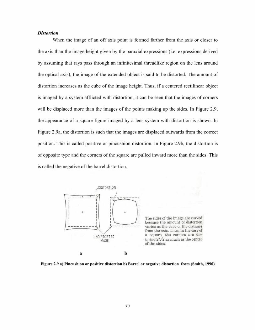
Distortion When the image of an off axis point is formed farther from the axis or closer to
the axis than the image height given by the paraxial expressions (i.e. expressions derived
by assuming that rays pass through an infinitesimal threadlike region on the lens around
the optical axis), the image of the extended object is said to be distorted. The amount of
distortion increases as the cube of the image height. Thus, if a centered rectilinear object
is imaged by a system afflicted with distortion, it can be seen that the images of corners
will be displaced more than the images of the points making up the sides. In Figure 2.9,
the appearance of a square figure imaged by a lens system with distortion is shown. In
Figure 2.9a, the distortion is such that the images are displaced outwards from the correct
position. This is called positive or pincushion distortion. In Figure 2.9b, the distortion is
of opposite type and the corners of the square are pulled inward more than the sides. This
is called the negative of the barrel distortion.
Figure 2.9 a) Pincushion or positive distortion b) Barrel or negative distortion from (Smith, 1990)
a b
38
Chromatic Aberration These aberrations can be understood intuitively. Chromatic aberrations are caused
because the refractive index of any material is different for different wavelengths of
lights.
The above section described the aberrations in terms of the inability of a lens to
focus down all rays at the ideal image points. When we consider light as waves
propagating along these rays, their relative phases are not the same as would be expected
in case of a far field diffraction pattern. It is interesting to note the effects of aberrations
on the relative phase differences in the various waves arriving at a point, from the point
of view of questioning the validity of the optical analysis method. The aberrations are
described in terms of the distortions produced in a wavefront in the next section.
2.1.2.2 Wavefront aberrations The optical aberrations cause deformations in the wavefront. The extent of these
deformations can be used as a quantitative measure for deciding which modeling strategy
to use. If these deformations are minor, then aberrations analysis can be used to augment
the diffraction analysis presented earlier. If the deformations in wavefronts however are
very large, then, geometric optics should be used.
The extent of the variation of the deformed wavefront from its actual shape is
denoted by measuring the “Optical Path Difference”, or OPD. In this section, the OPD
introduced by a system having spherical aberrations is derived to explain the meaning of
OPD.
39
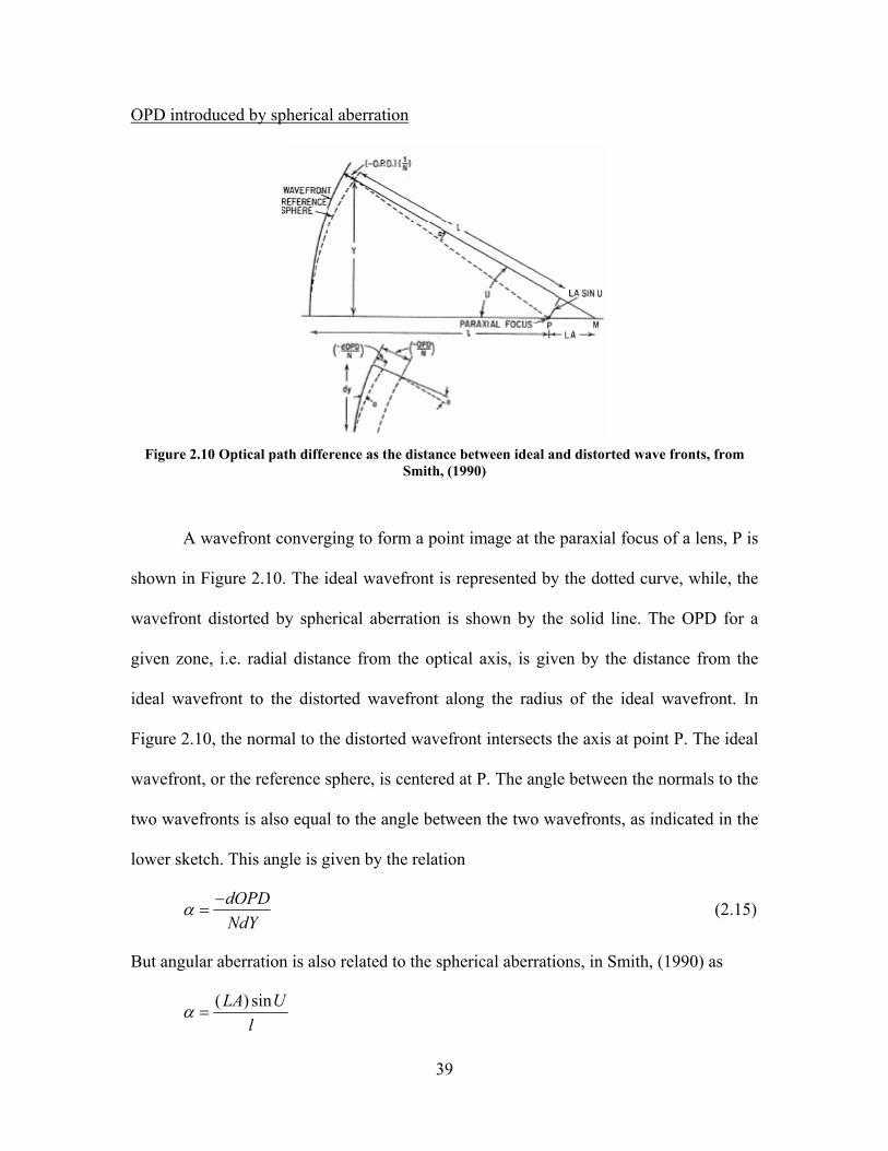
OPD introduced by spherical aberration
Figure 2.10 Optical path difference as the distance between ideal and distorted wave fronts, from
Smith, (1990)
A wavefront converging to form a point image at the paraxial focus of a lens, P is
shown in Figure 2.10. The ideal wavefront is represented by the dotted curve, while, the
wavefront distorted by spherical aberration is shown by the solid line. The OPD for a
given zone, i.e. radial distance from the optical axis, is given by the distance from the
ideal wavefront to the distorted wavefront along the radius of the ideal wavefront. In
Figure 2.10, the normal to the distorted wavefront intersects the axis at point P. The ideal
wavefront, or the reference sphere, is centered at P. The angle between the normals to the
two wavefronts is also equal to the angle between the two wavefronts, as indicated in the
lower sketch. This angle is given by the relation
α =−dOPD
NdY (2.15)
But angular aberration is also related to the spherical aberrations, in Smith, (1990) as
α =( ) sinLA U
l

40
= ( )LA Yl2 (2.16)
By combining and solving for dOPD, we get
dOPD YN LA dYl
=− ( )
2 (2.17)
Longitudinal spherical aberrations can be represented by the series
LA aY bY cY= + + +2 4 6 ....
For most optical systems, the spherical aberration is almost entirely of the third order and
can be expressed as
LA aY= 2
Making this substitution and integrating throughout the zone of radius Y, we get
OPD NYl
aY dYY
= −z 20
2( )
= −NYl
aY2
2
2
2 2. (2.18)
= −12 2
22
N U aYsin ( )
At the edge of the aperture, Y=Ym and LA=LAm, (the subscript denoting marginal ray and
marginal longitudinal spherical aberration). Substitute the value of a as:
a LAY
m
m
= 2 (2.19)
Thus,
OPD N U LA YYm
m
=−14
2 2sin ( )[ ] (2.20)
Equation (2.20) gives the OPD caused only because of spherical aberrations. Real
optical systems have numerous lenses and stops in series and introduce numerous kinds

41
of aberrations apart from spherical. Analytical computation of the OPD in the distorted
wavefront that would occur due to the combined presence of all these aberrations is a
non-trivial task and can be performed by means of some optical analysis software.
It is clear from the preceding discussion that the size and shape of an image
formed by a lens is not intuitive. Due to optical aberrations, the thin lens equation will
calculate erroneous dimensions of the aerial image formed on the resin surface. The exact
image size can be calculated by adopting the procedure of tracing rays through a lens as
explained in the next sub-section.
2.1.2.3 Exact ray tracing From Section 2.1.2.1, it is clear that the size of the expected image cannot be
determined from the simple lens equation. The exact size of the image can be obtained
through “exact ray tracing procedures.” In an exact ray trace, the object is considered as a
collection of point sources. Rays in all possible directions are traced from each of these
point sources. The rays undergo refraction at every surface separating two media. The
refraction is governed by Snell’s law:
sin i / n1 = sin i’/n2, (2.21)
where i and i’ are the angles of incidence and refraction, and n1 and n2 are the refractive
indices of the media on either side of the surface on which the rays are incident. By
tracing rays, their points of intersection with the image plane are calculated. The farthest
points of intersections give the size and shape of the image.
Exact ray tracing is an involved procedure, especially because the angle of
incidence (i) for every ray is in a different plane. In this section, the ray tracing procedure
42
presented in (Smith, 1990) is described. This ray tracing procedure was first published by
D. Feder in the Journal of the Optical Society of America vol. 41, pp. 630-636, 1951.
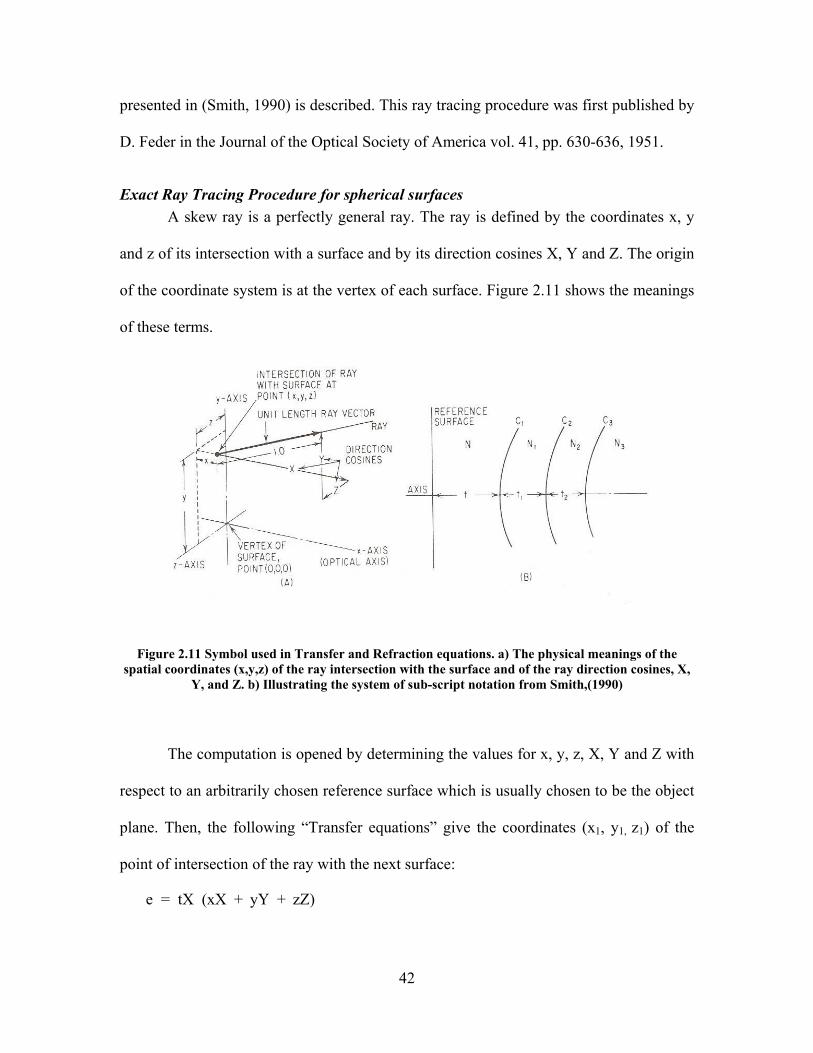
Exact Ray Tracing Procedure for spherical surfaces A skew ray is a perfectly general ray. The ray is defined by the coordinates x, y
and z of its intersection with a surface and by its direction cosines X, Y and Z. The origin
of the coordinate system is at the vertex of each surface. Figure 2.11 shows the meanings
of these terms.
Figure 2.11 Symbol used in Transfer and Refraction equations. a) The physical meanings of the spatial coordinates (x,y,z) of the ray intersection with the surface and of the ray direction cosines, X,
Y, and Z. b) Illustrating the system of sub-script notation from Smith,(1990)
The computation is opened by determining the values for x, y, z, X, Y and Z with
respect to an arbitrarily chosen reference surface which is usually chosen to be the object
plane. Then, the following “Transfer equations” give the coordinates (x1, y1, z1) of the
point of intersection of the ray with the next surface:
e = tX (xX + yY + zZ)

43
M x ex t1x = + −
M x y z e t 2tx12 2 2 2 2 2= + + − + −
E X c (c M 2M )12
1 1 12
1x= − −
L e (c M 2M ) / (X E )1 12
1x 1= + − +
x x LX t1 = + −
y y LY1 = +
z z LZ1 = +
The direction cosines of a ray after it undergoes refraction at a surface are given by the
following “Refraction equations”:
E1'
1 22
121 (N / N ) (1 E )= − −
g E (N / N )E1 1'
1 1= −
X (N / N )X g c x g1 1 1 1 1 1= − +
Y (N / N )Y g c y1 1 1 1 1= −
Z (N / N )Z g c z1 1 1 1 1= −
In the above Transfer and Refraction equations, the symbols have the following
meanings:
t Distance between two surfaces
x,y,z The spatial coordinates of the ray intersection with the
reference surface

44
x ,y ,z1 1 1 The spatial coordinates of the ray intersection with surface #1
M1 The distance (vector) from the vertex of surface # 1 to the ray,
perpendicular to the ray
M1x The x component of M1
E1 The cosine of the angle of incidence at surface #1
L The distance along the ray from the reference surface (x, y, z)
to surface #1 (x1, y1, z1)
E1' The cosine of the angle of refraction (I’) at surface #1
X, Y, Z The direction cosines of the ray in space between the reference
surface and surface #1 (before refraction)
X , Y , Z1 1 1 The direction cosines after refraction by surface #1
c The curvature (reciprocal radius = 1/R) of the reference surface
c1 The curvature of surface #1
N The refractive index between the reference surface and surface
#1
N' The refractive index following surface #1
T The axial spacing between the reference surface and surface #1
2.1.3 Selection of modeling strategy
In Sections 2.1.1 and 2.1.2, two strategies of modeling the image formation
process have been presented: Physical Optics, which assumes the wave nature of light,

45
and Geometric Optics, which assumes the ray nature of light. The selection of the Optical
modeling strategy would depend upon the kind of optical system that is being used.
2.1.3.1 When to use Physical Optics? Physical Optics can be used to model image formation is the system is
“diffraction limited”. Goodman (1968) says that “an imaging system is said to be
diffraction limited if a diverging spherical wave, emanating from a point-source object, is
converted by the system into a new wave, again perfectly spherical, that converges
towards an ideal point in the image plane. Thus, the terminal property of a diffraction
limited lens system is that a diverging spherical wave is mapped into a converging
spherical wave at the exit pupil. For any real imaging system, this property will, at best
be satisfied over only a finite region of the object plane. If the object is confined to that
region, the system may be regarded as diffraction limited”.
Rayleigh Quarter-wave limit
The effect of optical aberrations is to distort the wave emerging from an optical
system from its ideal spherical shape. The Rayleigh quarter wave limit is used as a
measure of the amount of distortion that can be tolerated, for diffraction analysis to be
used. According to Rayleigh, there is no appreciable deterioration of image if the phase
differences introduced do not exceed π/2. In other words, the image quality is not
seriously impaired if the wavefront aberration does not exceed λ/4. If the wavefront
aberrations are within the Rayleigh quarter wave limit, then diffraction analysis is used.
In order to secure this high degree of correction, it is usually necessary to employ a
complicated and expensive optical system.
46
2.1.3.2 When to use Geometric Optics? Geometric optics is used for modeling image formation if the aberrations
introduced by the imaging system are significant. When the thin lens and the paraxial
approximations are not valid, the aberrations become significant. In such cases,
diffraction theory cannot be used. Goodman (1968) states: “The conclusion that a lens
composed of spherical surfaces maps an incident plane wave into a spherical wave is
dependent on the paraxial approximation. Under nonparaxial conditions the emerging
wavefront will exhibit departures from perfect sphericity (called aberrations) even if the
surfaces of the lens are perfectly spherical.”
The optical aberrations cause deformations in the wavefront which are not
accounted for in Physical optics. The extent of these deformations can be used as a
quantitative measure for deciding which modeling strategy to use. If these deformations
are minor, then aberrations analysis can be used to augment the diffraction analysis
presented earlier. If the deformations in wavefronts however are very large, then,
Geometric optics should be used. The choice of modeling strategy is summarized well in
Smith, (1990) as: “for small departures from perfection (i.e. aberrations which cause a
deformation of wavefront amounting to less than one or two wavelengths), it is
appropriate to consider the manner in which an aberration affects the distribution of
energy in the diffraction pattern. For larger amounts of aberration, however, the
illumination distribution, as described by raytracing can yield a quite adequate
representation of the performance of the [optical] system. Thus, it is convenient to divide
the considerations into (1) the effects of small amounts of aberration, which we treat in
terms of the wave nature of light, and (2) the effects of large amounts of aberration,
which may be treated geometrically.”
47
2.2 Fundamentals of resin curing
In this section, the chemistry behind the photo polymerization reactions that occur
when a Stereolithography resin cures is presented. Most commercial Stereolithography
resins are a mixture of acrylic monomers and epoxy resins. The acrylic monomers are
polymerized using a process called “Free Radical Photopolymerization”, while the epoxy
resins are cured using a process called “Cationic Photopolymerization”. The curing
mechanism of a commercial Stereolithography resin (SL 7510) is proposed in Rosen,
(2002). In this section, the curing mechanism of a commercial resin containing a mixture
of acrylates and epoxies is explained in Section 2.2.1. The Beer Lambert’s law of
radiation attenuation and the threshold model of resin cure is presented in Section 2.2.2.
2.2.1 Curing mechanism of commercial Stereolithography resins
Commercial SLA resins are a mixture of acrylates, epoxies, radical photo
initiators and cationic photoinitiators. When radiant energy is incident upon the resin, the
photoinitiators initiate polymerization reactions. In addition to these constituents, the
resins also contain photosensitizers, which increase the UV absorbance and increase the
initiation efficiency. The mechanisms of polymerization for acrylate and epoxy resins are
different. The “Free Radical Photopolymerization” mechanism of curing of acrylate
resins is described in Section 2.2.1.1. The “Cationic Photopolymerization” mechanism of
curing of epoxy resins is presented in Section 2.2.1.2. The polymer network formation is
discussed in Section 2.2.1.3.
2.2.1.1 Free Radical Photopolymerization Polymerization is the process of linking small molecules (monomers) into larger
molecules (polymers) comprised of many monomer units. Most Stereolithography resins

48
contain the vinyl monomers and acrylate monomers. Vinyl monomers are broadly
defined as monomers containing a carbon-carbon double bond. Acrylate monomers are a
subset of the vinyl family with the carboxylic acid group (-COOH) attached to the
carbon-carbon double bond. For an acrylate resin system, the usual catalyst is a free
radical. In Stereolithography, the radical is generated photo chemically. The source of the
photo chemically generated radical is a photo initiator, which reacts with an actinic
photon as shown in the photo-polymerization scheme presented in Figure 2.12. This
produces radicals (indicated by a large dot) that catalyze the polymerization process.
Figure 2.12 Scheme of the photo-polymerization process (Jacobs, 1992)
The free radical photopolymerization of acrylate systems is very fast, but of lower
density. This process is exothermic which is beneficial for activating the heat activated
cationic photoinitiators.
2.2.1.2 Cationic Photopolymerization The most important cationic photoinitiators are the onium salts, particularly the
triarylsulphonium and diaryliodonium salts. The photodecomposition mechanism of
triarylsulphonium is described in Rosen, (2002). When light is incident on the cationic

49
photointiator, a Bronted acid (H+X-) is generated by photolysis. The Bronsted acid acts as
a catalyst for the polymerization of the epoxide groups. The polymerization occurs by a
chain reaction, initiated by a protonated epoxide group. The termination of the chain
reaction is not immediate. The cationic polymerization once initiated continues over a
period of few hours to even a few days. It is speculated in Rosen, (2002) that hydroxyl
compounds are added to the mixture to terminate the chain reaction.
2.2.1.3 Interpenetrating polymer network formation When the acrylate and epoxy groups polymerize, they form their respective
networks. In the presence of each other, an interpenetrating network gets formed. An
interpenetrating network is defined as a combination of two polymers in network form, at
least one of which is synthesized and/or cross linked in the immediate presence of the
other. Thus, the polymers are formed in network form, and are not just mechanically
mixed. The formations of the acrylate and epoxy networks influence each other’s
formation. The reaction of acrylates increases the photospeed, reduces the energy
requirements of the epoxy reaction and also reduces the inhibitory effects of humidity on
the epoxy polymerization. The epoxy monomers also favor the acrylate
photopolymerization reaction. The epoxy monomer acts as a plasticizer, which increases
the molecular mobility, which favors the acrylate chain reaction. Further, the acrylate is
less sensitive to oxygen in a hybrid acrylate-epoxy system.
2.2.2 Beer Lambert’s law of light absorption
As the photons penetrate the resin, they are progressively absorbed by initiators.
According to Beer Lambert’s law of absorption, the exposure (mJ/cm2) decreases
exponentially with depth.
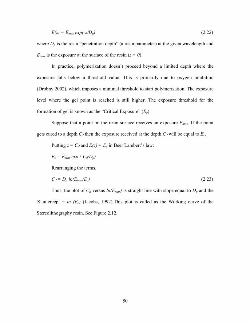
50
E(z) = Emax exp(-z/Dp) (2.22)
where Dp is the resin “penetration depth” (a resin parameter) at the given wavelength and
Emax is the exposure at the surface of the resin (z = 0).
In practice, polymerization doesn’t proceed beyond a limited depth where the
exposure falls below a threshold value. This is primarily due to oxygen inhibition
(Drobny 2002), which imposes a minimal threshold to start polymerization. The exposure
level where the gel point is reached is still higher. The exposure threshold for the
formation of gel is known as the “Critical Exposure” (Ec).
Suppose that a point on the resin surface receives an exposure Emax. If the point
gets cured to a depth Cd then the exposure received at the depth Cd will be equal to Ec.
Putting z = Cd and E(z) = Ec in Beer Lambert’s law:
Ec = Emax exp (-Cd/Dp)
Rearranging the terms,
Cd = Dp ln(Emax/Ec) (2.23)
Thus, the plot of Cd versus ln(Emax) is straight line with slope equal to Dp and the
X intercept = ln (Ec) (Jacobs, 1992).This plot is called as the Working curve of the
Stereolithography resin. See Figure 2.12.

51
Dp
ln(Ec) ln(E)
Cd
Figure 2.13 Theoretical Working curve of a Stereolithography resin
The values of Ec and Dp are fixed for any resin and so, the working curve of any
resin is, theoretically, invariant.
Summary
Analytically modeling the Mask Projection Stereolithography process entails
modeling the optical process of imaging a bitmap onto the resin surface and modeling the
curing process that occurs after the bitmap is imaged. The fundamental knowledge
related to optical imaging is presented in Section 2.1. Geometric optics and Physical
optics are the two theories that can be used for modeling image formation. The
assumptions made in these theories are presented and the method of image modeling
using both these methods is presented. In Section 2.2, the fundamentals of resin curing
has been presented. The polymerization mechanism of acrylate and epoxy based resins is
presented. The relation between the cure depth of a layer and the exposure supplied to it
is presented.

52
CHAPTER 3 DESIGN OF THE MASK PROJECTION STEREOLITHOGRAPHY SYSTEM
In this chapter, the design of the Mask Projection Stereolithography System
realized as a part of this research is presented. The primary modules of a MPSLA system
are identified in Limaye, (2004) as Collimation system; Imaging system; and Build
system. In this chapter, the design of all these systems is presented. In Section 3.1, the
requirements from the system to be designed are presented. In Section 3.2, the design of
every module is presented.
3.1 Requirements list
Prior to designing any system/machine, the performance requirements from that
system should be explicit identified. The requirements from the MPSLA system are
presented in Table 3.1. They are classified as “Demands”, which have to be fulfilled and
“Wishes”, whose fulfillment is preferred.
Table 3.1 Requirements list for the Mask Projection Stereolithography System
REQUIREMENTS LIST FOR THE MASK PROJECTON STEREOLITHOGRAPHY SYSTEM Formulated by Ameya Limaye
Demand/Wish Requirement Demand The largest cured layer dimension in one exposure should be greater than 10mm x 5 mm Demand The largest vertical dimension of a cured part should be greater than 5mm
Wish The distortions due to optical aberrations should be as less as possible Wish The lateral resolution should be better than 20µm Wish The vertical resolution of the system should be better than 100µm Wish The system should have as much depth of focus as possible
Demand The total cost of realizing the system should be less than $16000
3.2 Design of the MPSLA system
The optical schematic of a M PSLA system has been presented in Limaye,
(2004), as shown in Figure 3.1.

53
Figure 3.1 Optical Structure to embody
3.2.1 Collimating system
The function of the collimating system is to collect the diverging rays emerging
from the lamp and send out parallel or almost parallel rays. Rays parallel to the optical
axis reduce the Coma that would be introduced by the imaging system subsequently.
The light source should emit radiation in the UV range, mostly at around 365nm.
The light source selected is ADACTM System’s Cure Spot TM 50. This lamp emits 3000 +
mW/cm2 at 365 nm. The Spectral distribution of the lamp is as shown in Figure 3.2. The
typical half cone divergence angle of the light emitted from the light guide is given to be
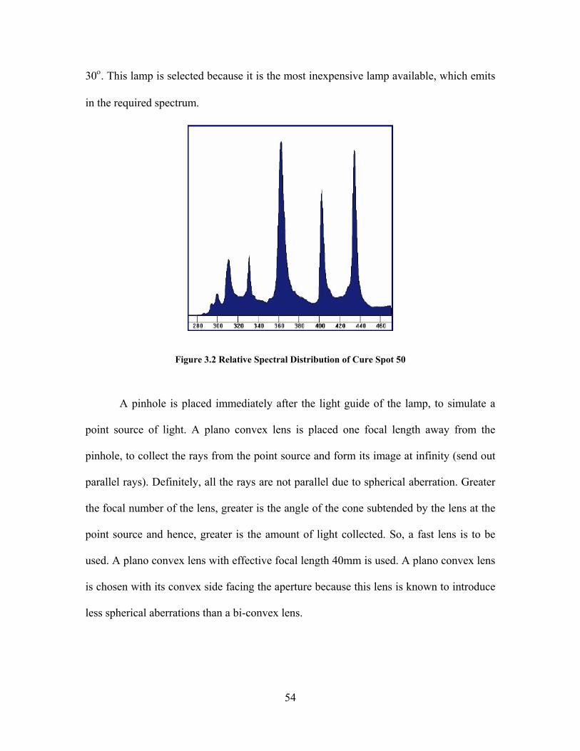
54
30ο. This lamp is selected because it is the most inexpensive lamp available, which emits
in the required spectrum.
Figure 3.2 Relative Spectral Distribution of Cure Spot 50
A pinhole is placed immediately after the light guide of the lamp, to simulate a
point source of light. A plano convex lens is placed one focal length away from the
pinhole, to collect the rays from the point source and form its image at infinity (send out
parallel rays). Definitely, all the rays are not parallel due to spherical aberration. Greater
the focal number of the lens, greater is the angle of the cone subtended by the lens at the
point source and hence, greater is the amount of light collected. So, a fast lens is to be
used. A plano convex lens with effective focal length 40mm is used. A plano convex lens
is chosen with its convex side facing the aperture because this lens is known to introduce
less spherical aberrations than a bi-convex lens.

55
A filter, allowing only 365nm wavelength to pass through, was placed after the
collimating lens. However, it was found that the light intensity coming out of the filter
was unacceptably low. So, the filter was removed from the system.
The final collimating system is shown in Figure 3.3
Figure 3.3 Collimating system
3.2.2 Imaging system
The function of the imaging system is to image the pattern displayed on the DMD
onto the photopolymer resin. The requirements for this system are that it should introduce
minimum optical aberrations; and it should give the best possible depth of focus and
lateral resolution. To minimize the optical aberrations and to increase the depth of focus,
a telecentric optic system is used.

56
Telecentric system
Figure 3.4 Imaging lens without a stop
Consider the lens shown in Figure 3.4. The lens itself acts as an aperture stop and
all the rays emanating from every object point, which are collected by the lens are
focused by the lens onto the image.
Figure 3.5 Stop placed at the focal point of the lens (Telecentric of the object side)
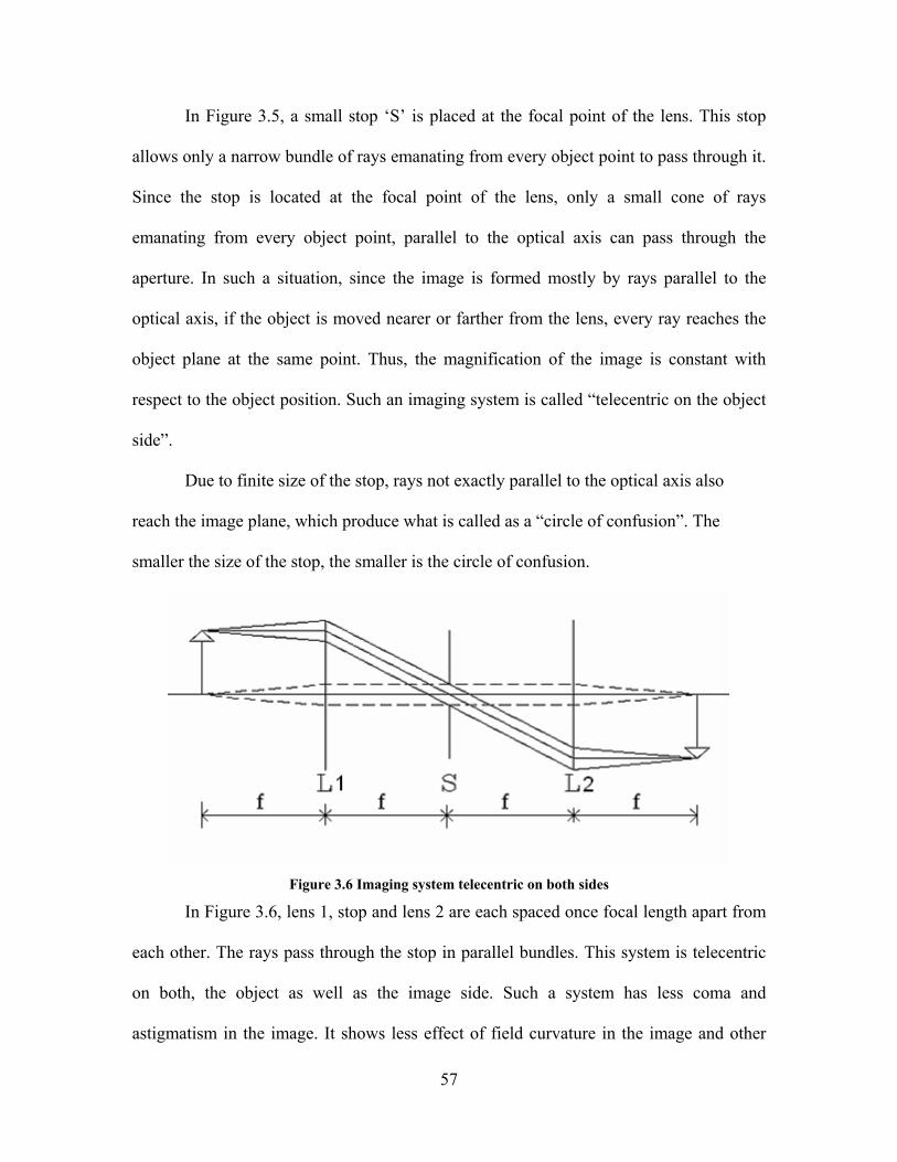
57
In Figure 3.5, a small stop ‘S’ is placed at the focal point of the lens. This stop
allows only a narrow bundle of rays emanating from every object point to pass through it.
Since the stop is located at the focal point of the lens, only a small cone of rays
emanating from every object point, parallel to the optical axis can pass through the
aperture. In such a situation, since the image is formed mostly by rays parallel to the
optical axis, if the object is moved nearer or farther from the lens, every ray reaches the
object plane at the same point. Thus, the magnification of the image is constant with
respect to the object position. Such an imaging system is called “telecentric on the object
side”.
Due to finite size of the stop, rays not exactly parallel to the optical axis also
reach the image plane, which produce what is called as a “circle of confusion”. The
smaller the size of the stop, the smaller is the circle of confusion.
Figure 3.6 Imaging system telecentric on both sides
In Figure 3.6, lens 1, stop and lens 2 are each spaced once focal length apart from
each other. The rays pass through the stop in parallel bundles. This system is telecentric
on both, the object as well as the image side. Such a system has less coma and
astigmatism in the image. It shows less effect of field curvature in the image and other
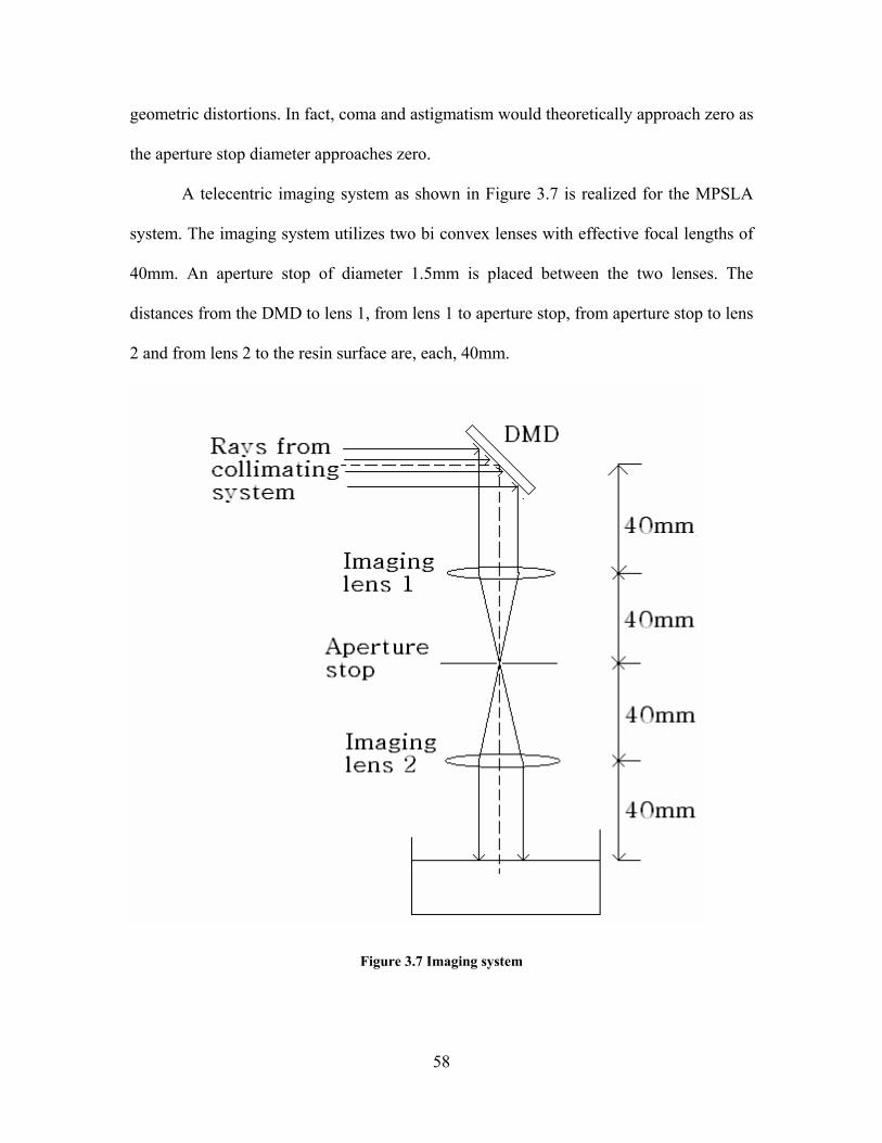
58
geometric distortions. In fact, coma and astigmatism would theoretically approach zero as
the aperture stop diameter approaches zero.
A telecentric imaging system as shown in Figure 3.7 is realized for the MPSLA
system. The imaging system utilizes two bi convex lenses with effective focal lengths of
40mm. An aperture stop of diameter 1.5mm is placed between the two lenses. The
distances from the DMD to lens 1, from lens 1 to aperture stop, from aperture stop to lens
2 and from lens 2 to the resin surface are, each, 40mm.
Figure 3.7 Imaging system

59
A system telecentric on both the sides has the following advantages for the
MPSLA system.
• The optical aberrations (coma, astigmatism, distortions) are minimized and hence
the layers are cured with fewer distortions.
• The system is more robust to variations in the resin level.
• The system is robust to the angular mounting of the DMD.
Mask
The Digital Micromirror Device (DMDTM) is an array of individually addressable,
bi-stable micro-mirrors (Dudley et al., 2003). A bitmap can be displayed on the DMD by
selectively orienting its mirrors in one direction. As opposed to the Liquid Crystal
Display (LCD) and Spatial Light Modulator (SLM), the DMD is a reflective mask. As a
mask, the DMD has advantages over LCD and SLM. The pixel density of the DMD is
higher because the mirrors are smaller in size than the LCD and SLM pixels (12.7µm
square as opposed to 24µm square in LCD and SLM) and also because the spacing
between mirrors is much less than that between the LCD and SLM pixels.
The DMD is mounted so as to direct the beam of light incident on it is reflected
downwards.

60
Figure 3.8 Digital micromirror device from Nayar et al., (2004)
3.2.3 Build System
The Build system consists of a vat and a platform mounted on a XYZ translation
stage. The platform can be translated vertically into the resin vat under computer control.
In addition, the platform can also be translated in the lateral direction. The translation
stage has a resolution of 100nm.
DSM SOMOS 10120 resin is used with this setup. This resin was used because it
was the lowest viscosity commercial Stereolithography resin that was readily available in
the laboratory.
The final system is as shown in Figure 3.9. The description of every component is
presented in Table 3.2.
Figure 3.9 Optical schematic of the MPSLA system realized as a part of this research
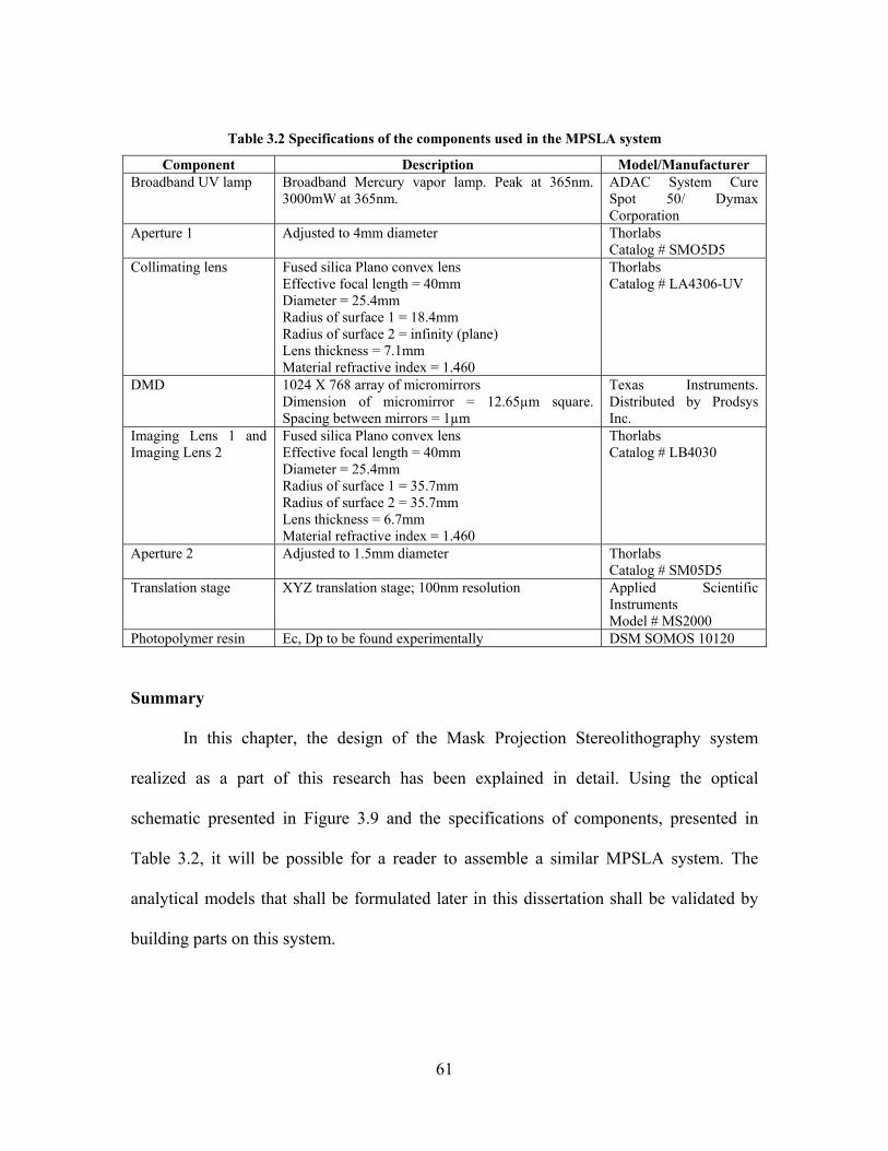
61
Table 3.2 Specifications of the components used in the MPSLA system
Component Description Model/Manufacturer Broadband UV lamp Broadband Mercury vapor lamp. Peak at 365nm.
3000mW at 365nm. ADAC System Cure Spot 50/ Dymax Corporation
Aperture 1 Adjusted to 4mm diameter Thorlabs Catalog # SMO5D5
Collimating lens Fused silica Plano convex lens Effective focal length = 40mm Diameter = 25.4mm Radius of surface 1 = 18.4mm Radius of surface 2 = infinity (plane) Lens thickness = 7.1mm Material refractive index = 1.460
Thorlabs Catalog # LA4306-UV
DMD 1024 X 768 array of micromirrors Dimension of micromirror = 12.65µm square. Spacing between mirrors = 1µm
Texas Instruments. Distributed by Prodsys Inc.
Imaging Lens 1 and Imaging Lens 2
Fused silica Plano convex lens Effective focal length = 40mm Diameter = 25.4mm Radius of surface 1 = 35.7mm Radius of surface 2 = 35.7mm Lens thickness = 6.7mm Material refractive index = 1.460
Thorlabs Catalog # LB4030
Aperture 2 Adjusted to 1.5mm diameter Thorlabs Catalog # SM05D5
Translation stage XYZ translation stage; 100nm resolution
Applied Scientific Instruments Model # MS2000
Photopolymer resin Ec, Dp to be found experimentally DSM SOMOS 10120
Summary
In this chapter, the design of the Mask Projection Stereolithography system
realized as a part of this research has been explained in detail. Using the optical
schematic presented in Figure 3.9 and the specifications of components, presented in
Table 3.2, it will be possible for a reader to assemble a similar MPSLA system. The
analytical models that shall be formulated later in this dissertation shall be validated by
building parts on this system.

62
CHAPTER 4 FORMULATION OF RESEARCH QUESTIONS AND HYPOTHESES
The research objective presented in Section 1.3 can be achieved by completing
the tasks proposed in Figure 1.14. The proposed research effort is explained in detail in
Sections 4.1 to 4.4. In Section 4.1, a multi scale modeling strategy for modeling the
exposure on the resin surface in terms of process parameters is proposed (Exposure
model). In Section 4.2, the compensation zone approach is proposed to cure
dimensionally accurate parts. In Section 4.3, an adaptation of the Compensation zone
approach to improve the surface finish of downward facing parts is proposed. In Section
4.4, the structure of a multi objective process planning method, which would enable the
building of MPSLA parts with requirements on dimensions, surface finish and build time,
is proposed.
In this chapter, research questions that need to be tackled in order to formulate a
process planning method for MPSLA are identified. Hypotheses to these research
questions are presented and tasks that will be undertaken to test these hypotheses are
enunciated.
4.1 Exposure modeling
4.1.1 Selection of optical modeling method
Image formation can be modeled in two ways. One is by assuming the wave
nature of light, and the principles of physical optics. The second is by assuming ray
nature of light and using the fundamentals of geometric optics. This leads us to the first
research question.

63
Research Question 1a Should the image formation process in the MPSLA system under
consideration by modeled using physical optics or using geometric optics?
Hypothesis The theory of geometric optics is more suitable than that of physical optics to
model the image formation by the MPSLA system under consideration.
Explanation
At a first glance, it seems that geometric optics should be used as opposed to
physical optics, because of the following reasons.
1. The light used in the setup is incoherent. A diffraction pattern is not obtained with
incoherent light.
2. The imaging system is expected to be aberration limited.
Tasks
As explained in Chapter 2, Section 2.1.3, physical optics theory should be used to
model image formation by a diffraction limited system, while the theory of geometric
optics should be used to model image formation by an aberration limited system. If the
Optical Path Difference (OPD), as explained in Section 2.1.2.2 is comparable with the
Rayleigh limit (λ/4), the system is diffraction limited and physical optics should be used
to model image formation. In case the OPD is several times the Rayleigh limit, the
imaging system is aberration limited. In order to test the hypothesis to Research Question
1a, the following tasks shall be performed
Task 1 Quantify the Optical Path Difference
The OPD introduced by the aberrations in the imaging system shall be quantified
to see if it exceeds the Rayleigh quarter wave limit by several times.
Task 2 Cure test layers

64
A ray tracing algorithm shall be formulated to obtain the exposure on the resin
surface given the bitmap to be imaged. A test bitmap shall be fed to this algorithm and
the lateral extents of the exposed region shall be measured. This bitmap shall be imaged
onto the resin surface for a long time and a layer will be cured. The lateral extents of the
exposed regions, returned by the algorithm, shall be compared with the lateral extents of
the cured layer. The extent agreement of the two results could shed some light on the
validity of using the geometric optics approach to image modeling.
4.1.2 Reducing the computational expense of ray-tracing approach
Ray tracing approach is a high fidelity approach which takes into account the
optical aberrations introduced by the imaging system and thereby accounts for the
distortions in the image and variation in irradiance across it that occurs due to
aberrations. The downside of the ray-tracing approach is that a large number of rays need
to be traced through the imaging system in order to converge to the irradiance profile on
the resin surface. If the model is to be implemented at a higher resolution, an even larger
number of rays would have to be traced. This leads us to our next research question.
Research Question 1b: How to model the exposure profile on the resin surface with the
fidelity of the ray tracing approach, in a computationally inexpensive way?
Hypothesis: A multi scale modeling approach can be adopted. The irradiance profile can
be thought of as a collection of pixels overlapping each other. Modeling should be done
at two levels:
1. Curing of individual pixels (computationally expensive part)
2. Overlapping of pixels to give the exposure profile on the resin surface
(computationally inexpensive part)

65
Explanation
Whenever any bitmap displayed on the DMD is imaged onto the resin surface,
every micro mirror in the “ON” state is imaged as a pixel on the resin surface. Depending
upon the time that a micro mirror is imaged, every pixel will get some exposure dose.
Thus, every micro mirror results in the exposure of a single pixel. Within a single layer,
adjacent pixels overlap each other laterally. The shape and dimensions of a pixel as well
as the exposure distribution across it will depend upon the location of the micromirror
exposing it, on the DMD.
It is proposed to model the exposure profile on the resin surface in two steps.
First, a ‘Pixel Image database’ shall be populated which would record the irradiance at
every pixel in terms of the optical parameters of the MPSLA system. Then, the Pixel
overlap model will be formulated that would compute the exposure profile on the resin
surface. The imaging of pixels, which is a computationally intensive process, will be
computed only once and a database recording the location and dimensions of every pixel,
including the irradiance distribution across it, shall be created. The proposed multi scale
strategy for modeling irradiance is shown in Figure 4.1.

66
Figure 4.1 Multi scale approach to model exposure
Tasks
In order to test this hypothesis, the following tasks shall be undertaken.
Task 1 Formulate the Pixel image model
First the resin surface shall be discretized into elements 10µm square each. In the
Pixel image model, rays will be traced from every micromirror on the DMD in all
directions. The lateral extents of the irradiated area (pixel) would encompass numerous
elements. The radiation (in mW/cm2) at these elements shall be stored in the pixel image
database. Let us denote the radiation received by the element (p,q) on the resin surface
due to rays emanating from the micromirror given by coordinates (a,b) as Hpq,ab. Suppose
the micromirror (a,b) is imaged for time Tab. Due to the radiation received solely from the
micromirror (a,b) for time Tab, the element (p,q) will receive an exposure dosage of Epq,ab
67
E H Tpq ab pq ab pq ab, , ,= × (4.1)
Task 2 Formulate the Pixel summation model
When pixels overlap laterally, they would share some element(s). At a shared
element, the total exposure would simply be the algebraic sum of the exposure it receives
from all the micromirrors that end up irradiating it. Suppose the element (p,q) is shared
between various pixels. Then, the irradiance at the element (p,q) due to the overlap is
given by equation 4.2.
E Epq pq ab= ∑ , with a,b across all the pixels which overlap at (p,q) (4.2)
Task 3 Test the model
The exposure profile obtained by imaging a test bitmap on the resin surface shall
be computed by using the multi-scale approach proposed above and the computational
time shall be quantified.
4.2 Curing dimensionally accurate parts
The first step towards curing a dimensionally accurate MPSLA part is to cure
dimensionally accurate layers. The lateral extents of every layer can be meshed with
pixels from the Pixel image database (Section 4.1.2) and then, the pixels can be mapped
onto the micromirrors on the DMD to generate the bitmap to be displayed on the DMD.
The next step is to determine the vertical dimension of the voxels that would be cured at
these pixels. The vertical dimensions of any Stereolithography part are prone to errors
because of print through errors.
When a layer is cured, radiation penetrates beyond its intended thickness. While
penetration of radiation beyond the layer is desirable in order to bind it to the layer
68
underneath it, the radiation also penetrates to the bottom surface of the part being built,
causing print-through errors. As the radiation propagates through the resin, it gets
attenuated according to the Beer Lambert’s law of absorption. The exposure received by
the resin at a depth z from the surface is given by
E z E e z Dp( ) /= −0 (4.3)
where E z( ) is the exposure at the depth z in resin,
E0 is the exposure at the resin surface,
Dp is the depth of penetration, which is a resin constant.
The resin beneath a MPSLA build gets exposed due to radiation penetrating to it from all
the layers cured above it. Exposure being additive, a point is reached when the exposure
received by the resin underneath the MPSLA part equals its threshold exposure for
polymerization (Ec). This unwanted curing causes an increase in the vertical dimension of
the part. This error is called as the print-through error. The source of print-through error
is depicted pictorially in Figure 4.2. The author aims to minimize the print through errors
through efficient process planning.
Research Question 2: How to reduce print through errors in MPSLA builds?
Hypothesis: Print through errors can be reduced by subtracting a tailored volume
(compensation zone) from underneath the CAD model which is used to build the part, in
such a way that the exposure received by the down facing surface of the part is exactly
equal to the threshold exposure of polymerization (Ec).
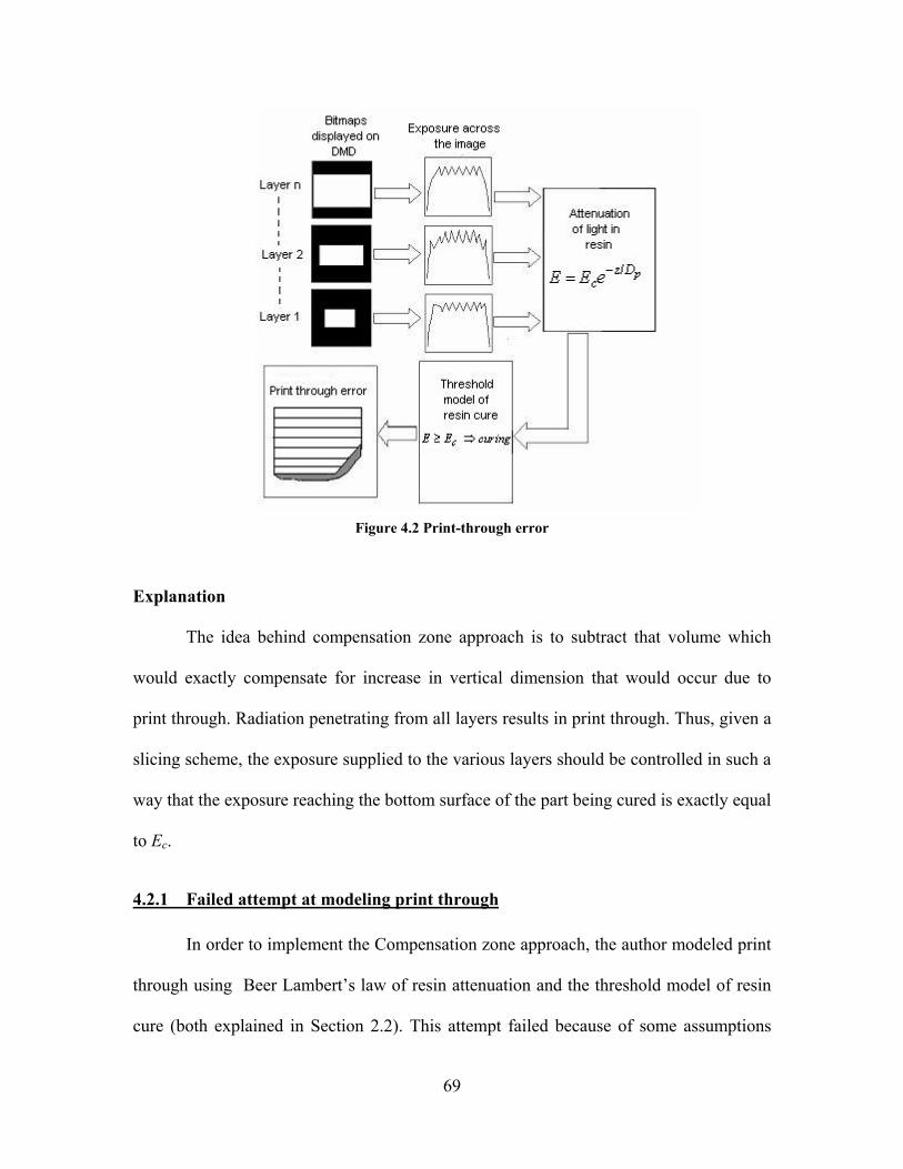
69
Figure 4.2 Print-through error
Explanation
The idea behind compensation zone approach is to subtract that volume which
would exactly compensate for increase in vertical dimension that would occur due to
print through. Radiation penetrating from all layers results in print through. Thus, given a
slicing scheme, the exposure supplied to the various layers should be controlled in such a
way that the exposure reaching the bottom surface of the part being cured is exactly equal
to Ec.
4.2.1 Failed attempt at modeling print through
In order to implement the Compensation zone approach, the author modeled print
through using Beer Lambert’s law of resin attenuation and the threshold model of resin
cure (both explained in Section 2.2). This attempt failed because of some assumptions
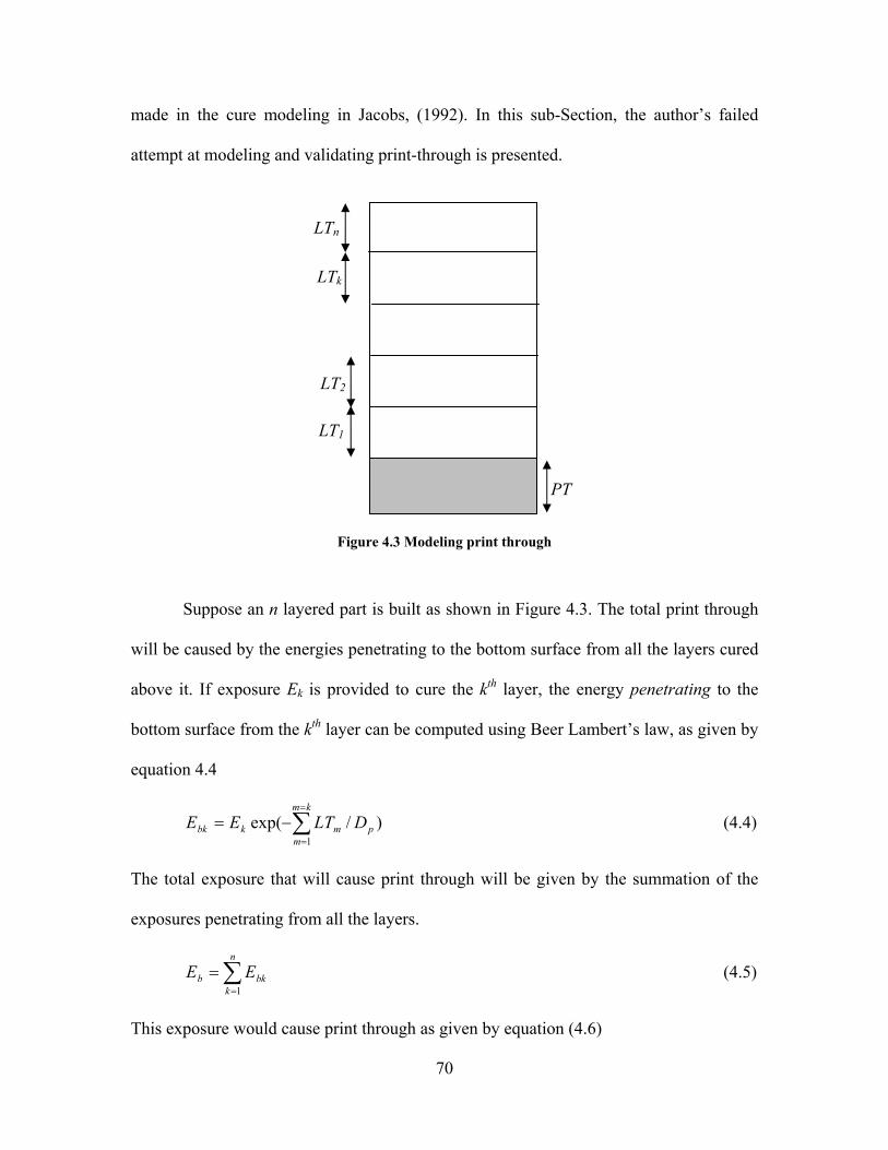
70
made in the cure modeling in Jacobs, (1992). In this sub-Section, the author’s failed
attempt at modeling and validating print-through is presented.
Figure 4.3 Modeling print through
Suppose an n layered part is built as shown in Figure 4.3. The total print through
will be caused by the energies penetrating to the bottom surface from all the layers cured
above it. If exposure Ek is provided to cure the kth layer, the energy penetrating to the
bottom surface from the kth layer can be computed using Beer Lambert’s law, as given by
equation 4.4
)/exp(1∑=
=
−=km
mpmkbk DLTEE (4.4)
The total exposure that will cause print through will be given by the summation of the
exposures penetrating from all the layers.
∑=
=n
kbkb EE
1 (4.5)
This exposure would cause print through as given by equation (4.6)
LTn
LTk
LT2
LT1
PT
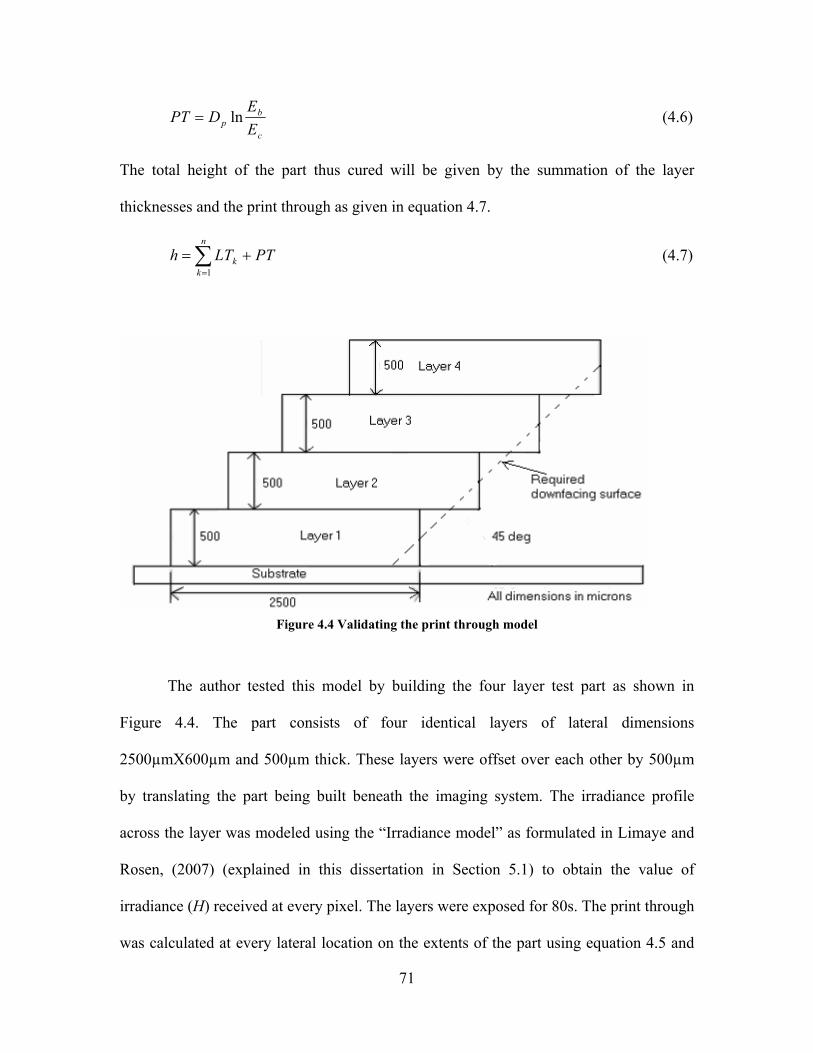
71
c
bp E
EDPT ln= (4.6)
The total height of the part thus cured will be given by the summation of the layer
thicknesses and the print through as given in equation 4.7.
PTLThn
kk += ∑
=1 (4.7)
Figure 4.4 Validating the print through model
The author tested this model by building the four layer test part as shown in
Figure 4.4. The part consists of four identical layers of lateral dimensions
2500µmX600µm and 500µm thick. These layers were offset over each other by 500µm
by translating the part being built beneath the imaging system. The irradiance profile
across the layer was modeled using the “Irradiance model” as formulated in Limaye and
Rosen, (2007) (explained in this dissertation in Section 5.1) to obtain the value of
irradiance (H) received at every pixel. The layers were exposed for 80s. The print through
was calculated at every lateral location on the extents of the part using equation 4.5 and
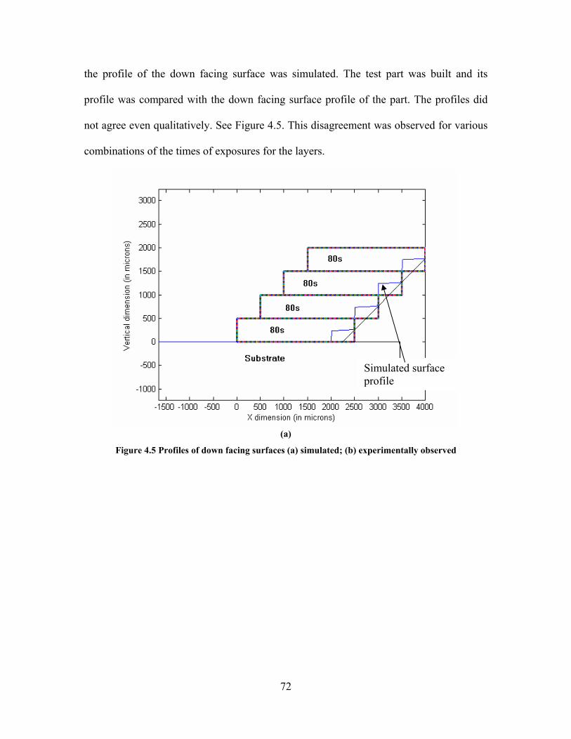
72
the profile of the down facing surface was simulated. The test part was built and its
profile was compared with the down facing surface profile of the part. The profiles did
not agree even qualitatively. See Figure 4.5. This disagreement was observed for various
combinations of the times of exposures for the layers.
(a)
Figure 4.5 Profiles of down facing surfaces (a) simulated; (b) experimentally observed
Simulated surface profile
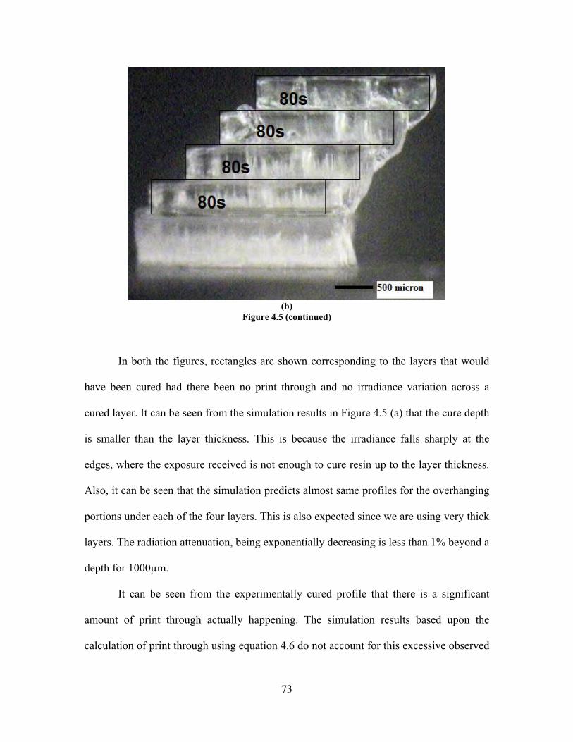
73
(b)
Figure 4.5 (continued)
In both the figures, rectangles are shown corresponding to the layers that would
have been cured had there been no print through and no irradiance variation across a
cured layer. It can be seen from the simulation results in Figure 4.5 (a) that the cure depth
is smaller than the layer thickness. This is because the irradiance falls sharply at the
edges, where the exposure received is not enough to cure resin up to the layer thickness.
Also, it can be seen that the simulation predicts almost same profiles for the overhanging
portions under each of the four layers. This is also expected since we are using very thick
layers. The radiation attenuation, being exponentially decreasing is less than 1% beyond a
depth for 1000µm.
It can be seen from the experimentally cured profile that there is a significant
amount of print through actually happening. The simulation results based upon the
calculation of print through using equation 4.6 do not account for this excessive observed

74
print through. This made the author questions some of the fundamental assumptions
made in the formulation of equation on 4.6. Two assumptions were identified as
explained in Section 4.2.2 and Section 4.2.3.
4.2.2 Modeling layer curing as a transient process
The print through model presented in equation 4.6 assumes that when any layer is
cured, all the energy supplied to cure the layer is supplied in an instant and the depth of
cure is proportional to the logarithm of exposure. Suppose that irradiance H is incident
on the resin surface for a duration t. It would supply an exposure tHE ⋅= . This energy
would get attenuated as it enters the resin, according to the Beer Lambert’s law. The
exposure at a depth z is given by )/exp( pz DzEE −= . Curing occurs at all points where
exposure is greater than or equal to Ec. The thickness of the layer cured will thus be given
by equation (4.8).
)/ln( cpd EtHDC ⋅= (4.8)
where Dp is the depth of penetration of the resin (a measure of attenuation of
radiation), and
Ec is the threshold exposure for polymerization.
This model assumes that the attenuation of radiation through a cured layer is the
same as that through uncured resin, given by the parameter Dp. This assumption is highly
suspicious, because most of the photo-initiator is consumed in cured resin. The chemical
composition of cured resin is significantly different from that of uncured resin, which will
definitely alter its rate of absorption of light. In other words, the depth of penetration for a
cured layer DpS is expected to be different from that of liquid resin DpL.
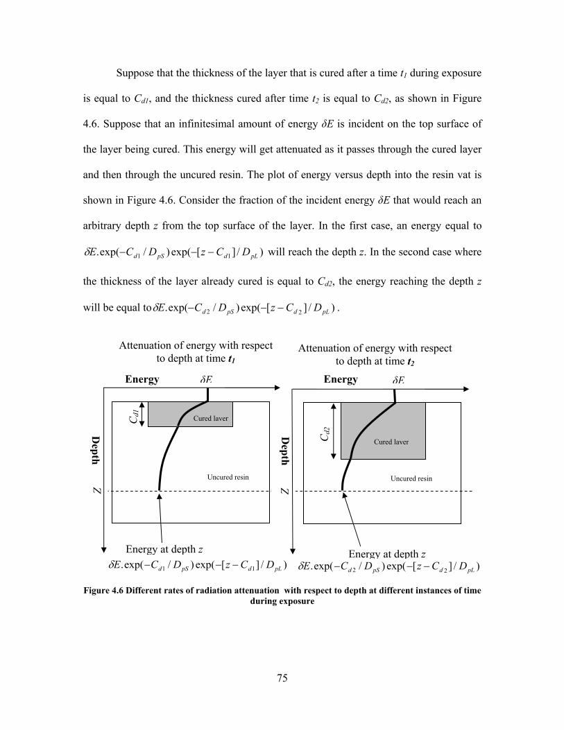
75
Suppose that the thickness of the layer that is cured after a time t1 during exposure
is equal to Cd1, and the thickness cured after time t2 is equal to Cd2, as shown in Figure
4.6. Suppose that an infinitesimal amount of energy δE is incident on the top surface of
the layer being cured. This energy will get attenuated as it passes through the cured layer
and then through the uncured resin. The plot of energy versus depth into the resin vat is
shown in Figure 4.6. Consider the fraction of the incident energy δE that would reach an
arbitrary depth z from the top surface of the layer. In the first case, an energy equal to
)/][exp()/exp(. 11 pLdpSd DCzDCE −−−δ will reach the depth z. In the second case where
the thickness of the layer already cured is equal to Cd2, the energy reaching the depth z
will be equal to )/][exp()/exp(. 22 pLdpSd DCzDCE −−−δ .
Figure 4.6 Different rates of radiation attenuation with respect to depth at different instances of time
during exposure
Z
Cd1
Cd2
Energy
Depth
δE
)/][exp()/exp(. 11 pLdpSd DCzDCE −−−δEnergy at depth z
Energy
Depth
δE
Energy at depth z )/][exp()/exp(. 22 pLdpSd DCzDCE −−−δ
Attenuation of energy with respect to depth at time t1
Attenuation of energy with respect to depth at time t2
Cured layer
Cured layer
Uncured resin Uncured resin
Z

76
Thus, the average attenuation of radiation per unit depth will vary with respect to
time. In other words, the rate of radiation attenuation with respect to depth, will vary with
respect to time. It is necessary to capture this effect of varying rate of attenuation on the
depth of cure. This leads us to Research Question 2a.
Research Question 2a: How to capture the effect of the varying rate of radiation
attenuation throughout the duration of exposure, as a layer gets cured?
Hypothesis: The effect of varying rate of attenuation as a layer gets cured can be
captured by modeling layer curing as a transient phenomenon, by discretizing the time
domain.
Explanation
Suppose the depth of penetration for a cured layer is DpS and that for the liquid
resin is DpL. By discretizing the time domain into infinitesimal time intervals (dt), we can
formulate a differential equation relating the incremental curing (dz) that would occur
during the time interval dt. By solving this differential equation, we can obtain a
relationship between the depth of cure and time of exposure.
By conducting experiments on our MPSLA system, we can see if we get the same
relationship between cure depth and exposure as that predicted by solving the differential
equation. This would validate our theory of the transient layer curing.
Task 1: Formulate the transient layer cure model
A differential equation relating the incremental curing dz and the infinitesimal
time interval dt shall be formulated and solved
Task 2: Validate the transient layer cure model

77
Layers shall be cured for various times of exposures and plotted against the
exposure supplied to cure them to validate the transient layer cure model
4.2.3 Quantifying effect of diffusion underneath cured layer
The print through model makes another assumption. It assumes that exposure is
additive (equation 4.5). In other words, it assumes that the total energy that would cause
print through is simply the algebraic summation of the energies that reach the bottom
surface from all the layers cured above it. The author finds this assumption highly invalid
for the MPSLA process. In case of the MPSLA process used by the author, a time
interval of up to one minute is allowed for the resin surface to level itself before any layer
is cured. The author expects that during this duration, reactive species underneath the
partially cured part would diffuse out into the vat and would carry energy away with
them. In addition, oxygen from the surrounding resin would diffuse towards the solid-
liquid interface and quench the excited species, thereby further reducing the amount of
energy carried by excited species at the bottom surface. These two diffusion phenomena
are expected to cause a fall in the net energy available at the bottom surface. The author
intended to pose his suspicion as Research Question 2b.
Research Question 2b: Is exposure at the bottom surface of a cured layer additive or
does it get significantly affected by diffusion of radicals and oxygen into the resin vat?
Hypothesis: The exposure is not additive because there is a significant diffusion of
radicals and oxygen in the resin vat.
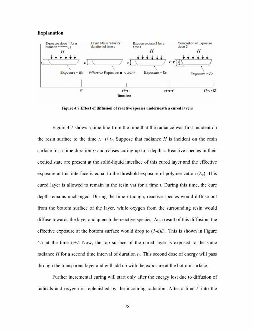
78
Explanation
Figure 4.7 Effect of diffusion of reactive species underneath a cured layers
Figure 4.7 shows a time line from the time that the radiance was first incident on
the resin surface to the time t1+t+t2. Suppose that radiance H is incident on the resin
surface for a time duration t1 and causes curing up to a depth z. Reactive species in their
excited state are present at the solid-liquid interface of this cured layer and the effective
exposure at this interface is equal to the threshold exposure of polymerization (Ec). This
cured layer is allowed to remain in the resin vat for a time t. During this time, the cure
depth remains unchanged. During the time t though, reactive species would diffuse out
from the bottom surface of the layer, while oxygen from the surrounding resin would
diffuse towards the layer and quench the reactive species. As a result of this diffusion, the
effective exposure at the bottom surface would drop to (1-k)Ec. This is shown in Figure
4.7 at the time t1+t. Now, the top surface of the cured layer is exposed to the same
radiance H for a second time interval of duration t2. This second dose of energy will pass
through the transparent layer and will add up with the exposure at the bottom surface.
Further incremental curing will start only after the energy lost due to diffusion of
radicals and oxygen is replenished by the incoming radiation. After a time t’ into the
H H H

79
second exposure dose, the lost energy will be replenished and the effective exposure at
the bottom surface will once again be equal to Ec. This is shown on the time line in
Figure 4.6 at the time t1+t+t’.
At the end of the second exposure dose of duration t2, the effective exposure at the
bottom surface will be as given in equation 4.9.
)/exp()()1( 2 pScb DztHEkE −⋅+−= (4.9)
This exposure is what will cause incremental curing upto a depth y as shown in Figure
4.7. The value of ‘k’ (let us call it as “Radical diffusion factor”) in equation (4.9) is
expected to be a strong function of time. We shall compute this factor experimentally.
Task 1: Validate the theory of diffusion of radicals
Single layered parts, as shown in Figure 4.7 shall be cured by supplying two
discrete exposure doses and by allowing different durations in between the two exposures
to allow time for the radicals and oxygen to diffuse. By measuring the thickness of the
layers cured, the value of the radical diffusion coefficient k shall be plotted and it shall be
seen if it is a logarithmic function of the time allowed for diffusion t (typical for
diffusion-based phenomena). If it is, then we can take a leap of faith to conclude that
radical diffusion occurs underneath a cured part.
4.2.4 Modeling print through and implementing Compensation zone approach
After having done the preceding work, the author again intends to pursue
modeling print through and hopes to get much better agreement between experimental
and analytical results. Using this model, it would be possible to simulate a down facing
surface and then, solve the print through equation to obtain the reduction in layer
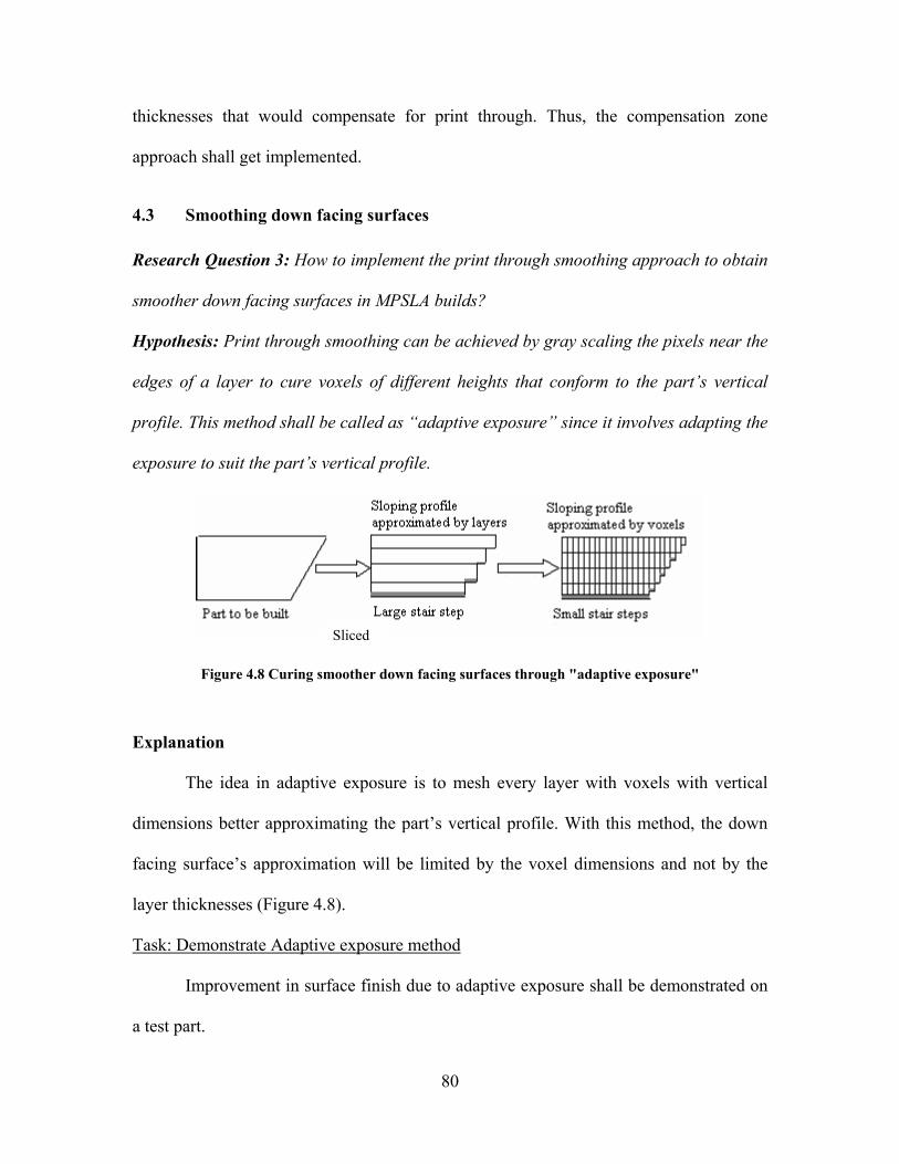
80
thicknesses that would compensate for print through. Thus, the compensation zone
approach shall get implemented.
4.3 Smoothing down facing surfaces
Research Question 3: How to implement the print through smoothing approach to obtain
smoother down facing surfaces in MPSLA builds?
Hypothesis: Print through smoothing can be achieved by gray scaling the pixels near the
edges of a layer to cure voxels of different heights that conform to the part’s vertical
profile. This method shall be called as “adaptive exposure” since it involves adapting the
exposure to suit the part’s vertical profile.
Figure 4.8 Curing smoother down facing surfaces through "adaptive exposure"
Explanation
The idea in adaptive exposure is to mesh every layer with voxels with vertical
dimensions better approximating the part’s vertical profile. With this method, the down
facing surface’s approximation will be limited by the voxel dimensions and not by the
layer thicknesses (Figure 4.8).
Task: Demonstrate Adaptive exposure method
Improvement in surface finish due to adaptive exposure shall be demonstrated on
a test part.
Sliced

81
4.4 Process planning for MPSLA
Suppose the part with quadratic up and down facing surfaces as shown in Figure
4.8 is to be built. There are requirements on the part’s lateral dimensions, vertical
dimensions, surface finish as well as build time. The curing of dimensionally accurate
parts has been addressed in Research Questions 2. Improvements to surface finish
through intelligent process planning have been addressed in Research Question 3. The
build time of an MPSLA part can be easily modeled by breaking down the part building
process into its constituent steps and summing the time required to complete each of
those steps.
Research Question 4: How to build a MPSLA part with multiple objectives of
dimensional accuracy, surface finish and build time?
Hypothesis: Process planning can be done in two steps. First, a multi-objective
optimization method, like the compromise DSP (Mistree et al., 1994) should be
formulated and solved to select the slicing scheme, i.e. layer thicknesses that would
obtain a tradeoff between the objectives of surface finish and build time. For this slicing
scheme, the compensation zone approach should be adopted to obtain part with accurate
vertical dimensions
Explanation
The layer thicknesses have the largest effect on two of our process objectives:
surface finish and build time. It can be intuitively seen that larger the number of layers,
greater would be the build time. Also, larger the number of layers to build a given a part,
smaller will be the layer thicknesses and thus, smoother would be the up facing surface.
Thus, a compromise DSP can be formulated and solved to generate slicing schemes that

82
would achieve tradeoffs between the goals of surface finish and build time. A set of
slicing schemes that are acceptable would be selected. The Compensation zone approach
shall be applied on each of these slicing schemes to reduce the print through errors.
Task: Formulate and test the multi objective process planning method
The following are the proposed steps of the process planning method.
1. Slice the CAD model and populate the slices with elements so that the surface
finish and build time requirements are satisfied as well as the lateral dimensional
requirements are satisfied.
2. Choose a couple of “likely to succeed” slicing schemes that would satisfy the
build time and surface finish requirements and pass them on to the second c-DSP.
3. Now, choose the combination of compensation zone thickness, and cure depths
that will give the required vertical dimension, i.e. satisfy equations 4.3, 4.4 and
4.5. The structure of the proposed process planning method is shown in Figure
4.8.

83
Figure 4.9 Multi objective process planning method
Summary
This chapter identifies the research questions that need to be addressed in order to
meet the research objective of formulating a process planning method for Mask
Projection Stereolithography. Research Question 1 deals with the modeling of image
formation in a computationally inexpensive manner. Research Question 2 deals with the
rigorous modeling and validation of the print through that occurs when multi-layered
parts are built. Research Question 3 deals with achieving print-through smoothing for
down facing surfaces, a phenomenon observed in laser scanning Stereolithography
systems, but never demonstrated in Mask Projection Stereolithography. Research
Multi-objective slicing algorithm
Compensation zone approach
List of bitmaps
List of time of exposures
Cusp height < 40µm
Build time < 30minutes

84
Question 4 deals with the formulation of a process planning method that will utilize all
the research done in answering research questions 1 to 3, in order to formulate a multi-
objective process planning method for Mask Projection Stereolithography.
85
CHAPTER 5 IRRADIANCE MODEL
In this chapter, Research Questions 1a and 1b, as presented in Chapter 4, are
tackled. In Section 5.1, the validity of the geometric optics approach to model the image
formation process for the MPSLA system is verified. In Section 5.2, the multi scale
modeling approach to model the irradiance distribution, is implemented and tested.
5.1 Geometric Optics to model image formation
Research Question 1 dealt with the approach to be used to model the image
formation process. The hypothesis was that geometric optics is a better approach than
physical optics to model the image formation process. This hypothesis is validated in this
section. In Section 5.1.1, the imaging system is modeled using the optical design software
OSLOTM to quantify the optical path difference (OPD) introduced due to aberrations.
This OPD is compared with the Rayleigh quarter wavelength criterion to show that the
system is ‘aberration limited’, as opposed to ‘diffraction limited’. In Section 5.1.2, the ray
tracing algorithm is used to model the dimensions of an image formed on the resin. These
dimensions are compared by curing a layer in the resin. This is used to quantify the
accuracy of the geometric optics approach for modeling image formation.
5.1.1 Quantifying the OPD
It has been observed that the imaging system of the realized MPSLA machine can
image an area comprising of 300x300 micromirrors or smaller with acceptable amounts
of distortions. Thus, the active area of the mask is only 300x300 pixels. The pitch of the
micro-mirrors (pixels) on the mask is 13.65µm. The maximum distance of any point on a
pattern displayed on the mask, from the optical axis, is 150 x 13.65 = 2047µm, i.e. 2.047
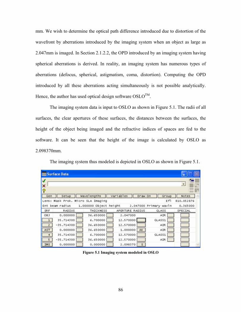
86
mm. We wish to determine the optical path difference introduced due to distortion of the
wavefront by aberrations introduced by the imaging system when an object as large as
2.047mm is imaged. In Section 2.1.2.2, the OPD introduced by an imaging system having
spherical aberrations is derived. In reality, an imaging system has numerous types of
aberrations (defocus, spherical, astigmatism, coma, distortion). Computing the OPD
introduced by all these aberrations acting simultaneously is not possible analytically.
Hence, the author has used optical design software OSLOTM.
The imaging system data is input to OSLO as shown in Figure 5.1. The radii of all
surfaces, the clear apertures of these surfaces, the distances between the surfaces, the
height of the object being imaged and the refractive indices of spaces are fed to the
software. It can be seen that the height of the image is calculated by OSLO as
2.098370mm.
The imaging system thus modeled is depicted in OSLO as shown in Figure 5.1.
Figure 5.1 Imaging system modeled in OSLO
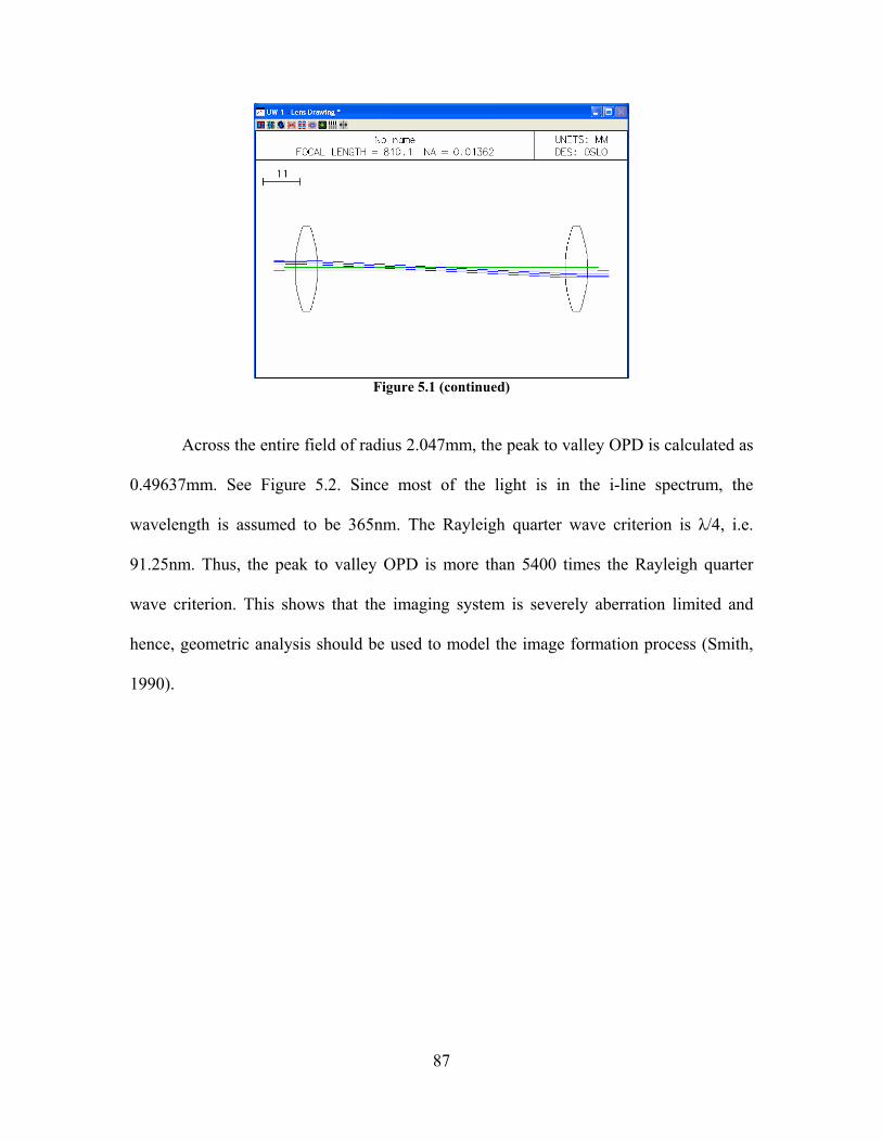
87
Figure 5.1 (continued)
Across the entire field of radius 2.047mm, the peak to valley OPD is calculated as
0.49637mm. See Figure 5.2. Since most of the light is in the i-line spectrum, the
wavelength is assumed to be 365nm. The Rayleigh quarter wave criterion is λ/4, i.e.
91.25nm. Thus, the peak to valley OPD is more than 5400 times the Rayleigh quarter
wave criterion. This shows that the imaging system is severely aberration limited and
hence, geometric analysis should be used to model the image formation process (Smith,
1990).

88
Figure 5.2 OPD calculated by OSLO
5.1.2 Irradiance model
Ray tracing is the method to model the irradiance across an image formed by an
aberration limited optical system. An exact ray tracing algorithm is formulated to trace
rays through the imaging system of the MPSLA system. The ray tracing equations
presented in Section 2.1.2.3, as presented in Smith, (1990), are used to formulate the ray
tracing algorithm.
The DMD is arranged so as to reflect a horizontal beam of light coming from the
collimating system downwards towards the imaging system. The orientation of a
displayed bitmap pattern in the three dimensional space and hence the co-ordinates of the
points from which rays shall be traced are computed before starting the ray tracing.
In the Figure 5.3(a), the starting orientation of the DMD chip is shown with its
plane perpendicular to the beam coming from the collimating system The global co-

89
ordinate system [XYZ] is defined as shown in the figure. X axis is the axis along the
beam coming from the collimating system, Z axis is vertically downwards and the Y axis
is perpendicular to the X and Z axes, along the plane of the DMD chip. The
micromirrors, in their neutral state, are parallel to the DMD chip as shown in Figure 5.3
(a). The co-ordinate system [XmYmZm] of one of the micromirrors on the DMD chip is
exactly aligned with the global co-ordinate system in the beginning as shown in Figure
5.3(a). The global co-ordinate system is centered at the midpoint of the chip. The local
co-ordinate system of every micro-mirror is centered at its midpoint. In the figure, the
origins of the global co-ordinate system and that of the micro-mirror being considered are
shown to be co-incident, but this is not necessary. In its ‘ON’ state, a mirror is tilted
about its diagonal by 100. The DMD needs to be oriented in such a sense, so that a micro-
mirror in its ‘ON’ state would reflect the horizontal beam coming from the collimating
system vertically downwards. Since the beam is coming along the global X axis, an ‘ON’
micro-mirror needs to be tilted at an angle 450 about the global Y axis. Since the micro-
mirror tilts about its diagonal, the diagonal needs to be aligned parallel to the global Y
axis. We align the DMD in such a way that this is achieved. The DMD chip is rotated
about the X axis by 450 to make the diagonal along which the micromirror would tilt,
parallel to the global Y axis. This is shown in Figure 5.3(b). Now, the DMD chip is
rotated by 550 about the global Y axis, so that when the micro-mirror tilts by 100 in its
‘ON’ state, it will be effectively tilted at 450 along the global Y axis and would thus
direct the beam vertically downwards

90
(a)
(b)
Figure 5.3 3D transformation of the DMD to reflect the light beam downwards
DMD chip
Micro mirror
Light beam from collimating system
Light beam from collimating system

91
.
When any bitmap is input to the Irradiance model, geometric transformations are
applied to the bitmap to account for the above mentioned alignment procedure. Then,
every ‘ON’ micro-mirror on the DMD is meshed with points and rays are traced from
each of these points to compute the irradiance distribution on the resin surface. This
procedure is explained in detail in Sections 5.1.2.1 to 5.1.2.3.
5.1.2.1 Geometric transformations to determine center of every ‘ON’ micromirror Given a bitmap, the ‘ON’ micro-mirrors on the DMD are identified. The co-
ordinates of the center of each micro-mirror is passed through the 3D transformations that
occur due to the alignment of the DMD as explained above. Suppose the global co-
ordinates of the center of a micro-mirror are given by (x1, y1, z1). It is passed through the
following transformations:
• Rotation about the X axis would change the co-ordinates to (x2, y2, z2)
12
112
112
)45cos()45sin()45sin()45cos(
xxyzyyzz
=+=−=
(5.1)
• Rotation about Y axis would change the co-ordinates to (x3, y3, z3)
23
223
223
)55cos()55sin()55sin()55cos(
yyxzx
xzz
=+−=+=
(5.2)
Since z2 = 0, equation (5.2) gets simplified as:
23
23
23
)55cos()55sin(
yyxxxz
===
(5.3)
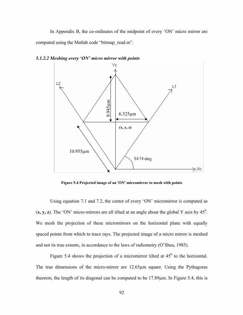
92
In Appendix B, the co-ordinates of the midpoint of every ‘ON’ micro mirror are
computed using the Matlab code “bitmap_read.m”.
5.1.2.2 Meshing every ‘ON’ micro mirror with points
Figure 5.4 Projected image of an 'ON' micromirror to mesh with points
Using equation 7.1 and 7.2, the center of every ‘ON’ micromirror is computed as
(x, y, z). The ‘ON’ micro-mirrors are all tilted at an angle about the global Y axis by 450.
We mesh the projection of these micromirrors on the horizontal plane with equally
spaced points from which to trace rays. The projected image of a micro mirror is meshed
and not its true extents, in accordance to the laws of radiometry (O’Shea, 1985).
Figure 5.4 shows the projection of a micromirror tilted at 450 to the horizontal.
The true dimensions of the micro-mirror are 12.65µm square. Using the Pythagoras
theorem, the length of its diagonal can be computed to be 17.89µm. In Figure 5.4, this is
(x, y, z)
10.955µm
6.325µm8.94
5µm

93
the dimension of the diagonal along the global Y axis. Due to the tilting by 450, the
shorter diagonal will be of length 17.89cos(450) = 12.65µm. From the dimensions of the
diagonals, it is possible to compute the side of the projected parallelogram in Figure 5.4,
using Pythagoras theorem, to be 10.955µm.
Consider a two dimensional co-ordinate system [XcYc] centered at the corner of
the projected micro mirror as shown in Figure 5.4. Consider another two dimensional co-
ordinate system [L1L2] centered at the same corner, with axes along the sides of the
projected image of the micro-mirror. The angle between the axes Xc and L1 is 54.740, as
can be found out using trigonometry.
The projected image of the micro-mirror is meshed by 121 points, by dividing
every side into 11 points. Given the location of a point in the [L1L2] co-ordinate system
as (a,b), we need to determine the co-ordinates of that point in [XcYc] co-ordinate system
and then, in global [X,Y] coordinate system. The transformations of the co-ordinates of a
point from the [L1L2] co-ordinate system to the global [XY] co-ordinate system is
achieved as follows.
Let l1 and l2 be unit vectors along the axes L1 and L2 respectively and xc and yc be
unit vectors along the Xc and Yc axes respectively. The relationship between these unit
vectors from different co-ordinate system can be obtained by projecting l1 and l2 on Xc
and Yc, as given in equation 5.4.
cc
cc
yxlyxl)74.54sin()74.54cos(
)74.54sin()74.54cos(
2
1
+−=+=
(5.4)
Any point with the co-ordinates (a,b) in the (L1,L2) co-ordinate system can be
expressed by the vector
21 blal + (5.5)
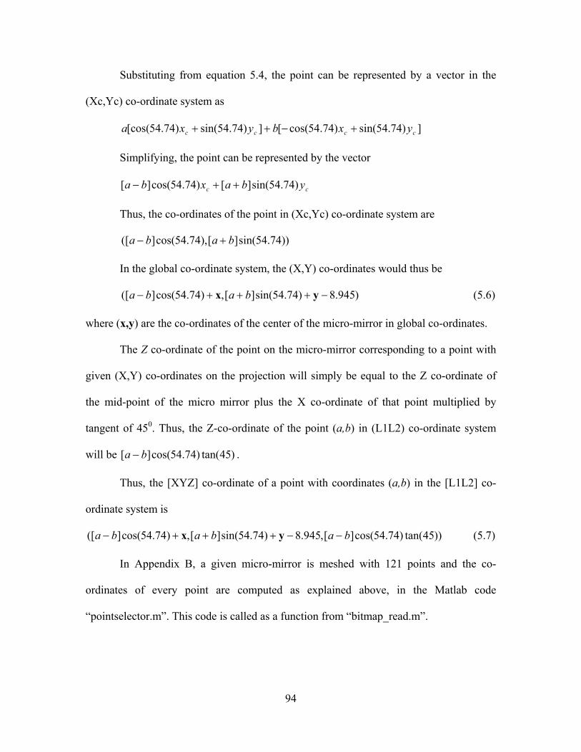
94
Substituting from equation 5.4, the point can be represented by a vector in the
(Xc,Yc) co-ordinate system as
])74.54sin()74.54cos([])74.54sin()74.54[cos( cccc yxbyxa +−++
Simplifying, the point can be represented by the vector
cc ybaxba )74.54sin(][)74.54cos(][ ++−
Thus, the co-ordinates of the point in (Xc,Yc) co-ordinate system are
))74.54sin(][),74.54cos(]([ baba +−
In the global co-ordinate system, the (X,Y) co-ordinates would thus be
)945.8)74.54sin(][,)74.54cos(]([ −+++− yx baba (5.6)
where (x,y) are the co-ordinates of the center of the micro-mirror in global co-ordinates.
The Z co-ordinate of the point on the micro-mirror corresponding to a point with
given (X,Y) co-ordinates on the projection will simply be equal to the Z co-ordinate of
the mid-point of the micro mirror plus the X co-ordinate of that point multiplied by
tangent of 450. Thus, the Z-co-ordinate of the point (a,b) in (L1L2) co-ordinate system
will be )45tan()74.54cos(][ ba − .
Thus, the [XYZ] co-ordinate of a point with coordinates (a,b) in the [L1L2] co-
ordinate system is
))45tan()74.54cos(][,945.8)74.54sin(][,)74.54cos(]([ bababa −−+++− yx (5.7)
In Appendix B, a given micro-mirror is meshed with 121 points and the co-
ordinates of every point are computed as explained above, in the Matlab code
“pointselector.m”. This code is called as a function from “bitmap_read.m”.
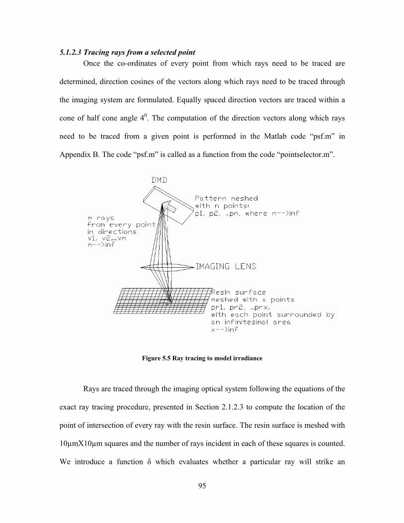
95
5.1.2.3 Tracing rays from a selected point Once the co-ordinates of every point from which rays need to be traced are
determined, direction cosines of the vectors along which rays need to be traced through
the imaging system are formulated. Equally spaced direction vectors are traced within a
cone of half cone angle 40. The computation of the direction vectors along which rays
need to be traced from a given point is performed in the Matlab code “psf.m” in
Appendix B. The code “psf.m” is called as a function from the code “pointselector.m”.
Figure 5.5 Ray tracing to model irradiance
Rays are traced through the imaging optical system following the equations of the
exact ray tracing procedure, presented in Section 2.1.2.3 to compute the location of the
point of intersection of every ray with the resin surface. The resin surface is meshed with
10µmX10µm squares and the number of rays incident in each of these squares is counted.
We introduce a function δ which evaluates whether a particular ray will strike an

96
infinitesimal area centered on a given point on the resin surface or not. Suppose that in
all, n points are used to mesh any bitmap displayed on the DMD and m rays are traced
from each of these n points as shown in Figure 5.5.
If a ray starting from point pj, along a direction vector vk intersects the resin surface in
one of the 10µmX10µm squares, centered on the point pri on the resin surface, then,
δ( pj, vk, pri ) = 1; else,
δ( pj, vk, pri ) = 0
The function δ is evaluated by adopting the exact ray tracing procedure as explained
in (Smith, 1990). In an exact ray trace the path of every ray is traced through the lens,
and the coordinates of the point where it intersects the image plane are analytically
computed. The imaging system parameters are used in the evaluation of the function
δ. The procedure of ray tracing has been explained in Section 2.1.2.3.
The irradiance received by any point on the resin surface will be proportional to the
number of rays striking an infinitesimal area centered on that point. The number of
rays striking a 10µmX10µm area centered at point pri on the resin surface will be
given by the function:
N pr p v pri j k ik
m
j
n
( ) ( , , )===∑∑ δ
11
(5.8)
Since the irradiance at a point on the resin surface is proportional to the number of
rays striking that point, the irradiance can be given by:
H pr c p v pri j k ik
m
j
n
( ) ( , , )===∑∑ δ
11
(5.9)

97
where c is a constant.
The constant c is calculated as follows:
Using a radiometer, the average irradiance across an aerial image can be measured.
Let the average irradiance be Hav. The average number of rays striking a point on the
resin surface will be given by (total number of rays/total number of points on the
resin surface) = nm/x. So, nm/x rays correspond to an irradiance of Hav. The constant
c is thus determined to be Hav/(nm/x). Substituting for c in the equation (6.3),
H pr H x nm p v pri av j k ik
m
j
n
( ) ( / ) ( , , )===∑∑ δ
11
(5.10)
Equation (5.10) will give accurate results when n ∞ and m ∞.
In equation 5.10, all rays are assumed to carry the same amount of energy. This is
because only a small portion of the center of the beam incident on the DMD is sampled
by the active area of the mask (300X300 pixel area). The power in this small area can be
assumed to be constant. Also, only a small portion at the center of the cone of rays
emitted from every point on every micro-mirror is allowed to pass through the telecentric
optic system. The power across this small cone (of less than 40 half cone angle), can also
be safely assumed to be constant.
While conducting the ray tracing, it is checked if the ray would passed through
the 2mm diameter aperture at the center of the telecentric imaging system. The tracing of
a ray from a given point on a given micro-mirror in a given direction is conducted by
means of the Matlab code “raytrace.m”. This code is called as a function from the Matlab
code “psf.m”. The code “raytrace.m” is also presented in Appendix B.

98
5.1.3 Validating Irradiance model
The bitmap in Figure 5.6 was run through the Irradiance model to generate the
irradiance distribution on the resin surface, the top view of which is shown in Figure 5.7.
The bitmap in Figure 5.6 was imaged onto the resin surface for a long duration of time
(160s) to cure single layer parts. For such a long duration of exposure, the entire
irradiated area would cure and the dimensions of the cured layer would be the same as the
dimensions of the irradiated area on the resin surface. One such cured layer in shown in
Figure 5.8.
Figure 5.6 Dimensions of the test bitmap imaged onto the resin surface

99
Figure 5.7 Irradiance profile on returned by the ray tracing code
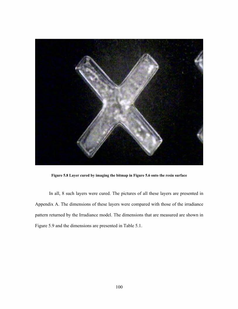
100
Figure 5.8 Layer cured by imaging the bitmap in Figure 5.6 onto the resin surface
In all, 8 such layers were cured. The pictures of all these layers are presented in
Appendix A. The dimensions of these layers were compared with those of the irradiance
pattern returned by the Irradiance model. The dimensions that are measured are shown in
Figure 5.9 and the dimensions are presented in Table 5.1.

101
Figure 5.9 Dimensions compared in Table 5.1
Table 5.1Comparison of experimental observed and analytically computed dimensions of the test layers
Test layers Dimension in µm p q r s t u
Layer #1 716.7 699.9 699.9 699.9 3899.6 3866.3 Layer #2 716.7 699.9 699.9 699.9 3899.6 3899.6 Layer #3 716.7 699.9 716.7 699.9 3899.6 3899.6 Layer #4 699.9 699.9 666.7 666.7 3866.3 3833.9 Layer #5 699.9 683.3 666.7 699.9 3866.3 3833.9 Layer #6 699.9 699.9 699.9 699.9 3866.3 3866.3 Layer #7 733.3 699.9 699.9 699.9 3899.6 3866.3 Layer #8 716.6 699.9 699.9 699.9 3866.3 3882.9 Average 712.5 697.8 693.7 695.7 3882.9 3868.6
Std. Deviation 11.82 5.87 17.64 11.74 17.8 25.5 Simulation 718.7 718.7 640.6 640.6 3718.7 3718.7
Error 6.2 20.9 -53.1 -55.1 -164.2 -149.9 % Error 0.86 2.91 -8.29 -8.6 -4.42 -4.03
p
qr
s
t u
102
It is clear from Table 5.1 that the image dimensions obtained by the ray tracing
algorithm very closely match the dimensions of the layer cured. Thus, the hypothesis that
geometric optics can be used to model the image formation by the MPSLA system is
validated. The errors observed in the dimensions are expected to have their origins in the
misalignment of the optical system and in the diffraction effects that have been ignored.
5.2 Multi scale Irradiance model
Consider the modeling the irradiance distribution obtained by running the test
bitmap as shown in Figure 5.6 through the ray tracing algorithm. In order to generate the
irradiance distribution, 2816 million rays were traced through the optical system. The
computation time was more than 152 hours. Research Question 2 dealt with reducing the
computation time of running the ray tracing approach for modeling image formation. A
multi-scale modeling method is proposed in Hypothesis 2 to speed up the computation of
irradiance distribution. According to this method, the irradiance is modeled at two scales:
pixel scale; and bitmap scale. At the pixel scale, a high resolution database documenting
the irradiance across the resin surface obtained when each micro-mirror is individually
imaged onto it, is populated by ray tracing. At the bitmap scale, this database is used to
compute the irradiance distribution across the resin surface when any bitmap is imaged
onto it. This approach is depicted in Figure 5.10.

103
Figure 5.10 Multi scale modeling of irradiance
There are two models formulated as a part of the Multi-scale Irradiance model: Pixel
Image model and Pixel Summation model.
Pixel Image model
As shown in Figure 5.10, the Pixel Image model is used to populate the “Pixel
Image database”. The Pixel Image model takes in the location of every micro-mirror on
the DMD individually as an input. The projection of this micromirror on the horizontal
plane is meshed with points and rays are traced from each of these points, following the
procedure as explained in Section 5.1.2. The irradiance distribution on the resin surface
obtained due to the imaging of this micro-mirror is recorded in the form of a matrix. A
6mmX6mm area on resin surface is meshed with 10µmX10µm squares. The irradiance
on the resin surface is thus recorded in the form of a 601X601 matrix. Thus, in general,
104
the irradiance from a micro-mirror with indices (p,q) is recorded in the Pixel Image
database as a 601X601 matrix Hpq.
In Appendix B, the Matlab code that implements the Pixel Image model to
populate the Pixel Image database is presented as “massive_database.m”. In order to
populate the database, the functions “pointselector.m”, “psf.m” and “raytrace.m”, as
documented in Appendix B and called by this code “massive.database.m”.
The population of the Pixel Image database entailed tracing of billions of rays.
The database populated is of size 7.65GBytes. It took around 500 hours to populate it.
Pixel Summation model
Given any bitmap, the co-ordinates of the ‘ON’ micro-mirrors on the DMD can be
obtained from the black pixels on bitmap. Given a set on ‘ON’ micro-mirrors, their
corresponding 601X601 matrices recording the irradiance on the resin surface can be
mined from the Pixel Image database. These matrices then are simply added to obtain the
irradiance distribution that would result when the bitmap is imaged onto the resin surface.
This is given by equation 5.11.
∑= pqHH (5.11)
where (p,q) are indices of all the ‘ON’ micro-mirrors on the DMD.
The Pixel Summation model (Equation 5.11) is implemented for the test bitmap
as shown in Figure 5.6, in the Matlab code “bitmap_read_database.m”, as presented in
Appendix B.
The test bitmap as shown in Figure 5.6 was passed through the Pixel Summation
model and the irradiance distribution across the resin surface was computed. This
irradiance distribution, as expected, was found to be exactly the same as that obtained by
105
running the same bitmap through the Irradiance model. The time required to generate this
irradiance distribution by using the Pixel Image database only 15 minutes. Thus, the
computation time has been reduced from 152 hours to 15 minutes by adopting this multi
scale modeling method.
5.3 Bitmap Generation method
The Multi scale Irradiance model can compute the lateral extents of the aerial
image that will be formed on the resin surface when a bitmap displayed on the DMD is
imaged onto it. The bitmap generation method uses the Pixel Image database to do just
the opposite, i.e., generate the bitmap to be displayed on the DMD in order to irradiate a
given area on the resin surface.
Using the Pixel Image database, the center of the pixel irradiated by every micro-
mirror is determined. A second database relating the location of the central element
irradiated by every micro-mirror on the DMD with the micro-mirror irradiating it is
created. This, we call as the “Element-Micromirror Mapping” database. Given the area to
be irradiated on the resin surface, it is meshed with 10µmX10µm elements, just like those
used in populating the Pixel Image database. Using the “Element Micromirror Mapping
database, every element composing the layer is checked to see if it is at the center of one
of the pixels irradiated by one of the micro-mirrors. If it is, then that micro-mirror is
deemed as ‘ON’. Knowing the micro mirrors that are ‘ON’, it is possible to generate the
bitmap with a black pixel corresponding to every ‘ON’ micro mirror and a white pixel
corresponding to every ‘OFF’ micro mirror. The Inverse Irradiance model is in the form
of a computer code which accomplishes the above mentioned tasks.
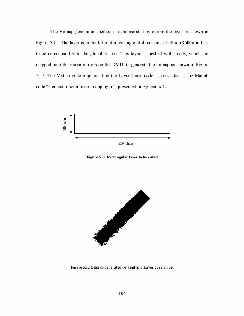
106
The Bitmap generation method is demonstrated by curing the layer as shown in
Figure 5.11. The layer is in the form of a rectangle of dimensions 2500µmX600µm. It is
to be cured parallel to the global X axis. This layer is meshed with pixels, which are
mapped onto the micro-mirrors on the DMD, to generate the bitmap as shown in Figure
5.12. The Matlab code implementing the Layer Cure model is presented as the Matlab
code “element_micromirror_mapping.m”, presented in Appendix C.
Figure 5.11 Rectangular layer to be cured
Figure 5.12 Bitmap generated by applying Layer cure model
2500µm
600µ
m

107
The bitmap in Figure 5.12 can be seen to be getting blurry towards the part
corresponding to the global negative Z axis. This blurriness is related to the mapping of
elements on the resin surface with the micro-mirrors and also with the focusing errors.
Due to the tilted mounting of the DMD, the object distances change along the Z axis.
There are focusing errors towards the negative Z axis, and the shapes of the pixels
irradiated by micro-mirrors in that region are irregular in shape. This causes errors and
approximations in the determination of the central element irradiated by micro-mirrors
that are located towards the negative Z direction. When the elements on the layer are
mapped onto the micro-mirrors, some of the micro-mirrors are not identified as ‘ON’
because their approximated center of the irradiated pixel is not a part of the layer.
Hence, a manual step is performed, in which the ‘OFF’ micro-mirrors
(corresponding to white pixels) dotting in between the ‘ON’ micro-mirrors (black pixels)
are manually turned on (i.e. pixels are turned black.). This smoothing of the bitmap is
performed to obtain the bitmap presented in Figure 5.13.
Figure 5.13 Bitmap generated by the pixel mapping database manually smoothened

108
Note that the smoothing out is done manually by the author by exercising his own
judgment. A better filtering or an edge detection algorithm should be implemented in
future to do the smoothing.
The smoothened bitmap was imaged onto the resin surface to cure three layers, as
shown in Figure 5.13. The lengths and widths of each of these layers were measured to be
2433µm and 566.67µm respectively. This good agreement between the required and the
obtained dimensions of the rectangular layer demonstrates the Inverse Irradiance model
and also further bolsters the Irradiance model itself.
Figure 5.14 Rectangular layers cured by imaging bitmap in Figure 5.13 onto the resin surface
109
Summary
In this chapter, the modeling of irradiance that would be supplied to the resin
surface when a given bitmap is imaged onto it is modeled. The geometric theory of optics
is shown to be valid for the modeling of image formation in case of an aberration limited
system such as the author’s. A ray tracing algorithm is formulated to model the image
formation process. Test layers have been cured on the MPSLA part and the ray tracing
algorithm has been shown to be valid within 8.6% error.
A multi scale modeling approach, which allows the computationally intensive
task of computing image formation through ray tracing manageable is also presented.
The chapter ends with the Bitmap Generation model, which generates the bitmap
to be displayed on the DMD in order to irradiate a given area on the resin surface.
Progress made towards answering research questions
In this chapter, research questions 1(a) and 1(b) are answered. Research question
1(a) dealt with choosing the optical theory to model image formation by the MPSLA
system. There are two theories for modeling image formation: geometric optics and
physical optics. In this chapter, the Optical Path Difference (OPD) of the telecentric
imaging system of the MPSLA system designed as a part of this research (Chapter 3) is
quantified. The OPD is shown to be more than 4000 times the Rayleigh limit (λ/4), and
thus the imaging system is shown to be aberration limited. The image formation for
aberration limited systems is modeled using the theory of geometric optics. A ray tracing
algorithm is formulated in this chapter to formulate the “Irradiance model”. The
Irradiance model computes the irradiance on the resin surface when a given bitmap is

110
imaged onto it. The model is validated by curing test layers on the MPSLA system and
comparing the dimensions of these layers with those of the irradiate area computed by
using the Irradiance model.
Research question 1(b) was concerning reducing the computation time involved in
implementing a ray tracing algorithm, which entails tracing of billions of rays through the
imaging system. A multi scale modeling strategy has been presented in this chapter to
reduce the computational expense of executing Irradiance model. “Pixel image model” is
formulated that traces rays from each micro mirror on the DMD individually and
computes the irradiance on the resin surface when that particular micro mirror is imaged
onto it. A “Pixel image database” which stores the irradiance across the pixels irradiated
by all the micro-mirrors on the DMD is populated. Once this database is formulated, the
image modeling can be done very rapidly. Give a bitmap to be imaged onto the resin
surface, the ‘ON’ pixels of the bitmap are identified, the corresponding pixels are mined
from the Pixel image database and are overlapped to obtain the irradiance on the resin
surface. The improvement in computational efficiency is demonstrated in this chapter by
modeling the image formation of a test bitmap without using the multi scale modeling
approach and using the multi scale modeling approach. The reduction in computation
time was found to be from 114 hours to 15 minutes.

111
CHAPTER 6 BUILDING ACCURATE THREE DIMENSIONAL PARTS
In Chapter 5, the Irradiance model was formulated which computes the irradiance
received by the resin surface when a bitmap is imaged onto it. This enables curing of
dimensionally accurate layers. In this chapter, the print through errors that would result
when layers are cured over each other are modeled. Research Question 2 deals with
avoiding the print through errors by adopting the “compensation zone” approach.
Research Question 2 has been broken down into two sub research questions, questioning
long held assumptions about the curing process of Stereolithography resins. The
hypotheses presented for these research questions are tested in this chapter.
In Section 6.1, the transient model of layer curing is formulated and validated.
This model takes into account the changing rate of attenuation of light in resin during
exposure. In Section 6.2, the effect of diffusion of reactive species and oxygen molecules
underneath a part being built, on the print through, is modeled and validated. In Section
6.3, the models formulated in Sections 6.1 and 6.2 are utilized to model the print through
that would occur when multiple layers are built over each other. The down facing surface
profile of the four-layered part presented in Figure 4.4 is simulated and validated in
Section 6.4. In Section 6.5, the compensation zone approach is implemented, utilizing the
derivations made in Sections 6.3 and 6.4, to compute the process parameters that would
build the required test part with accurate down-facing surface.
Research Question 3 was regarding employing the compensation zone approach
to smoothen the down facing surfaces of MPSLA builds. In Section 6.6, an
implementation of the compensation zone approach to smoothen the down facing
surfaces of MPSLA builds is demonstrated.

112
6.1 Transient layer cure model
The cure model presented in standard Stereolithography texts, like Jacobs (1992),
is fairly simple. It assumes that the depth of cure is proportional to the logarithm of
exposure and assumes the threshold model of resin cure. Suppose that irradiance H is
incident on the resin surface for a duration t. It would supply an exposure tHE ⋅= . This
energy would get attenuated as it enters the resin, according to the Beer Lambert’s law.
The exposure at a depth z is given by )/exp( pz DzEE −= . Curing occurs at all points
where exposure is greater than or equal to Ec. The thickness of the layer cured will thus
be given by equation (6.1).
)/ln( cpd EtHDC ⋅= (6.1)
where Dp is the depth of penetration of the resin (a measure of attenuation of
radiation), and
Ec is the threshold exposure for polymerization.
This model assumes that the attenuation of radiation through a cured layer is the
same as that through uncured resin, given by the parameter Dp. The author has observed
experimentally that the rate of radiation attenuation through a cured layer is significantly
less than that through liquid resin. Thus, the depth of penetration for a cured layer DpS is
expected to be different from that for the liquid resin DpL. The effect of these different
rates of attenuation on the cure depth is captured in this section by modeling layer curing
as a transient phenomenon.
Suppose irradiation H is incident on the resin surface at a particular location. It
will initiate curing after time tc (let us call it as “critical time”), when the exposure
received by the resin equals Ec.
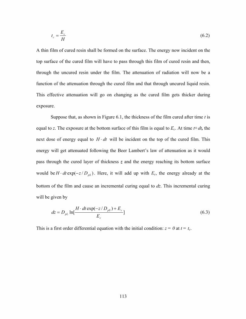
113
HE
t cc = (6.2)
A thin film of cured resin shall be formed on the surface. The energy now incident on the
top surface of the cured film will have to pass through this film of cured resin and then,
through the uncured resin under the film. The attenuation of radiation will now be a
function of the attenuation through the cured film and that through uncured liquid resin.
This effective attenuation will go on changing as the cured film gets thicker during
exposure.
Suppose that, as shown in Figure 6.1, the thickness of the film cured after time t is
equal to z. The exposure at the bottom surface of this film is equal to Ec. At time t+dt, the
next dose of energy equal to dtH ⋅ will be incident on the top of the cured film. This
energy will get attenuated following the Beer Lambert’s law of attenuation as it would
pass through the cured layer of thickness z and the energy reaching its bottom surface
would be )/exp( pSDzdtH −⋅ . Here, it will add up with Ec, the energy already at the
bottom of the film and cause an incremental curing equal to dz. This incremental curing
will be given by
])/exp(
ln[c
cpSpL E
EDzdtHDdz
+−⋅= (6.3)
This is a first order differential equation with the initial condition: z = 0 at t = tc.

114
Figure 6.1 Modeling layer curing as a transient phenomenon
Equation 6.3 was solved numerically to obtain the relationship between the depth
of cure (z) and the time of exposure (t). The solution to equation 6.3 converged when the
time domain was discretized to dt = 0.1s. In equation 6.3, the parameters DpL, DpS and Ec
are to be determined experimentally.
Characterizing the resin
In order to determine these parameters, the experimental procedure as shown in
Figure 6.2 was adopted. An optical window was placed in contact with the free surface of
resin contained in a vat and lines were imaged onto the resin surface for various time
durations. Curing was first noticed at 15s. The time durations were incremented in steps
of 5s, from 15s to 50s. This range of the times of exposure is fairly close to the typical
times of exposure for the author’s MPSLA system. Three lines were cured for each time
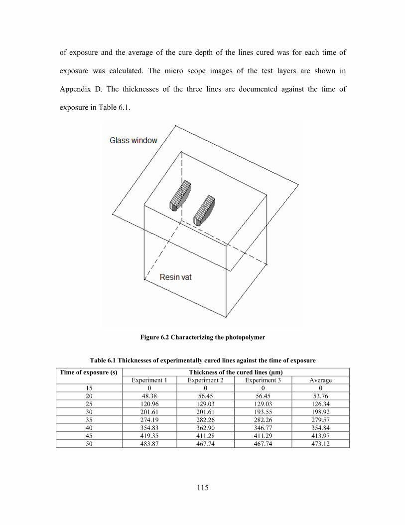
115
of exposure and the average of the cure depth of the lines cured was for each time of
exposure was calculated. The micro scope images of the test layers are shown in
Appendix D. The thicknesses of the three lines are documented against the time of
exposure in Table 6.1.
Figure 6.2 Characterizing the photopolymer
Table 6.1 Thicknesses of experimentally cured lines against the time of exposure
Thickness of the cured lines (µm) Time of exposure (s) Experiment 1 Experiment 2 Experiment 3 Average
15 0 0 0 0 20 48.38 56.45 56.45 53.76 25 120.96 129.03 129.03 126.34 30 201.61 201.61 193.55 198.92 35 274.19 282.26 282.26 279.57 40 354.83 362.90 346.77 354.84 45 419.35 411.28 411.29 413.97 50 483.87 467.74 467.74 473.12

116
The plot of the average cure depth of the line cured versus the time of exposure
was found to be linear, as shown in Figure 6.3. Hadipoespito et al, (2003) have
characterized the same photopolymer (DSM SOMOS 10120) using their Mask Projection
Stereolithography system and have also observed a linear relationship between cure depth
and time of exposure. The linear relationship between cure depth and time of exposure
cannot be explained by the standard SLA theory which assumes equal rates of radiation
attenuation through cured and uncured resin.
Equation 6.3 was integrated numerically, by discretizing the time domain into
durations of 0.1s. The analytical and experimental results agreed the best when the values
of the unknown parameters were chosen to be:
DpL = 0.192mm
DpS infinity
Ec = 10.2 mJ/cm2
From Table 6.2, it can be seen that the experimental and analytical values of cure
depths agree very well. The value of the depth of penetration through liquid resin (Dp)
and that of the threshold exposure of polymerization (Ec) are specified by the
manufacturer to be 0.16mm and 9.81mJ/cm2 respectively. These values agree very
closely with the values that have been measured. It should be noted that the value of
depth of penetration through cured resin (DpS) tends to infinity, indicating that a cured
layer is almost transparent to radiation.
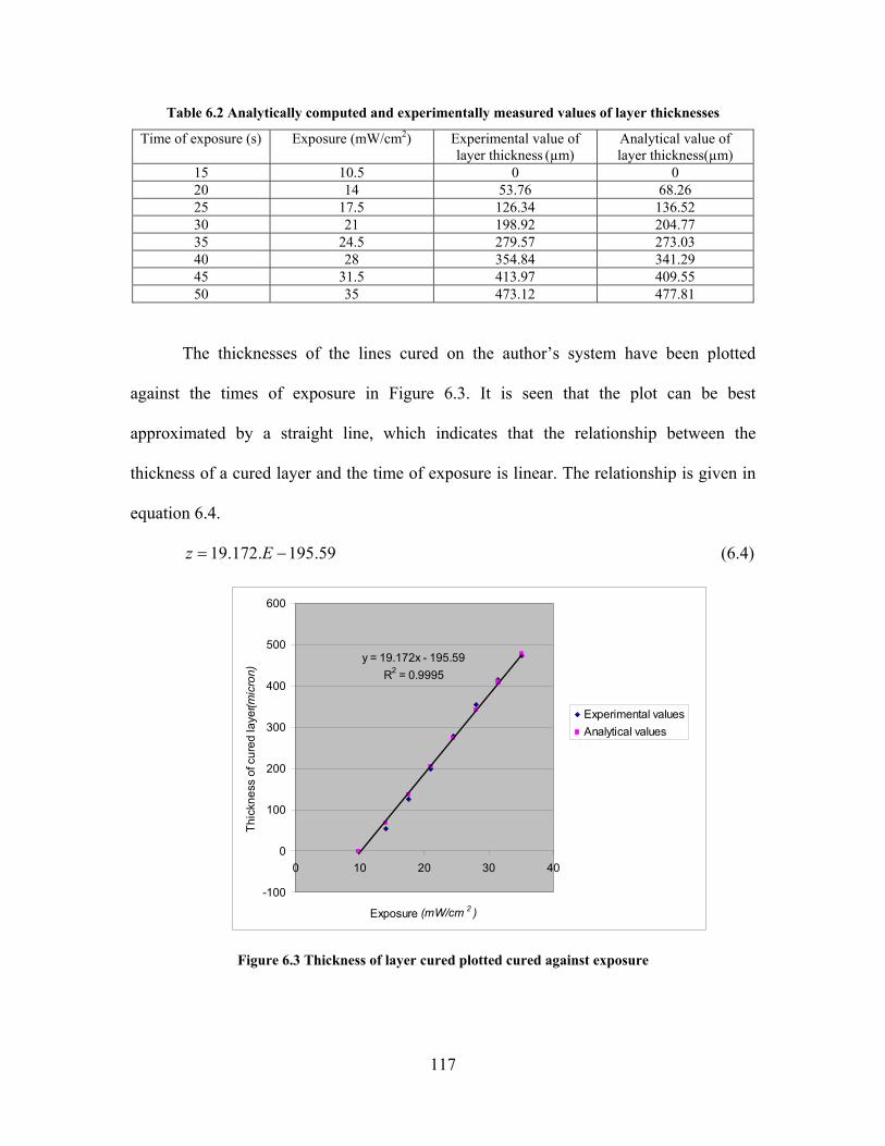
117
Table 6.2 Analytically computed and experimentally measured values of layer thicknesses
Time of exposure (s) Exposure (mW/cm2) Experimental value of layer thickness (µm)
Analytical value of layer thickness(µm)
15 10.5 0 0 20 14 53.76 68.26 25 17.5 126.34 136.52 30 21 198.92 204.77 35 24.5 279.57 273.03 40 28 354.84 341.29 45 31.5 413.97 409.55 50 35 473.12 477.81
The thicknesses of the lines cured on the author’s system have been plotted
against the times of exposure in Figure 6.3. It is seen that the plot can be best
approximated by a straight line, which indicates that the relationship between the
thickness of a cured layer and the time of exposure is linear. The relationship is given in
equation 6.4.
59.195.172.19 −= Ez (6.4)
Figure 6.3 Thickness of layer cured plotted cured against exposure
y = 19.172x - 195.59R2 = 0.9995
-100
0
100
200
300
400
500
600
0 10 20 30 40
Exposure (mW/cm 2 )
Thic
knes
s of
cur
ed la
yer (micron)
Experimental valuesAnalytical values

118
In general, the author postulates that the working curve for a Stereolithography
resin used with a Mask Projection Stereolithography system is linear, of the form
)( cpM EEDz −⋅= (6.5)
where DpM is the effective slope of the working curve, which is the rate at which
the cure-front propagates into the resin depth; and
Ec is the threshold exposure of polymerization.
For the MPSLA system under consideration,
DpM = 19.172 µm/(mW/cm2), or 1.9172mm3/mW and
Ec = 10.2 mW/cm2
It should be noted that linear relationship between cured depth and time of
exposure will be observed only for those resins for which the rate of radiation attenuation
through cured resin is negligible compared to that through uncured resin.
6.2 Effect of diffusion of radicals and oxygen
Jacobs, (1992) assumes exposure to be additive. This assumption means that if a
particular location in the depth of resin receives multiple doses of exposures, their effect
is the same as if the combined exposure was continuous. The author has experimentally
found that the additive nature of exposure is a strong function of time.
Suppose that, irradiance H is incident on the resin surface for a time duration t1
and causes curing up to a depth z. This is plotted in Figure 6.4. This cured layer is
allowed to remain in the resin bath for a time t. Now, the top surface of the cured layer is
supplied the radiance H for a second time interval of duration t2. This second dose of
energy will pass through the transparent layer and will add up with the exposure at the
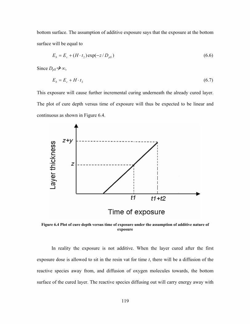
119
bottom surface. The assumption of additive exposure says that the exposure at the bottom
surface will be equal to
)/exp()( 2 pScb DztHEE −⋅+= (6.6)
Since DpS ∞,
2tHEE cb ⋅+= (6.7)
This exposure will cause further incremental curing underneath the already cured layer.
The plot of cure depth versus time of exposure will thus be expected to be linear and
continuous as shown in Figure 6.4.
Figure 6.4 Plot of cure depth versus time of exposure under the assumption of additive nature of
exposure
In reality the exposure is not additive. When the layer cured after the first
exposure dose is allowed to sit in the resin vat for time t, there will be a diffusion of the
reactive species away from, and diffusion of oxygen molecules towards, the bottom
surface of the cured layer. The reactive species diffusing out will carry energy away with
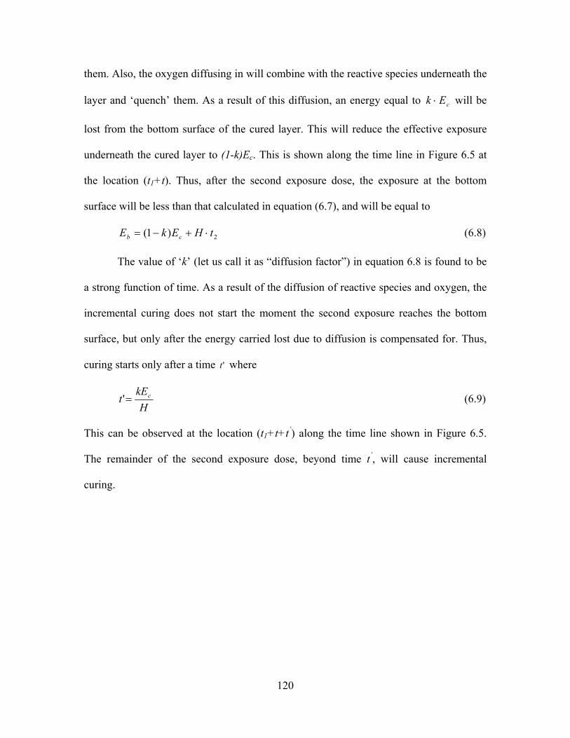
120
them. Also, the oxygen diffusing in will combine with the reactive species underneath the
layer and ‘quench’ them. As a result of this diffusion, an energy equal to cEk ⋅ will be
lost from the bottom surface of the cured layer. This will reduce the effective exposure
underneath the cured layer to (1-k)Ec. This is shown along the time line in Figure 6.5 at
the location (t1+t). Thus, after the second exposure dose, the exposure at the bottom
surface will be less than that calculated in equation (6.7), and will be equal to
2)1( tHEkE cb ⋅+−= (6.8)
The value of ‘k’ (let us call it as “diffusion factor”) in equation 6.8 is found to be
a strong function of time. As a result of the diffusion of reactive species and oxygen, the
incremental curing does not start the moment the second exposure reaches the bottom
surface, but only after the energy carried lost due to diffusion is compensated for. Thus,
curing starts only after a time 't where
HkE
t c=' (6.9)
This can be observed at the location (t1+t+t’) along the time line shown in Figure 6.5.
The remainder of the second exposure dose, beyond time t’, will cause incremental
curing.
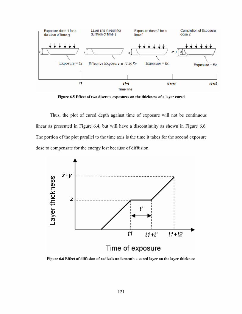
121
Figure 6.5 Effect of two discrete exposures on the thickness of a layer cured
Thus, the plot of cured depth against time of exposure will not be continuous
linear as presented in Figure 6.4, but will have a discontinuity as shown in Figure 6.6.
The portion of the plot parallel to the time axis is the time it takes for the second exposure
dose to compensate for the energy lost because of diffusion.
Figure 6.6 Effect of diffusion of radicals underneath a cured layer on the layer thickness

122
Measuring the value of k
The value of diffusion factor ‘k’ is measured experimentally as follows. The same
experimental arrangement as shown in Figure 6.2 is used, with a glass window kept flush
with the free surface of resin held in a vat. A single layer is cured sticking to the glass, for
by imaging a line onto the resin for 25s. This layer is allowed to remain in the vat for a
variable duration of time, called ‘waiting time’, (t seconds) and then, the same line is
again imaged onto the resin surface for 25s. The cure depth of the line cured after this
two exposure dose was measured. The micro scope images of the test layers are presented
in Appendix E. In all three replicate experiments were conducted for each duration of
‘waiting time’. The final thicknesses of the lines cured after the two exposure doses are
tabulated against the waiting time in Table 6.3.
Table 6.3 Thicknesses of lines cured with two discrete exposure doses
Thickness of the line cured after two exposure doses (µm) Waiting time between exposures (s) Experiment 1 Experiment 2 Experiment 3 Average
4 467.7 483.9 - 475.8 30 375 388.9 368.1 377.3 60 333.3 347.2 340.3 340.3 120 312.5 305.6 305.6 307.9 180 298.6 291.7 263.9 284.7
The value of t' which gave the best agreement with the depths of the cured line
was obtained experimentally. The plots are shown in Figure 6.7.
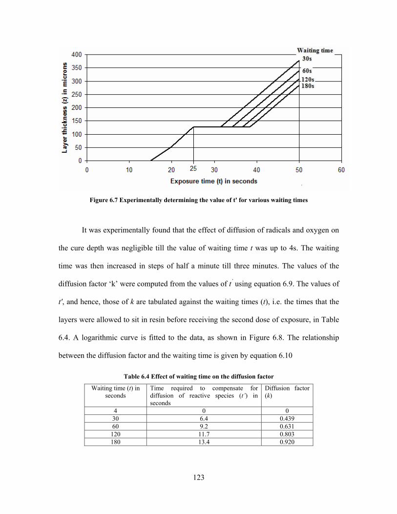
123
Figure 6.7 Experimentally determining the value of t' for various waiting times
It was experimentally found that the effect of diffusion of radicals and oxygen on
the cure depth was negligible till the value of waiting time t was up to 4s. The waiting
time was then increased in steps of half a minute till three minutes. The values of the
diffusion factor ‘k’ were computed from the values of t’ using equation 6.9. The values of
t', and hence, those of k are tabulated against the waiting times (t), i.e. the times that the
layers were allowed to sit in resin before receiving the second dose of exposure, in Table
6.4. A logarithmic curve is fitted to the data, as shown in Figure 6.8. The relationship
between the diffusion factor and the waiting time is given by equation 6.10
Table 6.4 Effect of waiting time on the diffusion factor
Waiting time (t) in seconds
Time required to compensate for diffusion of reactive species (t’) in seconds
Diffusion factor (k)
4 0 0 30 6.4 0.439 60 9.2 0.631
120 11.7 0.803 180 13.4 0.920

124
y = 0.2406Ln(x) - 0.3491R2 = 0.9971
-0.200
0.000
0.200
0.400
0.600
0.800
1.000
0 50 100 150 200
Waiting time (t) in seconds
Radi
cal d
iffus
ion
coef
ficie
nt (k
)
Figure 6.8 Plot of the radical diffusion factor against the waiting time
3491.0)ln(2406.0 −= tk (6.10)
The general form of equation relating the diffusion factor and time allowed for
diffusion is
CtBk −= )ln( (6.11)
where B and C are constants that will depend upon the resin, the temperature of
resin and even the size of the vat.
Thus, the energy at a cure front, i.e. at solid-liquid interface sitting in a resin vat
for t seconds will be given by
ct
ct
EtBCEEkE
⋅−+=−=
)]ln(1[)1(
(6.12)
6.3 Modeling print through
Based on the transient layer cure model and the diffusion model developed in
Sections 6.1 and 6.2, it is possible to model the print-through that would occur when a
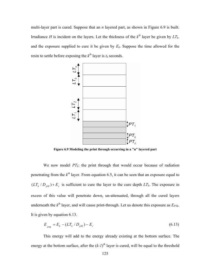
125
multi-layer part is cured. Suppose that an n layered part, as shown in Figure 6.9 is built.
Irradiance H is incident on the layers. Let the thickness of the kth layer be given by LTk.
and the exposure supplied to cure it be given by Ek. Suppose the time allowed for the
resin to settle before exposing the kth layer is tk seconds.
Figure 6.9 Modeling the print through occurring in a "n" layered part
We now model PTk: the print through that would occur because of radiation
penetrating from the kth layer. From equation 6.5, it can be seen that an exposure equal to
cpMk EDLT +)/( is sufficient to cure the layer to the cure depth LTk. The exposure in
excess of this value will penetrate down, un-attenuated, through all the cured layers
underneath the kth layer, and will cause print-through. Let us denote this exposure as EPTk.
It is given by equation 6.13.
cpMkkPTkEDLTEE −−= )/( (6.13)
This energy will add to the energy already existing at the bottom surface. The
energy at the bottom surface, after the (k-1)th layer is cured, will be equal to the threshold

126
exposure of polymerization Ec. The diffusion of radicals would have occurred at the
bottom surface for a time tdk, given as the summation of the time that was allowed for the
resin to settle before exposing the kth layer, and the time that it took for the kth layer to be
cured.
tdk = tk + [(LTk /DpM) + Ec]/H (6.14)
After the diffusion of reactive species and oxygen that would occur during the
time tdk, we can compute the effective exposure at the bottom surface of the part being
cured by applying equation (6.12).
cdkb EtBCE )]ln(1[ −+= (6.15)
The print-through will be caused by exposure Ebk at the bottom surface, given as the
addition of the exposures given by equations 6.13 and 6.15.
ckdcpMkkbk EtBCEDLTEE )]ln(1[)/( −++−−= (6.16)
Simplifying,
cdkpMkkbk EtBCDLTEE )]ln([)/( −+−= (6.17)
The print through caused by this exposure can be easily derived from equation 6.5 as
)( cbkpMk EEDPT −= (6.18)
}]1)ln([)/({ cdkpMkkpMk EtBCDLTEDPT −−+−= (6.19)
The total print through will be equal to
∑==
n
kkPTPT
1 (6.20)
The total height of the part cured will thereby be equal to
∑ ∑+== =
n
k
n
kkk PTLTh
1 1 (6.21)
127
Simplifying equation 6.21 by plugging in the value of print through from equation 6.19,
we get
]}]1)ln([)/({[11∑∑==
−−+−+=n
kcdkpMkkpM
n
kk EtBCDLTEDLTh (6.22)
where
Ek = ktH ⋅ (tk being the time of imaging)
tdk = tk + [(LTk /DpM ) + Ec]/H
pMD = 1.9172mm3/mW
B = 0.2406
C = 0.3491
Ec = 10.2 mJ/cm2
Effect of layer thickness on the height of the pixel column
Equation 6.22 can be further simplified as
∑ ∑∑
∑∑
= ==
==
−−−++=
−−−++=
n
k
n
lkcdkkpM
n
kk
n
kkcdkkpM
n
kk
LTEtBCEDLTh
LTEtBCEDLTh
1 11
11
}]1)ln([{
]}]1)ln([{[
∑=
−−+=n
kcdkkpM EtBCEDh
1}]1)ln([{ (6.23)
It would appear from equation 6.23 that there is no terms LTk in the equation that
gives the height of the pixel column and hence, might indicate that the height of a pixel
column that will be cured is independent of the layer thicknesses. However, the reader
must note that the variable tdk in equation 6.23, which is the time allowed for diffusion of
reactive species and oxygen molecules is dependent upon the layer thicknesses.

128
Also, the minimum limit on the exposure Ek incident on the kth layer is dependent
upon the thickness of the kth layer, i.e. LTk. Thus, the values of the layer thicknesses will
influence equation 6.23 even though no LTk terms appear in it. The layer thickness will
decide the time allowed for diffusion (tdk) before the kth layer is imaged and the limit on
exposure (Ek) supplied to cure the kth layer.
6.4 Simulating down facing profile of a test part
In this section, the print through model developed in Section 6.3 is used to
simulate a test part. This simulation is validated by building the part on the MPSLA
system. The part shown in Figure 6.10 is chosen as the test part. The part consists of four
layers, each 2500µmX600µm in lateral dimensions and 500µm thick. The bitmap to be
displayed is generated by using the inverse layer cure model presented in Section 5.4.
The irradiance distribution across the bitmap was obtained by inputting it to the
irradiance model developed in Chapter 5. The bitmap and the irradiance distribution are
shown in Figure 6.11.
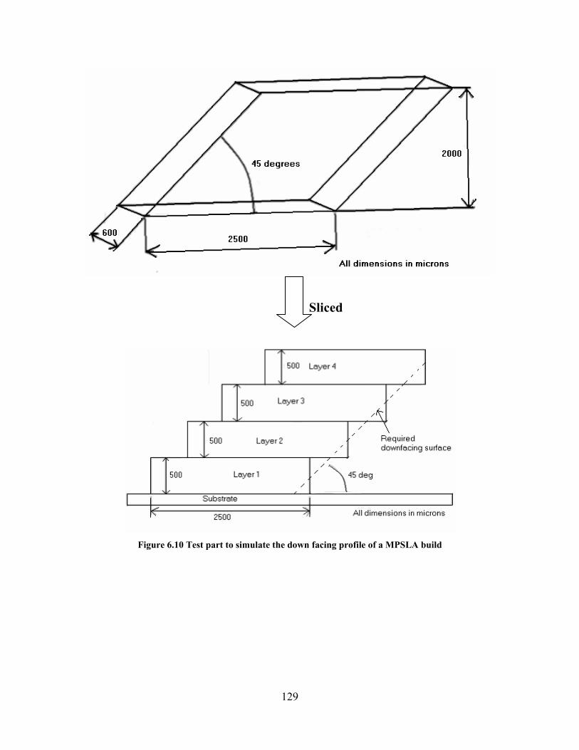
129
Sliced
Figure 6.10 Test part to simulate the down facing profile of a MPSLA build

130
Figure 6.11 (a) Bitmap to be displayed to cure the required layer; (b) Irradiance distribution on resin
surface upon imaging the bitmap
The irradiance (H) at the center of every pixel on the resin surface was obtained
from the irradiance distribution as shown in Figure 6.11. The minimum irradiance across
the irradiance profile is at its left-most edge, equal to 0.47mW/cm2. In order to ensure
that the layer at this location cures down and binds to the layer underneath it, the time of
exposure for the layers is calculated to be 80s, by using equation 6.5. Every layer is alike
and was built by imaging the same bitmap on the resin surface for the same time of
exposure (80s). The layers were built offset by 500µm by translating the platform
laterally under the imaging system. The time allowed for the resin to settle before
exposing any layer was 60s, i.e. tk = 60s. The value of print through at every lateral
location on the built part was computed using equation 6.20 and the down facing surface
was simulated as shown in Figure 6.12. The Matlab code written to generate the
simulated profile is documented in Appendix F.
(a) Bitmap to be imaged (b) Irradiance distribution on resin surface
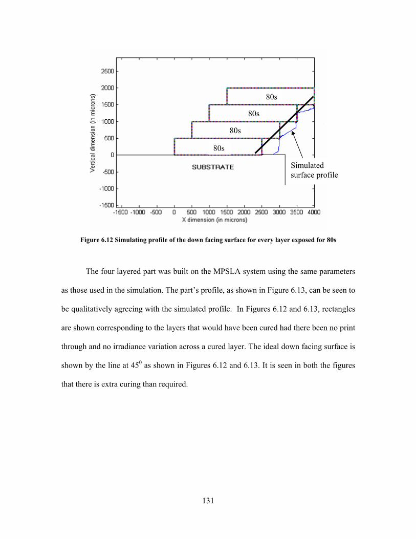
131
Figure 6.12 Simulating profile of the down facing surface for every layer exposed for 80s
The four layered part was built on the MPSLA system using the same parameters
as those used in the simulation. The part’s profile, as shown in Figure 6.13, can be seen to
be qualitatively agreeing with the simulated profile. In Figures 6.12 and 6.13, rectangles
are shown corresponding to the layers that would have been cured had there been no print
through and no irradiance variation across a cured layer. The ideal down facing surface is
shown by the line at 450 as shown in Figures 6.12 and 6.13. It is seen in both the figures
that there is extra curing than required.
80s
80s
80s
80s
Simulated surface profile

132
Figure 6.13 Profile of experimentally cured part with every layer exposed for 80s
Explaining the disparity between experimental and analytical results
It can be seen from Figures 6.12 to 6.13 that the cured surface is smoother than
the simulated surface. The author surmises that it is because of partially cured
photopolymer lodged in between the nooks of the down facing surface. The simulation is
based on the threshold model of resin cure and ignores any partial curing that might
occur. The threshold model makes the assumption that there is a sharp transition between
liquid and solid resin at the threshold exposure of polymerization. In reality, the phase
change occurs over a range of exposure centered about the threshold exposure of
polymerization. As a result, exposures approaching but not yet Ec, result in the formation
of viscous, partially polymerized gels. The author surmises that this gel gets lodged in
between the stair-steps on the down-facing surface, as shown in the simulations and ends
up creating a fillet, thereby smoothing the surface.
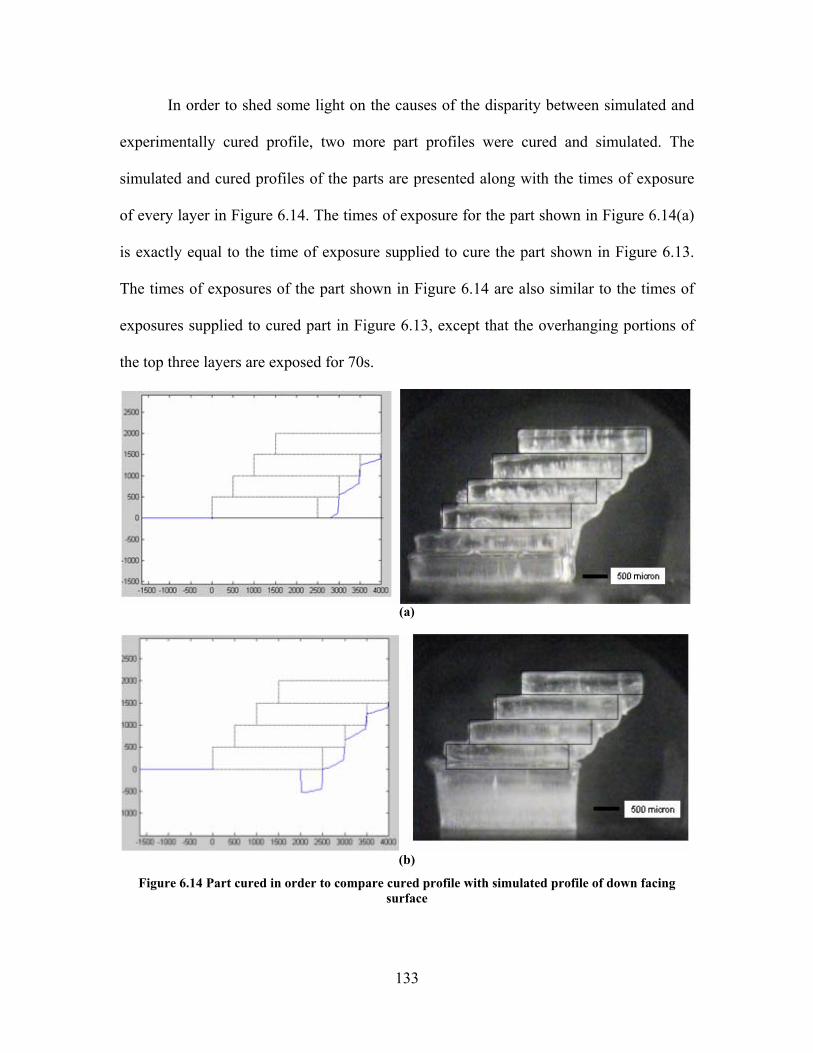
133
In order to shed some light on the causes of the disparity between simulated and
experimentally cured profile, two more part profiles were cured and simulated. The
simulated and cured profiles of the parts are presented along with the times of exposure
of every layer in Figure 6.14. The times of exposure for the part shown in Figure 6.14(a)
is exactly equal to the time of exposure supplied to cure the part shown in Figure 6.13.
The times of exposures of the part shown in Figure 6.14 are also similar to the times of
exposures supplied to cured part in Figure 6.13, except that the overhanging portions of
the top three layers are exposed for 70s.
(a)
(b)
Figure 6.14 Part cured in order to compare cured profile with simulated profile of down facing surface

134
The profiles of the parts cured in Figures 6.13 and 6.14 are superimposed on the
simulated profile for comparison. The superimposed profiles are shown in Figure 6.15.
(a) Profile of part in Figure 6.13
Figure 6.15 Comparison of the profiles of cured and simulated down facing surfaces
(b) Profile of part in Figure 6.14 (a)
Figure 6.15 (continued)
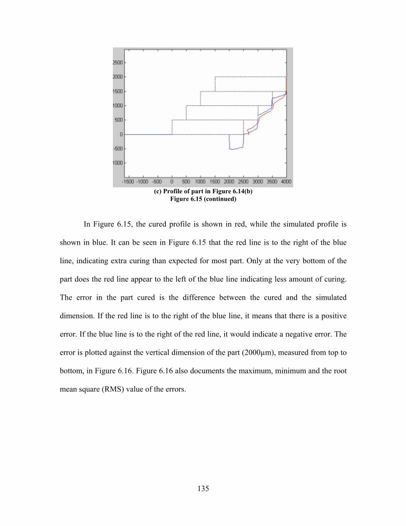
135
(c) Profile of part in Figure 6.14(b)
Figure 6.15 (continued)
In Figure 6.15, the cured profile is shown in red, while the simulated profile is
shown in blue. It can be seen in Figure 6.15 that the red line is to the right of the blue
line, indicating extra curing than expected for most part. Only at the very bottom of the
part does the red line appear to the left of the blue line indicating less amount of curing.
The error in the part cured is the difference between the cured and the simulated
dimension. If the red line is to the right of the blue line, it means that there is a positive
error. If the blue line is to the right of the red line, it would indicate a negative error. The
error is plotted against the vertical dimension of the part (2000µm), measured from top to
bottom, in Figure 6.16. Figure 6.16 also documents the maximum, minimum and the root
mean square (RMS) value of the errors.

136
(a) Error plot for part presented in Figure 6.13
Figure 6.16 Plot of error in lateral direction of cured parts plotted against the vertical dimension of the part
(b) Error plot for part presented in Figure 6.14(a)
Figure 6.16 (continued)
Max error = 220µm Min error = -80µm RMS error =91.7µm
Max error = 350µm Min error = -160µm RMS error =127.5µm
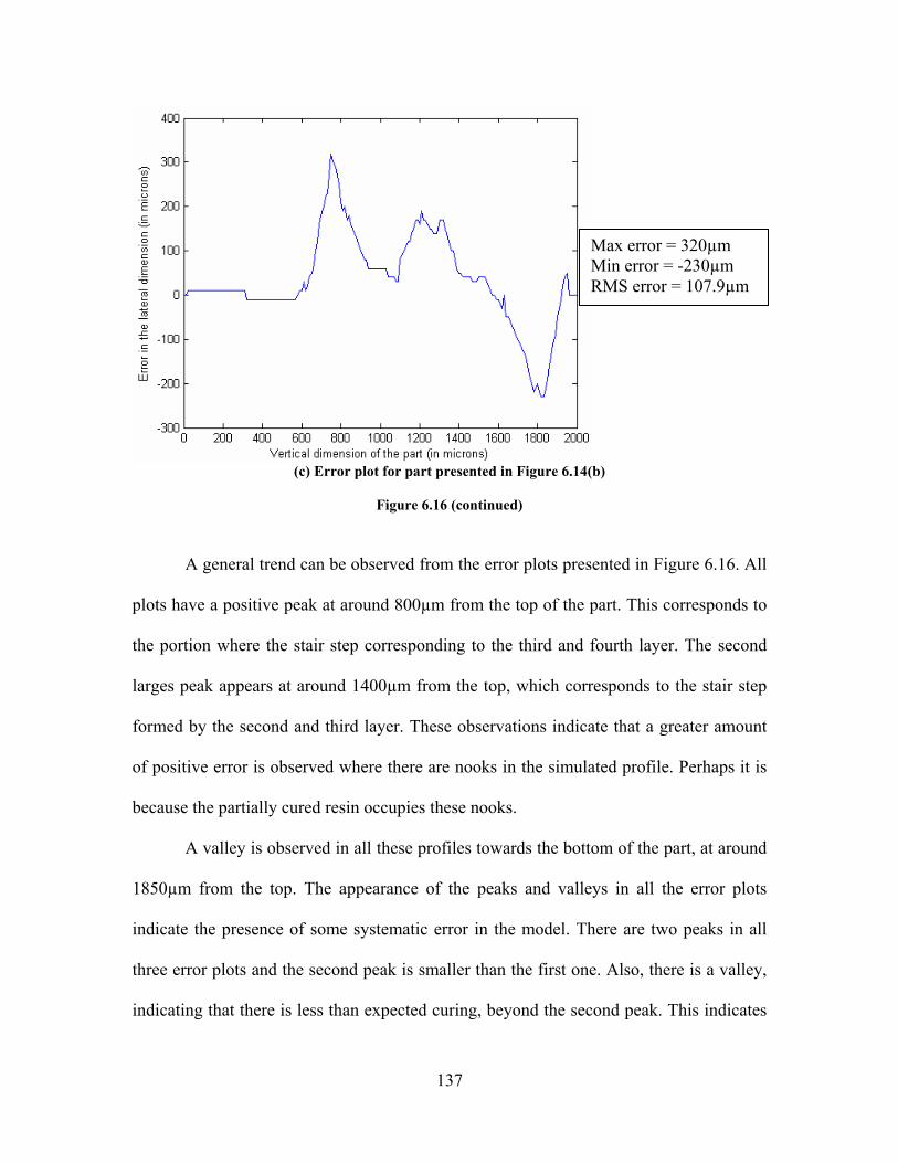
137
(c) Error plot for part presented in Figure 6.14(b)
Figure 6.16 (continued)
A general trend can be observed from the error plots presented in Figure 6.16. All
plots have a positive peak at around 800µm from the top of the part. This corresponds to
the portion where the stair step corresponding to the third and fourth layer. The second
larges peak appears at around 1400µm from the top, which corresponds to the stair step
formed by the second and third layer. These observations indicate that a greater amount
of positive error is observed where there are nooks in the simulated profile. Perhaps it is
because the partially cured resin occupies these nooks.
A valley is observed in all these profiles towards the bottom of the part, at around
1850µm from the top. The appearance of the peaks and valleys in all the error plots
indicate the presence of some systematic error in the model. There are two peaks in all
three error plots and the second peak is smaller than the first one. Also, there is a valley,
indicating that there is less than expected curing, beyond the second peak. This indicates
Max error = 320µm Min error = -230µm RMS error = 107.9µm

138
that the print through model formulated in this research is consistently over-computing
print through as we go towards the bottom of the part. The author speculates that this is
because the rate of radiation attenuation through a cured layer is not exactly zero, as
assumed in the print through model. Some amount of finite loss of energy occurs as the
radiation travels through the cured layers. This error gets compounded towards the
bottom regions of the part which receive radiation penetrating to it through larger cured
depths.
The maximum error along the part profiles can be seen to be varying from 220µm
to 350µm. The minimum error varies from -230µm to -80µm. Thus, the presence of some
random errors can also be seen. From the error plots, the following conclusions can be
drawn:
1. There is some extra curing expected at the location where the simulated profile
predicts a nook.
2. The amount of extra curing is expected to be a couple of hundreds of µm
3. Some negative error is expected towards the bottom of the part. It is expected to
be a couple of hundreds of µm too.
6.5 Compensation zone approach: Inverse print-through model
Now that the simulation of print through and hence the down-facing surface is
validated, it is possible to solve equation (6.22) in order to determine the values of layer
thicknesses and times of exposures to build a dimensionally accurate part. In this section
the compensation zone approach is formulated and demonstrated on a test part.
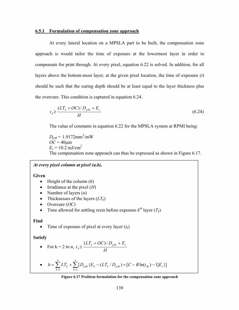
139
6.5.1 Formulation of compensation zone approach
At every lateral location on a MPSLA part to be built, the compensation zone
approach is would tailor the time of exposure at the lowermost layer in order to
compensate for print through. At every pixel, equation 6.22 is solved. In addition, for all
layers above the bottom-most layer, at the given pixel location, the time of exposure (t)
should be such that the curing depth should be at least equal to the layer thickness plus
the overcure. This condition is captured in equation 6.24.
H
EDOCLTt cpMk
k
++≥
/)( (6.24)
The value of constants in equation 6.22 for the MPSLA system at RPMI being:
DpM = 1.9172mm3/mW OC = 40µm Ec = 10.2 mJ/cm2 The compensation zone approach can thus be expressed as shown in Figure 6.17.
Figure 6.17 Problem formulation for the compensation zone approach
At every pixel column at pixel (a,b), Given
• Height of the column (h) • Irradiance at the pixel (H) • Number of layers (n) • Thicknesses of the layers (LTk) • Overcure (OC) • Time allowed for settling resin before exposure kth layer (Tk)
Find
• Time of exposure of pixel at every layer (tk)
Satisfy
• For k = 2 to n, H
EDOCLTt cpMk
k
++≥
/)(
• ]}]1)ln([)/({[11∑∑==
−−+−+=n
kcdkpMkkpM
n
kk EtBCDLTEDLTh

140
6.5.2 Demonstration of compensation zone approach
Suppose we want to compute the exact profile of the part as shown in Figure 6.10.
The down-facing surface is to be linear, as opposed to an approximation to linear surface.
This can be achieved by applying the compensation zone approach at every pixel location
of the part.
The part consists of four rectangular layers of dimensions 2500µmX600µm and
500µm thick. The same bitmap is used to cure every layer. The layers are offset from
each other by 500µm along their lengths by translating the build underneath the imaging
system. The bitmap to be displayed on the DMD is generated by applying the inverse
irradiance model, presented in Section 5.4. The bitmap generated and the irradiance
distribution on the resin surface upon imaging this bitmap onto the resin surface is shown
in Figure 6.11.
Thus, all the inputs to the Compensation zone problem formulation, as presented
in Figure 6.17 are available as follows:
• Height of the pixel column (h): Obtained from the geometry of the part
• Irradiance at every pixel (H) : Generated using the irradiance model
• Number of layers (n) = 4
• Thickness of every layer (LTk) = 500µm
• Overcure (OC) = 40µm
• Settling time before imaging every layer (Tk) = 60s
The unknowns in the problem formulation are the times of imaging of every micro
mirror. For simplification, the time of exposure of the “bodies” of all the layers, as shown

141
in Figure 6.10, i.e. the portion of every layer that binds to the layer underneath it is
assumed to be 80s.
At every pixel location, with the values of tk for all layers but the bottom most
layer computed as 80s, the value of the time of exposure for the micro mirror at the
bottom-most layer (t1) at that pixel location can be determined by solving equation 6.22,
re-written here.
]}]1)ln([)/({[11∑∑==
−−+−+=n
kcdkpMkkpM
n
kk EtBCDLTEDLTh (6.22)
The Matlab code implementing the Compensation zone approach at every micro
mirror location is presented in Appendix G. The time of exposure for every layer is
plotted against the X dimension of that layer as shown in Figure 6.18.
(a) Time of exposure across first layer
Figure 6.18 Times of exposure of the (a) first; (b) second; (c) third; and (d) fourth layer
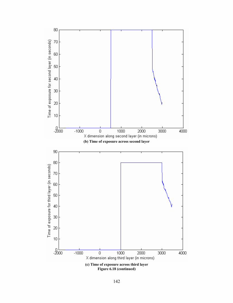
142
(b) Time of exposure across second layer
(c) Time of exposure across third layer
Figure 6.18 (continued)
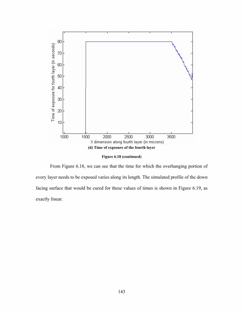
143
(d) Time of exposure of the fourth layer
Figure 6.18 (continued)
From Figure 6.18, we can see that the time for which the overhanging portion of
every layer needs to be exposed varies along its length. The simulated profile of the down
facing surface that would be cured for these values of times is shown in Figure 6.19, as
exactly linear.

144
Figure 6.19 Simulated profile of the down facing surface for the times of exposure as given in Figure
6.18
In order to supply the times of exposure as given in Figure 6.18, it would be
necessary to display and image every micro-mirror on the bitmap irradiating the
overhanging portion of the layer separately for a given duration of time. Since this is not
possible to do manually, the author computed the average time of exposure across the
overhanging portion of the bitmap. This has been illustrated in Figure 6.20.
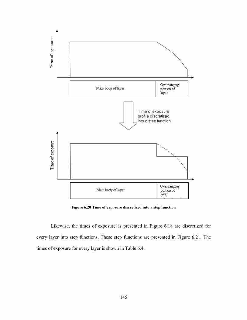
145
Figure 6.20 Time of exposure discretized into a step function
Likewise, the times of exposure as presented in Figure 6.18 are discretized for
every layer into step functions. These step functions are presented in Figure 6.21. The
times of exposure for every layer is shown in Table 6.4.

146
0 1000 2000 3000 4000 5000 60000
10
20
30
40
50
60
70
80
X dimension of the part (in microns)
Tim
e of
exp
osur
e of
Lay
er #
1 (i
n se
cond
s)
(a) Time of exposure for first layer approximated by a step function
Figure 6.21 Times of exposure for the (a) first; (b) second; (c) third; and (d) fourth layer approximated by a step function
0 1000 2000 3000 4000 5000 60000
10
20
30
40
50
60
70
80
X dimension of the part (in microns)
Tim
e of
exp
osur
e of
Lay
er #
2 (i
n se
cond
s)
(b) Time of exposure for second layer approximated by a step function
Figure 6.21 (continued)
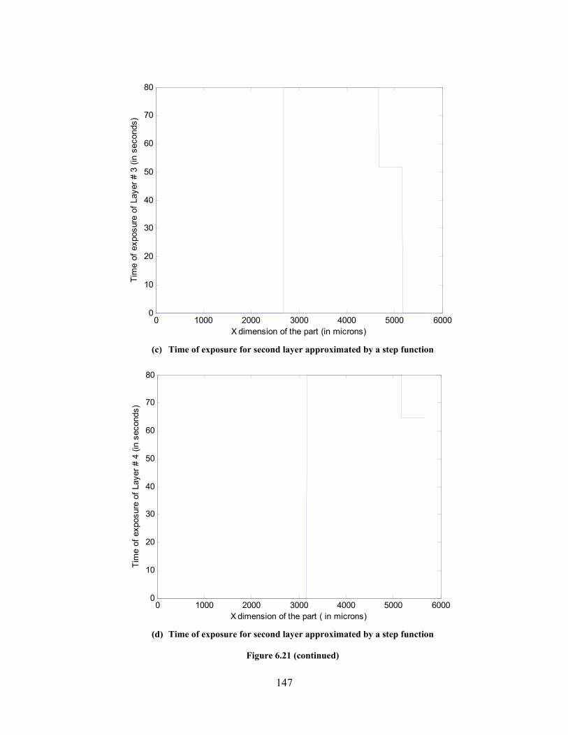
147
0 1000 2000 3000 4000 5000 60000
10
20
30
40
50
60
70
80
X dimension of the part (in microns)
Tim
e of
exp
osur
e of
Lay
er #
3 (i
n se
cond
s)
(c) Time of exposure for second layer approximated by a step function
0 1000 2000 3000 4000 5000 60000
10
20
30
40
50
60
70
80
X dimension of the part ( in microns)
Tim
e of
exp
osur
e of
Lay
er #
4 (i
n se
cond
s)
(d) Time of exposure for second layer approximated by a step function
Figure 6.21 (continued)
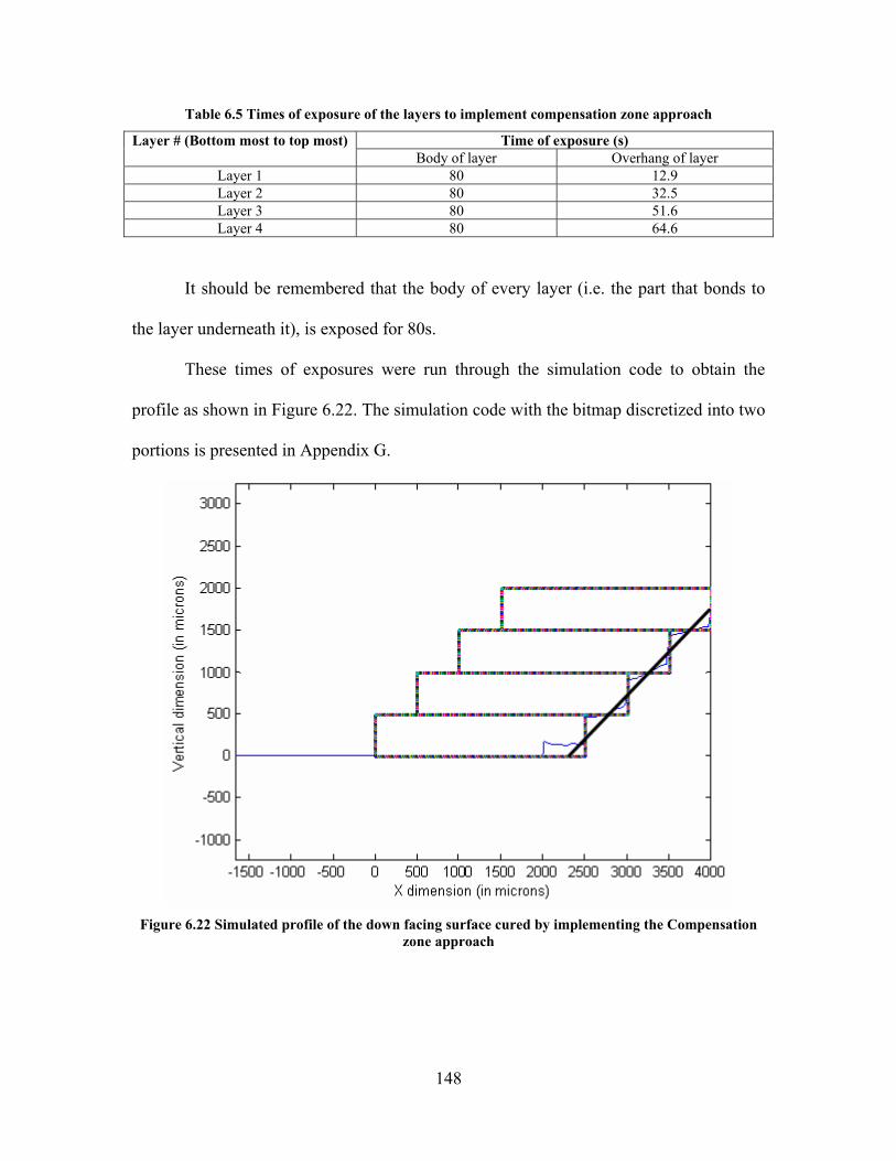
148
Table 6.5 Times of exposure of the layers to implement compensation zone approach
Time of exposure (s) Layer # (Bottom most to top most) Body of layer Overhang of layer
Layer 1 80 12.9 Layer 2 80 32.5 Layer 3 80 51.6 Layer 4 80 64.6
It should be remembered that the body of every layer (i.e. the part that bonds to
the layer underneath it), is exposed for 80s.
These times of exposures were run through the simulation code to obtain the
profile as shown in Figure 6.22. The simulation code with the bitmap discretized into two
portions is presented in Appendix G.
Figure 6.22 Simulated profile of the down facing surface cured by implementing the Compensation
zone approach
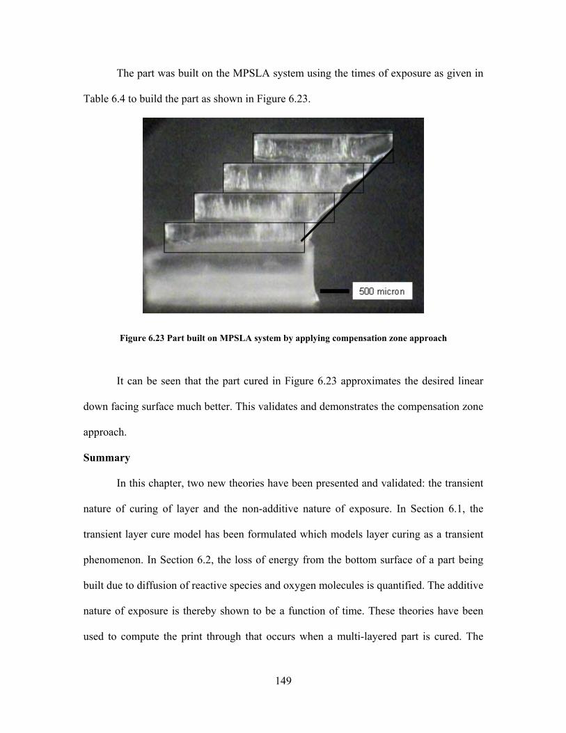
149
The part was built on the MPSLA system using the times of exposure as given in
Table 6.4 to build the part as shown in Figure 6.23.
Figure 6.23 Part built on MPSLA system by applying compensation zone approach
It can be seen that the part cured in Figure 6.23 approximates the desired linear
down facing surface much better. This validates and demonstrates the compensation zone
approach.
Summary
In this chapter, two new theories have been presented and validated: the transient
nature of curing of layer and the non-additive nature of exposure. In Section 6.1, the
transient layer cure model has been formulated which models layer curing as a transient
phenomenon. In Section 6.2, the loss of energy from the bottom surface of a part being
built due to diffusion of reactive species and oxygen molecules is quantified. The additive
nature of exposure is thereby shown to be a function of time. These theories have been
used to compute the print through that occurs when a multi-layered part is cured. The

150
compensation zone approach is presented as a method to avoid the print though errors
and build parts with accurate down-facing surfaces.
Progress made towards answering the research questions
Research question 2(a) dealt with the transient nature of layer curing.
Conventional SLA theory assumes the rate of radiation attenuation with respect to
distance to be constant during exposure. Layer curing is hypothesized in this chapter to
be a transient curing process, in which the rate of attenuation of radiation with respect to
distance, goes on varying during exposure. This hypothesis is tested by modeling the
curing as a transient process, by discretizing the time domain. A differential equation
relating the increment in cure depth with the increment in time is formulated and solved
numerically. The resin constants are determined by curing test layers.
Research question 2(b) was concerning the additive nature of exposure.
Conventional SLA theory assumes that exposure is additive, meaning that the effect of
two discrete exposure doses on cure depth is the same that of a single, combined
exposure dose. The author has hypothesized that the additive nature of exposure is a
strong function of time. It has been shown in this chapter that when the layer remains in
the resin in between the two exposures, there is a significant loss of energy from the
bottom surface of the layer. This loss of energy is shown to vary as the logarithm of the
time for which the layer sits in the resin. Thus, it has been shown that some diffusion
based phenomenon is at work for reducing the energy available at the bottom surface of
the layer. Thus, the additive nature of exposure is shown to be a function of time.
151
CHAPTER 7 SURFACE FINISH OF MASK PROJECTION STEREOLITHOGRAPHY BUILDS
Surface finish is rougher along the z-axis of RP parts than parallel to the xy-plane
because of the “stair stepping” effect (Paul and Voorakarnam, 2001). In this chapter,
methods to improving surface finish and to achieve a trade off between surface finish and
build time of MPSLA builds is presented. The issues of improvement of surface finishes
of up- and down facing surfaces have been handled separately in this chapter.
In case of down facing surfaces, print through results in filleting in the stair steps,
thereby smoothing the down facing surface (Reeves and Cobb, 1999). This has also been
observed by the author in this dissertation (Chapter 6). Research Question 3 was
regarding employing print through smoothing to approximate the vertical profiles of
MPSLA builds beyond the approximation possible by the stair steps created by layers, by
modulating the exposure supplied at the edges of the layers. This method of modulating
the exposure to better approximate down facing surface is referred to, in this dissertation,
as the “adaptive exposure” method. In Section 7.1, and adaptive exposure method to
improve surface finish of a down facing surface is explained in detail and is demonstrated
on a test part.
The surface finish of up-facing surfaces of MPSLA parts is limited by the stair
stepping phenomena. There is no print through to smoothen out the top facing surface.
Meniscus smoothing, in which the resin meniscus lodged between the stair steps is cured,
is proposed as a method to smoothen up facing surfaces (Cobb and Reeves, 1997), but
this method is not repeatable and controllable. Thus, the only method to improve the
surface finish of up facing surfaces is to use thinner layers to build the part. This
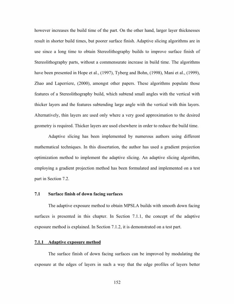
152
however increases the build time of the part. On the other hand, larger layer thicknesses
result in shorter build times, but poorer surface finish. Adaptive slicing algorithms are in
use since a long time to obtain Stereolithography builds to improve surface finish of
Stereolithography parts, without a commensurate increase in build time. The algorithms
have been presented in Hope et al., (1997), Tyberg and Bohn, (1998), Mani et al., (1999),
Zhao and Laperriere, (2000), amongst other papers. These algorithms populate those
features of a Stereolithography build, which subtend small angles with the vertical with
thicker layers and the features subtending large angle with the vertical with thin layers.
Alternatively, thin layers are used only where a very good approximation to the desired
geometry is required. Thicker layers are used elsewhere in order to reduce the build time.
Adaptive slicing has been implemented by numerous authors using different
mathematical techniques. In this dissertation, the author has used a gradient projection
optimization method to implement the adaptive slicing. An adaptive slicing algorithm,
employing a gradient projection method has been formulated and implemented on a test
part in Section 7.2.
7.1 Surface finish of down facing surfaces
The adaptive exposure method to obtain MPSLA builds with smooth down facing
surfaces is presented in this chapter. In Section 7.1.1, the concept of the adaptive
exposure method is explained. In Section 7.1.2, it is demonstrated on a test part.
7.1.1 Adaptive exposure method
The surface finish of down facing surfaces can be improved by modulating the
exposure at the edges of layers in such a way that the edge profiles of layers better

153
approximate the down facing profile of the part. To demonstrate the adaptive exposure
method, we consider the same test part as used to demonstrate the compensation zone
approach in Chapter 6. The reader can refer to the four layered part, with up-and down
facing surfaces at 450 to the horizontal is shown in Figure 6.10. This part was sliced into
layers 500µm thick. The time of exposure of these layers was computed using the
compensation zone approach in Section 6.5.2. The times of exposure for every layer have
been plotted against their X dimensions in Figure 6.18. In implementing the
compensation zone approach, the author averaged the time of exposure along the
overhanging portion of every layer. Thus, every layer was cured by exposing it in two
steps. In the first step, the body of the layer (the part which binds to the layer underneath
it) was exposed for certain duration of time so that the layers bind to each other. In the
second step, the overhanging portion of the layer was exposed for a duration equal to that
obtained by averaging out the time of exposure across it, presented in Figure 6.21. This
method has been pictorially explained in Chapter 6, in Figure 6.20. The simulated profile
of the part that will be cured by implementing the compensation zone has been presented
in Figure 6.22 and the actually cured part has been presented in Figure 6.23. From both
these figures, we can see than the approximation to the down facing profile is not exact.
Also, the effect of stair steps is visible.
A better approximation can be obtained by modulating the exposure at the
overhanging portion of every layer. This can be achieved by discretizing the overhanging
portion of every layer into two regions. The time of exposure can be averaged out along
these two regions separately. This is illustrated in Figure 7.1. Thus, every layer will be
cured in three steps. In the first step, the body of the layer will be cured for a time
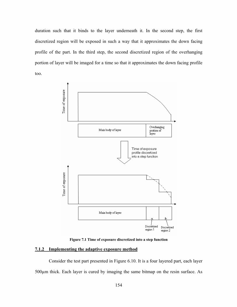
154
duration such that it binds to the layer underneath it. In the second step, the first
discretized region will be exposed in such a way that it approximates the down facing
profile of the part. In the third step, the second discretized region of the overhanging
portion of layer will be imaged for a time so that it approximates the down facing profile
too.
Figure 7.1 Time of exposure discretized into a step function
7.1.2 Implementing the adaptive exposure method
Consider the test part presented in Figure 6.10. It is a four layered part, each layer
500µm thick. Each layer is cured by imaging the same bitmap on the resin surface. As
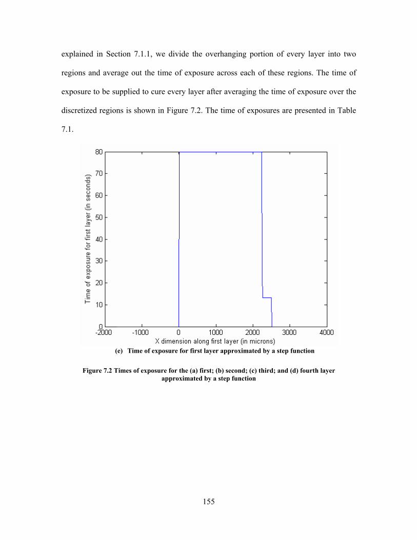
155
explained in Section 7.1.1, we divide the overhanging portion of every layer into two
regions and average out the time of exposure across each of these regions. The time of
exposure to be supplied to cure every layer after averaging the time of exposure over the
discretized regions is shown in Figure 7.2. The time of exposures are presented in Table
7.1.
(e) Time of exposure for first layer approximated by a step function
Figure 7.2 Times of exposure for the (a) first; (b) second; (c) third; and (d) fourth layer approximated by a step function

156
(f) Time of exposure for second layer approximated by a step function
(g) Time of exposure for second layer approximated by a step function
Figure 7.2 (continued)

157
(h) Time of exposure for second layer approximated by a step function
Figure 7.2 (continued)
Table 7. 1 Times of exposure of the layers to implement the adaptive exposure method
Time of exposure (s) Layer # (bottom most to top most) Body of layer Overhang (Discretized region 1) Overhang (Discretized region 2)
Layer 1 80 12.9 -- Layer 2 80 40.1 26.3 Layer 3 80 56.4 46.8 Layer 4 80 71.8 57.4
Note that due to the nature of slicing, there is only one discretized region for the
bottom most layer.
The down facing profile of the part that would be built with these times of
exposure was simulated by implementing the print through model. The simulated profile
is presented in Figure 7.3. The Matlab code for this simulation is documented in
Appendix H.

158
Figure 7.3 Simulated profile of the down facing surface after discretizing the overhanging portion of
every layer into two parts and applying compensation zone approach at every part
The part was built on the MPSLA system using the said times of exposures to obtain the
part as shown in Figure 7.4.
Figure 7.4 Part built on MPSLA system by applying compensation zone approach by discretizing the
bitmap into three regions
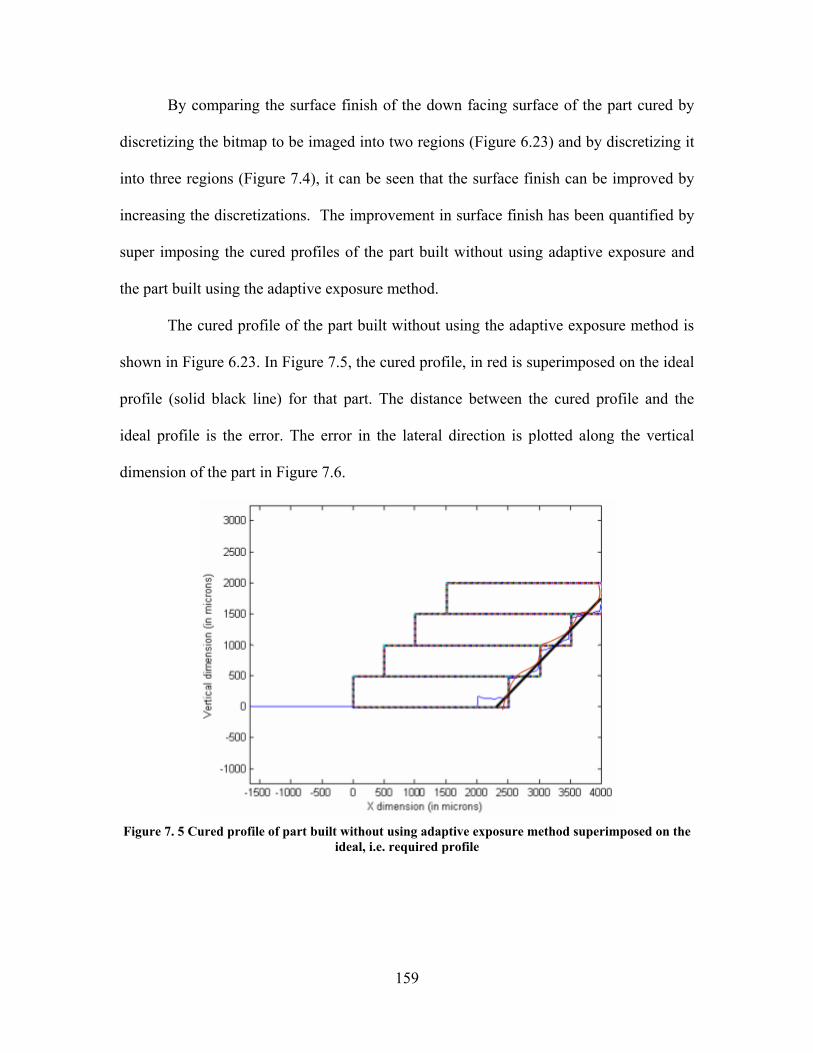
159
By comparing the surface finish of the down facing surface of the part cured by
discretizing the bitmap to be imaged into two regions (Figure 6.23) and by discretizing it
into three regions (Figure 7.4), it can be seen that the surface finish can be improved by
increasing the discretizations. The improvement in surface finish has been quantified by
super imposing the cured profiles of the part built without using adaptive exposure and
the part built using the adaptive exposure method.
The cured profile of the part built without using the adaptive exposure method is
shown in Figure 6.23. In Figure 7.5, the cured profile, in red is superimposed on the ideal
profile (solid black line) for that part. The distance between the cured profile and the
ideal profile is the error. The error in the lateral direction is plotted along the vertical
dimension of the part in Figure 7.6.
Figure 7. 5 Cured profile of part built without using adaptive exposure method superimposed on the
ideal, i.e. required profile

160
Figure 7. 6 Error in the lateral direction of the part built without using adaptive exposure
The cured profile of the part built using the adaptive exposure method is shown in
Figure 7.4. In Figure 7.7, the cured profile, in red is superimposed on the ideal profile
(solid black line) for that part. The distance between the cured profile and the ideal
profile is the error. The error in the lateral direction is plotted along the vertical
dimension of the part in Figure 7.8.
Max error = 110µm Min error = -250µm RMS error = 104.2µm

161
Figure 7. 7 Cured profile of part built using adaptive exposure method superimposed on the ideal, i.e.
required profile
Figure 7. 8 Error in the lateral direction of the part built using adaptive exposure
From Figures 7.6 and 7.8, it can be seen that there are more fluctuations in the
error profile in case of the part built without using adaptive exposure method. In case of
the part built using the adaptive exposure method, the fluctuations can be seen to be less.
However, a systematic error can be observed in the part built using the adaptive exposure
Max error = 220µm Min error = -70µm RMS error = 89.3µm

162
method. The positive error in the lateral direction can be seen to be increasing from top of
the part to the bottom of the part.
Thus the adaptive exposure method has been shown to improve the surface finish
of the test part. However, a systematic error in observed in the part built with adaptive
exposure, in which the amount of positive deviation from the ideal profile goes on
increasing from the top to bottom.
7.2 Surface finish of up facing surfaces
Surface finish of an up-facing surface and the build time of a MPSLA part are
directly affected by the layer thicknesses. In choosing a slicing scheme, a process planner
needs to achieve a trade-off between surface finish and build time. In this section, an
adaptive slicing algorithm employing a gradient projection optimization method is
formulated and implemented on a test part. In Section 7.2.1, the tradeoff between the two
objectives of build time and surface finish is modeled as a compromise Decision Support
Problem (cDSP), which is a multi-objective optimization problem. In Section 7.2.2,
Rosen’s gradient projection method (Belegundu and Chandrupatla, 1999) is explained as
a method to solve the multi-objective optimization problem. In Section 7.2.3, the adaptive
slicing algorithm employing the gradient projection method is presented. The slicing
algorithm is implemented on a test part in Section 7.2.4.
7.2.1 Formulating a multi-objective optimization
Consider a general MPSLA system that can lay down layers as thin as LTmin and
as thick as LTmax. Let the height of a MPSLA part to be built be h units. The variables for
this problem are the thickness of every layer, with the bounds on the layers being LTmin
163
and LTmax. Another related variable is the number of layers n. The constraint on the part is
an equality constraint, which states that the summation of all the layers is equal to the
height of the part h. The variables and constraints are summarized as:
Variables:
],[
],[
minmax
maxmin
LTh
LThn
LTLTLT
∈
∈ (7.1)
Constraints:
hLTn
kk =∑
=1 (7.2)
We now derive the objective functions of surface finish and build time.
7.2.1.1 Derivation of objective function for surface finish Consider a MPSLA part sliced as shown in Figure 7.9. The thickness of every
layer that this part is sliced into is given as LT1, LT2 … LTn. The lateral axis is denoted as
“R” and the vertical axis is denoted as “Z”. The vertical profile of the part is given by
)(rfz = (7.3)
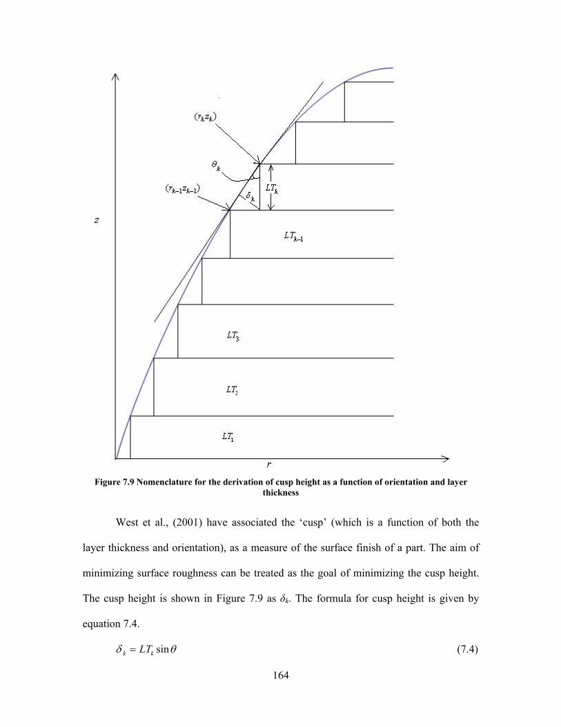
164
Figure 7.9 Nomenclature for the derivation of cusp height as a function of orientation and layer
thickness
West et al., (2001) have associated the ‘cusp’ (which is a function of both the
layer thickness and orientation), as a measure of the surface finish of a part. The aim of
minimizing surface roughness can be treated as the goal of minimizing the cusp height.
The cusp height is shown in Figure 7.9 as δk. The formula for cusp height is given by
equation 7.4.
δ θk kLT= sin (7.4)
165
In general, if the vertical profile of a part is given by the function z = f(r), the Z-
coordinate of the (k-1)th layer will be zk-1 given by equation
z LTk ii
k
−=
−
= ∑11
1
(7.5)
and that of the kth layer will be zk given by equation
z LTk ii
k
==∑
1
(7.6)
The r-coordinates of the points on the intersection of the k-1th and kth layer would be
given by equations
r f zk k−−
−=11
1( )
r f zk k= −1( ) (7.7)
The angle θ as shown in Figure 7.9 would thus be given by equation
θ kk k
k k
r rz z
=−−
− −
−
tan ( )1 1
1
θ kk k
k
r rLT
=−− −tan ( )1 1 (7.8)
The cusp height at the kth layer would be given by equation
δ θk k kLT= sin( ) (7.9)
The maximum cusp height will be given by
]max[max kδδ = , k 1 to n (7.10)
Thus, the first objective: “to minimize the surface finish”, is given in terms of the
variables LTk and n by making substitutions from equation 7.5 to 7.10 as:
166
Objective 1:
Minimize
)}])()(
(sin{tanmax[ 1
1
1
11
1max
k
k
i
k
iii
k LT
LTfLTfLT
∑ ∑=
−
=
−−
−
−=δ (7.11)
7.2.1.2 Derivation of objective function for build time Chen and Sullivan, (1996) formulated an algorithm to predict build time of
Stereolithography parts by using detailed scan and recoat information from the build
files. Other researchers have also quantified build time. All of them have broken down
the part building process into its constituent steps and modeled the time required to
complete each of these steps.
The build time of an MPSLA build can be calculated by breaking down the
process of building a part into its constituent steps. A MPSLA part is built by performing
the following steps for every layer cured:
1. Lower platform into resin (Deep dip). Translate the platform underneath the
recoater blade, raise it to the required level and bring it back to the required
position.
2. Wait for the resin film to settle to its final thickness. This is a function of the layer
thickness.
3. Expose the layer for the required time. This time is a function of the layer
thickness.
The first step involves the translation of the platform and will take approximately
the same time, regardless of the layer thickness. Let us denote this time as Ttrans. After the
second step, there is a slight bulge on top of the part being cured (Jacobs, 1992). The
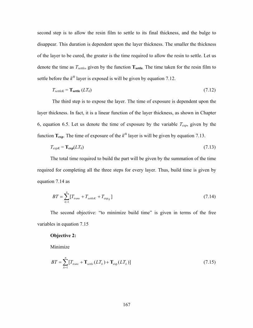
167
second step is to allow the resin film to settle to its final thickness, and the bulge to
disappear. This duration is dependent upon the layer thickness. The smaller the thickness
of the layer to be cured, the greater is the time required to allow the resin to settle. Let us
denote the time as Tsettle, given by the function Tsettle. The time taken for the resin film to
settle before the kth layer is exposed is will be given by equation 7.12.
TsettleK = Tsettle (LTk) (7.12)
The third step is to expose the layer. The time of exposure is dependent upon the
layer thickness. In fact, it is a linear function of the layer thickness, as shown in Chapter
6, equation 6.5. Let us denote the time of exposure by the variable Texp, given by the
function Texp. The time of exposure of the kth layer is will be given by equation 7.13.
TexpK = Texp(LTk) (7.13)
The total time required to build the part will be given by the summation of the time
required for completing all the three steps for every layer. Thus, build time is given by
equation 7.14 as
∑=
++=n
kksettleKtrans TTTBT
1exp ][ (7.14)
The second objective: “to minimize build time” is given in terms of the free
variables in equation 7.15
Objective 2:
Minimize
)]()([ exp1
kk
n
ksettletrans LTLTTBT TT ++= ∑
=
(7.15)
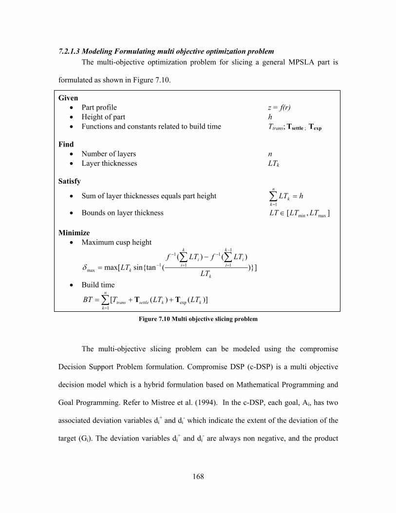
168
7.2.1.3 Modeling Formulating multi objective optimization problem The multi-objective optimization problem for slicing a general MPSLA part is
formulated as shown in Figure 7.10.
Given • Part profile z = f(r) • Height of part h • Functions and constants related to build time Ttrans; Tsettle ; Texp
Find
• Number of layers n • Layer thicknesses LTk
Satisfy
• Sum of layer thicknesses equals part height hLTn
kk =∑
=1
• Bounds on layer thickness ],[ maxmin LTLTLT ∈ Minimize
• Maximum cusp height
)}])()(
(sin{tanmax[ 1
1
1
11
1max
k
k
i
k
iii
k LT
LTfLTfLT
∑ ∑=
−
=
−−
−
−=δ
• Build time
)]()([ exp1
kk
n
ksettletrans LTLTTBT TT ++= ∑
=
Figure 7.10 Multi objective slicing problem
The multi-objective slicing problem can be modeled using the compromise
Decision Support Problem formulation. Compromise DSP (c-DSP) is a multi objective
decision model which is a hybrid formulation based on Mathematical Programming and
Goal Programming. Refer to Mistree et al. (1994). In the c-DSP, each goal, Ai, has two
associated deviation variables di+ and di
- which indicate the extent of the deviation of the
target (Gi). The deviation variables di+ and di
- are always non negative, and the product
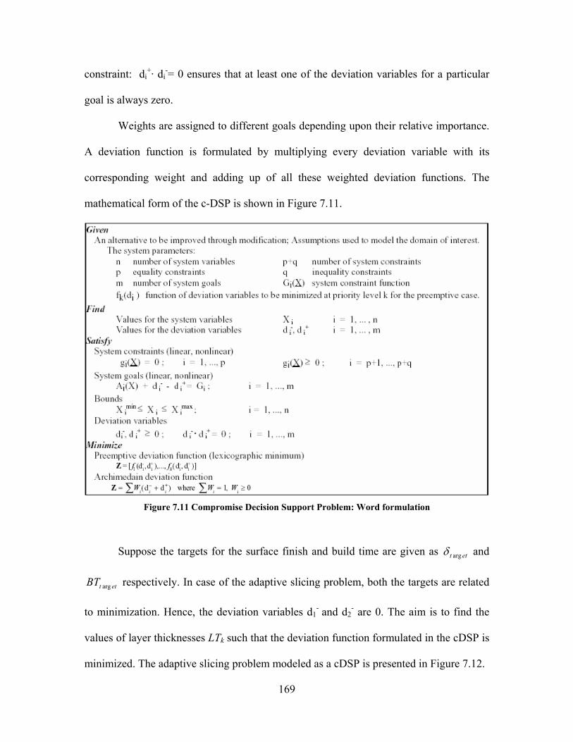
169
constraint: di+· di
-= 0 ensures that at least one of the deviation variables for a particular
goal is always zero.
Weights are assigned to different goals depending upon their relative importance.
A deviation function is formulated by multiplying every deviation variable with its
corresponding weight and adding up of all these weighted deviation functions. The
mathematical form of the c-DSP is shown in Figure 7.11.
Figure 7.11 Compromise Decision Support Problem: Word formulation
Suppose the targets for the surface finish and build time are given as ett argδ and
ettBT arg respectively. In case of the adaptive slicing problem, both the targets are related
to minimization. Hence, the deviation variables d1- and d2
- are 0. The aim is to find the
values of layer thicknesses LTk such that the deviation function formulated in the cDSP is
minimized. The adaptive slicing problem modeled as a cDSP is presented in Figure 7.12.

170
Given • Part profile z = f(r) • Height of part h • Functions and constants related to build time Ttrans; Tsettle ; Texp • Deviation variables 0;0 21 == −− dd
Find • Number of layers n • Layer thicknesses LTk • Deviation variables d1
+, d2+
Satisfy
• Sum of layer thicknesses equals part height hLTn
kk =∑
=1
• Bounds on layer thickness ],[ maxmin LTLTLT ∈
Goals • Meet low target of surface finish
ettk
k
i
k
iii
k ddLT
LTfLTfLT arg11
1
1
1
11
1 )}])()(
(sin{tanmax[ δ=−+−
+−=
−
=
−−
−∑ ∑
• Meet low target for build time
ettkk
n
ksettletrans BTddLTLTT arg22exp
1)]()([ =−+++ +−
=∑ TT
Minimize Deviation function Example scenarios:
• Both goals rated equally: Z d d d d= + + +− + − +12
121 1 2 2( ) ( )
• Surface finish rated more than Build time: Z d d d d= + + +− + − +34
141 1 2 2( ) ( )
• Build time rated more than Surface finish: Z d d d d= + + +− + − +14
341 1 2 2( ) ( )
• Surface finish not important: Z d d d d= ⋅ + + ⋅ +− + − +0 11 1 2 2( ) ( ) • Build time not important: Z d d d d= ⋅ + + ⋅ +− + − +1 01 1 2 2( ) ( )
Figure 7.12 Adaptive slicing problem modeled as a compromise DSP

171
7.2.2 Solution to the cDSP (Rosen’s gradient projection method)
In this chapter, an optimization method to minimize the deviation function of the
cDSP presented in Figure 7.12 is presented. Rosen’s gradient projection Method
(Belegundu and Chandrupatla, 1999) works the best when there is a linear equality
constraint and is hence chosen as the optimization method to solve the cDSP. In Section
7.2.2.1, the theory behind Rosen’s gradient projection method is explained. In Section
7.2.2.2, the method is applied to the adaptive slicing problem at hand.
7.2.2.1 Theory of Rosen’s gradient projection method Consider problems that can be expressed in the form
Minimize f(x)
Subject to aix – bi <=0 i = 1,…., m (7.16)
aix -bi =0 i = m+1, ....., m+l
Let t = number of active constraints, consisting of all the equalities and active
inequalities.
Assume that xk is the current feasible start point, as shown in Figure 7.13. xk lies
on the linear constraint in equation 7.16. The task in any optimization algorithm is to
determine a direction vector d followed by a step length along this direction that would
give us a new and better feasible point. We repeat this iterative process until we arrive at
the optimum. If we are at an interior point then the steepest descent direction is the
obvious choice:−∇f xk( ). After moving along the direction of steepest descent by some
step size, a projection is obtained on the multi- dimensional plane corresponding to the
equality constraint.
172
Figure 7.13 Rosen's gradient projection method
In other words, the direction d is found by projecting the step taken along
−∇f xk( ) in such a way that d−∇− )(xf is the minimum possible. Suppose we define a
matrix B as consisting of rows of the gradient vectors of the active constraint, then we
can get the relation
Bd = 0 (7.17)
Thus, we need the direction d such that which shall be the solution of:
Minimize ))(())(( dd −−∇−−∇ xfxf T (7.18)
Subject to Bd = 0
Defining the Lagrangian Bddd TT ffL β++∇+∇= )()( , we have the optimality
conditions:

173
0)( =++∇=∂∂ βT
T
fL Bdd
(7.19)
Pre-multiplying by B and substituting equation 7.17, we get
fT ∇−= BBB β][ (7.20)
For a detailed explanation of Lagrangian formulations to find exact minimum, please
refer to Belegundu and Chandrupatla, (1999).
From equation 7.19, we can get a relation for the direction d as
βTf Bd −−∇= (7.21)
Substituting the value of β from equation 7.20 into equation 7.21, we get
ff TT ∇+−∇= − BBBBd 1][ (7.22)
Combining the matrices multiplying ( f∇− ), we can write
)( f−∇−= Pd (7.23)
where P is the “projection matrix”, which is given by
]][[ 1BBBBIP −−= TT (7.24)
The vector d obtained by solving equation 7.23 can be shown to be the descent
direction. When the optimum (minimum) point is reached, d becomes equal to 0.
7.2.2.2 Applying Rosen’s gradient projection method for adaptive slicing In case of the problem at hand, the solution is supposed to lie on the equality
(active) constraint LT hkk
n
=∑ =
1
. The starting point is chosen to be any point that satisfied
this constraint. For a given value of number of layers n, we can choose the starting
feasible solution that all the layers are of the same thickness. Thus, the starting solution is
given by equation 7.25.

174
nhLTk = (7.25)
There are bounds on the layer thickness. These bounds are captured in the objective
function by modifying the deviation function by adding penalty functions, as presented in
equation (7.26).
Minimize
Z d d d d Penalty= + + + +− + − +12
121 1 2 2( ) ( )
where Penalty = 109(Penalty1 + Penalty2) (7.26)
where Penalty1 = (LTmin -LTk), if LTk < 50 = 0, otherwise. and Penalty1 = (LTk – LTmax) , if LTk > 1000 = 0, otherwise. where k 1 to n
For a given number of layers (n), the matrix B is a column matrix with n elements, since
there is only one active constraint to consider.
B = [1,1,1,....n times]T (7.27)
The projection matrix P can be obtained from equation (7.24). The gradient of the
objective function at the starting point xk can be obtained numerically. The direction d is
obtained from equation (7.23). The step size is obtained by using a “pattern search”
algorithm (Belegundu and Chandrupatla, 1999). The Matlab code to implement the
gradient projection algorithm has been presented in Appendix I.
The gradient projection method can thus be represented as a black box, with
inputs and outputs as shown in Figure 7.14. Inside the black box, the optimization
process as explained above occurs.

175
Figure 7.14 Rosen's gradient projection method as a black box
7.2.3 Adaptive slicing algorithm
In this section, we present the algorithm used to solve the cDSP presented in
Figure 7.12. Using Rosen’s gradient projection method as a black box, we can optimize
the layer thicknesses, provided we supply to it the number of layers. Thus, the algorithm
is formulated in which we conduct an exhaustive search across the number of layers that
the part can be populated by (n), and find the optimum slicing scheme for every value of
n. The generated optimum slicing schemes can be compared to see which scheme gives
the least value of the deviation function Z in the compromise DSP.
The adaptive slicing algorithm is presented in Figure 7.15.
ROSEN’S GRADIENT
PROJECTION METHOD
Number of layers (n)
Height of part (h)
Vertical profile of part z = f(r)
Starting feasible solution nhLTk /=
Relative priorities given to objectives
Optimum slicing scheme

176
GIVEN: Height of part (h), Vertical profile (f), bounds on layer thickness
[LTmin, LTmax], priorities given to objectives,
Minimum number of layers nmin = h/LTmax
Maximum number of layers nmax = h/LTmin
(where nmin and nmax are closest feasible integers)
FOR Number of layer n = nmin:1:nmax
Starting feasible solution: nhLTk /=
Apply Rosen’s gradient projection method
Generate optimum slicing scheme for number of layers = n
Compute deviation function of the slicing scheme
END
FOR i = nmin:1:nmax
Compare optimum values of dev. functions obtained for all values of n
END
Figure 7.15 Adaptive slicing algorithm
7.2.4 Applying adaptive slicing algorithm to a test problem
Suppose that the bell shaped part as shown in Figure 7.16 needs to be sliced. The
up facing surface of the part can be seen to be composed of two quadratic curves. The
part needs to be built on the MPSLA system realized at RPMI, in such a way that the
build time is less than or equal to 80 minutes and the maximum cusp height is not more
than 40µm. The bounds on the layer thicknesses are assumed to be [60µm, 600µm].
The compromise DSP formulated in Figure 7.8 can be particularized to the
MPSLA build at hand.

177
Figure 7.16 Part to be adaptively sliced
The slicing is effected by executing the algorithm presented in Figure 7.15. We
first determine the values of the constants and functions related to the build time: Ttrans;
Tsettle ; Texp. Ttrans is the time taken by the platform to translate underneath the recoater
and to bring it back to the required position. This translation time has been measured to
be 10s. This time is almost constant regardless of the layer thickness. The function
Tsettle(LTk) returns the time required to settle the free surface of resin, before supplying an
exposure dose to cure it. The time required to settle the resin if the thickness of a layer is
500µm has been timed by the author to be 60s. The time required to settle the resin for
lower layer thicknesses has not been measured and so, we do not have the function Tsettle.
So, we simply assume the function to be inversely proportional to the layer thickness. We
assume the function Tsettle in equation (7.28) for our system to be to be
TsettleK = 30000/LTk (7.28)

178
where
TsettleK is in seconds; and
LTk is in µm
Texp is the function which acts on the layer thickness and return the time of
exposure. This function can be formulated by using the relationship between the cure
depth and exposure, presented in Chapter 6, in equation 6.5.
)( cpM EEDz −⋅= (6.5)
where
where DpM is the slope of the working curve, which is the rate at which the cure- front
propagates into the resin depth, and
Ec is the threshold exposure of polymerization.
For our system,
DpM = 19.172 µm/(mW/cm2), or 1.9172mm3/mW and
Ec = 10.2 mW/cm2
For our system, we have determined that an overcure of 40µm is necessary for the layer
to bind to each other. Thus, the depth of cure is LTk+OC
Rearranging equation 6.5,
cPM EDzE += / (7.29)
Assuming the average irradiance (H) to be 0.7mW/cm2, the function Texp can be
particularized as given in equation 7.30.
7.0/]5.10172.19
40[exp +
+= k
KLT
t (7.30)
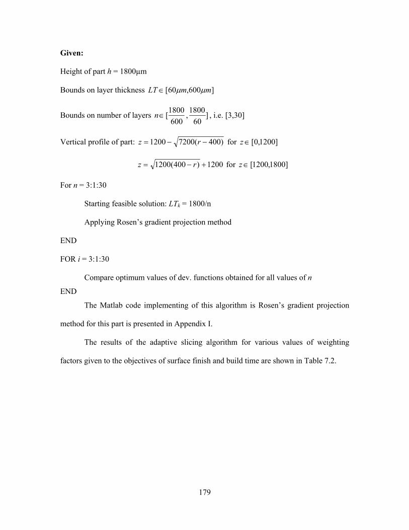
179
Given:
Height of part h = 1800µm
Bounds on layer thickness ]600,60[ mmLT µµ∈
Bounds on number of layers ]60
1800,600
1800[∈n , i.e. [3,30]
Vertical profile of part: )400(72001200 −−= rz for ]1200,0[∈z
1200)400(1200 +−= rz for ]1800,1200[∈z
For n = 3:1:30
Starting feasible solution: LTk = 1800/n
Applying Rosen’s gradient projection method
END
FOR i = 3:1:30
Compare optimum values of dev. functions obtained for all values of n
END
The Matlab code implementing of this algorithm is Rosen’s gradient projection
method for this part is presented in Appendix I.
The results of the adaptive slicing algorithm for various values of weighting
factors given to the objectives of surface finish and build time are shown in Table 7.2.

180
Table 7. 2 Optimum slicing schemes for various priority schemes
Validating the adaptive slicing algorithm
The following observations can be made from the optimum slicing schemes
presented in Table 7.2.
• When weight given to build time is increased and that given to surface finish is
decreased, the optimum number of layers decreases and the layer thicknesses
increase. Conversely, when the weight given to surface finish is increased and that
given to build time is decreased, the optimum number of layers increases and the
layer thicknesses decrease.
• When weight given to the objective of build time is made 1 and that given to the
objective of surface finish is made 0, the optimum slicing scheme comprises of
the thickest possible layers (600µm)
• When weight given to the objective of surface finish is made 1 and that given to
the objective of build time is made 0, the optimum slicing scheme comprises of
the thinnest possible layers (60µm).
• For any scenario, the optimum slicing scheme consists of thicker layers at the
lower portion of the part and thinner layers are the upper top portion. This is
Weights given to Surf. finish
Build time
Optimum no. of layers (n)
Layer thicknesses (µm) Objective function
(Z)
0.5 0.5 14 149.4;149.4;149.4;149.4;149.4;149.4; 149.4;149.4;149.4;148.4;89.2; 66.8;75.6;75.1
0.1419
0.25 0.75 14 149.4;149.4;149.4;149.4;149.4;149.4; 149.4;149.4;149.4;148.4;89.2; 66.8;75.6;75.1
0.0709
0.75 0.25 18 108;108;108;108;108;108;108;108;108;108;108;108;108;108;84.6;74.1; 65.9;62.9
0.1845
1 0 30 60;60;60;60;60;60;60;60;60;60;60;60;60;60;60;60;60;60;60;60;60;60; 60; 60;60;60;60;60;60;60;
0.0331
0 1 3 600;600;600 0
181
because the bottom portion of the vertical profile subtends lesser angle with the
vertical, while the upper portion of the vertical profile subtends a larger angle
with the vertical. Thus, adaptive slicing has been implemented.
All the above observations make intuitive sense and hence, validate the adaptive
slicing algorithm.
Summary
In this chapter, work has been presented on surface finish of MPSLA parts.
Adaptive exposure method is presented as a method to improve the down facing surfaces
of MPSLA builds. This method is an implementation of the Compensation zone
approach, to modulate the exposure supplied to the edge of every layer so that the edge
profile of the layer approximates the MPSLA part’s down facing surface better. The
adaptive exposure method is presented in a test part.
An adaptive slicing algorithm is formulated that slices a CAD model so as to
obtain the required tradeoff between build time and surface finish of up facing surfaces of
the part. This slicing algorithm models the trade off as a compromise Decision Support
Problem (cDSP) and then solves the cDSP by using a gradient projection algorithm. The
slicing algorithm is demonstrated in a test part.
Progress made towards validating research questions
Research question 3 was concerning implementing print through smoothing to
obtain a better approximation to the down facing surface. The adaptive exposure method
is formulated in this chapter to implement print through smoothing on MPSLA parts. The
overhanging portion of every layer of a test part is cured by supplying two separate
exposure doses. The exposure doses are carefully controlled to ensure that the cure

182
profile of the overhanging region of every layer approximates the part’s down facing
surface profile. A part with a better surface finish of the down facing surface is built by
implementing the adaptive slicing algorithm. The RMS deviation from the ideal, or
required surface was improved from 104.2µm to 89.3µm. The fluctuations from the ideal
surface were also significantly reduced, as shown in the error profiles in Figures 7.6 and
7.8. However, a systematic error seems to have been introduced by implementing the
adaptive exposure method, in that the positive error goes on increasing from the top to the
bottom of the part. Thus, the demonstration of adaptive exposure lends support to the
hypothesis that adaptive exposure can be used to effect print through smoothing in
MPSLA builds.

183
CHAPTER 8 CASE STUDY: BUILDING A PART WITH A QUADRATIC VERTICAL PROFILE
Research Question 4 was regarding formulating a process planning method in
order to cure a MPSLA part with constraints on dimensions, surface finish and build
time. Using the models formulated and validated in Chapters 5, 6 and 7, it is now
possible to present a process planning method to cure a 3D MPSLA part with multiple
constraints. In this chapter, the process plan is described and its implementation to cure a
test part is demonstrated.
The process planning method is as shown in Figure 8.1.
Given: CAD model, targets on surface finish and build time, relative importance of the
targets.
1. Compute the vertical profile of the up-facing surface
2. Apply the “adaptive slicing algorithm” to obtain a required tradeoff between
surface finish of up-facing surface and build time. Slicing scheme will be
generated.
3. Generate the bitmaps to cure every layer
4. Apply the compensation zone approach to compute the time of exposure of every
bitmap
5. Approximate the time of exposure across some of the bitmap pixels (if required)
6. Build part
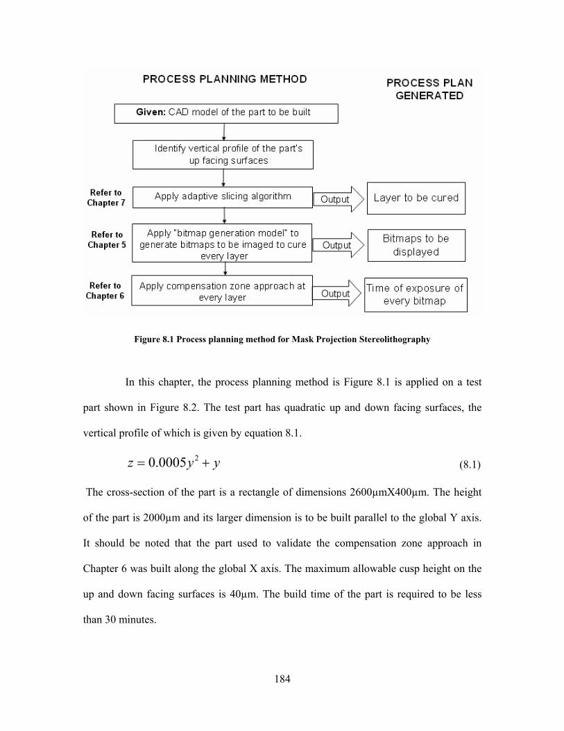
184
Figure 8.1 Process planning method for Mask Projection Stereolithography
In this chapter, the process planning method is Figure 8.1 is applied on a test
part shown in Figure 8.2. The test part has quadratic up and down facing surfaces, the
vertical profile of which is given by equation 8.1.
yyz += 20005.0 (8.1)
The cross-section of the part is a rectangle of dimensions 2600µmX400µm. The height
of the part is 2000µm and its larger dimension is to be built parallel to the global Y axis.
It should be noted that the part used to validate the compensation zone approach in
Chapter 6 was built along the global X axis. The maximum allowable cusp height on the
up and down facing surfaces is 40µm. The build time of the part is required to be less
than 30 minutes.

185
Figure 8.2 Test part to demonstrate process planning method
In Section 8.1, the test part is sliced using the adaptive slicing algorithm presented
in Chapter 7, to obtain the required tradeoff between the build time and the surface finish
of the up facing surface. One of the slicing schemes is selected for executing further steps
of process planning. The bitmaps to be imaged onto the resin surface in order to cure the
required layers are generated using the “bitmap generation model”, presented in Chapter
5. In Section 8.3, the irradiance distribution incident on the resin surface when these
bitmaps are imaged onto it is computed using the multi-scale irradiance model, presented
in Chapter 5. Using the irradiance distributions as inputs to the compensation zone
approach presented in Chapter 6, the times of exposure of these bitmaps are computed.
The part is built on the MPSLA system by using the generated process plan. The built
part is presented in Section 8.4 and its geometry is compared to the required geometry.
8.1 Slicing the part to be built
The vertical profile of the CAD model presented in Figure 8.2 is quadratic, given
by equation 8.1. The slicing algorithm for obtaining tradeoff between build time and
186
surface finish is presented in Chapter 7. As explained in Chapter 7, only the top facing
surface is of interest in executing the slicing algorithm for MPSLA, because the down-
facing surface is significantly smoother than the top-facing surface because of print
through.
The bounds on the layer thickness are taken to be 50µm to 500µm. In reality, the
MPSLA system realized as a part of this research cannot build layers thinner than 400µm.
However, purely to demonstrate the execution of the adaptive slicing algorithm, the
author has chosen the bounds on layer thicknesses to be [50µm, 500µm]. The part with
vertical dimension 2000µm can thus be meshed with a minimum of 40 layers and
maximum of 4 layers. The problem is modeled as a compromise DSP as shown in Figure
8.3.

187
Given • Part profile z = f(y): yyz += 20005.0 • Height of part 2000µm • Functions and constants related to build time Time taken to translate platform underneath recoated: Ttrans = 10s Time taken for resin to settle before exposure: TsettleK = 30000/LTk
Time of exposure for the bitmap 7.0/]5.10172.19
40[exp +
+= k
KLT
t
• Deviation variables 0;0 21 == −− dd
Find • Number of layers n • Layer thicknesses LTk • Deviation variables d1
+, d2+
Satisfy
• Sum of layer thicknesses equals part height 20001
=∑=
n
kkLT
• Bounds on layer thickness ]500,50[ mmLT µµ∈
Goals • Meet low target of surface finish
mddLT
LTfLTfLT
k
k
i
k
iii
k µ40)}])()(
(sin{tanmax[ 111
1
1
11
1 =−+−
+−=
−
=
−−
−∑ ∑
• Meet low target for build time
sddLTLTT kk
n
ksettletrans 1800)]()([ 22exp
1=−+++ +−
=∑ TT
Minimize Deviation function Example scenarios:
• Both goals rated equally: Z d d d d= + + +− + − +12
121 1 2 2( ) ( )
• Surface finish rated more than Build time: Z d d d d= + + +− + − +34
141 1 2 2( ) ( )
• Build time rated more than Surface finish: Z d d d d= + + +− + − +14
341 1 2 2( ) ( )
• Surface finish not important: Z d d d d= ⋅ + + ⋅ +− + − +0 11 1 2 2( ) ( ) • Build time not important: Z d d d d= ⋅ + + ⋅ +− + − +1 01 1 2 2( ) ( )
Figure 8.3 Modeling the slicing problem as a compromise DSP

188
Table 8.1 Optimum slicing schemes for various priorities to objectives
The cDSP presented in Figure 8.3 is executed by means of the adaptive slicing
algorithm formulated in Chapter 7 (Figure 7.11). The Matlab code written to solve the
cDSP is presented in Appendix J. The optimum slicing schemes are presented in Table
8.1.
Suppose that the process planner has the highest priority on the build time and the
least priority on the surface finish. In that case, the optimum slicing scheme will be the
one returned for the weights given to objectives on surface finish and build time as 0 and
1 respectively. Thus, the slicing scheme selected to implement the process planning
method further is the last one in Table 8.1, with all layers being 500µm.
Weights given to Surf. finish
Build time
Optimum no. of layers (n)
Layer thicknesses (µm) Objective function
(Z)
0.5 0.5 12 131.3; 139.1; 147.8; 155.9; 164.5; 172.1; 180.6; 181.7; 181.7; 181.7; 181.7; 181.7
0.8724
0.25 0.75 10 159.3; 171.4; 182.8; 194.2; 205.3; 217.4; 217.4; 217.4; 217.4; 217.4 0.4906 0.75 0.25 16 98; 103; 107.3; 111.4; 116.4; 120.9; 126.2; 129.8; 134; 136.1; 136.1;
136.1; 136.1; 136.1; 136.1; 136.1 0.8983
1 0 40 50; 50; 50; 50; 50; 50; 50; 50; 50; 50;50; 50; 50; 50; 50; 50; 50; 50; 50; 50; 50; 50; 50; 50; 50; 50; 50; 50; 50; 50; 50; 50; 50; 50; 50; 50; 50; 50; 50; 50
0
0 1 4 500; 500; 500; 500 0

189
8.2 Generating bitmaps to be imaged
Figure 8.4 Sliced part to be built
The sliced part looks as shown in Figure 8.4. It is composed of four layers, each
500µm thick and of lateral extents 2600µmX400µm. The required down facing surface is
shown by the dotted line in Figure 8.4. The four identical layers are to be cured by
imaging the same bitmap onto the resin surface. In this section, the bitmap to be imaged
onto the resin surface to cure a layer 2600µmX400µm, with its longer dimensions
parallel to global Y axis is generated.
The layer to be cured is meshed with points. These points are mapped onto the
micro-mirrors on the DMD using the “Pixel image database” (Refer to Chapter 5), in
order to determine which micro-mirrors are ‘ON’. Every ‘ON’ micro-mirror on the DMD
corresponds to a black pixel on the bitmap. The bitmap generated to cure the
2600µmX400µm layer is shown in Figure 8.5. All the black pixels in Figure 8.5
correspond to ‘ON’ micro-mirrors.

190
Figure 8.5 Bitmap generated by bitmap generation model to cure the required layer
There can be seen some jaggedness at the edges of the bitmap presented in Figure
8.5. This jaggedness is because of the errors in mapping the elements to the micro-
mirrors, as explained in Chapter 5. The white pixels dotting the edges are manually made
black and the edges are smoothened, as explained in Chapter 5, before proceeding with
the process planning method.
8.3 Applying compensation zone approach
The bitmap generated by the “bitmap generation model” is input to the multi scale
irradiance model (presented in Chapter 5) and the irradiance distribution on the resin
surface that would be made incident when the bitmap is imaged onto it is computed. The
irradiance distribution is shown in Figure 8.6.

191
Figure 8.6 Irradiance distribution along the Y dimension of the layer to be cured
In order to build the four layered part, the same bitmap as shown in Figure 8.5 is
imaged onto the resin surface. The platform is translated underneath the imaging system,
along the Y direction to offset layers over each other. The times of exposures for the
bitmaps need to be found out. This is determined by using the compensation zone
approach.
The time of exposure for the body of every layer in Figure 8.5, is imaged for 80s,
as explained in Chapter 6. We need to compute the time of exposure for the overhanging
portion of every layer. Compensation zone approach is adopted at every pixel column on
the part to be built. The generic formulation for the compensation zone approach is given
in Figure 6.14. By solving equation 6.22 at every pixel location, the times of exposure of
the overhanging region of every layer is computed. The times of exposure are shown in
Figure 8.7. The Matlab code to generate these times of exposure is presented in Appendix
J.
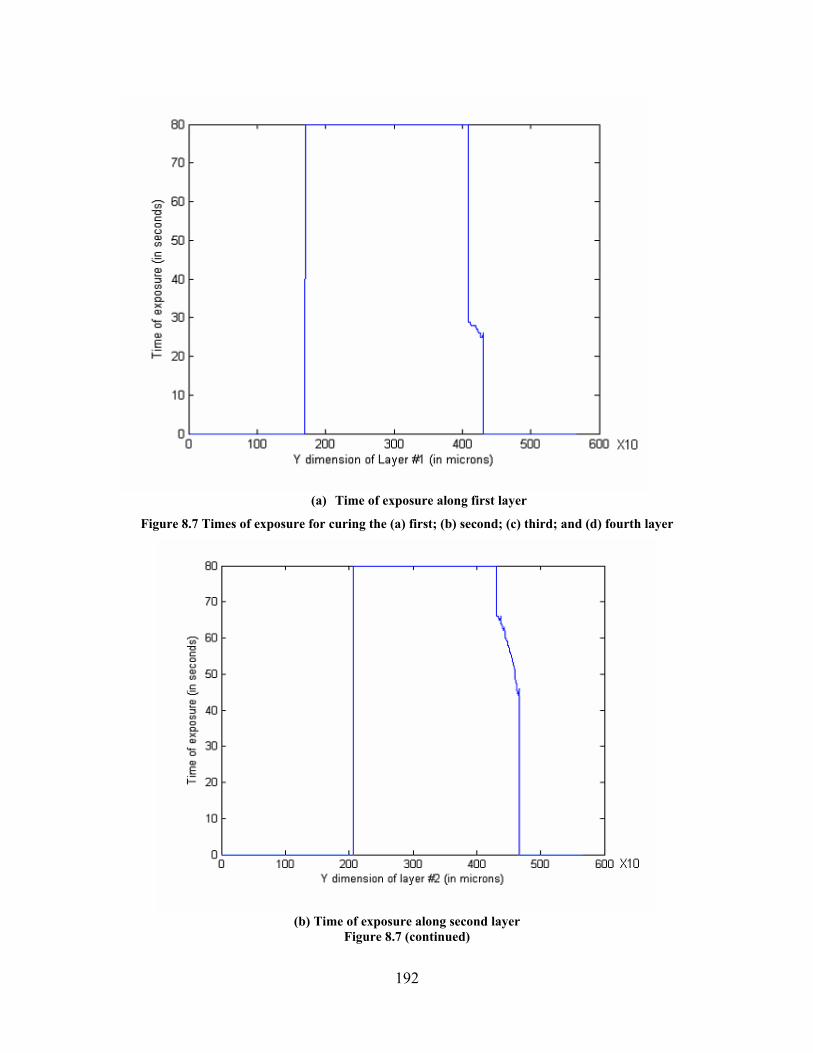
192
(a) Time of exposure along first layer
Figure 8.7 Times of exposure for curing the (a) first; (b) second; (c) third; and (d) fourth layer
(b) Time of exposure along second layer
Figure 8.7 (continued)

193
(c) Time of exposure along third layer
(d) Time of exposure along fourth layer
Figure 8.7 (continued)
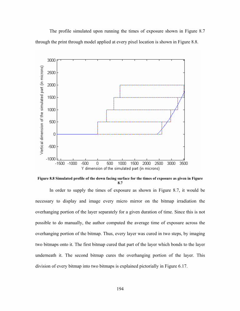
194
The profile simulated upon running the times of exposure shown in Figure 8.7
through the print through model applied at every pixel location is shown in Figure 8.8.
Figure 8.8 Simulated profile of the down facing surface for the times of exposure as given in Figure
8.7
In order to supply the times of exposure as shown in Figure 8.7, it would be
necessary to display and image every micro mirror on the bitmap irradiation the
overhanging portion of the layer separately for a given duration of time. Since this is not
possible to do manually, the author computed the average time of exposure across the
overhanging portion of the bitmap. Thus, every layer was cured in two steps, by imaging
two bitmaps onto it. The first bitmap cured that part of the layer which bonds to the layer
underneath it. The second bitmap cures the overhanging portion of the layer. This
division of every bitmap into two bitmaps is explained pictorially in Figure 6.17.
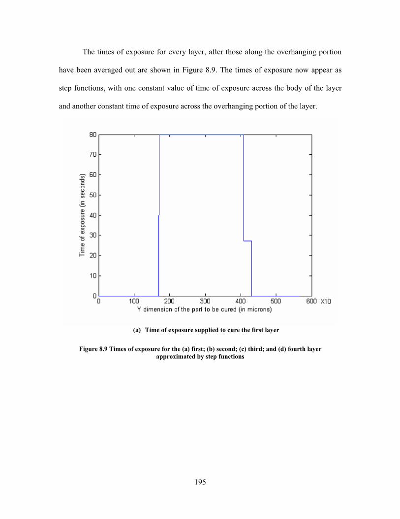
195
The times of exposure for every layer, after those along the overhanging portion
have been averaged out are shown in Figure 8.9. The times of exposure now appear as
step functions, with one constant value of time of exposure across the body of the layer
and another constant time of exposure across the overhanging portion of the layer.
(a) Time of exposure supplied to cure the first layer
Figure 8.9 Times of exposure for the (a) first; (b) second; (c) third; and (d) fourth layer approximated by step functions
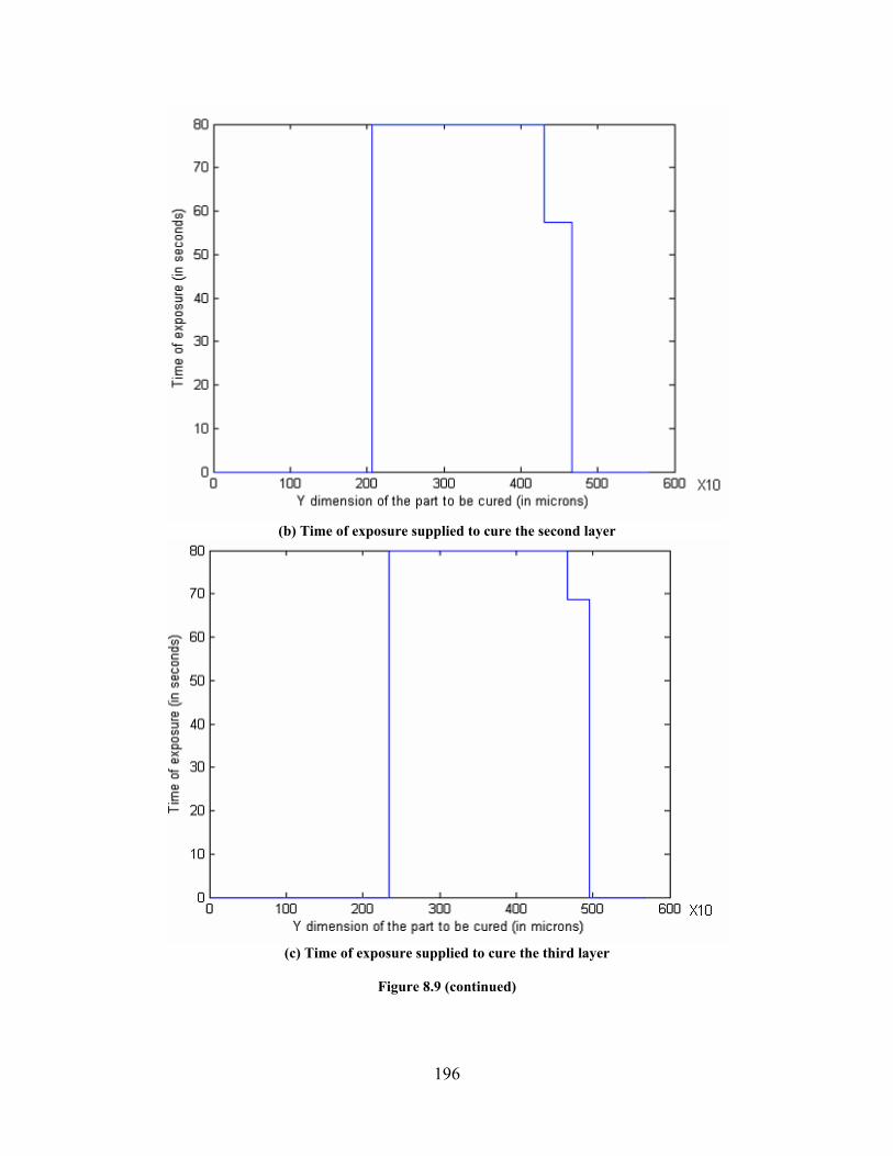
196
(b) Time of exposure supplied to cure the second layer
(c) Time of exposure supplied to cure the third layer
Figure 8.9 (continued)
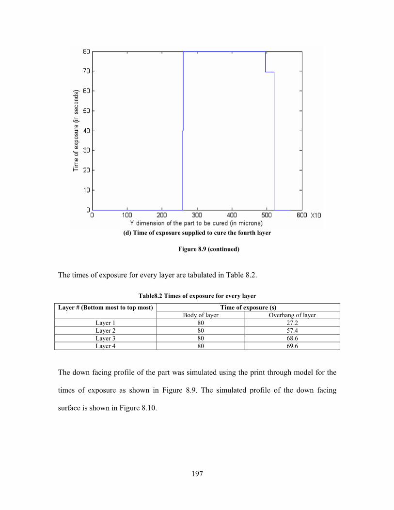
197
(d) Time of exposure supplied to cure the fourth layer
Figure 8.9 (continued)
The times of exposure for every layer are tabulated in Table 8.2.
Table8.2 Times of exposure for every layer
Time of exposure (s) Layer # (Bottom most to top most) Body of layer Overhang of layer
Layer 1 80 27.2 Layer 2 80 57.4 Layer 3 80 68.6 Layer 4 80 69.6
The down facing profile of the part was simulated using the print through model for the
times of exposure as shown in Figure 8.9. The simulated profile of the down facing
surface is shown in Figure 8.10.
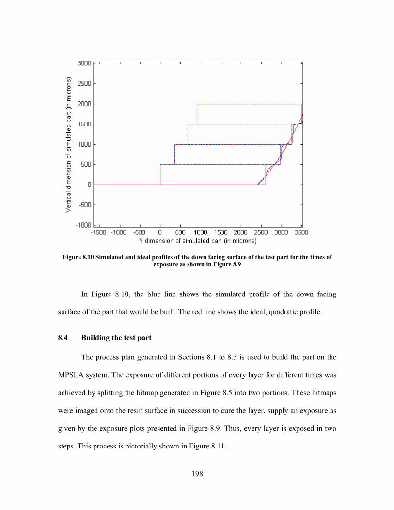
198
Figure 8.10 Simulated and ideal profiles of the down facing surface of the test part for the times of
exposure as shown in Figure 8.9
In Figure 8.10, the blue line shows the simulated profile of the down facing
surface of the part that would be built. The red line shows the ideal, quadratic profile.
8.4 Building the test part
The process plan generated in Sections 8.1 to 8.3 is used to build the part on the
MPSLA system. The exposure of different portions of every layer for different times was
achieved by splitting the bitmap generated in Figure 8.5 into two portions. These bitmaps
were imaged onto the resin surface in succession to cure the layer, supply an exposure as
given by the exposure plots presented in Figure 8.9. Thus, every layer is exposed in two
steps. This process is pictorially shown in Figure 8.11.

199
Figure 8.11 Curing every layer by imaging two bitmaps onto the resin surface in succession
The down facing profile of the part thus built is shown in Figure 8.12. In Figure 8.12, the
dotted red line is the required profile given by equation 8.1. It can be seen that the down
facing profile of the part cured approximate the required profile very well.
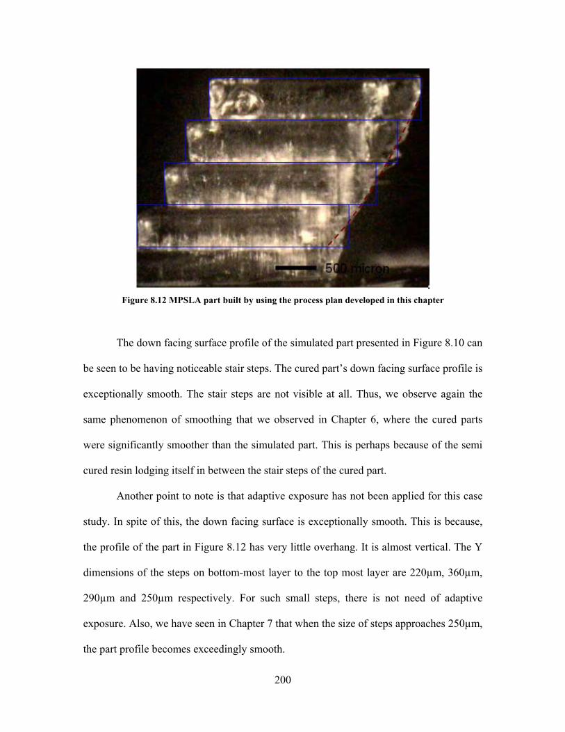
200
Figure 8.12 MPSLA part built by using the process plan developed in this chapter
The down facing surface profile of the simulated part presented in Figure 8.10 can
be seen to be having noticeable stair steps. The cured part’s down facing surface profile is
exceptionally smooth. The stair steps are not visible at all. Thus, we observe again the
same phenomenon of smoothing that we observed in Chapter 6, where the cured parts
were significantly smoother than the simulated part. This is perhaps because of the semi
cured resin lodging itself in between the stair steps of the cured part.
Another point to note is that adaptive exposure has not been applied for this case
study. In spite of this, the down facing surface is exceptionally smooth. This is because,
the profile of the part in Figure 8.12 has very little overhang. It is almost vertical. The Y
dimensions of the steps on bottom-most layer to the top most layer are 220µm, 360µm,
290µm and 250µm respectively. For such small steps, there is not need of adaptive
exposure. Also, we have seen in Chapter 7 that when the size of steps approaches 250µm,
the part profile becomes exceedingly smooth.

201
Summary
A process planning method to build a part with constraints on dimensions, surface
finish and build time is presented in Figure 8.1.The process planning method first slices
the parts using the adaptive slicing algorithm presented in Chapter 7. The sliced part is
built using Irradiance model and Compensation zone approach presented in Chapter 5
and 6 respectively. The process planning method is demonstrated on a test part with
quadratic up facing and down facing surfaces.
Progress made towards answering the research questions
Research question 4 was concerning formulating a process planning method for
MPSLA that would build a part with constraints on dimensions, surface finish and build
time. The hypothesis was that the process planning should be performed in two steps.
First, the CAD model is sliced so that the required trade off between surface finish of up
facing surface of the part to be built and the build time is obtained. In the second step, the
sliced part is to be built by using the Irradiance model and the Compensation zone
approach.
In this chapter, the process planning method is formulated and demonstrated on a
test part. The CAD model of the test part is sliced by using an adaptive slicing algorithm.
This algorithm models the trade off between the objective of surface finish of up facing
surfaces and that of build time as a compromise Decision Support Problem (cDSP). The
multi objective optimization problem is solved by using a gradient projection
optimization method. Bitmaps are generated for every layer of the sliced part using the
“Bitmap generation method” (Chapter 5) and Compensation zone approach (Chapter 7).
The part is successfully built on the MPSLA system by using the generated process plan.
202
CHAPTER 9 CLOSURE AND CONTRIBUTIONS
This chapter wraps up the dissertation. In Section 9.1, the entire work documented
in this dissertation is summarized. In Section 9.2, the research questions posed in Chapter
4 are revisited and answered by testing the proposed hypotheses. The intellectual
contributions of this work are enunciated in Section 9.3. The chapter ends with Section
9.4, which recommends the areas in which future work would be of value.
9.1 Summary of the dissertation
The objective in this research is to analyze the Mask Projection Stereolithography
(MPSLA) process in order to formulate a process planning method which would enable
the fabrication of dimensionally accurate 3D parts with constraints on build time and
surface finish. In working towards attaining this objective, a Mask Projection
Stereolithography system is designed and realized. The process of part building is
modeled and the models are validated by building test parts on the MPSLA system.
Optical models, that model the process of image formation on the resin surface when any
bitmap displayed on the mask is imaged onto it, are formulated. The process of layer
curing and the phenomenon of print through have also been modeled to understand the
sources of errors in MPSLA builds. These models have been used in a process planning
method to control the dimensional errors. The issue of obtaining a tradeoff between build
time and surface finish of MPSLA builds has also been addressed and an algorithm that
enables this tradeoff has also been presented.
Using the work presented in this dissertation, it is possible to build a MPSLA part
with multiple constraints on dimensions, surface finish and build time.
203
9.1.1 MPSLA system designed and built
A Mask Projection Stereolithography system is designed and built as a part of this
research. The design, including the bill of materials is documented in Chapter 3. A
broadband UV lamp is used as the light source. A collimating system is designed,
consisting of a pinhole and a converging lens, in order to collimate the light coming from
UV lamp. This light is made incident onto a Digital Micromirror Device (DMDTM), from
Texas InstrumentsTM, which acts as a dynamic mask. The DMDTM consists of an array of
individually addressable, bi-stable micro mirrors that can be selectively oriented to
display any bitmap (pattern). The pattern is imaged onto a photopolymer resin contained
in a vat using a 1X telecentric optical system. The optical system is designed to be
telecentric because such systems are robust against variations in image and object
distances. Layers are built on a platform which is mounted on an XYZ stage.
The MPSLA system is used to validate all the analytical models developed in this
dissertation.
9.1.2 Modeling image formation
When any bitmap displayed on the DMDTM is imaged onto the resin, an aerial
image is formed on the resin surface. This aerial image is distorted due to the optical
aberrations introduced by the imaging system and the diffraction effects. Due to these
two phenomena, the irradiance distribution across the image is also not uniform. In order
to build MPSLA parts of accurate dimensions, it is essential to model the irradiance that
any point on the resin surface would receive when any given bitmap is imaged onto it.
The modeling of image formation process has been presented in Chapter 5.

204
Two theories can be used to model image formation: the theory of physical optics,
which assumes light to be traveling in the form of wave fronts; and the theory of
geometric optics, which assumes light to be traveling as rays. The applicability of these
theories is evaluated for the imaging module of the MPSLA system assembled as a part
of this research. By performing aberration analysis, it is shown that the imaging system
realized by the author is aberration limited as opposed to diffraction limited. In case of
aberration limited optical systems, the diffraction effects are supposed to be ignored and
geometric optics give accurate results. Thus, ray tracing is used to formulate the
“Irradiance model” that models the irradiance across the resin surface, when any bitmap
is imaged onto it. The Irradiance model has been validated by building test layers on the
MPSLA system.
The Irradiance model, while high fidelity has a serious limitation, in that billions
of rays need to be traced in order to run the model. This limitation has been tackled by
adopting a multi-scale irradiance modeling strategy, in which modeling is done at two
levels: micro-mirror level and bitmap level. At the micro-mirror level, the irradiance
incident on the resin surface when every micro-mirror is individually imaged onto it is
recorded and stored in a database. At the bitmap level, the irradiance distributions
corresponding to all the ‘ON’ micro mirrors are mined from the database and combined
to obtain the irradiance distribution on the resin surface when that bitmap is imaged onto
it. This modeling strategy resulted in reduction in the computation time by a factor of
1/600.

205
9.1.3 Cure modeling
In Chapter 6, cure modeling is done at two levels. First, the thickness of the layer
that would be cured when any bitmap is imaged onto the resin surface is modeled.
Second, the print through that would result when multiple layers are cured over each
other is modeled.
In Chapter 6, the transient model of layer curing is presented. This model takes
into account the change in the rate of attenuation of light in the resin during exposure. It
has been shown that, for large exposure times, cure depth is a linear function of exposure
as opposed to being a logarithmic function. The transient layer cure model has been
validated by building test layers on the MPSLA system.
The effect of diffusion of reactive species away from the bottom surface of a part
being built has been quantified. When a MPSLA part is being built, reactive species are
present at the bottom surface of the part, near the solid-liquid interface. These reactive
species, in their excited state, carry a total energy equal to the threshold exposure of
polymerization (Ec). When the part sits in the resin vat, these reactive species diffuse out
carrying energy away with them. Also, oxygen from surrounding resin diffuses in and
‘quenches’ the excited species. Due to this, the effective exposure at the bottom surface
of an MPSLA part drops down as a function of time. The rate of drop of effective
exposure has been quantified in Chapter 6.
Chapter 6 also presents the “print through model”, which computes the amount of
print through that would occur when a multi-layered part is built. Print through is caused
due to residual radiation penetrating beyond the intended layer thickness to the bottom
surface of part, causing unwanted curing. The print through model is used to simulate the

206
profile of the down facing surface of a test four-layered part. The simulation is validated
by building test parts on the MPSLA system.
The print through model is used to formulate the “compensation zone approach”,
which is essentially, the inverse of the print through model. The compensation zone
approach enables the computation of process parameters that would result a part with the
required down facing profile. The compensation zone approach is demonstrated
successfully on a test part.
9.1.4 Improving surface finish of MPSLA builds
The compensation zone approach presented in Chapter 6 is validated by exposing
the overhanging portion of a layer for time duration different from the duration time that
its body was exposed. The method of adaptive exposure was proposed in Chapter 7. This
method entailed discretizing the overhanging portion of every layer even more in order to
better approximate the down-facing profile. This method was demonstrated on a test part.
The slicing of an MPSLA part influences its build time as well as its surface
finish. Larger layer thicknesses result in shorter build times but poor surface finish, while
smaller layer thicknesses result in smoother surfaces, but larger build times. It is essential
to select a slicing scheme that would achieve a tradeoff between these two objectives.
A multi-objective slicing algorithm is formulated and demonstrated on a quadratic
down facing surface in Chapter 7.
207
9.2 Revisiting the research questions
In this section, the research questions posed in Chapter 4 are revisited and the
proposed hypotheses tested. The purpose of this research was to achieve the objective
presented in Chapter 1, restated here:
“To formulate a process planning method to build MPSLA parts with
constraints on dimensions, surface finish and build time”
This objective is broken down in Chapter 4 and research question and hypothesis are
proposed for each of them. In light of the work presented in this thesis, the validity of
these hypotheses is tested in this section.
Research Question 1a: Should the image formation process in the MPSLA system under
consideration by modeled using physical optics or using geometric optics?
Hypothesis: The theory of geometric optics is more suitable than that of physical optics
to model the image formation by the MPSLA system under consideration.
Testing the hypothesis: It has been determined from literature in optics that the Optical
Path Difference (OPD) is the measure of the wave front aberrations and can be used as a
guideline to choose the optical modeling method. The OPD of the imaging system of the
MPSLA system was computed by modeled the system using the optical analysis software
OSLOTM to show that the imaging system is aberration limited.
The irradiance is modeled using ray-tracing algorithm as the “Irradiance model”.
This is the method of modeling an aberration limited optical system. The Irradiance
model is validated by curing test layers on the MPSLA system. The close agreement in
the dimensions of the cured layers and the dimensions of the aerial image formed on the

208
resin, computed by the Irradiance model, suggests that the Irradiance model is valid.
Thus, the geometric optics has been used successfully to model the image formation
process for the MPSLA system. Thus, the hypothesis has been tested and has been found
to be valid.
Research Question 1b: How to model the exposure profile on the resin surface with the
fidelity of the ray tracing approach, in a computationally inexpensive way?
Hypothesis: A multi scale modeling approach can be adopted. The irradiance profile can
be thought of as a collection of pixels overlapping each other. Modeling should be done
at two levels:
1. Curing of individual pixels (computationally expensive part)
2. Overlapping of pixels to give the exposure profile on the resin surface
(computationally inexpensive part)
Testing the hypothesis: The “Pixel image model” has been formulated in Chapter 5.
This models the irradiance on the resin surface when every micro-mirror is imaged
individually onto it. The irradiance is stored as a matrix. This database is used to model
the irradiance on the resin surface when a test bitmap was imaged onto it. The
computation of the irradiance entailed simply choosing the pixels (irradiance matrices)
corresponding to the ‘ON’ micro mirrors from the Pixel image database, and adding them
up. The time to compute the irradiance computation created by a test bitmap without
using the pixel image database was found to be 152 hours. Using the Pixel image
database, the same irradiance distribution could be generated in less than 15 minutes.

209
Thus, the multi-scale modeling approach resulted in significant savings in the
computation time. Thus validates the hypothesis to research question 1b.
Research Question 2: How to reduce print through errors in MPSLA builds?
Hypothesis: Print through errors can be reduced by subtracting a tailored volume
(compensation zone) from underneath the CAD model which is used to build the part, in
such a way that the exposure received by the down facing surface of the part is exactly
equal to the threshold exposure of polymerization (Ec).
This research question was further broken down into two sub-questions in the
course of this research. We test the hypotheses to these sub-research questions before
testing the hypothesis to research questions 2.
Research Question 2a: How to capture the effect of the varying rate of radiation
attenuation throughout the duration of exposure, as a layer gets cured?
Hypothesis: The effect of varying rate of attenuation as a layer gets cured can be
captured by modeling layer curing as a transient phenomenon, by discretizing the time
domain.
Testing the hypothesis: In Chapter 6, the incremental curing that would occur during an
infinitesimal duration of time is modeled as a differential equation. This equation takes
into account the different rate of attenuation through a cured layer and the uncured resin
underneath that layer. The differential equation is solved numerically to obtain an almost
linear relationship between cure depth and exposure. This linear relationship is validated
by building test layers on the MPSLA system. The values of the constants of this linear

210
curve between cure depth and exposure are determined experimentally. Thus, layer
curing has been successfully modeled as a transient process and this model has been
validated. This successfully tests the hypothesis to research question 2a.
Research Question 2b: Is exposure at the bottom surface of a cured layer additive or
does it get significantly affected by diffusion of radicals and oxygen into the resin vat?
Hypothesis: The exposure is not additive because there is a significant diffusion of
radicals and oxygen in the resin vat.
Testing of hypothesis: The loss energy due to diffusion of radicals and oxygen
underneath the bottom surface of a cured layer is assumed to be a factor k times the
energy at the bottom surface of the layer when it was just cured (Ec). Layers were cured
using two discrete exposure doses and allowing the layer to stay in the resin for a variable
duration of time in between these two exposure doses. The value of ‘k’ was found out by
measuring the thickness of the layer cured after receiving both the exposure doses. The
relationship between k and the time that the layer was allowed to stay in the resin in
between the two exposures was found to be logarithmic. Thus, the loss of energy from
underneath the bottom of a cured layer varies as the logarithm of time. This is typical of
the diffusion phenomenon. This lends strong evidence that there is a loss of effective
exposure from the bottom surface of a part being built due to a diffusion based
phenomenon (most likely the diffusion of reactive species and oxygen molecules) thereby
making the additive nature of exposure a strong function of time.
Now, we can revisit the hypothesis to research question 2. In Chapter 6, the “Print
through model is formulated using the models developed in testing hypotheses 2a and 2b.

211
The print through model computes the print through that would occur underneath a multi-
layered MPSLA build. This model is used to compute the reduced time of exposure for
which the lower most layers of an MPSLA build must be exposed. When the lower most
layer is exposed for a lesser duration of time, the effect is the same as subtracting a
tailored volume from underneath the CAD model to be built. The compensation zone
approach has been demonstrated on a test part.
Research question 3: How to implement the print through smoothing approach to obtain
smoother down facing surfaces in MPSLA builds?
Hypothesis: Print through smoothing can be achieved by gray scaling the pixels near the
edges of a layer to cure voxels of different heights that conform to the part’s vertical
profile. This method shall be called as “adaptive exposure” since it involves adapting the
exposure to suit the part’s vertical profile.
Testing the hypothesis: The adaptive exposure method entails modulating the exposure
at the edges of the layers in such a way that profile of the edges confirm to the part’s
down facing vertical profile. This method has been demonstrated in Chapter 7. Exposure
has been modulated at the edges by using three bitmaps to cure every layer. The
improvement in surface finish is demonstrated by building a part without adaptive
exposure (Chapter 6) and with adaptive exposure (Chapter 7).
Research Question 4: How to build a MPSLA part with multiple objectives of
dimensional accuracy, surface finish and build time?

212
Hypothesis: Process planning can be done in two steps. First, a multi-objective
optimization method, like the compromise DSP (Mistree et al., 1994) should be
formulated and solved to select the slicing scheme, i.e. layer thicknesses that would
obtain a tradeoff between the objectives of surface finish and build time. For this slicing
scheme, the compensation zone approach should be adopted to obtain part with accurate
vertical dimensions
Testing the hypothesis: The process planning method to build a MPSLA part with
constraints on dimensions, surface finish and build time is presented in Figure 8.1. The
process planning method first slices the CAD model to be built by adopting the adaptive
slicing algorithm presented in Chapter 7. The compensation zone approach (Chapter 6)
and Irradiance model (Chapter 5) is then used to build the sliced part. The process
planning method is demonstrated on a part with quadratic up- and down facing surfaces
in Chapter 8.
9.3 Contributions
The contributions made by this work can be characterized into two categories:
1. Contributions to fundamental knowledge in Stereolithography; and
2. Developmental contributions
9.3.1 Contribution to fundamental knowledge
Process planning literature available for the conventional laser scanning
Stereolithography allows a manufacturer to build prototypes with the required properties.
This literature can’t be directly extended to Mask Projection micro Stereolithography
because the nature of irradiation of the resin surface and curing characteristics of a resin
213
are considerably different in both the cases. The primary contributions of this work are in
the realm of analyzing the MPµSLA process and explaining it in mathematical terms.
The following are the contributions of the thesis to the field of MPµSLA:
The irradiation of the resin surface in the case of MPµSLA is a much more
complex process than that achieved by laser scanning. While the laser beam has a
Gaussian irradiance profile, which remains constant regardless of the cross section it is
scanning, in case of MPµSLA, the irradiation distribution changes with the change in the
pattern imaged. The method of modeling irradiance on the resin surface in a
computationally feasible manner is the first contribution on this work.
The transient model is more rigorous than the conventional Stereolithography
cure model, which assumes that the entire energy is delivered to the resin in one instant
and that the light gets attenuated exponentially according to the Beer Lambert’s law. The
transient model takes into account the variation in the rate of attenuation of light during
exposure. This model has been formulated and validated on the MPSLA system.
The effect of diffusion of reactive species away from, and oxygen towards, the
bottom surface of a part being built has also been quantified for the first time (radical
diffusion model). Standard Stereolithography texts ignore these diffusion phenomena and
treat exposure to be additive. The author has shown that there is a fall in the energy at the
bottom surface of a MPSLA part being built due to diffusion and has quantified the rate
of loss of this energy.
The transient layer cure model and the radical diffusion model have been used to
model the print through that would result when a multi layered part is built. This model is
used to formulate the compensation zone approach, which enables the avoiding of print

214
through errors. The compensation zone approach, which deals with the tailoring of
process parameters in order to avoid print through errors, is also presented for the first
time in Stereolithography literature.
It is for the first time that print through smoothing has been demonstrated to
approximate the vertical profile of the part, by adaptive exposure.
9.3.2 Developmental contributions
Apart from the intellectual contributions, there are a number of contributions of a
developmental nature. An MPSLA system has been successfully realized. The design of
the system has been documented, which will enable replication of this system.
A slicing algorithm that computes the optimum slicing scheme that achieves a
tradeoff between build time and surface finish has been formulated. This algorithm can
be used not just for Stereolithography, but also for any additive manufacturing process.
A process planning method that would guide a manufacturer through all steps of
process planning, starting from the CAD model and ending with a finished part has been
formulated.
9.4 Future work
Future work is needed from the view of bolstering confidence in the models and
process planning methods presented in this thesis.
The transient layer cure model developed in Chapter 6 predicts a linear
relationship between cure depth and exposure, for long durations of exposure. This model
has been validated by building layers in the DSM SOMOS 10120TM resin. It will be
useful to validate this model on other resins.

215
The MPSLA system could repeatedly lay down layers only as thick as 500µm.
Layers thinner than that could not be laid down with confidence. As a result, all the multi
layered parts built presented in this dissertation have been built using 500µm thick layers.
It would be useful to validate the compensation zone approach for layers of thicknesses
smaller than 500µm. It should be noted that the compensation zone approach is based
upon the transient layer cure model and the diffusion mode, both of which have been
validated for cure depths starting at around 70µm. So, the compensation zone approach is
definitely expected to work well at smaller layer thicknesses, even though an actual
demonstration would increase confidence in it.
All the multi layered parts cured have been observed to be significantly smoother
down facing surface than those predicted by the simulations. The author surmises that the
smoothing is because of partially cured resin lodging itself between the stair steps. This
claim however has not been validated. It would be of value of conclusively explain the
cause behind the smoothing of down facing surfaces.
Future work is needed towards improving the MPSLA system. The imaging
module of the current MPSLA system is severely aberration limited. This limits the size
of the bitmap that can be imaged onto the resin surface within reasonable distortions. The
imaging system can be made more sophisticated by introducing more number of optical
components, so that aberrations can be reduced and the field of exposure can be
increased.
The author has used a commercial Stereolithography resin (DSM SOMOS 10120)
with his system. This resin has a very high value of depth of penetration (Dp), i.e. very
low rate of attenuation of radiation. For micro applications, a resin which would result in

216
rapid attenuation of radiation, and hence thinner layer should be used. Another limitation
of using DSM SOMOS 10120 is its high viscosity (120 cP). This high viscosity prohibits
laying down of very thin films of resin. A resin with lower viscosity would enable laying
down of much thinner layers.

217
APPENDIX A. VALIDATION OF IRRADIANCE MODEL
In this appendix, the test layers cured to validate the irradiance model formulated
in Chapter 5 are presented. In all, eight cross shaped layers were cured by imaging a test
bitmap onto the resin surface. The dimensions of these layers were measured and
compared with the dimensions of the irradiance profile returned by the irradiance model.
The dimensions of the layers are recorded in Table 5.1.
Figure A. 1 Validating irradiance model: Test layer 1

218
Figure A. 2 Validating irradiance model: Test layer 2

219
Figure A. 3 Validating irradiance model: Test layer 3
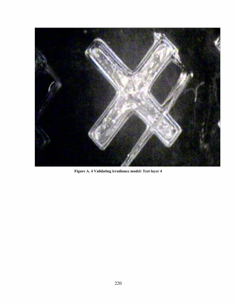
220
Figure A. 4 Validating irradiance model: Test layer 4

221
Figure A. 5 Validating irradiance model: Test layer 5

222
Figure A. 6 Validating irradiance model: Test layer 6

223
Figure A. 7 Validating irradiance model: Test layer 7

224
Figure A. 8 Calibration scale for measuring the dimensions of the test layers

225
Figure A. 9 Validating irradiance model: Test layer 8
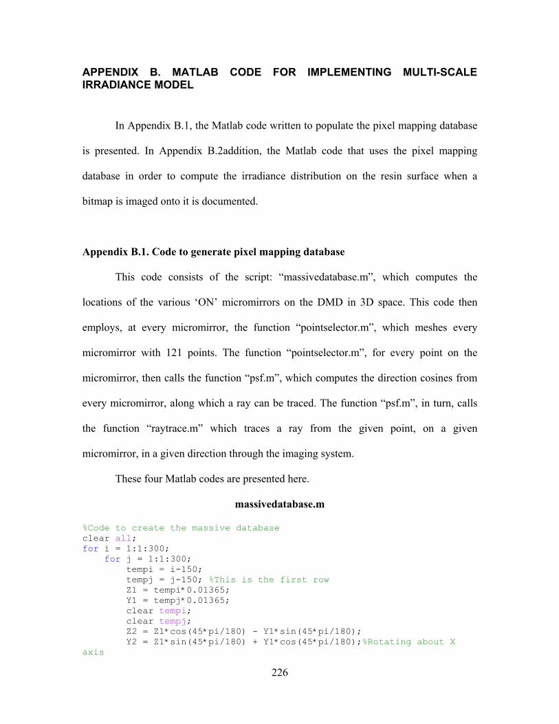
226
APPENDIX B. MATLAB CODE FOR IMPLEMENTING MULTI-SCALE IRRADIANCE MODEL
In Appendix B.1, the Matlab code written to populate the pixel mapping database
is presented. In Appendix B.2addition, the Matlab code that uses the pixel mapping
database in order to compute the irradiance distribution on the resin surface when a
bitmap is imaged onto it is documented.
Appendix B.1. Code to generate pixel mapping database
This code consists of the script: “massivedatabase.m”, which computes the
locations of the various ‘ON’ micromirrors on the DMD in 3D space. This code then
employs, at every micromirror, the function “pointselector.m”, which meshes every
micromirror with 121 points. The function “pointselector.m”, for every point on the
micromirror, then calls the function “psf.m”, which computes the direction cosines from
every micromirror, along which a ray can be traced. The function “psf.m”, in turn, calls
the function “raytrace.m” which traces a ray from the given point, on a given
micromirror, in a given direction through the imaging system.
These four Matlab codes are presented here.
massivedatabase.m
%Code to create the massive database clear all; for i = 1:1:300; for j = 1:1:300; tempi = i-150; tempj = j-150; %This is the first row Z1 = tempi*0.01365; Y1 = tempj*0.01365; clear tempi; clear tempj; Z2 = Z1*cos(45*pi/180) - Y1*sin(45*pi/180); Y2 = Z1*sin(45*pi/180) + Y1*cos(45*pi/180);%Rotating about X axis
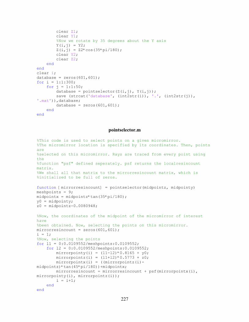
227
clear Z1; clear Y1; %Now we rotate by 35 degrees about the Y axis Y(i,j) = Y2; Z(i,j) = Z2*cos(35*pi/180); clear Y2; clear Z2; end end clear i; database = zeros(601,601); for i = 1:1:300; for j = 1:1:50; database = pointselector(Z(i,j), Y(i,j)); save (strcat('database', (int2str(i)), '.', (int2str(j)), '.mat')),database; database = zeros(601,601); end end
pointselector.m
%This code is used to select points on a given micromirror. %The micromirror location is specified by its coordinates. Then, points are %selected on this micromirror. Rays are traced from every point using the %function "psf" defined seperately. psf returns the localresincount matrix. %We shall all that matrix to the mirrorresincount matrix, which is %initialized to be full of zeros. function [mirrorresincount] = pointselector(midpointz, midpointy) meshpoints = 9; midpointx = midpointz*tan(35*pi/180); y0 = midpointy; z0 = midpointz-0.0080948; %Now, the coordinates of the midpoint of the micromirror of interest have %been obtained. Now, selecting the points on this micromirror. mirrorresincount = zeros(601,601); i = 1; %Now, selecting the points for l1 = 0:0.0109552/meshpoints:0.0109552; for l2 = 0:0.0109552/meshpoints:0.0109552; mirrorpointy(i) = (l1-l2)*0.8165 + y0; mirrorpointz(i) = (l1+l2)*0.5773 + z0; mirrorpointx(i) = ((mirrorpointz(i)-midpointz)*tan(45*pi/180))+midpointx; mirrorresincount = mirrorresincount + psf(mirrorpointx(i), mirrorpointy(i), mirrorpointz(i)); i = i+1; end end

228
psf.m
%Code written to compute the Point Spread Function (PSF) %Code will trace rays from one point through the tleecentric imagign %system. Rays are emitted in a cone. It is assumed that all these rays have %the same amount if energy. The cone angle is the variable. %This code uses the function "raytrace" to trace rays from a given point in a given direction. "Raytrace" which is defined seperately. %************************************************************************** %The number of rays from the point (pointx,pointy,pointz) hitting every %small square in the resindatabase is counted and stored in the counter %localraycount(y,z). %For example, localraycount(1,1) will denote the square centered at (-4.5,-4.5). %localresincount, because it is going to measure only the rays in this %function. Later the contents of local raycount will be transferred to the %matrix resincount, which shall be in the code that selects points on the %micromirror. function[localresincount] = psf(pointx,pointy,pointz); %Start point is 0,0,0 raycount = 1; pupildistance = 100; %Entrance pupil at 100mm from start point theta = 1.5; %Half angle of cone. Makes pupil radius = 5mm pupilradius = pupildistance*theta*pi/180; for i = -pupilradius:pupilradius/15:pupilradius; for j = -pupilradius:pupilradius/15:pupilradius; if sqrt(i^2+j^2) <= pupilradius; Y(raycount) = (pointy-i)/sqrt((i-pointy)^2+(j-pointz)^2+(pupildistance-pointx)^2); Z(raycount) = (pointz-j)/sqrt((i-pointy)^2+(j-pointz)^2+(pupildistance-pointx)^2); X(raycount) = (pupildistance-pointx)/sqrt((i-pointy)^2+(j-pointz)^2+(pupildistance-pointx)^2); check(raycount) = Y(raycount)*Y(raycount)+Z(raycount)*Z(raycount)+X(raycount)*X(raycount); [resiny(raycount), resinz(raycount)] = raytrace(pointx, pointy, pointz, X(raycount), Y(raycount), Z(raycount)); phi(raycount) = atan((sqrt(i^2+j^2))/pupildistance); weight(raycount) = 1*cos(phi(raycount))*cos(phi(raycount)); if resiny(raycount) == 1000; raycount = raycount - 1; end raycount = raycount + 1; end

229
end end sizey = max(size(resiny)); if sizey == raycount resiny(raycount) = []; resinz(raycount) = []; weight(raycount) = []; end clear i; clear j; %Now, we count the rays in the tiny squares that the resin surface is %discretized into. The squares are 10 micron each. The extents of the %resin are from -3 to +3 mm. The number of divisions will be (6/0.01 + 1) = 601 localresincount = zeros(601,601); for i = 1:1:sizey-1; localy = int16(((resiny(i)+3)/0.01))+1; localz = int16(((resinz(i)+3)/0.01))+1; localresincount(localz,localy) = localresincount(localz,localy)+1; end
raytrace.m
%Function to trace a single ray from a given point in a given direction %Written by Ameya Limaye on May 19 2006 function[y6,z6]= raytrace(x1,y1,z1,X1,Y1,Z1) x(1) = x1; y(1) = y1; z(1) = z1; X(1) = X1; Y(1) = Y1; Z(1) = Z1; %Inputting the system parameters c(1) = 0; % c is the curvature of surface c(2) = 0.028; c(3) = -0.028; c(4) = 0.028; c(5) = -0.028; c(6) = 0; t(1) = 36.65-x1; %t is the distance t(2) = 6.7; t(3) = 73.3; t(4) = 6.7; t(5) = 36.65; N(1) = 1; %N is the refractive index N(2) = 1.46; N(3) = 1; N(4) = 1.46; N(5) = 1; aperture = 1; %Aperture stop = 2mm radius

230
%Now, tracing the ray from x1,y1,z1 in direction X1, Y1, Z1 i = 2; %Transfer equations e(i) = t(i-1)*X(i-1) - (x(i-1)*X(i-1) + y(i-1)*Y(i-1) + z(i-1)*Z(i-1)); Mx(i) = x(i-1) + e(i)*X(i-1) - t(i-1); Msquare(i) = x(i-1)^2 + y(i-1)^2 + z(i-1)^2 - e(i)^2 + t(i-1)^2 - 2*t(i-1)*x(i-1); E(i) = sqrt(X(i-1)^2 - c(i)*(c(i)*Msquare(i) - 2*Mx(i))); L(i) = e(i) + (c(i)*Msquare(i) - 2*Mx(i))/(X(i-1)+E(i)); x(i) = x(i-1) + L(i)*X(i-1) - t(i-1); y(i) = y(i-1) + L(i)*Y(i-1); z(i) = z(i-1) + L(i)*Z(i-1); %Refarction equations Edash(i) = sqrt(1- ((N(i-1)/N(i))^2) * (1-E(i)^2)); g(i) = Edash(i) - ((N(i-1)/N(i)))*E(i); X(i) = (N(i-1)/N(i))*X(i-1) - g(i)*c(i)*x(i) + g(i); Y(i) = (N(i-1)/N(i))*Y(i-1) - g(i)*c(i)*y(i); Z(i) = (N(i-1)/N(i))*Z(i-1) - g(i)*c(i)*z(i); clear i; i = 3; %Transfer equations e(i) = t(i-1)*X(i-1) - (x(i-1)*X(i-1) + y(i-1)*Y(i-1) + z(i-1)*Z(i-1)); Mx(i) = x(i-1) + e(i)*X(i-1) - t(i-1); Msquare(i) = x(i-1)^2 + y(i-1)^2 + z(i-1)^2 - e(i)^2 + t(i-1)^2 - 2*t(i-1)*x(i-1); E(i) = sqrt(X(i-1)^2 - c(i)*(c(i)*Msquare(i) - 2*Mx(i))); L(i) = e(i) + (c(i)*Msquare(i) - 2*Mx(i))/(X(i-1)+E(i)); x(i) = x(i-1) + L(i)*X(i-1) - t(i-1); y(i) = y(i-1) + L(i)*Y(i-1); z(i) = z(i-1) + L(i)*Z(i-1); %Refarction equations Edash(i) = sqrt(1- ((N(i-1)/N(i))^2) * (1-E(i)^2)); g(i) = Edash(i) - ((N(i-1)/N(i)))*E(i); X(i) = (N(i-1)/N(i))*X(i-1) - g(i)*c(i)*x(i) + g(i); Y(i) = (N(i-1)/N(i))*Y(i-1) - g(i)*c(i)*y(i); Z(i) = (N(i-1)/N(i))*Z(i-1) - g(i)*c(i)*z(i); clear i; i = 4; %Transfer equations e(i) = t(i-1)*X(i-1) - (x(i-1)*X(i-1) + y(i-1)*Y(i-1) + z(i-1)*Z(i-1)); Mx(i) = x(i-1) + e(i)*X(i-1) - t(i-1); Msquare(i) = x(i-1)^2 + y(i-1)^2 + z(i-1)^2 - e(i)^2 + t(i-1)^2 - 2*t(i-1)*x(i-1); E(i) = sqrt(X(i-1)^2 - c(i)*(c(i)*Msquare(i) - 2*Mx(i))); L(i) = e(i) + (c(i)*Msquare(i) - 2*Mx(i))/(X(i-1)+E(i)); x(i) = x(i-1) + L(i)*X(i-1) - t(i-1);

231
y(i) = y(i-1) + L(i)*Y(i-1); z(i) = z(i-1) + L(i)*Z(i-1); %Refarction equations Edash(i) = sqrt(1- ((N(i-1)/N(i))^2) * (1-E(i)^2)); g(i) = Edash(i) - ((N(i-1)/N(i)))*E(i); X(i) = (N(i-1)/N(i))*X(i-1) - g(i)*c(i)*x(i) + g(i); Y(i) = (N(i-1)/N(i))*Y(i-1) - g(i)*c(i)*y(i); Z(i) = (N(i-1)/N(i))*Z(i-1) - g(i)*c(i)*z(i); %Check if the ray passes through the aperture stop if (((y(3)+y(4))/2)^2 + ((z(3)+z(4))/2)^2)<= aperture^2 clear i; i = 5; %Transfer equations e(i) = t(i-1)*X(i-1) - (x(i-1)*X(i-1) + y(i-1)*Y(i-1) + z(i-1)*Z(i-1)); Mx(i) = x(i-1) + e(i)*X(i-1) - t(i-1); Msquare(i) = x(i-1)^2 + y(i-1)^2 + z(i-1)^2 - e(i)^2 + t(i-1)^2 - 2*t(i-1)*x(i-1); E(i) = sqrt(X(i-1)^2 - c(i)*(c(i)*Msquare(i) - 2*Mx(i))); L(i) = e(i) + (c(i)*Msquare(i) - 2*Mx(i))/(X(i-1)+E(i)); x(i) = x(i-1) + L(i)*X(i-1) - t(i-1); y(i) = y(i-1) + L(i)*Y(i-1); z(i) = z(i-1) + L(i)*Z(i-1); %Refarction equations Edash(i) = sqrt(1- ((N(i-1)/N(i))^2) * (1-E(i)^2)); g(i) = Edash(i) - ((N(i-1)/N(i)))*E(i); X(i) = (N(i-1)/N(i))*X(i-1) - g(i)*c(i)*x(i) + g(i); Y(i) = (N(i-1)/N(i))*Y(i-1) - g(i)*c(i)*y(i); Z(i) = (N(i-1)/N(i))*Z(i-1) - g(i)*c(i)*z(i); clear i; i = 6; %Transfer equations e(i) = t(i-1)*X(i-1) - (x(i-1)*X(i-1) + y(i-1)*Y(i-1) + z(i-1)*Z(i-1)); Mx(i) = x(i-1) + e(i)*X(i-1) - t(i-1); Msquare(i) = x(i-1)^2 + y(i-1)^2 + z(i-1)^2 - e(i)^2 + t(i-1)^2 - 2*t(i-1)*x(i-1); E(i) = sqrt(X(i-1)^2 - c(i)*(c(i)*Msquare(i) - 2*Mx(i))); L(i) = e(i) + (c(i)*Msquare(i) - 2*Mx(i))/(X(i-1)+E(i)); x(i) = x(i-1) + L(i)*X(i-1) - t(i-1); y(i) = y(i-1) + L(i)*Y(i-1); z(i) = z(i-1) + L(i)*Z(i-1); x6 = x(6); y6 = y(6); z6 = z(6); else x6 = 1000; y6 = 1000; z6 = 1000; end

232
clear i;
Appendix B.2. Code to use generate pixel mapping to compute irradiance distribution
The name of the Matlab code which computes the irradiance distribution using the
pixel-mapping database is “bitmap_read_database.m”. This code takes in the bitmap as
an input and mines the irradiance distribution corresponding to every black, i.e. ‘ON’
pixel. These irradiance distributions are added together to obtain the irradiance
distribution.
bitmap_read_database.m
%This is the code to get a bitmap and then use the Pixel Image Database to %populated the irradiance distribution. %Code written by Ameya on April 29th clear all; bitmap_matrix = imread('C:\Ameya\JournalPaper3\Generating bitmaps\layer_bitmap_GT.bmp','BMP'); irradiance_body = zeros(601,601); for i = 1:1:300 for j = 1:1:100 if bitmap_matrix(i,j) == 0 load (strcat('Database300.1to100\database', (int2str(i)), '.', (int2str(j)), '.mat')) irradiance_body = irradiance_body + database; clear database; clear Z; clear Y; end end end for i = 1:1:300 for j = 101:1:200 if (bitmap_matrix(i,j) == 0) load (strcat('Database300.101to200\database', (int2str(i)), '.', (int2str(j)), '.mat')) irradiance_body = irradiance_body + database; clear database; clear Z; clear Y; end

233
end end for i = 1:1:300 for j = 201:1:300 if bitmap_matrix(i,j) == 0 load (strcat('Database300.201to300\database', (int2str(i)), '.', (int2str(j)), '.mat')) irradiance_body = irradiance_body + database; clear database; clear Z; clear Y; end end end for i = 1:1:601; for j = 1:1:601; for k = 1:1:2; B(i,j,k) = irradiance_body(i,j); end end end A = smooth3(smooth3(B)); irradiance = A(:,:,1); for i = 1:1:601; X(i) = 10*i-10; end factor = 0.7/max(max(irradiance)); irradiance = irradiance*factor; plot(X,max(irradiance)); AMEYA = 100 clear bitmap_matrix irradiance_strip = zeros(601,601); bitmap_matrix = imread('C:\Ameya\JournalPaper3\4 layer linear part 500 layer thick_ AT EDGE\strip1.bmp','BMP'); for i = 1:1:300 for j = 1:1:100 if bitmap_matrix(i,j) == 0 load (strcat('Database300.1to100\database', (int2str(i)), '.', (int2str(j)), '.mat')) irradiance_strip = irradiance_strip + database; clear database; clear Z; clear Y; end end end

234
for i = 1:1:300 for j = 101:1:200 if bitmap_matrix(i,j) == 0 load (strcat('Database300.101to200\database', (int2str(i)), '.', (int2str(j)), '.mat')) irradiance_strip = irradiance_strip + database; clear database; clear Z; clear Y; end end end for i = 1:1:300 for j = 201:1:300 if bitmap_matrix(i,j) == 0 load (strcat('Database300.201to300\database', (int2str(i)), '.', (int2str(j)), '.mat')) irradiance_strip = irradiance_strip + database; clear database; clear Z; clear Y; end end end

235
APPENDIX C. MATLAB CODE TO IMPLEMENT INVERSE IRRADIANCE MODEL
In this Appendix, the Matlab code “element_micromirror_mapping” is presented.
This code meshes the layer to be cured with 10µmX10µm squares. Then, for every
element that is at the center of any pixel in the pixel-mapping-database, it designates the
corresponding micro-mirror on the DMD ‘ON’. Once the micro-mirrors to be turned
‘ON’ are known, the bitmap is generated by making every corresponding pixel black.
element_micromirror_mapping.m
%Code to map the a layer ont oa bitmap using the lement database %Code writen by Ameya on 3rh May %****************************% %This code takes in an element. Then, it sees if it is at the center of any %micromirror. It goes to every micromirror and sees inf the element of %interest is at its center. Very long, inefficient algorithm:( clear all load 'elements.mat' bitmap_matrix = imread('strip.bmp') bitmap = ones(300,300); for p = 1:1:300 for q = 1:1:300 if bitmap_matrix(p,q) == 0 layerelementz = (150+p); layerelementy = (150+q); for i = 1:1:300; for j = 1:1:300; if abs(elementz(i,j)-layerelementz) < 1 & abs(elementy(i,j) - layerelementy) < 1 bitmap(i,j) = 0; end end end end end end imwrite(bitmap,'strip_bitmap.bmp','bmp')

236
APPENDIX D. VALIDATION OF TRANSIENT LAYER CURE MODEL
In this appendix, the test layers cured to validate the transient layer cure model,
formulated in Chapter 4 are presented. The layers are cured by supplying different
exposures. The thicknesses of the layers cured are tabulated against the time of exposure
and exposure in Table 6.1.
Three layers were cured for each value of exposure. The layer thickness was
measured for seven values of times of exposure. Thus, in all, 21 layers were cured. For
15s exposure, no layer was cured, i.e. the thickness of the cured layer for 15s exposure is
0µm.
These layers are cured against a glass slide. So, in the pictures, their reflection is
also visible. The top part of the figure is the true layer, while, the bottom part is the
reflection.
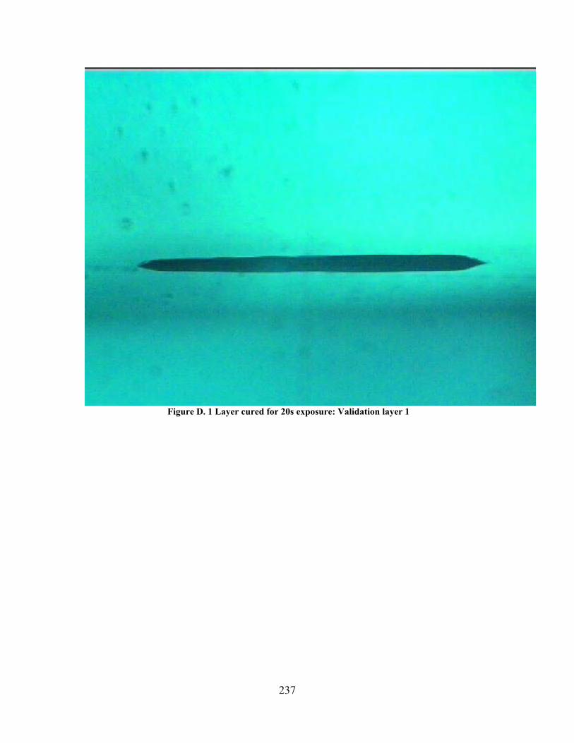
237
Figure D. 1 Layer cured for 20s exposure: Validation layer 1

238
Figure D. 2 Layer cured for 20s exposure: Validation layer 2

239
Figure D. 3 Layer cured for 20s exposure: Validation layer 3

240
Figure D. 4 Layer cured for 25s exposure: Validation layer 1

241
Figure D. 5 Layer cured for 25s exposure: Validation layer 2

242
Figure D. 6 Layer cured for 25s exposure: Validation layer 3
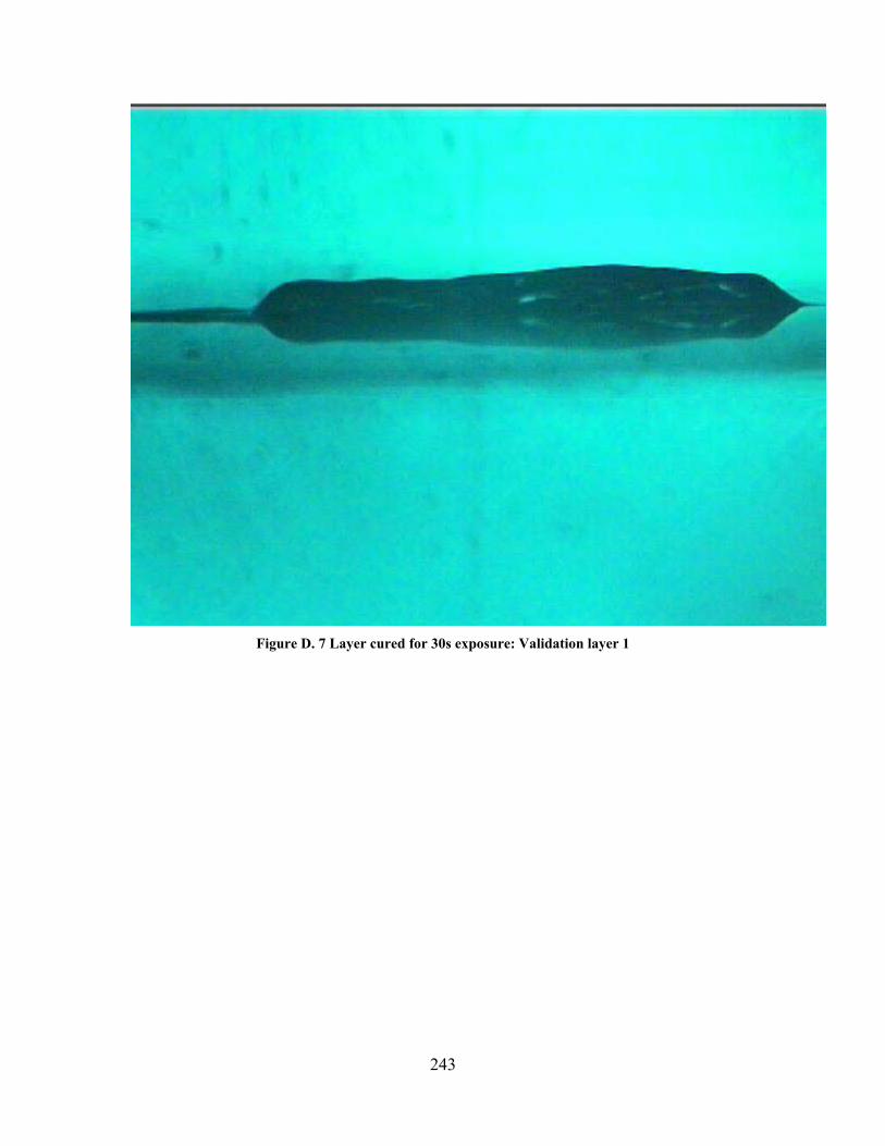
243
Figure D. 7 Layer cured for 30s exposure: Validation layer 1

244
Figure D. 8 Layer cured for 30s exposure: Validation layer 2
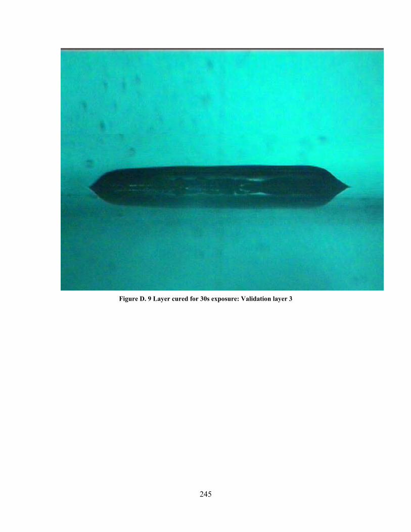
245
Figure D. 9 Layer cured for 30s exposure: Validation layer 3

246
Figure D. 10 Layer cured for 35s exposure: Validation layer 1

247
Figure D. 11 Layer cured for 35s exposure: Validation layer 2
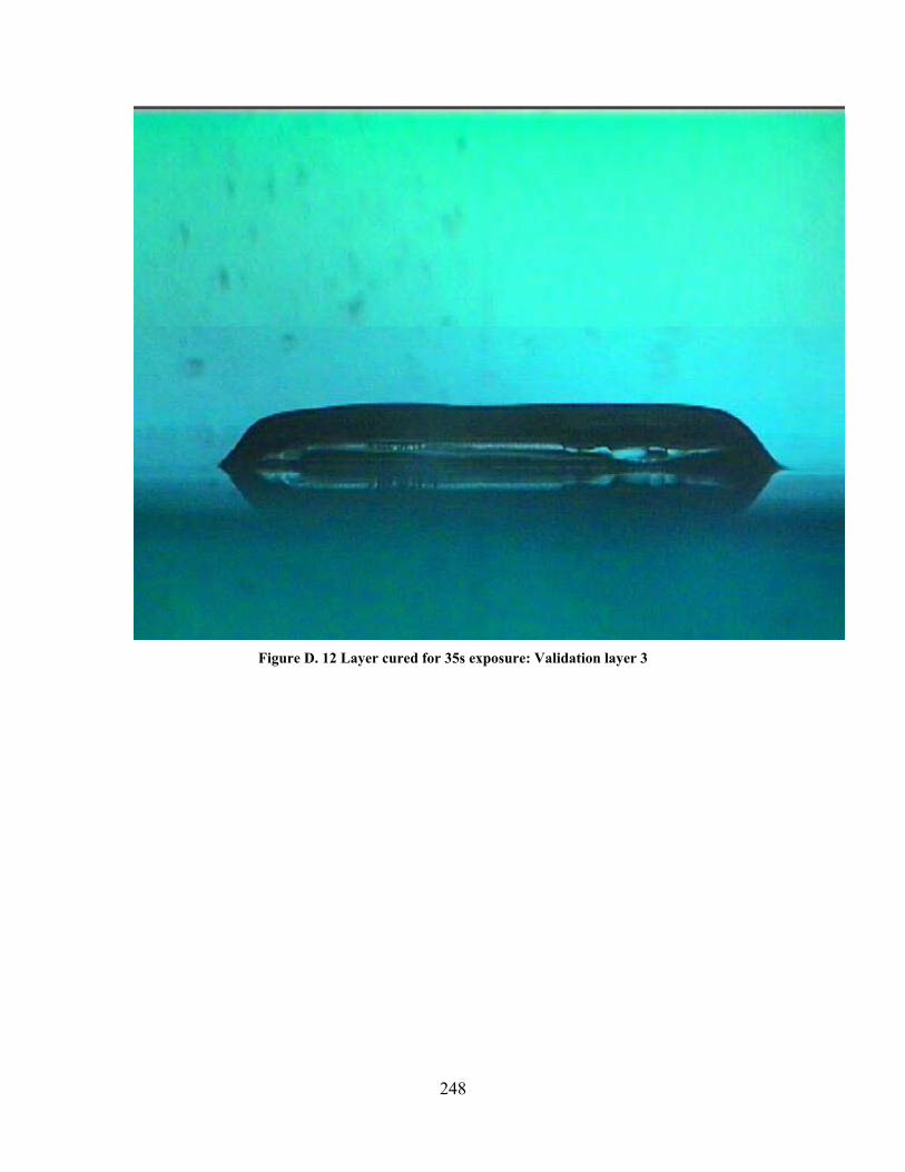
248
Figure D. 12 Layer cured for 35s exposure: Validation layer 3

249
Figure D. 13 Layer cured for 40s exposure: Validation layer 1
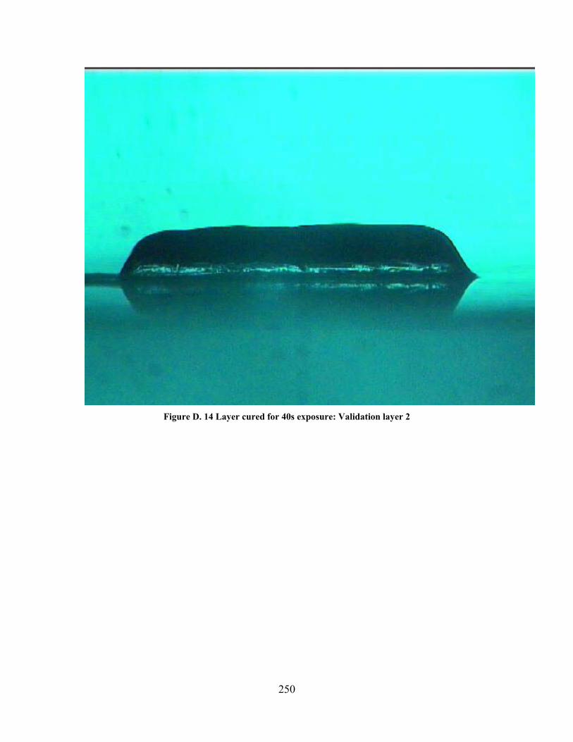
250
Figure D. 14 Layer cured for 40s exposure: Validation layer 2

251
Figure D. 15 Layer cured for 40s exposure: Validation layer 3
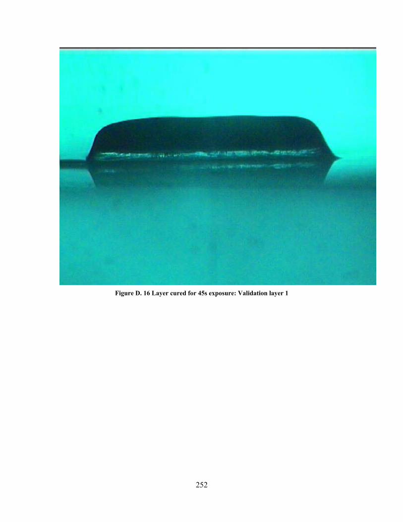
252
Figure D. 16 Layer cured for 45s exposure: Validation layer 1
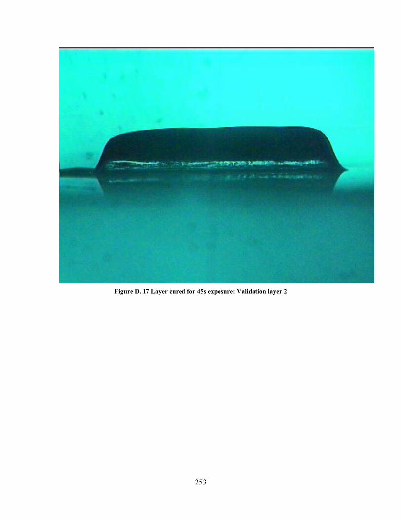
253
Figure D. 17 Layer cured for 45s exposure: Validation layer 2

254
Figure D. 18 Layer cured for 45s exposure: Validation layer 3
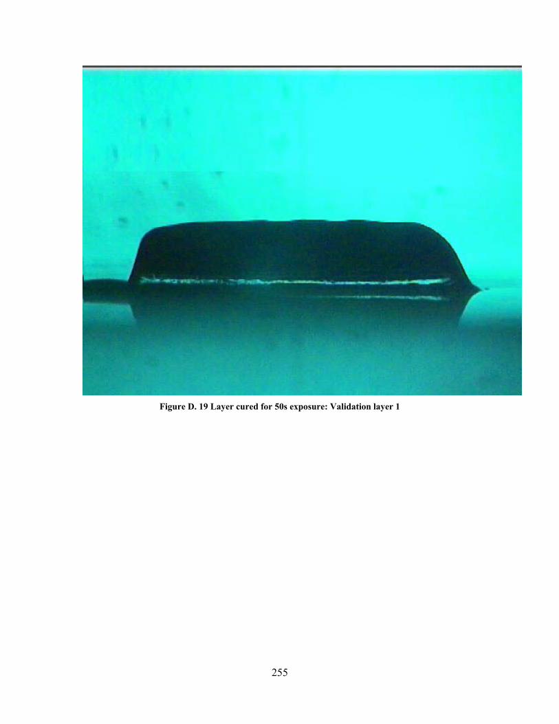
255
Figure D. 19 Layer cured for 50s exposure: Validation layer 1
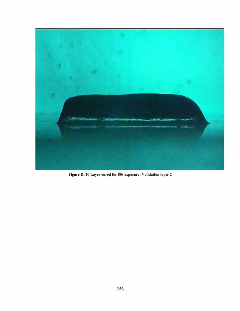
256
Figure D. 20 Layer cured for 50s exposure: Validation layer 2

257
Figure D. 21 Layer cured for 50s exposure: Validation layer 3
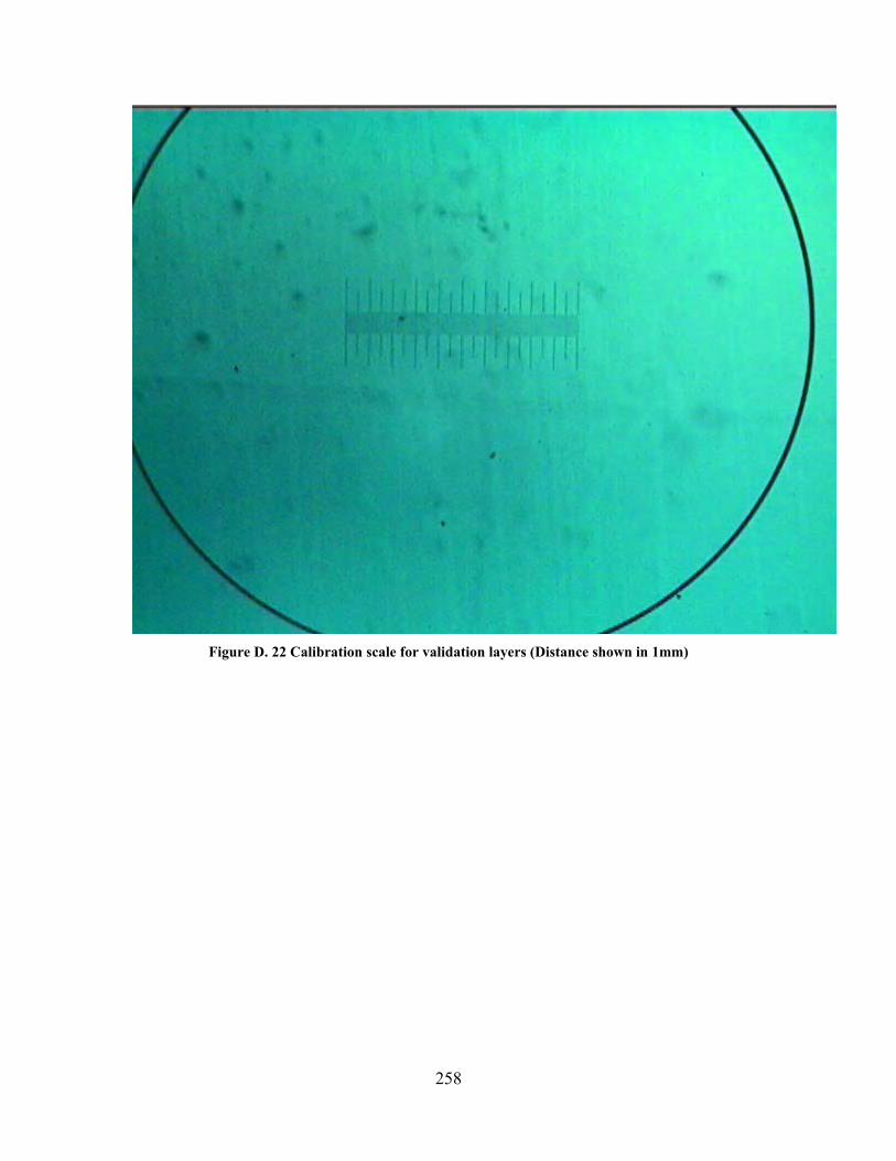
258
Figure D. 22 Calibration scale for validation layers (Distance shown in 1mm)

259
APPENDIX E. QUANTIFYING EFFECT OF RADICAL DIFFUSION
In this appendix, the pictures of the layers cured by supplying two discrete
exposure doses of 25s each are presented. The variable is the time interval (called waiting
time) allowed in between these two exposure doses. Greater the “waiting time”, greater is
the loss of energy from the bottom surface and smaller is the thickness of the layer cured
after the second exposure dose.
Experiments are conducted for 5 waiting times, of 4s, 30s, 60s, 120s, and 180s.
Three repeat experiments are conducted for each of these waiting times.
Figure E.1 Waiting time between exposures = 4s. Test layer 1

260
Figure E.2 Waiting time between exposures = 4s. Test layer 2
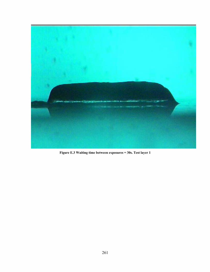
261
Figure E.3 Waiting time between exposures = 30s. Test layer 1
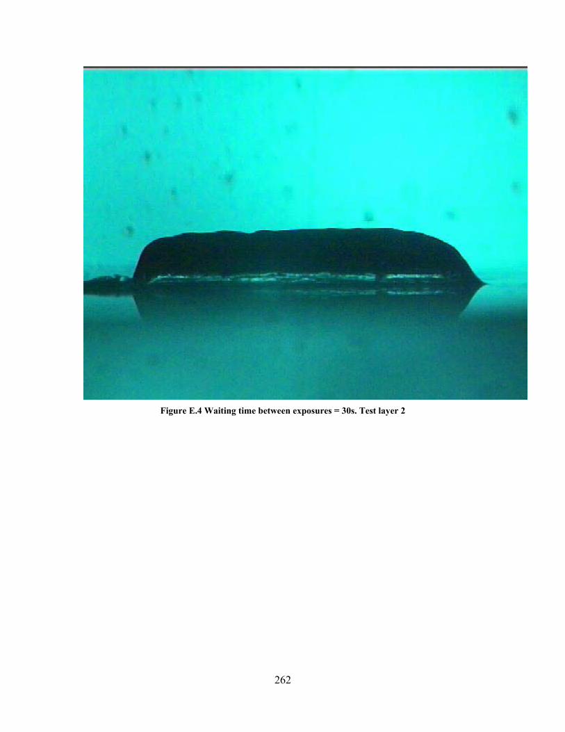
262
Figure E.4 Waiting time between exposures = 30s. Test layer 2
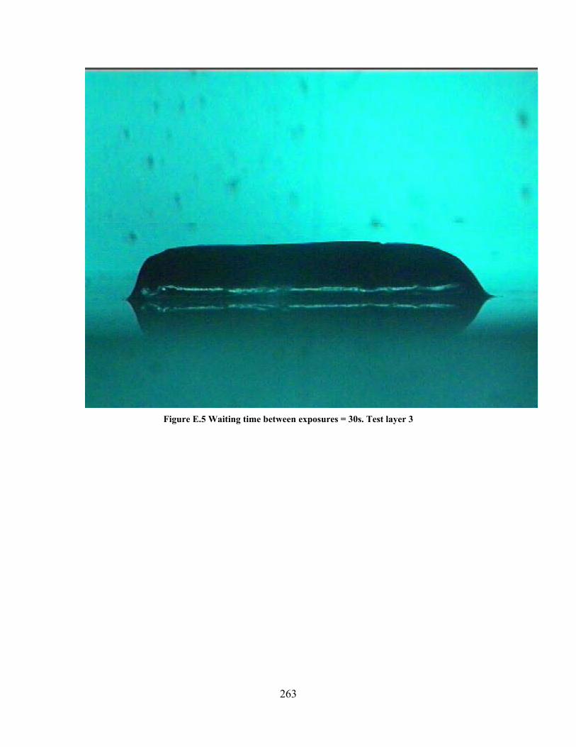
263
Figure E.5 Waiting time between exposures = 30s. Test layer 3

264
Figure E.6 Waiting time between exposures = 60s. Test layer 1
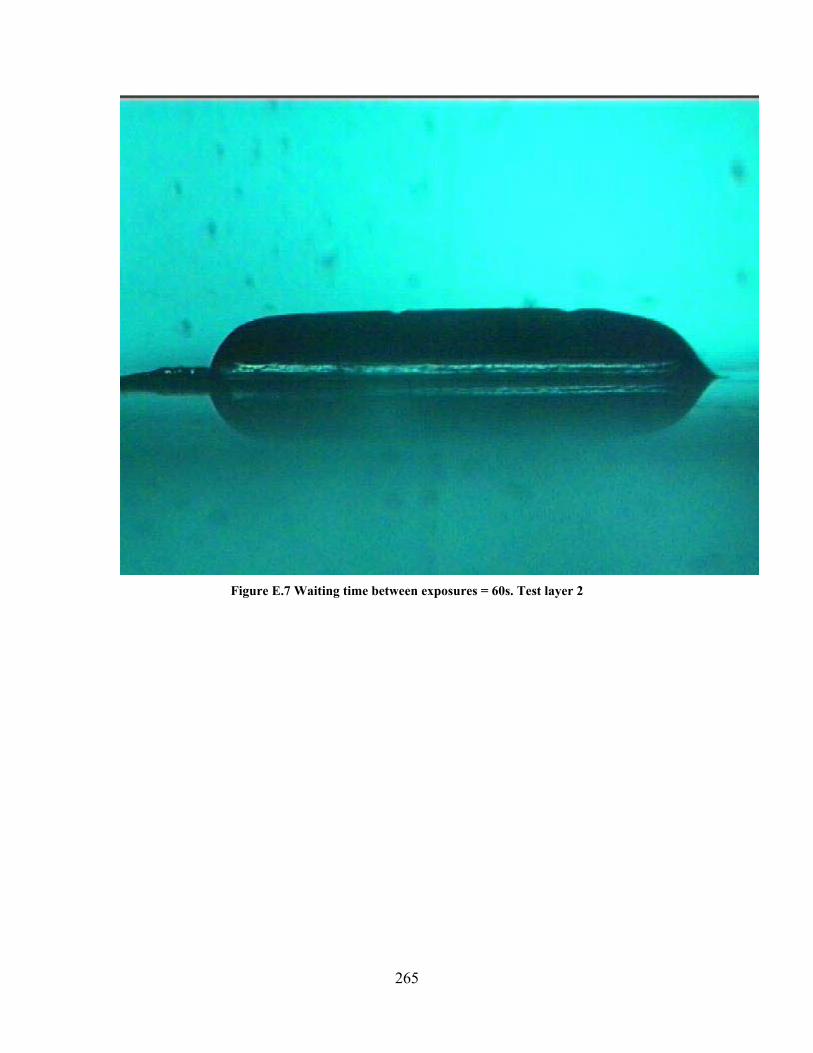
265
Figure E.7 Waiting time between exposures = 60s. Test layer 2

266
Figure E.8 Waiting time between exposures = 60s. Test layer 3
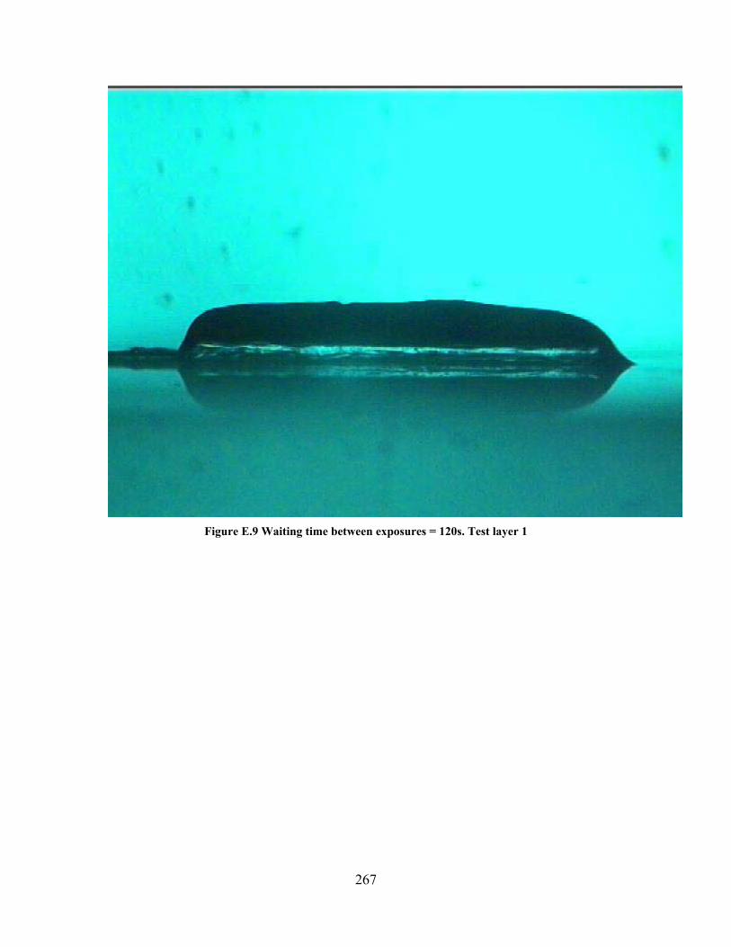
267
Figure E.9 Waiting time between exposures = 120s. Test layer 1
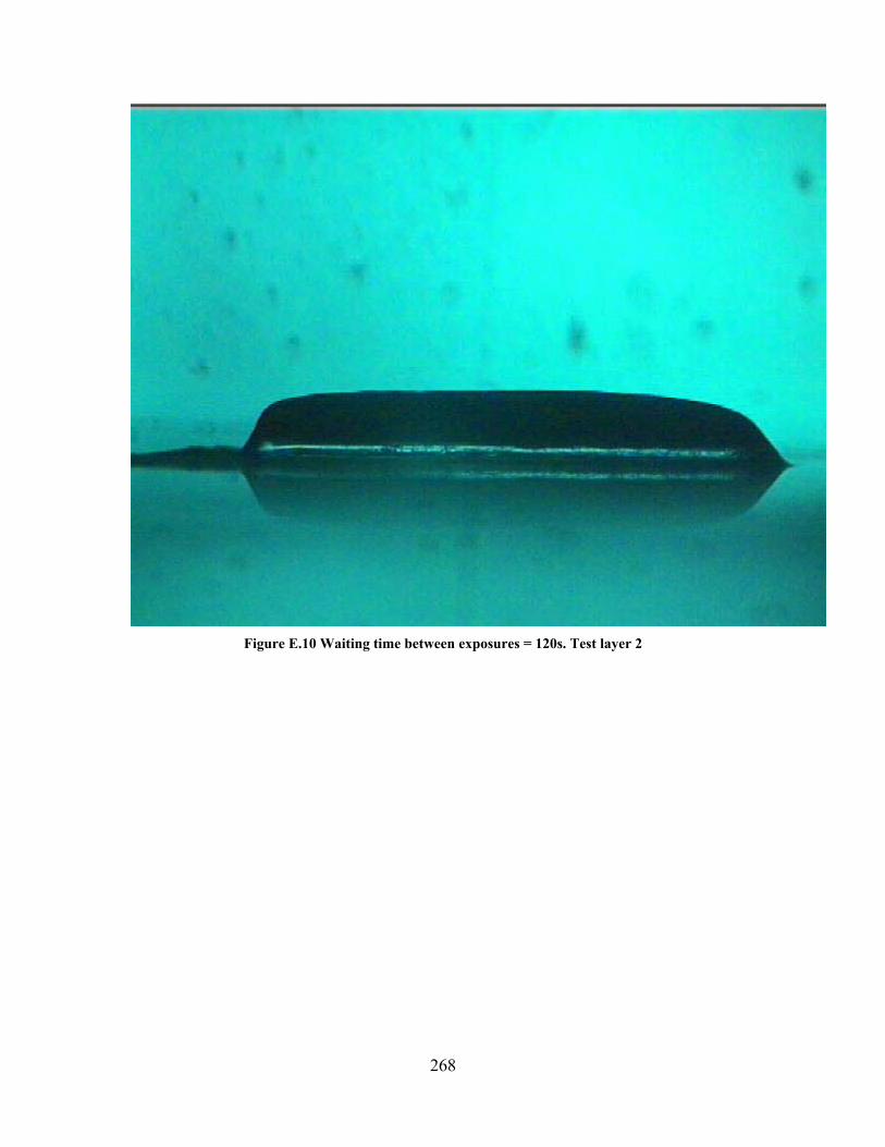
268
Figure E.10 Waiting time between exposures = 120s. Test layer 2
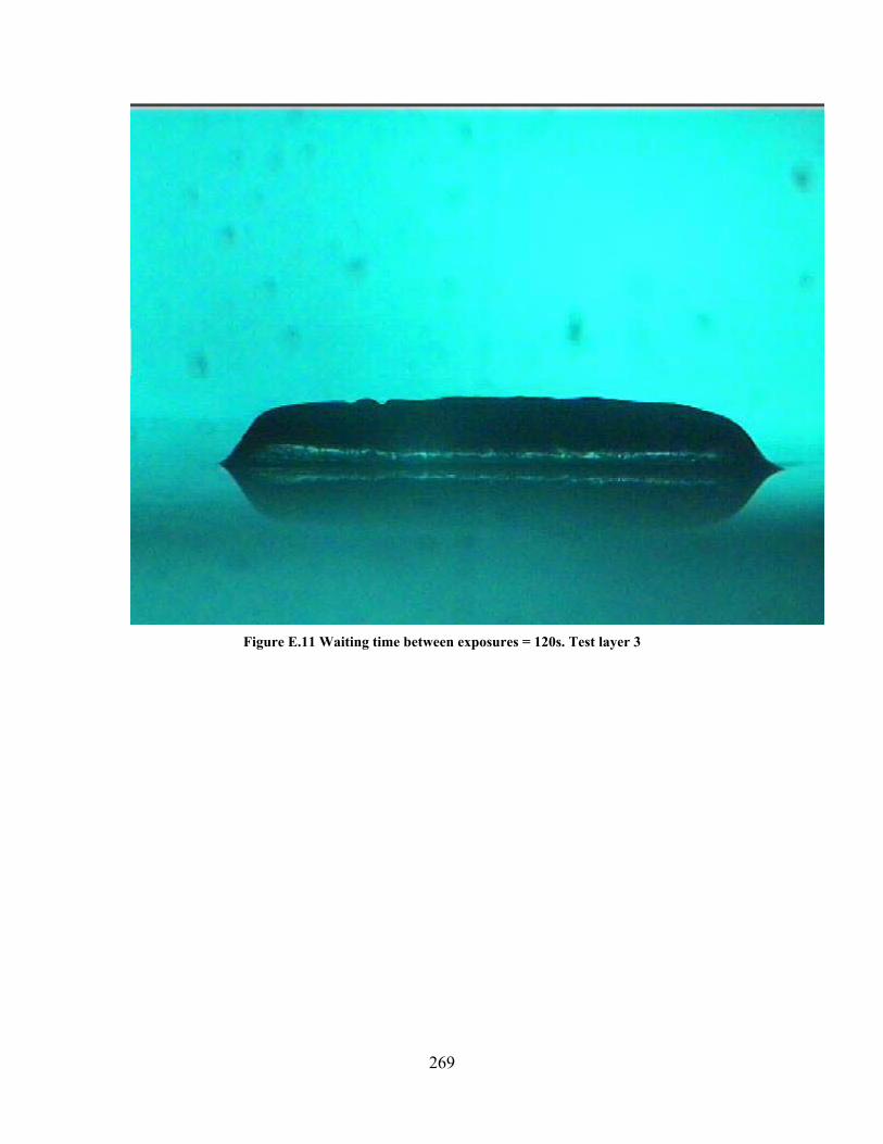
269
Figure E.11 Waiting time between exposures = 120s. Test layer 3
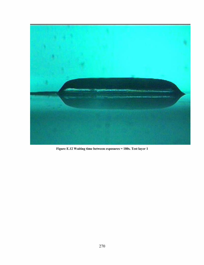
270
Figure E.12 Waiting time between exposures = 180s. Test layer 1
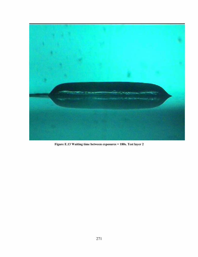
271
Figure E.13 Waiting time between exposures = 180s. Test layer 2

272
Figure E.14 Waiting time between exposures = 180s. Test layer 3
273
Figure E.15 Calibration scale for above layers (1 mm)
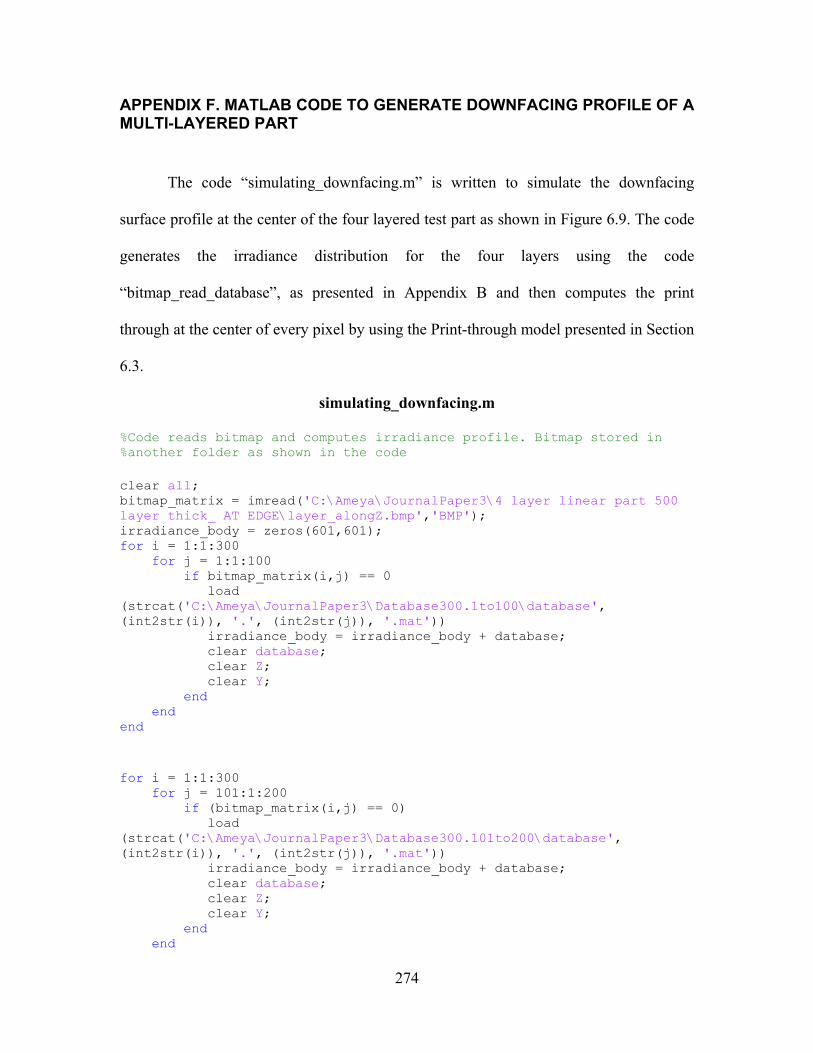
274
APPENDIX F. MATLAB CODE TO GENERATE DOWNFACING PROFILE OF A MULTI-LAYERED PART
The code “simulating_downfacing.m” is written to simulate the downfacing
surface profile at the center of the four layered test part as shown in Figure 6.9. The code
generates the irradiance distribution for the four layers using the code
“bitmap_read_database”, as presented in Appendix B and then computes the print
through at the center of every pixel by using the Print-through model presented in Section
6.3.
simulating_downfacing.m
%Code reads bitmap and computes irradiance profile. Bitmap stored in %another folder as shown in the code clear all; bitmap_matrix = imread('C:\Ameya\JournalPaper3\4 layer linear part 500 layer thick_ AT EDGE\layer_alongZ.bmp','BMP'); irradiance_body = zeros(601,601); for i = 1:1:300 for j = 1:1:100 if bitmap_matrix(i,j) == 0 load (strcat('C:\Ameya\JournalPaper3\Database300.1to100\database', (int2str(i)), '.', (int2str(j)), '.mat')) irradiance_body = irradiance_body + database; clear database; clear Z; clear Y; end end end for i = 1:1:300 for j = 101:1:200 if (bitmap_matrix(i,j) == 0) load (strcat('C:\Ameya\JournalPaper3\Database300.101to200\database', (int2str(i)), '.', (int2str(j)), '.mat')) irradiance_body = irradiance_body + database; clear database; clear Z; clear Y; end end
275
end for i = 1:1:300 for j = 201:1:300 if bitmap_matrix(i,j) == 0 load (strcat('C:\Ameya\JournalPaper3\Database300.201to300\database', (int2str(i)), '.', (int2str(j)), '.mat')) irradiance_body = irradiance_body + database; clear database; clear Z; clear Y; end end end for i = 1:1:601; for j = 1:1:601; for k = 1:1:2; B(i,j,k) = irradiance_body(i,j); end end end A = smooth3(smooth3(B)); irradiance = A(:,:,1); for i = 1:1:567; X(i) = 10*i; end factor = 0.7/max(max(irradiance)); irradiance = irradiance*factor; plot(X,max(irradiance)); %********************************************** %Code written to compute the cure depth taking into account that there is %different attenuation through a cured layer and through uncured resin %This code takes in the irradiance distribution on a resin surface. Then, %given a time of exposure, it computes the cure depth at all the points on %the resin surface. The time domain is discretized into deltat seconds. %DpL is the depth of penetration throug liquid and DpS through solid. %Code written by Ameya on June 27, 2007 clear irradiance1; clear irradiance2; clear irradiance3; clear irradiance4;
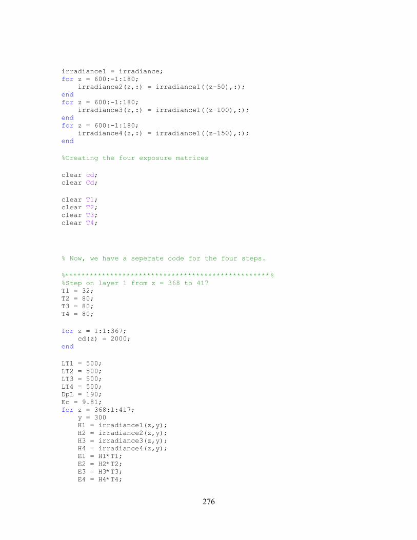
276
irradiance1 = irradiance; for z = 600:-1:180; irradiance2(z,:) = irradiance1((z-50),:); end for z = 600:-1:180; irradiance3(z,:) = irradiance1((z-100),:); end for z = 600:-1:180; irradiance4(z,:) = irradiance1((z-150),:); end %Creating the four exposure matrices clear cd; clear Cd; clear T1; clear T2; clear T3; clear T4; % Now, we have a seperate code for the four steps. %**************************************************% %Step on layer 1 from z = 368 to 417 T1 = 32; T2 = 80; T3 = 80; T4 = 80; for z = 1:1:367; cd(z) = 2000; end LT1 = 500; LT2 = 500; LT3 = 500; LT4 = 500; DpL = 190; Ec = 9.81; for z = 368:1:417; y = 300 H1 = irradiance1(z,y); H2 = irradiance2(z,y); H3 = irradiance3(z,y); H4 = irradiance4(z,y); E1 = H1*T1; E2 = H2*T2; E3 = H3*T3; E4 = H4*T4;

277
PT1 = 19.649*E1-207.72-LT1; EPT2 = E2 - (LT2+207.72)/19.649; %Energy seeping from 2nd layer waitingtime2 = 60 + (LT2+207.72)/19.649/H2; % Total waiting time k2 = 0.2629*log(waitingtime2)-0.3637; %Radical diffusion factor Eb = (1-k2)*Ec; %Energy already at bottom surfacel Eb2 = Eb + EPT2; %Total energy causing print through; PT2 = 19.649*Eb2-207.72; if PT2 < 0 PT2 = 0; end EPT3 = E3 - (LT3+207.72)/19.649; %Energy seeping from 3rd layer waitingtime3 = 60 + (LT3+207.72)/19.649/H3; % Total waiting time k3 = 0.2629*log(waitingtime3)-0.3637; %Radical diffusion factor Eb = (1-k3)*Ec; %Energy already at bottom surfacel Eb3 = Eb + EPT3; %Total energy causing print through; PT3 = 19.649*Eb3-207.72; if PT3 < 0 PT3 = 0; end EPT4 = E4 - (LT4+207.72)/19.649; %Energy seeping from 4th layer waitingtime4 = 60 + (LT4+207.72)/19.649/H4; % Total waiting time k4 = 0.2629*log(waitingtime4)-0.3637; %Radical diffusion factor Eb = (1-k4)*Ec; %Energy already at bottom surfacel Eb4 = Eb + EPT4; %Total energy causing print through; PT4 = 19.649*Eb4-207.72; if PT4 < 0 PT4 = 0; end cd(z) = LT1 + LT2 + LT3 + LT4 + PT1 + PT2 + PT3 + PT4; end %Step on layer 1 finished**********************************************************% %**************************************************% %Step on layer 2 from z = 418 to 467 clear T1; clear T2; clear T3; clear T4; T2 = 60; T3 = 80; T4 = 80; LT2 = 500;

278
LT3 = 500; LT4 = 500; DpL = 190; Ec = 9.81; for z = 418:1:467; y = 300; H2 = irradiance2(z,y); H3 = irradiance3(z,y); H4 = irradiance4(z,y); E2 = H2*T2; E3 = H3*T3; E4 = H4*T4; PT2 = 19.649*E2-207.72-LT2; EPT3 = E3 - (LT3+207.72)/19.649; %Energy seeping from 3rd layer waitingtime3 = 60 + (LT3+207.72)/19.649/H3; % Total waiting time k3 = 0.2629*log(waitingtime3)-0.3637; %Radical diffusion factor Eb = (1-k3)*Ec; %Energy already at bottom surfacel Eb3 = Eb + EPT3; %Total energy causing print through; PT3 = 19.649*Eb3-207.72; if PT3 < 0 PT3 = 0; end EPT4 = E4 - (LT4+207.72)/19.649; %Energy seeping from 4th layer waitingtime4 = 60 + (LT4+207.72)/19.649/H4; % Total waiting time k4 = 0.2629*log(waitingtime4)-0.3637; %Radical diffusion factor Eb = (1-k4)*Ec; %Energy already at bottom surfacel Eb4 = Eb + EPT4; %Total energy causing print through; PT4 = 19.649*Eb4-207.72; if PT4 < 0 PT4 = 0; end cd(z) = LT2 + LT3 + LT4 + PT2 + PT3 + PT4; end %Step on layer 2 finished**********************************************************% %**************************************************% %Step on layer 3 from z = 468 to 517 clear T1; clear T2; clear T3; clear T4; T3 = 65; T4 = 80; LT3 = 500; LT4 = 500; DpL = 190;
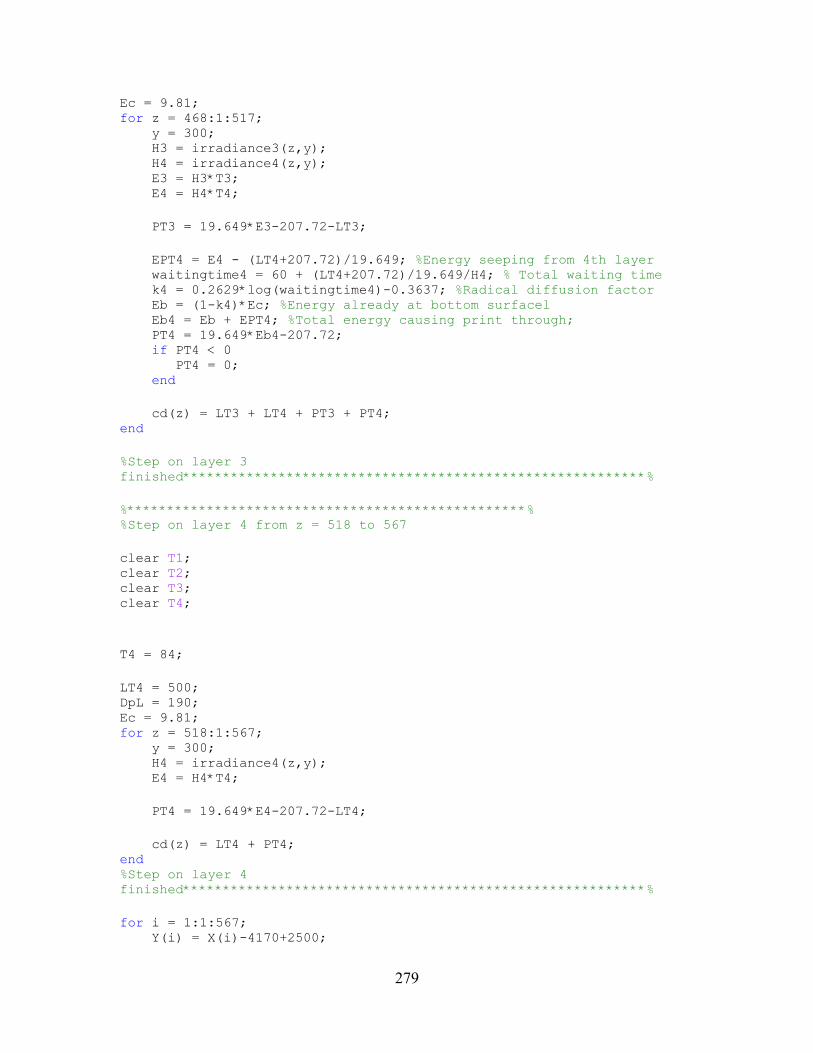
279
Ec = 9.81; for z = 468:1:517; y = 300; H3 = irradiance3(z,y); H4 = irradiance4(z,y); E3 = H3*T3; E4 = H4*T4; PT3 = 19.649*E3-207.72-LT3; EPT4 = E4 - (LT4+207.72)/19.649; %Energy seeping from 4th layer waitingtime4 = 60 + (LT4+207.72)/19.649/H4; % Total waiting time k4 = 0.2629*log(waitingtime4)-0.3637; %Radical diffusion factor Eb = (1-k4)*Ec; %Energy already at bottom surfacel Eb4 = Eb + EPT4; %Total energy causing print through; PT4 = 19.649*Eb4-207.72; if PT4 < 0 PT4 = 0; end cd(z) = LT3 + LT4 + PT3 + PT4; end %Step on layer 3 finished**********************************************************% %**************************************************% %Step on layer 4 from z = 518 to 567 clear T1; clear T2; clear T3; clear T4; T4 = 84; LT4 = 500; DpL = 190; Ec = 9.81; for z = 518:1:567; y = 300; H4 = irradiance4(z,y); E4 = H4*T4; PT4 = 19.649*E4-207.72-LT4; cd(z) = LT4 + PT4; end %Step on layer 4 finished**********************************************************% for i = 1:1:567; Y(i) = X(i)-4170+2500;

280
end Cd = 2000-cd plot(Y,Cd); axis equal line(1500:4000,2000) line(1500:4000,1500) line(4000,1500:2000) line(1500,1500:2000) line(1000:3500,1500) line(1000:3500,1000) line(3500,1000:1500) line(1000,1000:1500) line(500:3000,1000) line(500:3000,500) line(3000,500:1000) line(500,500:1000) line(0:2500,500) line(0:2500,0) line(2500,0:500) line(0,0:500)
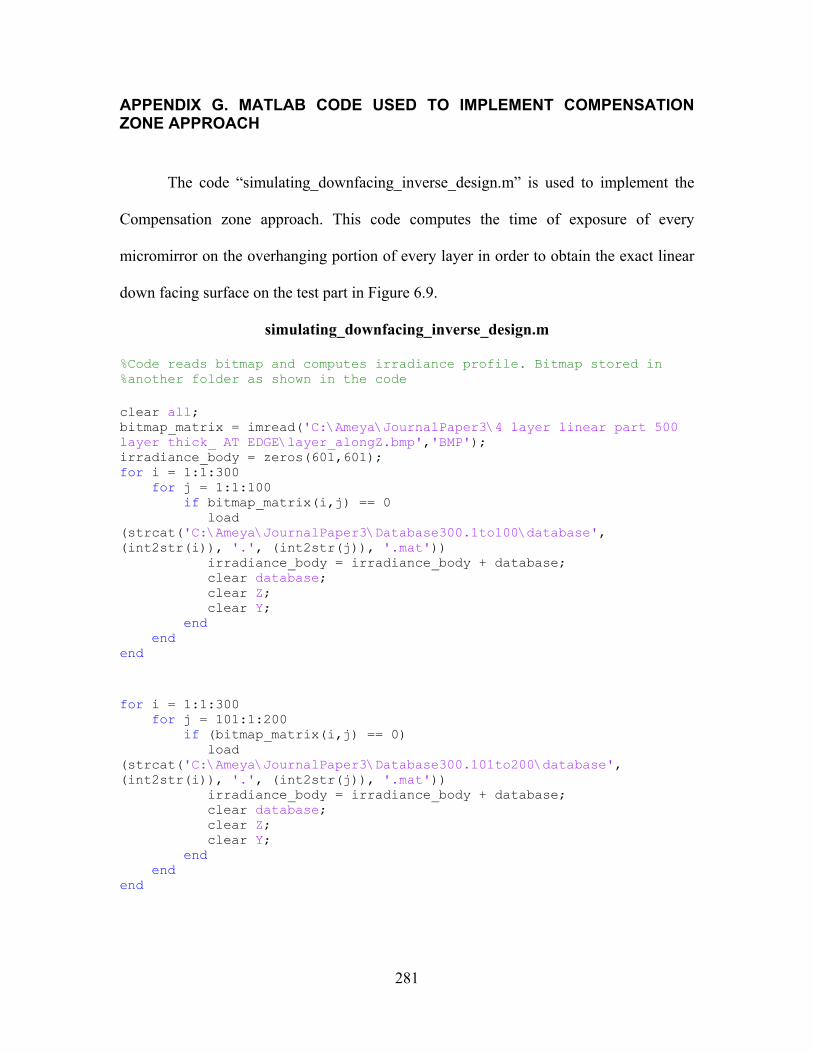
281
APPENDIX G. MATLAB CODE USED TO IMPLEMENT COMPENSATION ZONE APPROACH
The code “simulating_downfacing_inverse_design.m” is used to implement the
Compensation zone approach. This code computes the time of exposure of every
micromirror on the overhanging portion of every layer in order to obtain the exact linear
down facing surface on the test part in Figure 6.9.
simulating_downfacing_inverse_design.m
%Code reads bitmap and computes irradiance profile. Bitmap stored in %another folder as shown in the code clear all; bitmap_matrix = imread('C:\Ameya\JournalPaper3\4 layer linear part 500 layer thick_ AT EDGE\layer_alongZ.bmp','BMP'); irradiance_body = zeros(601,601); for i = 1:1:300 for j = 1:1:100 if bitmap_matrix(i,j) == 0 load (strcat('C:\Ameya\JournalPaper3\Database300.1to100\database', (int2str(i)), '.', (int2str(j)), '.mat')) irradiance_body = irradiance_body + database; clear database; clear Z; clear Y; end end end for i = 1:1:300 for j = 101:1:200 if (bitmap_matrix(i,j) == 0) load (strcat('C:\Ameya\JournalPaper3\Database300.101to200\database', (int2str(i)), '.', (int2str(j)), '.mat')) irradiance_body = irradiance_body + database; clear database; clear Z; clear Y; end end end
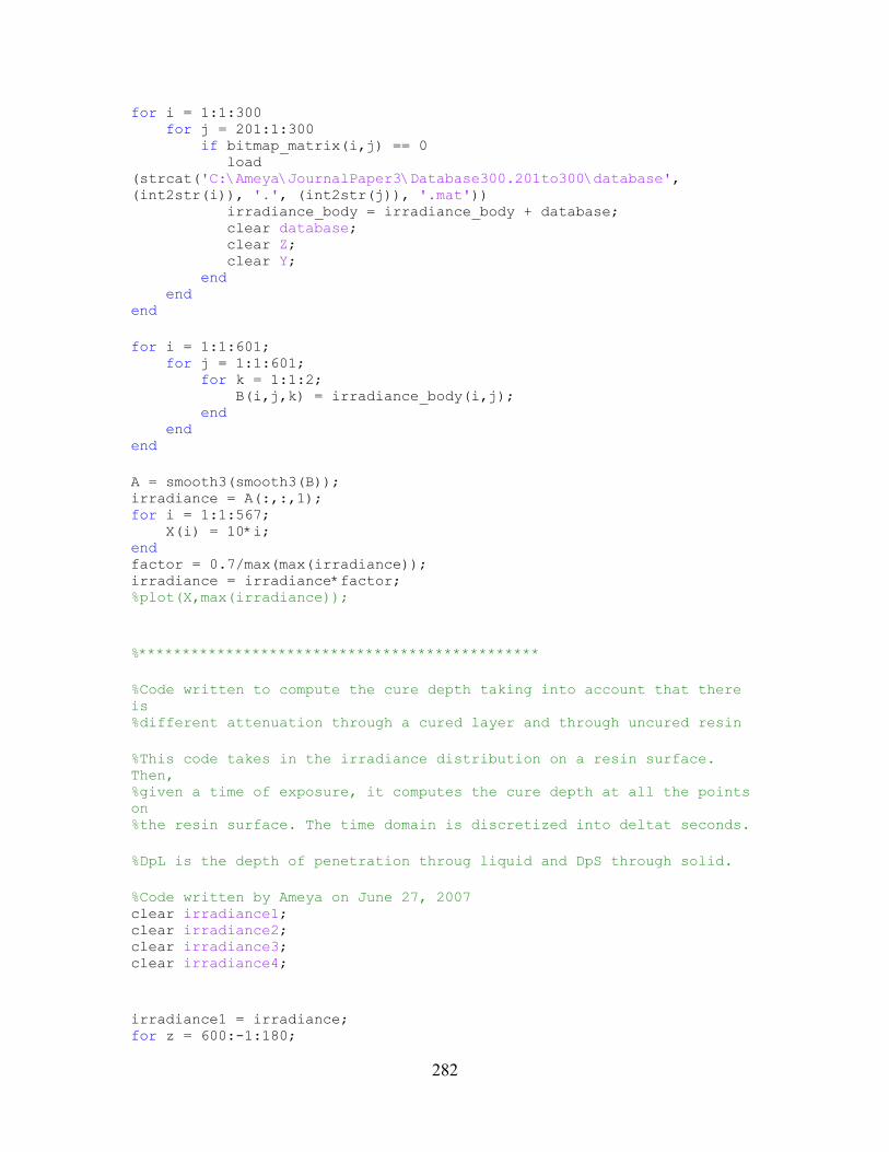
282
for i = 1:1:300 for j = 201:1:300 if bitmap_matrix(i,j) == 0 load (strcat('C:\Ameya\JournalPaper3\Database300.201to300\database', (int2str(i)), '.', (int2str(j)), '.mat')) irradiance_body = irradiance_body + database; clear database; clear Z; clear Y; end end end for i = 1:1:601; for j = 1:1:601; for k = 1:1:2; B(i,j,k) = irradiance_body(i,j); end end end A = smooth3(smooth3(B)); irradiance = A(:,:,1); for i = 1:1:567; X(i) = 10*i; end factor = 0.7/max(max(irradiance)); irradiance = irradiance*factor; %plot(X,max(irradiance)); %********************************************** %Code written to compute the cure depth taking into account that there is %different attenuation through a cured layer and through uncured resin %This code takes in the irradiance distribution on a resin surface. Then, %given a time of exposure, it computes the cure depth at all the points on %the resin surface. The time domain is discretized into deltat seconds. %DpL is the depth of penetration throug liquid and DpS through solid. %Code written by Ameya on June 27, 2007 clear irradiance1; clear irradiance2; clear irradiance3; clear irradiance4; irradiance1 = irradiance; for z = 600:-1:180;
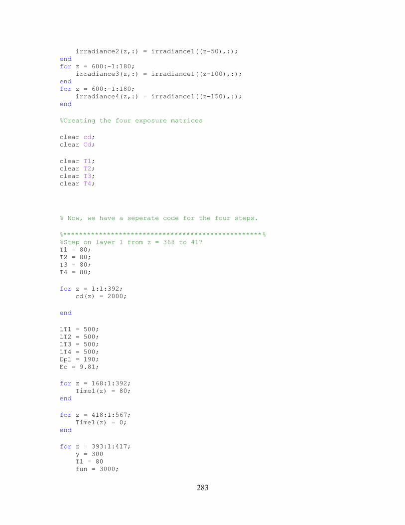
283
irradiance2(z,:) = irradiance1((z-50),:); end for z = 600:-1:180; irradiance3(z,:) = irradiance1((z-100),:); end for z = 600:-1:180; irradiance4(z,:) = irradiance1((z-150),:); end %Creating the four exposure matrices clear cd; clear Cd; clear T1; clear T2; clear T3; clear T4; % Now, we have a seperate code for the four steps. %**************************************************% %Step on layer 1 from z = 368 to 417 T1 = 80; T2 = 80; T3 = 80; T4 = 80; for z = 1:1:392; cd(z) = 2000; end LT1 = 500; LT2 = 500; LT3 = 500; LT4 = 500; DpL = 190; Ec = 9.81; for z = 168:1:392; Time1(z) = 80; end for z = 418:1:567; Time1(z) = 0; end for z = 393:1:417; y = 300 T1 = 80 fun = 3000;
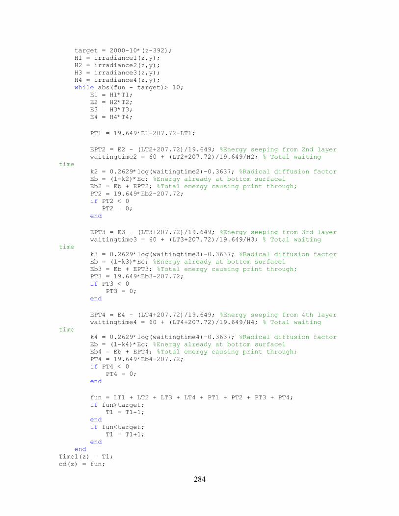
284
target = 2000-10*(z-392); H1 = irradiance1(z,y); H2 = irradiance2(z,y); H3 = irradiance3(z,y); H4 = irradiance4(z,y); while abs(fun - target)> 10; E1 = H1*T1; E2 = H2*T2; E3 = H3*T3; E4 = H4*T4; PT1 = 19.649*E1-207.72-LT1; EPT2 = E2 - (LT2+207.72)/19.649; %Energy seeping from 2nd layer waitingtime2 = 60 + (LT2+207.72)/19.649/H2; % Total waiting time k2 = 0.2629*log(waitingtime2)-0.3637; %Radical diffusion factor Eb = (1-k2)*Ec; %Energy already at bottom surfacel Eb2 = Eb + EPT2; %Total energy causing print through; PT2 = 19.649*Eb2-207.72; if PT2 < 0 PT2 = 0; end EPT3 = E3 - (LT3+207.72)/19.649; %Energy seeping from 3rd layer waitingtime3 = 60 + (LT3+207.72)/19.649/H3; % Total waiting time k3 = 0.2629*log(waitingtime3)-0.3637; %Radical diffusion factor Eb = (1-k3)*Ec; %Energy already at bottom surfacel Eb3 = Eb + EPT3; %Total energy causing print through; PT3 = 19.649*Eb3-207.72; if PT3 < 0 PT3 = 0; end EPT4 = E4 - (LT4+207.72)/19.649; %Energy seeping from 4th layer waitingtime4 = 60 + (LT4+207.72)/19.649/H4; % Total waiting time k4 = 0.2629*log(waitingtime4)-0.3637; %Radical diffusion factor Eb = (1-k4)*Ec; %Energy already at bottom surfacel Eb4 = Eb + EPT4; %Total energy causing print through; PT4 = 19.649*Eb4-207.72; if PT4 < 0 PT4 = 0; end fun = LT1 + LT2 + LT3 + LT4 + PT1 + PT2 + PT3 + PT4; if fun>target; T1 = T1-1; end if fun<target; T1 = T1+1; end end Time1(z) = T1; cd(z) = fun;

285
end %Step on layer 1 finished**********************************************************% %**************************************************% %Step on layer 2 from z = 418 to 467 clear T1; clear T2; clear T3; clear T4; T2 = 80; T3 = 80; T4 = 80; LT2 = 500; LT3 = 500; LT4 = 500; DpL = 190; Ec = 9.81; for z = 218:1:417; Time2(z) = 80; end for z = 468:1:567; Time2(z) = 0; end for z = 418:1:467; y = 300; T2 = 80; fun = 3000; target = 2000-10*(z-392); H2 = irradiance2(z,y); H3 = irradiance3(z,y); H4 = irradiance4(z,y); while abs(fun-target)>10; E2 = H2*T2; E3 = H3*T3; E4 = H4*T4; PT2 = 19.649*E2-207.72-LT2; EPT3 = E3 - (LT3+207.72)/19.649; %Energy seeping from 3rd layer waitingtime3 = 60 + (LT3+207.72)/19.649/H3; % Total waiting time k3 = 0.2629*log(waitingtime3)-0.3637; %Radical diffusion factor Eb = (1-k3)*Ec; %Energy already at bottom surfacel
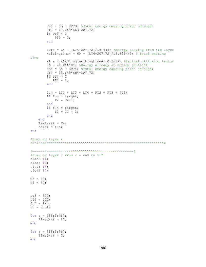
286
Eb3 = Eb + EPT3; %Total energy causing print through; PT3 = 19.649*Eb3-207.72; if PT3 < 0 PT3 = 0; end EPT4 = E4 - (LT4+207.72)/19.649; %Energy seeping from 4th layer waitingtime4 = 60 + (LT4+207.72)/19.649/H4; % Total waiting time k4 = 0.2629*log(waitingtime4)-0.3637; %Radical diffusion factor Eb = (1-k4)*Ec; %Energy already at bottom surfacel Eb4 = Eb + EPT4; %Total energy causing print through; PT4 = 19.649*Eb4-207.72; if PT4 < 0 PT4 = 0; end fun = LT2 + LT3 + LT4 + PT2 + PT3 + PT4; if fun > target; T2 = T2-1; end if fun < target; T2 = T2 + 1; end end Time2(z) = T2; cd(z) = fun; end %Step on layer 2 finished**********************************************************% %**************************************************% %Step on layer 3 from z = 468 to 517 clear T1; clear T2; clear T3; clear T4; T3 = 80; T4 = 80; LT3 = 500; LT4 = 500; DpL = 190; Ec = 9.81; for z = 268:1:467; Time3(z) = 80; end for z = 518:1:567; Time3(z) = 0; end

287
for z = 468:1:517; y = 300; T3 = 80; fun = 3000; target = 2000-10*(z-392); H3 = irradiance3(z,y); H4 = irradiance4(z,y); while abs(fun-target)>10; E3 = H3*T3; E4 = H4*T4; PT3 = 19.649*E3-207.72-LT3; EPT4 = E4 - (LT4+207.72)/19.649; %Energy seeping from 4th layer waitingtime4 = 60 + (LT4+207.72)/19.649/H4; % Total waiting time k4 = 0.2629*log(waitingtime4)-0.3637; %Radical diffusion factor Eb = (1-k4)*Ec; %Energy already at bottom surfacel Eb4 = Eb + EPT4; %Total energy causing print through; PT4 = 19.649*Eb4-207.72; if PT4 < 0 PT4 = 0; end fun = LT3 + LT4 + PT3 + PT4; if fun > target; T3 = T3 -1; end if fun < target; T3 = T3 + 1; end end Time3(z) = T3; cd(z) = fun; end %Step on layer 3 finished**********************************************************% %**************************************************% %Step on layer 4 from z = 518 to 567 clear T1; clear T2; clear T3; clear T4; T4 = 80; LT4 = 500;

288
DpL = 190; Ec = 9.81; for z = 317:1:517; Time4(z) = 80; end for z = 518:1:567; y = 300; fun = 3000; target = 2000-10*(z-392); while abs(fun-target) > 10; H4 = irradiance4(z,y); E4 = H4*T4; PT4 = 19.649*E4-207.72-LT4; fun = LT4 + PT4; if fun > target; T4 = T4 - 1; end if fun < target; T4 = T4 + 1; end end Time4(z) = T4; cd(z) = fun; end %Step on layer 4 finished**********************************************************% for i = 1:1:567; Y(i) = X(i)-4170+2500; end Cd = 2000-cd plot(Y,Cd); axis equal line(1500:4000,2000) line(1500:4000,1500) line(4000,1500:2000) line(1500,1500:2000) line(1000:3500,1500) line(1000:3500,1000) line(3500,1000:1500) line(1000,1000:1500) line(500:3000,1000) line(500:3000,500) line(3000,500:1000) line(500,500:1000) line(0:2500,500) line(0:2500,0) line(2500,0:500) line(0,0:500)

289
APPENDIX H. MATLAB CODE TO SIMULATE THE DOWN FACING SURFACE PROFILE OF A PART WITH THE OVERHANGING PORTION DISCRETIZED INTO TWO REGIONS
In the Matlab code “simulating_downfacing_discretized.m”, profile of the part
that would be cured for the times of exposure for every layer as mentioned in Section
6.5.2 is presented.
Simulating_downfacing_discretized.m
%Code reads bitmap and computes irradiance profile. Bitmap stored in %another folder as shown in the code clear all; bitmap_matrix = imread('C:\Ameya\JournalPaper3\4 layer linear part 500 layer thick_ AT EDGE\layer_alongZ.bmp','BMP'); irradiance_body = zeros(601,601); for i = 1:1:300 for j = 1:1:100 if bitmap_matrix(i,j) == 0 load (strcat('C:\Ameya\JournalPaper3\Database300.1to100\database', (int2str(i)), '.', (int2str(j)), '.mat')) irradiance_body = irradiance_body + database; clear database; clear Z; clear Y; end end end for i = 1:1:300 for j = 101:1:200 if (bitmap_matrix(i,j) == 0) load (strcat('C:\Ameya\JournalPaper3\Database300.101to200\database', (int2str(i)), '.', (int2str(j)), '.mat')) irradiance_body = irradiance_body + database; clear database; clear Z; clear Y; end end end for i = 1:1:300

290
for j = 201:1:300 if bitmap_matrix(i,j) == 0 load (strcat('C:\Ameya\JournalPaper3\Database300.201to300\database', (int2str(i)), '.', (int2str(j)), '.mat')) irradiance_body = irradiance_body + database; clear database; clear Z; clear Y; end end end for i = 1:1:601; for j = 1:1:601; for k = 1:1:2; B(i,j,k) = irradiance_body(i,j); end end end A = smooth3(smooth3(B)); irradiance = A(:,:,1); for i = 1:1:567; X(i) = 10*i; end factor = 0.7/max(max(irradiance)); irradiance = irradiance*factor; plot(X,max(irradiance)); %********************************************** %Code written to compute the cure depth taking into account that there is %different attenuation through a cured layer and through uncured resin %This code takes in the irradiance distribution on a resin surface. Then, %given a time of exposure, it computes the cure depth at all the points on %the resin surface. The time domain is discretized into deltat seconds. %DpL is the depth of penetration throug liquid and DpS through solid. %Code written by Ameya on June 27, 2007 clear irradiance1; clear irradiance2; clear irradiance3; clear irradiance4; irradiance1 = irradiance; for z = 600:-1:180; irradiance2(z,:) = irradiance1((z-50),:);

291
end for z = 600:-1:180; irradiance3(z,:) = irradiance1((z-100),:); end for z = 600:-1:180; irradiance4(z,:) = irradiance1((z-150),:); end %Creating the four exposure matrices clear cd; clear Cd; clear T1; clear T2; clear T3; clear T4; % Now, we have a seperate code for the four steps. %**************************************************% %Step on layer 1 from z = 368 to 417 T2 = 80; T3 = 80; T4 = 80; for z = 1:1:392; cd(z) = 2000; end LT1 = 500; LT2 = 500; LT3 = 500; LT4 = 500; DpL = 190; Ec = 9.81; for z = 393:1:417; T1 = 13.3 Time1(z) = T1; y = 300 H1 = irradiance1(z,y); H2 = irradiance2(z,y); H3 = irradiance3(z,y); H4 = irradiance4(z,y); E1 = H1*T1; E2 = H2*T2; E3 = H3*T3; E4 = H4*T4; PT1 = 19.649*E1-207.72-LT1;
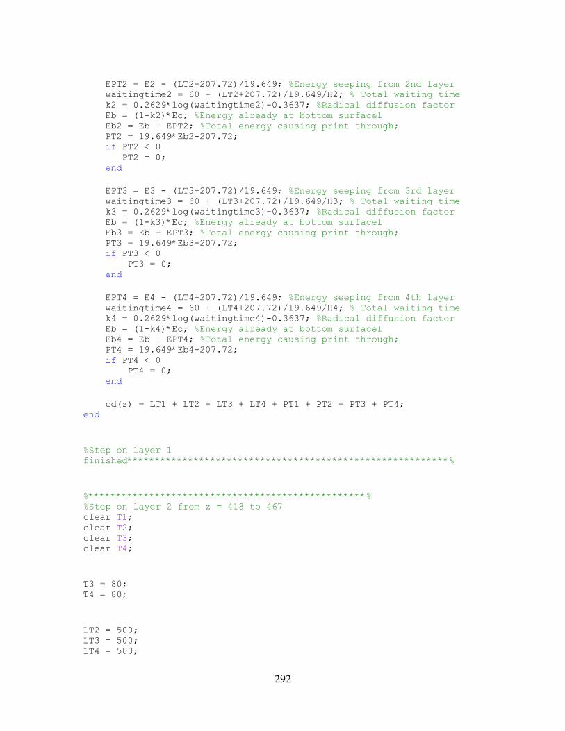
292
EPT2 = E2 - (LT2+207.72)/19.649; %Energy seeping from 2nd layer waitingtime2 = 60 + (LT2+207.72)/19.649/H2; % Total waiting time k2 = 0.2629*log(waitingtime2)-0.3637; %Radical diffusion factor Eb = (1-k2)*Ec; %Energy already at bottom surfacel Eb2 = Eb + EPT2; %Total energy causing print through; PT2 = 19.649*Eb2-207.72; if PT2 < 0 PT2 = 0; end EPT3 = E3 - (LT3+207.72)/19.649; %Energy seeping from 3rd layer waitingtime3 = 60 + (LT3+207.72)/19.649/H3; % Total waiting time k3 = 0.2629*log(waitingtime3)-0.3637; %Radical diffusion factor Eb = (1-k3)*Ec; %Energy already at bottom surfacel Eb3 = Eb + EPT3; %Total energy causing print through; PT3 = 19.649*Eb3-207.72; if PT3 < 0 PT3 = 0; end EPT4 = E4 - (LT4+207.72)/19.649; %Energy seeping from 4th layer waitingtime4 = 60 + (LT4+207.72)/19.649/H4; % Total waiting time k4 = 0.2629*log(waitingtime4)-0.3637; %Radical diffusion factor Eb = (1-k4)*Ec; %Energy already at bottom surfacel Eb4 = Eb + EPT4; %Total energy causing print through; PT4 = 19.649*Eb4-207.72; if PT4 < 0 PT4 = 0; end cd(z) = LT1 + LT2 + LT3 + LT4 + PT1 + PT2 + PT3 + PT4; end %Step on layer 1 finished**********************************************************% %**************************************************% %Step on layer 2 from z = 418 to 467 clear T1; clear T2; clear T3; clear T4; T3 = 80; T4 = 80; LT2 = 500; LT3 = 500; LT4 = 500;

293
DpL = 190; Ec = 9.81; for z = 418:1:442; T2 = 40.1; Time2(z) = T2; y = 300; H2 = irradiance2(z,y); H3 = irradiance3(z,y); H4 = irradiance4(z,y); E2 = H2*T2; E3 = H3*T3; E4 = H4*T4; PT2 = 19.649*E2-207.72-LT2; EPT3 = E3 - (LT3+207.72)/19.649; %Energy seeping from 3rd layer waitingtime3 = 60 + (LT3+207.72)/19.649/H3; % Total waiting time k3 = 0.2629*log(waitingtime3)-0.3637; %Radical diffusion factor Eb = (1-k3)*Ec; %Energy already at bottom surfacel Eb3 = Eb + EPT3; %Total energy causing print through; PT3 = 19.649*Eb3-207.72; if PT3 < 0 PT3 = 0; end EPT4 = E4 - (LT4+207.72)/19.649; %Energy seeping from 4th layer waitingtime4 = 60 + (LT4+207.72)/19.649/H4; % Total waiting time k4 = 0.2629*log(waitingtime4)-0.3637; %Radical diffusion factor Eb = (1-k4)*Ec; %Energy already at bottom surfacel Eb4 = Eb + EPT4; %Total energy causing print through; PT4 = 19.649*Eb4-207.72; if PT4 < 0 PT4 = 0; end cd(z) = LT2 + LT3 + LT4 + PT2 + PT3 + PT4; end for z = 443:1:467; T2 = 26.3; Time2(z) = T2; y = 300; H2 = irradiance2(z,y); H3 = irradiance3(z,y); H4 = irradiance4(z,y); E2 = H2*T2; E3 = H3*T3; E4 = H4*T4; PT2 = 19.649*E2-207.72-LT2; EPT3 = E3 - (LT3+207.72)/19.649; %Energy seeping from 3rd layer waitingtime3 = 60 + (LT3+207.72)/19.649/H3; % Total waiting time k3 = 0.2629*log(waitingtime3)-0.3637; %Radical diffusion factor Eb = (1-k3)*Ec; %Energy already at bottom surfacel
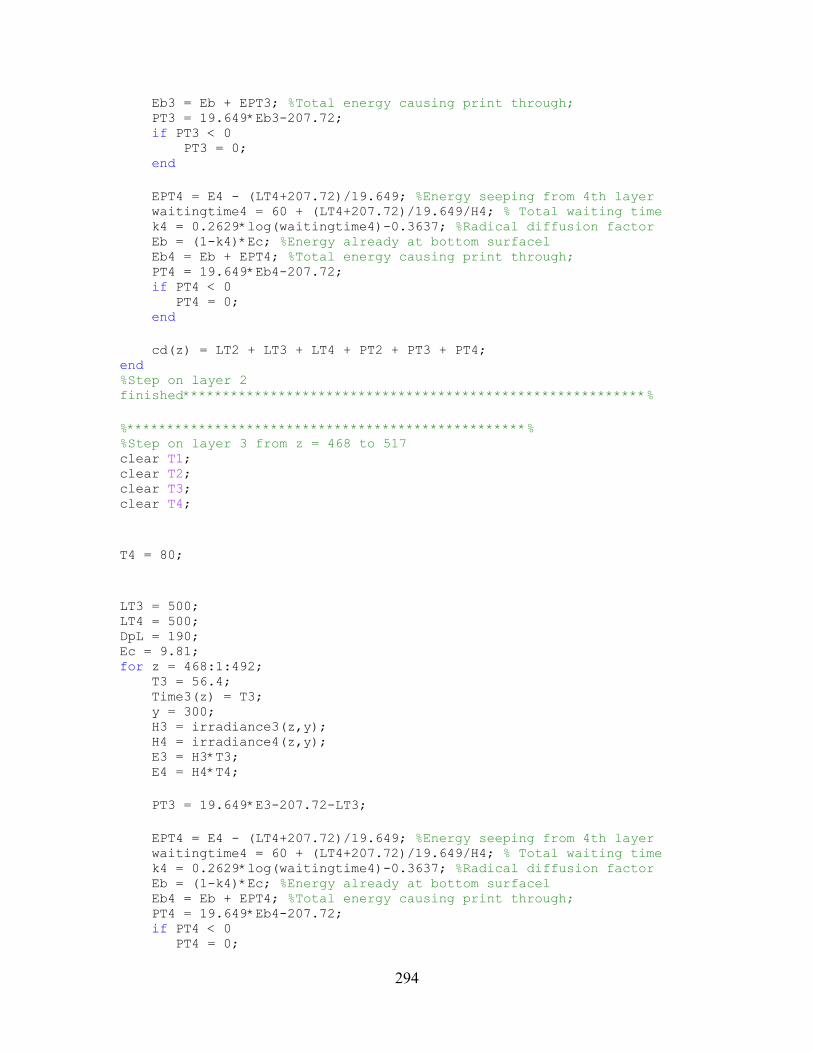
294
Eb3 = Eb + EPT3; %Total energy causing print through; PT3 = 19.649*Eb3-207.72; if PT3 < 0 PT3 = 0; end EPT4 = E4 - (LT4+207.72)/19.649; %Energy seeping from 4th layer waitingtime4 = 60 + (LT4+207.72)/19.649/H4; % Total waiting time k4 = 0.2629*log(waitingtime4)-0.3637; %Radical diffusion factor Eb = (1-k4)*Ec; %Energy already at bottom surfacel Eb4 = Eb + EPT4; %Total energy causing print through; PT4 = 19.649*Eb4-207.72; if PT4 < 0 PT4 = 0; end cd(z) = LT2 + LT3 + LT4 + PT2 + PT3 + PT4; end %Step on layer 2 finished**********************************************************% %**************************************************% %Step on layer 3 from z = 468 to 517 clear T1; clear T2; clear T3; clear T4; T4 = 80; LT3 = 500; LT4 = 500; DpL = 190; Ec = 9.81; for z = 468:1:492; T3 = 56.4; Time3(z) = T3; y = 300; H3 = irradiance3(z,y); H4 = irradiance4(z,y); E3 = H3*T3; E4 = H4*T4; PT3 = 19.649*E3-207.72-LT3; EPT4 = E4 - (LT4+207.72)/19.649; %Energy seeping from 4th layer waitingtime4 = 60 + (LT4+207.72)/19.649/H4; % Total waiting time k4 = 0.2629*log(waitingtime4)-0.3637; %Radical diffusion factor Eb = (1-k4)*Ec; %Energy already at bottom surfacel Eb4 = Eb + EPT4; %Total energy causing print through; PT4 = 19.649*Eb4-207.72; if PT4 < 0 PT4 = 0;

295
end cd(z) = LT3 + LT4 + PT3 + PT4; end for z = 493:1:517; T3 = 46.8; Time3(z) = T3; y = 300; H3 = irradiance3(z,y); H4 = irradiance4(z,y); E3 = H3*T3; E4 = H4*T4; PT3 = 19.649*E3-207.72-LT3; EPT4 = E4 - (LT4+207.72)/19.649; %Energy seeping from 4th layer waitingtime4 = 60 + (LT4+207.72)/19.649/H4; % Total waiting time k4 = 0.2629*log(waitingtime4)-0.3637; %Radical diffusion factor Eb = (1-k4)*Ec; %Energy already at bottom surfacel Eb4 = Eb + EPT4; %Total energy causing print through; PT4 = 19.649*Eb4-207.72; if PT4 < 0 PT4 = 0; end cd(z) = LT3 + LT4 + PT3 + PT4; end %Step on layer 3 finished**********************************************************% %**************************************************% %Step on layer 4 from z = 518 to 567 clear T1; clear T2; clear T3; clear T4; LT4 = 500; DpL = 190; Ec = 9.81; for z = 518:1:542; T4 = 71.8; Time4(z) = T4; y = 300; H4 = irradiance4(z,y); E4 = H4*T4; PT4 = 19.649*E4-207.72-LT4;

296
cd(z) = LT4 + PT4; end for z = 543:1:567; T4 = 57.4; Time4(z) = T4; y = 300; H4 = irradiance4(z,y); E4 = H4*T4; PT4 = 19.649*E4-207.72-LT4; cd(z) = LT4 + PT4; end %Step on layer 4 finished**********************************************************% for i = 1:1:567; Y(i) = X(i)-4170+2500; end Cd = 2000-cd plot(Y,Cd); axis equal line(1500:4000,2000) line(1500:4000,1500) line(4000,1500:2000) line(1500,1500:2000) line(1000:3500,1500) line(1000:3500,1000) line(3500,1000:1500) line(1000,1000:1500) line(500:3000,1000) line(500:3000,500) line(3000,500:1000) line(500,500:1000) line(0:2500,500) line(0:2500,0) line(2500,0:500) line(0,0:500)

297
APPENDIX I. MATLAB CODE TO IMPLEMENT ROSEN’S GRADIENT PROJECTION ALGORITHM TO OPTIMIZE THE DEVIATION FUNCTION OF THE SLICING COMPROMISE DSP
In the Matlab code “gradient_projection.m”, an exhaustive search across the
entire range of the possible number of layers, from 3 to 30 is performed. For every
number of layers, the gradient projection method is executed as explained in Chapter 7.
The Matlab code “f.m” computes the value of the deviation function. “f.m” is called as a
function from the code “gradient_pojection.m”.
gradient_projection.m
%Rosens gradient projectin method to solve the slicing optimization problem %Written on 15th September 2007 clear all; %Calculating the projection matrix for n = 3:1:30; for i = 1:1:n; B(i) = 1; end clear i; P = eye(n)- transpose(B)*(inv(B*transpose(B)))*B; %Calculating delf for i = 1:1:n; xstart(i) = 1800/n; end clear i; direction = [100,100]; clear count; count = 1; while (sum(abs(direction))>1e-5 & count < 100); direction1 = direction; clear direction; Z = f(xstart); for i = 1:1:n;

298
xstart1 = xstart; xstart1(i) = xstart(i) + 0.1; Z1 = f(xstart1); delf(i) = Z1-Z; clear xstart1; end clear i; delf = transpose(delf); d0 = P*delf; direction = d0; d0 = -d0; maxd0 = max(abs(d0)); if maxd0>0; d0 = d0/maxd0; alpha = 2; while alpha >=(1/4096) xstart1 = xstart + alpha*transpose(d0); if f(xstart1) < f(xstart) xstart = xstart1; else alpha = alpha/2; end end end clear delf; count = count + 1; end n xstart f(xstart) end
f.m
%Here, the function f is defined function Z = f(x) %Evaluating delta and d1plus for count1 = 2:1:max(size(x)); sum1 = 0; sum2 = 0; for i = 1:1:count1; sum1 = sum1 + x(i); end clear i; for i = 1:1:count1-1; sum2 = sum2 + x(i); end if sum1 <= 1200; r1 = ((1200-sum1)^2)/7200 + 400; end if sum1 >1200; r1 = -((sum1-1200)^2)/1200 + 400; end
299
if sum2 <= 1199; r2 = ((1200-sum2)^2)/7200 + 400; end if sum2 >1200; r2 = -((sum2-1200)^2)/1200 + 400; end deltar(count1) = abs(r1-r2); theta(count1) = atan(deltar(count1)/x(count1)); delta(count1) = x(count1)*sin(theta(count1)); end theta1 = atan(abs(((1200-x(1))^2/7200-200)/x(1))); delta1 = abs((x(1)*sin(theta1))); Max1Delta = max(delta); MaxDelta = max(Max1Delta, delta1); d1plus = (MaxDelta - 40)/40; if d1plus < 0; d1plus = 0; end clear count1; %Now, evaluating the build time BT = 0; for i = 1:1:max(size(x)) Ttrans = 10; Tsettle = 30000/x(i); Texp = ((x(i)+40)/19.172+10.5)/0.7; BT = BT + Ttrans + Tsettle + Texp; clear Ttrans; clear Tsettle; clear Texp; end d2plus = (BT-4200)/4200; if d2plus < 0; d2plus = 0; end %Evauating the penalty function penalty = 0; for i = 1:1:max(size(x)); if x(i) - 600 < 0; temp1 = 0; else temp1 = x(i) - 600; end if 60-x(i) < 0; temp2 = 0; else temp2 = 60-x(i); end penalty = penalty + temp1 + temp2; clear temp1; clear temp2; end Z = 0*d1plus + 1*d2plus + 1000000*penalty;
300
REFERENCES
Accumax Toolkit User Guide, 1996, 3D Systems Inc., Valencia CA. Bayt R. and Breuer K., 2000, “Fabrication and testing of micron sized cold-gas thrusters”, Progress in Astronautics and Aeronautics series, 147, pp.381. Belegundu A. D., Chadrupatla T. R., 1999, “Optimization Concepts and Applications in Engineering”, Prentice Hall Inc. Beluze L., Bertsch A., Renaud P., 1999, “Microstereolithography: a new process to build complex 3D objects”, SPIE Symposium on design, test and microfabrication of MEMS/MOEMS, Vol. 3680, pp. 808-17.
Bertsch A., Zissi S., Jezequel J., Corbel S., Andre J., 1997, “Microstereolithography using liquid crystal display as dynamic mask-generator”, Microsystems Technologies, pp.42-47.
Bertsch A., Jezequel J. Y., Andre J.C., 1997, “Study of spatial resolution of a new 3D microfabrication process: the microstereolithography using a dynamic mask-generator technique”, Journal of Photochemistrey ad Photobiology A: Chemistry 107, pp. 275-281.
Bertsch A., Bernhard P., Vogt C., Renaud P., 2000, “Rapid prototyping of small size objects”, Rapid Prototyping Journal, Vol. 6, Number 4, pp. 259-266. Bertsch A., Bernhard P., Renaud P., 2001, “Microstereolithography: Concepts and applications”, IEEE pp. 289-298. Bertsch A., Jiguet S., Renaud P., 2004, “Microfabrication of ceramic components by microstereolithography”, Journal of Micromechanics and Microengineering, pp.197-203 Chatwin C., Farsari M., Huang S., Heywood M., Birch P., Young R., Richardson J., 1998, “UV microstereolithography system that uses spatial light modulator technology”, Applied Optics, Vol. 37, pp.7514-22.
Chatwin C., Farsari M., Huang S., Heywood M., Young R., Bitch P., Claret-Tournier F., Richardson J., 1999, “Characterisation of epoxy resins for microstereolithographic rapid prototyping”, International Journal of Advanced Manufacturing technologies, Vol. 15, pp.281-6.
Chen C. and Sullivan P., 1996, “Predicting total build time and the resultant cure depth of the 3D stereolithography process”, Rapid Prototyping Journal, Vol. 2, Number 4, pp.27-40

301
Drobny J., 2002, “Radiation technology for polymers”, CRC press. Dudley D., Duncan W., Slaughter J., 2003, “Emerging Digital Micromirror Device (DMD) applications”, SPIE proceedings, Vol. 4985.
Edmund Industrial Optics 2003, “Optical and optical instruments Catalog”.
Farsari M., Huang S., Birch P., Claret-Tournier F., Young R., Budgett D., Bradfield C., Chatwin C., 1999, “Microfabrication by use of spatial light modulator in the ultraviolet: experimental results”, Optics Letters, Vol. 24, No. 8, pp. 549-50.
Farsari M., Claret-Tournier F., Huang S., Chatwin C., Budgett D., Birch P., Young R., Richardson J., 2000, “A novel high-accuracy microstereolithography method employing an adaptive electro-optic mask”, Journal of Material Processing Technology 107, pp. 167-172.
Fujimasa I., 1996, “Micromachines: A new era in Mechanical Engineering”, Oxford University Press.
Gardner J., Varadan V., Awadelkarim O., 2001, “Microsensors MEMS and Smart Devices”, John Wiley and Sons.
Hadipoespito G., Yang Y., Choi H., Ning G., Li X., 2003, “Digital Micromirror device based microstereolithography for micro structures of transparent photopolymer and nanocomposites”, Proceedings of the Solid Freeform Fabrication Symposium, Austin Texas, pp. 13-24.
Hope R., Roth R., Jacobs P., 1997, “Adaptive slicing with sloping layer surfaces”, Rapid Prototyping Journal, Vol. 3, Number 3, pp. 89-98
Ikuta K., Hirowatari K., 1993, “Real three dimensional micro fabrication using Stereolithography and metal molding”, Proceedings IEEE MEMS, pp.42-47.
Ikuta K., Maruo S., Yuichiro F., Fujisawa T., 1998, “Biomedical IC chip towards cell free DNA protein synthesis”, Proceedings of the IEEE International Workshop on Micro Electro Mechanical Systems (MEMS98), pp. 131-136 Ikuta K., Maruo S., Fujisawa T., Yamada A., 1999, “Micro concentrator with Opto-sense Micro Reactor for Biochemical IC Chip Family-3D Composite Structure and Experimental Verification-, Twelfth IEEE conference on Micro Electro Mechanical Systems, pp. 376-381

302
Jacobs P., 1992, “Rapid Prototyping and Manufacturing Fundamentals of StereoLithography”, Society of Manufacturing Engineers.
Laoui T., Shaik S., Hall, R., Schneider A., 2005, “Microfabrication of dental root implants with porous surface layer by Microstereolithography”, Proceedings of the 2nd international conference on advanced research in Rapid Prototyping, Leiria, Portugal, 28 September-1 October, pp. 47-51. Limaye A., Rosen D., 2004, “Quantifying dimensional accuracy of a Mask Projection Micro Stereolithography System”, Proceedings of the 15th Solid Freeform Fabrication Symposium, Austin TX, pp. 481-492. Limaye A., 2004, “Design and Analysis of a Mask Projection Micro-Stereolithography System”, Masters Thesis, Georgia Institute of Technology, Atlanta GA. Limaye A., Rosen D., 2005, “Process planning method for curing accurate microparts using Mask Projection Micro Stereolithography”, Proceedings of the 2nd international conference on advanced research in Rapid Prototyping, Leiria, Portugal, 28 September-1 October, pp. 441-448. Limaye, A., and Rosen, D., 2006, “Compensation zone approach to avoid print-through errors in Mask projection Stereolithography builds”, Rapid Prototyping Journal, Vol. 12, Number 5, pp. 283-291. Limaye, A., Rosen, D, 2007, “Process planning method for mask projection micro- Stereolithography”, Rapid Prototyping Journal, Vol.13, Number 2, pp.76-84. Lynn-Charney C. and Rosen D., 2000, “Usage of accuracy models in stereolithography process planning”, Rapid Prototyping Journal, Vol. 6, Number 2, pp. 77-86. Mani K., Kulkarni P., Dutta D., 1999, “Region based adaptive slicing”, Computer-Aided Design, Vol. 31, pp. 317-333. Maruo S., Nakamura O., Kawata S., 1997, “Three-dimensional microfabrication with two-photon-absorbed photopolymerization”, Optical Letters, Vol. 22, Number 2, pp.132-134. Maruo S. and Kawata S., 1998, “Two-photon-absorbed near –infrared photopolymerization for three-dimensional microfabrication”, Journal of Microelectromechanical Systems, Vol. 7, Number 4, pp. 411-415. Meacham J., Ejimofor C., Kumar S., Degertekin F., Fedorov A., 2004, “Micromachines ultrasonic droplet generator based on a liquid horn structure”, Review of Scientific Instruments, Vol. 75, Issue 5, pp. 1347-1352.
303
Mistree F., Patel B., Vadde S., 1994, “On modeling multiple objectives and multi-level decisions in concurrent design”, Proceedings ASME Design Automation conference, Vol. 69, Issue 2, pp. 151-161.
Monneret S., Loubere V., Corbel S., 1999, “Microstereolithography using dynamic mask generator and a non-coherent visible light source”, Proc. SPIE, Vol.3680, pp.553-561.
Monneret S., Provin C., Le Gall H., 2001, “Micro-scale rapid prototyping by stereolithography”, 8th IEEE international conference on emerging technologies and factory automation (ETFA 2001), Vol. 2, pp. 299-304.
Myers R.and Montgomerry D., 1995, “Response susrface methodology: process and product optimization using designed experiments”, New York: Wiley. Nakamoto T, Yamaguchi K., 1996, “Consideration on the producing of high aspect ratio microparts using UV sensitive photopolymer”, Proceedings 7th International Symposium on Micromachine Human Sciences, pp.53-58
Nakamoto T., Yamaguchi K., Abraha P., Mishima K., 1996, “Manufacturing of htree-dimensional micro-parts by UV laser induced polymerization”, Journal of Micromachining and Microengineering, pp.204-253
www.newport.com (11th August 2005) Oriel instruments, 2003, “The Book of Photon Tools”. O’Shea D., 1985, “Elements of Modern Optical Design”, Wiley.
Pahl G., Beitz W., 1996, “Engineering Design: A Systematic Approach”, Springer Verlag.
Paul B. and Voorakarnam V., 2001, “Effect of layer thickness and orientation angle on surface roughness in laminated object manufacturing”, Journal of Manufacturing Processes, Vol. 3, Number 2, pp. 94-101. Reeves P. and Cobb R., 1997, “Reducing the surface deviation of stereolithography using in-process techniques”, Rapid Prototyping Journal, Vol. 3, Number 1, pp. 20-31. Sabourin E., Houser S., Helge Bohn J., 1996, “Adaptive slicing using stepwise uniform refinement”, Rapid Prototyping Journal, Vol. 2, Number 4, pp. 20-26. Sager B. and Rosen D., 2005, “Development and use of analytical cure models to improve stereolithography surface finish”, Proceedings of the 2nd international conference

304
on advanced research in Rapid Prototyping, Leiria, Portugal, 28 September-1 October, pp. 493-500.
Smith W., 1990, “Modern optical engineering: the design of optical systems”, McGraw Hill.
Suh Y. and Wozny M., 1994, “Adaptive slicing of solid freeform fabrication processes”, Proceedings of the Solid Freeform Fabrication Symposium, Austin TX, pp. 404-411. Sun C., Fang N., Wu D., Zhang X., 2005, “Projection micro-stereolithography using digital micro-mirror dynamic mask”, Sensors and Actuators A., Vol. 121, pp. 113-120. Tyberg J., Bohn J., 1998, “Local adaptive slicing”, Rapid Prototyping Journal, Vol. 4, Number 3, pp.118-127. West A., Sambu S., Rosen D., 2001, “A process planning method for improving build performance in stereolithography”, Computer-Aided Design, Vol. 33, pp. 65-79. Zhao Z., Laperriere L., 2000, “Adaptive direct slicing of the solid model for rapid prototyping”, International Journal of Production Research, Vol. 38, Number 1, pp. 69-83.

![Research on Key Problems of Multi-objective …...suitable for solving multi-objective optimization problems, and from the birth of the multi-objective evolutionary algorithm [4]](https://img.pdfslide.us/doc/110x75/5fdea634eea5627aa25b2fca/research-on-key-problems-of-multi-objective-suitable-for-solving-multi-objective.jpg)