Embed Size (px)
Citation preview

www.altium.com
MULTI-CHANNEL DESIGN WITH A FLAT PROJECT
Multi-channel designs have identical or nearly-identical circuitry reproduced for each channel. Replicating circuitry on a PCB
design is a simple process in Altium Designer® when true hierarchical schematics are employed. However, fl at design off ers
unique challenges that make PCB circuit replication a bit more complex. This paper will instruct the user on overcoming
these challenges. At the end of the paper, you will fi nd handy checklists to aid you with using the concepts presented.
INTRODUCTION
Altium Designer off ers many methods for multi-channel design (i.e. repeating circuitry within a single design). For example,
users can set up a project as a hierarchical design and utilize sheet symbols to replicate the circuits within the design.
Multiple sheet symbols can reference the same underlying schematic document, or a single sheet symbol can use the
Repeat keyword to instantiate the circuit as many times as needed. The main advantage here is that any change to the
underlying circuit need only be made once and that change will immediately be seen in every instance. This is a very powerful
and effi cient method of working with multi-channel designs.
Working with these repeated circuits within the PCB document is also extremely effi cient. Altium Designer will automatically
create a “room” for each iteration of the circuit. Then, you only need to place and route just one of the circuits. Using the
Copy Room Formats feature, the placement and routing data can be automatically copied to each subsequent circuit. This
makes the layout of repeated circuits extremely simple, no matter how many there are!
There are many users, however, who have not worked with hierarchical designs and feel more comfortable using a fl at design
methodology. Or, some projects may just be too simple to warrant setting the entire design as hierarchical. Whatever the
case, there are a number of legitimate occasions wherein the project is set up as fl at, but circuit replication is necessary and
the layout of that circuit also needs to be replicated.
How Can This be Done?
There are two scenarios that need to be addressed. Each has its own steps to set up the PCB document accurately, to enable
reuse of the placement and routing data. The fi rst possibility is that each repeated circuit is large enough to take up most, if
not all, of a schematic sheet. Thus, a circuit repeated three times would require three schematic documents—for example, if
a system has a large power supply that requires triple redundancy. A second possibility is that the repeated circuit is small –
perhaps just three or four components – but it is used many, many times, such as in a small LED circuit. In this case, creating
separate sheets for each circuit is obviously not very effi cient. It may be more reasonable to have that circuit repeated
multiple times as part of just one schematic document. Each of these methods translates to the PCB in a surprisingly
diff erent way. Both methods are covered here.
FLAT DESIGN USING MULTIPLE SHEETS
By far the easier of the two methods is the use of a separate sheet for each circuit. This is because Altium Designer will
automate more of the process in this case. In fact, there will be only one bit of manual intervention required by the user in
the PCB document during the process. In the following example, the circuit below is to be replicated just once, creating a
Channel1 and Channel2:

www.altium.com
MULTI-CHANNEL DESIGN WITH A FLAT PROJECT
Schematic Creation
Start by creating the initial circuit on the fi rst schematic sheet of a PCB project (named Channel_1.SchDoc in this example).
Then add a second, empty schematic sheet (Channel_2.SchDoc) to the project. The Channel_1 circuit now needs to be
copied and pasted to Channel_2. If the reference designators have already been set for the base circuit, go to the DXP
menu and then to Preferences. Expand the Schematic group and select Graphical Editing as illustrated in Figure 1. In the
Options area, enable the Reset Parts Designators on Paste option.
Group-select the base circuit, copy it, and paste it to Channel_2 (Figure 2). Make any edits necessary to the second circuit to
ensure proper connectivity with the rest of the design. In this case, the “Pulse1” and “Peak1” ports have been made unique,
as has the “Channel 1” text identifi er .
Figure 1: Resetting the reference designators.
Figure 2: The circuit from Channel 1 has been pasted to create Channel 2. Note the reference designators have been reset to “?” when pasted.
www.altium.com
MULTI-CHANNEL DESIGN WITH A FLAT PROJECT
Add whatever additional sheets are necessary for the design. However, it is important that no further additions or changes
be made to any of the repeated schematic sheets. Doing so may cause the Copy Room Formats feature to fail later on. For
this project, a third sheet (“Connector.SchDoc”) will be added to include a connector with the design.
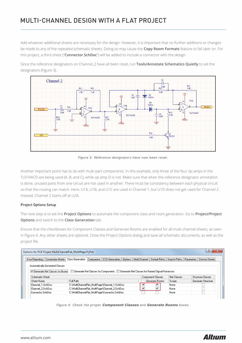
Since the reference designators on Channel_2 have all been reset, run Tools/Annotate Schematics Quietly to set the
designators (Figure 3).
Another important point has to do with multi-part components. In this example, only three of the four op amps in the
TL074ACD are being used (A, B, and C), while op amp D is not. Make sure that when the reference designator annotation
is done, unused parts from one circuit are not used in another. There must be consistency between each physical circuit
so that the routing can match. Here, U1A, U1B, and U1C are used in Channel 1, but U1D does not get used for Channel 2.
Instead, Channel 2 starts off at U2A.
Project Options Setup
The next step is to set the Project Options to automate the component class and room generation. Go to Project/Project
Options and switch to the Class Generation tab.
Ensure that the checkboxes for Component Classes and Generate Rooms are enabled for all multi-channel sheets, as seen
in Figure 4. Any other sheets are optional. Close the Project Options dialog and save all schematic documents, as well as the
project fi le.
Figure 3: Reference designators have now been reset.
Figure 4: Check the proper Component Classes and Generate Rooms boxes.
www.altium.com
MULTI-CHANNEL DESIGN WITH A FLAT PROJECT
PCB LAYOUT
Create and save a new PCB fi le, then use Design/Import Changes… to
populate the board. Ensure that the ECO includes the creation of the
Component Classes and Rooms (Figure 5). If not, recheck the Project
Options setup done previously.
The PCB will then be populated with the Rooms as shown in Figure 6.
Next, move the Channel_1 Room into the board area, then place and route it as desired. Resize the Room outline if
necessary (Figure 7).
Note: The following section detailing the
creation of a Design Channel Class is
optional when the circuit only needs to
be repeated a couple of times. The Copy
Room Formats command will operate
correctly when copying a single Room
format to another, as is the case in this
example. If the Room’s format needs
to be copied to subsequent Rooms,
however, the command will have to be
issued multiple times. It is, therefore,
a best-practice to create the Design
Channel Class as detailed here.
The next part of the process is to use the Copy Room Formats feature to replicate the placement and routing. Before that
happens, however, you must inform Altium Designer that Channel_1 and Channel_2 are the same circuit type. This is done by
creating a Design Channel Class.
Figure 5: Create the Component Classes and Rooms.
Figure 6: The PCB has been populated with Rooms.
Figure 7: You can resize the Room to see more detail.

www.altium.com
MULTI-CHANNEL DESIGN WITH A FLAT PROJECT
When a hierarchical structure is used to replicate circuits, the system inherently knows that the circuits are the same, based
on the fact that the sheet symbol references the same circuit multiple times. Since these circuits were merely copied and
pasted, the information is not automatically created. It is possible that one of the circuits was modifi ed by the user so that
there is no longer a match between them. If this is the case, the replication of layout information may not be possible. Since
no modifi cations were made to either circuit in this case, the replication can proceed.
Go to the Design/Classes menu. Note that there is a Component Class for each channel. These were automatically created
via the Project Options setting and are also used to defi ne the contents of each Room. Near the bottom of the Object
Classes list is an entry for “Design Channel Classes.” Right-click on that group and select Add Class. This creates an item
called “New Class.” Right-click the “New Class” name, select Rename Class, and change the name to “Circuit_1.” This renaming
step is optional, but if there is more than one circuit type being replicated, it will make it easier to keep track of them.
The members of a Design Channel Class are called Component Classes. Note that the “Channel_1” and “Channel_2”
Component Classes are listed in the Non-Members list. Select them both and click the arrow, to move them to the
Members list, shown in Figure 8.
Then, close the dialog. Set the board’s display so that both Rooms are visible. Go to Design/Rooms/Copy Room Formats.
The cursor will now change to a large cross-hair, and the Status Bar will instruct you to choose the Source Room. Click
anywhere inside the Channel_1 Room. The Status Bar then instructs you to choose the Destination Room. Click anywhere
inside the Channel_2 Room. The Confi rm Channel Format Copy dialog will then open and present several copying options,
as well as a list of all Rooms in the Design Channel Class that are available to copy to. Ensure that Channel_2 has the Copy
checkbox enabled. If not, the Apply to Specifi ed Channels checkbox may need to be enabled to access the Copy checkbox.
Figure 8: Move Channel_1 and Channel_2 to the Members list.
www.altium.com
MULTI-CHANNEL DESIGN WITH A FLAT PROJECT
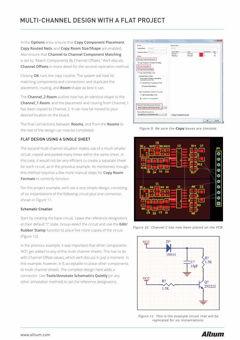
In the Options area, ensure that Copy Component Placement,
Copy Routed Nets, and Copy Room Size/Shape are enabled.
Also ensure that Channel to Channel Component Matching
is set to, “Match Components By Channel Off sets.” We’ll discuss
Channel Off sets in more detail for the second replication method.
Clicking OK runs the copy routine. The system will look for
matching components and connections and duplicate the
placement, routing, and Room shape as best it can.
The Channel_2 Room outline now has an identical shape to the
Channel_1 Room, and the placement and routing from Channel_1
has been copied to Channel_2. It can now be moved to your
desired location on the board.
The fi nal connections between Rooms, and from the Rooms to
the rest of the design can now be completed.
FLAT DESIGN USING A SINGLE SHEET
The second multi-channel situation makes use of a much smaller
circuit, copied and pasted many times within the same sheet. In
this case, it would not be very effi cient to create a separate sheet
for each circuit, as in the previous example. As mentioned, though,
this method requires a few more manual steps for Copy Room
Formats to correctly function.
For this project example, we’ll use a very simple design, consisting
of six instantiations of the following circuit plus one connector,
shown in Figure 11.
Schematic Creation
Start by creating the base circuit. Leave the reference designators
at their default “?” state. Group-select the circuit and use the Edit/
Rubber Stamp function to place fi ve more copies of the circuit
(Figure 12).
In the previous example, it was important that other components
NOT get added to any of the multi-channel sheets. This has to do
with Channel Off set values, which we’ll discuss in just a moment. In
this example, however, it IS acceptable to place other components
to multi-channel sheets. The complete design here adds a
connector. Use Tools/Annotate Schematics Quietly (or any
other annotation method) to set the reference designators.
Figure 9: Be sure the Copy boxes are checked.
Figure 10: Channel 2 has now been placed on the PCB.
Figure 11: This is the example circuit that will be replicated for six instantiations.

www.altium.com
MULTI-CHANNEL DESIGN WITH A FLAT PROJECT
Channel Offset Values
Before continuing with the next step, the concept of a
channel off set needs to be introduced. The main way
the Copy Room Formats function attempts to match
components from Room to Room is by checking if two
components share the same channel off set. This is
an integer value that Altium Designer places on each
component as it is passed to the PCB, and it is essentially
the component’s relative physical position within the
schematic sheet.
In the previous example, the Channel Off set values
(accessible in the PCB document, in a component’s
Properties) for Q1 and Q2 match (Figure 13).
They match because the circuits on the Channel_1 and
Channel_2 sheets are identical, so the positions of Q1
and Q2 are the same on each sheet. Figure 14 shows the
Channel Off sets match for each like component in Channel_1 and Channel_2.
Figure 12: The Edit/Rubber Stamp function reproduces the circuit fi ve times.
Figure 13: Note that the Channel Off set values are the same for both transistors (Q1 and Q2).

www.altium.com
MULTI-CHANNEL DESIGN WITH A FLAT PROJECT
Channel Off set values are sequentially applied to all components on a schematic. On the single sheet example, all
components will thus get unique Channel Off set values. However, that will not allow Copy Room Formats to match
components from circuit to circuit. Therefore, the Channel Off set values will need to be manually adjusted within the PCB
fi le. This is easy to do, but it is important to keep the relative order of the components within the copied circuits as they were
and not make any changes to their placement or reference designators. We’ll get more into that later.
Component Class Creation
With the multi-sheet method, Component Classes for the replicated circuits were created automatically, because of the
settings in Project Options. With a single sheet, the automated class would include all of the components on the page.
However, the Rooms need to be based on just the individual circuits. Therefore, the Component Classes must be manually
created on the schematic sheet.
A user-defi ned Component Class is created by adding a parameter to each component called “ClassName,” with the value
being the name of the class as it will appear in the PCB. Of course, editing the properties of each and every component in the
schematic would take some time. Altium Designer has a couple of options to add the “ClassName” parameter information to
groups of components, and both will be used here for demonstration purposes.
Go to Tools/Parameter Manager. Set the Options dialog to include only the
Parameters owned by “Parts.” Click Add Column… to add a new Parameter to every
component in the design. Enter “ClassName” In the Name fi eld and enable the Add to
all objects checkbox. Leave the Value fi eld blank.
Click Accept Changes (Create ECO) then click Execute Changes to complete the
addition of the parameters. Click Close to dismiss the ECO dialog.
Now each circuit will need to be labeled with a unique ClassName, so they each create
their own Component Class in the PCB. Group-select the entire fi rst circuit. Open the
SCH Inspector panel (View/Workspace Panels/SCH/SCH Inspector or F11). Pin the
panel in place. Set the fi lter at the top of the panel to “Include only Parts from current document”.
Figure 14: The Channel Off set values are shown next to each component in red. Note how they are identical for Channel 1 and Channel 2.
Figure 15: Name the parameter “ClassName” and check
Add to all objects.
www.altium.com
MULTI-CHANNEL DESIGN WITH A FLAT PROJECT
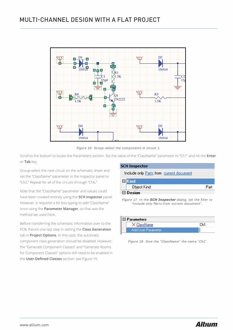
Scroll to the bottom to locate the Parameters section. Set the value of the “ClassName” parameter to “Ch1” and hit the Enter
or Tab key.
Group-select the next circuit on the schematic sheet and
set the “ClassName” parameter in the Inspector panel to
“Ch2.” Repeat for all of the circuits through “Ch6.”
Note that the “ClassName” parameter and values could
have been created entirely using the SCH Inspector panel.
However, it required a bit less typing to add “ClassName”
once using the Parameter Manager, so that was the
method we used here.
Before transferring the schematic information over to the
PCB, there’s one last step in setting the Class Generation
tab in Project Options. In this case, the automatic
component class generation should be disabled. However,
the “Generate Component Classes” and “Generate Rooms
for Component Classes” options still need to be enabled in
the User-Defi ned Classes section: see Figure 19.
Figure 16: Group-select the components in circuit 1.
Figure 17: In the SCH Inspector dialog, set the fi lter to “Include only Parts from current document”.
Figure 18: Give the “ClassName” the name “Ch1”.

www.altium.com
MULTI-CHANNEL DESIGN WITH A FLAT PROJECT
PCB Layout
Create and save a new PCB fi le, then use Design/Import Changes… to populate the board. Make sure that the ECO includes
the creation of the “Component Classes” and
Rooms. If it doesn’t, close the ECO dialog
without executing and recheck the existence
of the “ClassName” parameters and the Project
Options setup done previously.
Next, open the PCB panel (View/Workspace
Panels/PCB/PCB), and set the pull-down fi lter
to Components. Enable the Select checkbox.
The Component Classes area should show the “Ch1” through “Ch6” classes. Select
the “Ch1” class and notice that the contents are components from the Ch1 circuit on
the schematic (enabling Tools/Cross Select Mode in the PCB editor will also select the
components in the schematic document, if opened).
The components and their associated Rooms will be stacked outside the bottom right of
the board area. Use Design/Rooms/Move Room to spread the Rooms apart, or simply
click and drag the mouse inside the Room boundary (but not on a component body).
Figure 19: The Component Classes box has been unchecked. Leave the “Generate Component Classes” and “Generate Rooms for Component Classes” enabled (checked).
Figure 20: If not already checked, check the “ClassName” parameters.
Figure 21: Selecting “Ch1” reveals the components assigned to channel 1.

www.altium.com
MULTI-CHANNEL DESIGN WITH A FLAT PROJECT
Setting the Channel Offset Values
The next step is crucial to this process: setting the Channel Off set values. As previously mentioned, the Copy Room
Formats function will only fi nd like components whose Channel Off sets match. This needs to be done manually.
Using the PCB panel as mentioned above, make sure that the “select” checkbox is enabled, then select the “Ch1” class. Next,
open the PCB List panel (View/Workspace Panels/PCB/PCB List) and set the top fi lter to Edit selected objects Include
only Components.
Sort the list by the reference designator by clicking the
“Name” fi eld header. C1 should now appear at the top
of the list. Click in the “Channel Off set” cell for C1, type a
0 (zero) and hit Enter. This will set C1’s Channel Off set
value to 0 and bring you down to the next component
(D1). Type 1, then hit Enter and continue down the list,
until all components are sequentially numbered.
Leaving the PCB List panel open, return to the PCB panel
and select the “Ch2” class. The components from that
class should now populate the List panel. Again, sort the
list by reference designator by clicking the “Name” fi eld
header. Sorting the components this way will ensure
that the Channel Off set values will be the same for the
matching components in each circuit. Use the same
Channel Off set values as for the Ch1 components, as in
Figure 24.
Be sure to start numbering at 0 and continue
sequentially. Copy Room Formats can deal with non-
sequential values, but it will display a warning during the
process, so it’s best just to avoid it in the fi rst place.
Figure 22: Set the fi lter in the PCB List to Edit selected objects Include only Components.
Figure 23: Set the Channel Off set values manually to sequential numbers.
Figure 24: Continue for the rest of the channels.

www.altium.com
MULTI-CHANNEL DESIGN WITH A FLAT PROJECT
Repeat this process until the Channel Off sets for all 6 groups have been set. Being able to type directly in the List panel
makes this process quick; it takes just seconds to set all the values. For larger circuits, it may be helpful to point out that
external data can be pasted to multiple cells at once. This means that, for example, a spreadsheet can be used to quickly
create a long column of integers: enter a 0 in a cell then CTRL+drag the corner handle to auto-increment. Copy the cells in
the spreadsheet, select multiple cells in the Altium Designer List panel, then right-click and select Paste.
The last thing that needs to be done before laying out the circuit is to create the Design Channel Class in the same manner
that was done for the multi-sheet method. Go to Design/Classes, right-click the “Design Channel Classes” group, select “Add
Class,” and rename it “Circuit_2.” Select “Ch1” through “Ch6” and move them to the Members list. Close the dialog.
Layout and Copy Rooms
Locate the “Ch1” Room and move it into the board area. Click to select the Room
and use the sizing handles to make it a small square or rectangle. Place Ch1’s
components inside the Room and route the connections. The VCC and GND nets
were left as fanout vias here.
Now, all that’s left is to use the Copy Room Formats exactly as was done
the multi-sheet method on page 6 above. Go to Design/Rooms/Copy Room
Formats. Click the “Ch1” Room as the Source, then click any one of the remaining
Rooms as the Destination. Since they are all part of the same Channel Class,
the system will consider all of them as valid targets for the placement and routing
data. See Figure 27.
Figure 25: Add the channels to the Members list.
Figure 26: Here is the circuit after moving it to the PCB.

www.altium.com
MULTI-CHANNEL DESIGN WITH A FLAT PROJECT
In the Confi rm Channel Format Copy dialog, notice that all
six Rooms are presented. Ensure that the Apply To Specifi ed
Channels checkbox is enabled, and the Copy checkboxes are
enabled for all of the Rooms. Click OK to run the process. The
remaining fi ve Rooms should now be placed and routed exactly like
the fi rst Room.
Note: If a Channel-Off set Errors dialog pops up, it’s most likely
because the off set value changes made in the Setting the Channel
Off set Values section above were not done correctly. Check them
over again.
The Rooms can now be moved into place. This can be done
manually by dragging them, or by using Design/Rooms/Move
Room. Additionally, there’s an automated function to arrange them
evenly in a grid pattern. To run this process, fi rst select all of the
Rooms as shown in Figure 28.
Then, as shown in Figure 29, go to the Design/Rooms/Arrange
Rooms menu and set the number of columns and rows needed (in
this case, 2 rows of 3 columns). Other options are available to control
Room ordering, location, and spacing:
Figure 27: The fi nal step is to use the Copy Room Formats.
Figure 28: Before arranging, select all six Rooms.
Figure 29: Next, using the Design/Rooms/Arrange Rooms menu, set the number of
columns and rows needed (2x3).
www.altium.com
MULTI-CHANNEL DESIGN WITH A FLAT PROJECT
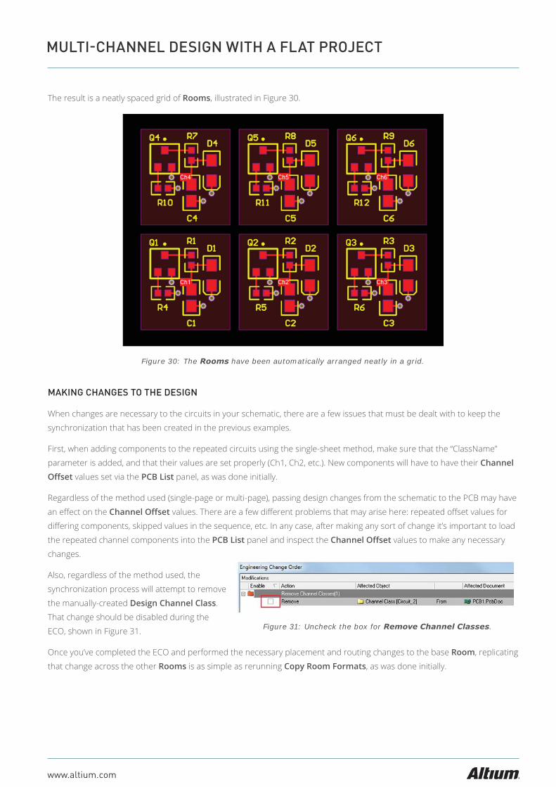
The result is a neatly spaced grid of Rooms, illustrated in Figure 30.
MAKING CHANGES TO THE DESIGN
When changes are necessary to the circuits in your schematic, there are a few issues that must be dealt with to keep the
synchronization that has been created in the previous examples.
First, when adding components to the repeated circuits using the single-sheet method, make sure that the “ClassName”
parameter is added, and that their values are set properly (Ch1, Ch2, etc.). New components will have to have their Channel
Off set values set via the PCB List panel, as was done initially.
Regardless of the method used (single-page or multi-page), passing design changes from the schematic to the PCB may have
an eff ect on the Channel Off set values. There are a few diff erent problems that may arise here: repeated off set values for
diff ering components, skipped values in the sequence, etc. In any case, after making any sort of change it’s important to load
the repeated channel components into the PCB List panel and inspect the Channel Off set values to make any necessary
changes.
Also, regardless of the method used, the
synchronization process will attempt to remove
the manually-created Design Channel Class.
That change should be disabled during the
ECO, shown in Figure 31.
Once you’ve completed the ECO and performed the necessary placement and routing changes to the base Room, replicating
that change across the other Rooms is as simple as rerunning Copy Room Formats, as was done initially.
Figure 30: The Rooms have been automatically arranged neatly in a grid.
Figure 31: Uncheck the box for Remove Channel Classes.
www.altium.com
MULTI-CHANNEL DESIGN WITH A FLAT PROJECT
CHECKLIST
Even after learning the above processes, it still may be helpful to have a checklist nearby to ensure that you don’t miss any
steps.
Flat Design Using Multiple Sheets
In SCH Inspector: Select, copy and paste the circuit from the source sheet to the target sheet(s)
Annotate reference designators, ensuring that multi-part components are unique to each sheet
In the Class Generation tab of Project Options, enable Component Classes and Generate Rooms for all sheets
that have the repeated circuit
In PCB: Import the design as usual. Move one Room to the PCB, then place & route the components in that Room
In Design/Classes, create a Design Channel Class and add to it the Component Classes that were auto-generated
for each sheet that has the repeated circuit
Use Design/Rooms/Copy Room Formats
Flat Design Using a Single Sheet
In SCH Inspector: Select the circuit and use Edit/Rubber Stamp to replicate the circuit
Annotate reference designators
Use Tools/Parameter Manager to add the “ClassName” parameter to all components
Select circuits individually and set the unique “ClassName” parameters (“Ch1”, “Ch2”, etc.) using the PCB Inspector
In the Class Generation tab of Project Options, disable Auto-Generated Component Classes, and enable
User-Defi ned Component Classes and Room generation
In PCB: Import design as usual
Open the PCB panel in Components view and enable Select mode
Select Component Class for fi rst channel
Open the PCB List panel in “Edit Selected Objects” mode
Sort the components list by reference designator, then set the Channel Off set values for all components
sequentially starting at 0
Go back to the PCB panel, select the next Component Class and repeat the Channel Off set value step. Do this for
all channels.
In Design/Classes, create a “Design Channel Class” and add the Component Classes for the repeated channels
Move one Room to the PCB, then place and route the components in that Room
Use Design/Rooms/Copy Room Formats