Embed Size (px)
Citation preview
8/11/2019 Mt 48lc2m32b2 - 64mb x32 Sdram
http://slidepdf.com/reader/full/mt-48lc2m32b2-64mb-x32-sdram 1/53
164Mb: x32 SDRAM Micron Technology, Inc., reserves the right to change products or specifications without notice.
64MSDRAMx32_5.p65 – Rev. B; Pub. 6/02 ©2002, Micron Technology, Inc.
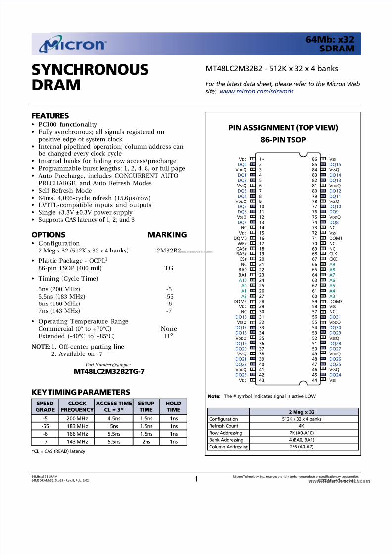
64Mb: x32SDRAM
2 Meg x 32
Configuration 512K x 32 x 4 banks
Refresh Count 4K
Row Addressing 2K (A0-A10)
Bank Addressing 4 (BA0, BA1)
Column Addressing 256 (A0-A7)
PIN ASSIGNMENT (TOP VIEW)
86-PIN TSOP
FEATURES PC100 functionality • Fully synchronous; all signals registered on
positive edge of system clock • Internal pipelined operation; column address can
be changed every clock cycle• Internal banks for hiding row access/precharge• Programmable burst lengths: 1, 2, 4, 8, or full page• Auto Precharge, includes CONCURRENT AUTO
PRECHARGE, and Auto Refresh Modes• Self Refresh Mode• 64ms, 4,096-cycle refresh (15.6µs/row)• LVTTL-compatible inputs and outputs• Single +3.3V ±0.3V power supply • Supports CAS latency of 1, 2, and 3
OPTIONS MARKING• Configuration
2 Meg x 32 (512K x 32 x 4 banks) 2M32B2
• Plastic Package - OCPL1
86-pin TSOP (400 mil) TG
• Timing (Cycle Time)
5ns (200 MHz) -55.5ns (183 MHz) -556ns (166 MHz) -67ns (143 MHz) -7
• Operating Temperature RangeCommercial (0° to +70°C) NoneExtended (-40°C to +85°C) IT2
NOTE: 1. Off-center parting line2. Available on -7
Part Number Example:
MT48LC2M32B2TG-7
Note: The # symbol indicates signal is active LOW.
VDD
DQ0VDDQDQ1DQ2VSSQDQ3
DQ4VDDQDQ5DQ6VSSQDQ7
NCVDD
DQM0WE#
CAS#RAS#
CS#NC
BA0BA1A10A0
A1A2DQM2
VDD
NCDQ16VSSQ
DQ17DQ18VDDQDQ19DQ20VSSQ
DQ21DQ22VDDQDQ23
VDD
1234567
8910111213141516171819202122232425
262728293031323334353637383940414243
86858483828180
797877767574737271706968676665646362
616059585756555453525150494847464544
VSS
DQ15VSSQDQ14DQ13VDDQDQ12
DQ11VSSQDQ10DQ9VDDQDQ8NCVSS
DQM1NCNCCLKCKEA9A8A7A6A5
A4A3DQM3VSS
NCDQ31VDDQDQ30DQ29VSSQDQ28DQ27VDDQDQ26DQ25VSSQDQ24VSS
SYNCHRONOUSDRAM
MT48LC2M32B2 - 512K x 32 x 4 banks
For the latest data sheet, please refer to the Micron Web site: www.micron.com/sdramds
KEY TIMING PARAMETERS
SPEED CLOCK ACCESS TIME SETUP HOLDGRADE FREQUENCY CL = 3* TIME TIME
-5 200 MHz 4.5ns 1.5ns 1ns
-55 183 MHz 5ns 1.5ns 1ns
-6 166 MHz 5.5ns 1.5ns 1ns
-7 143 MHz 5.5ns 2ns 1ns
*CL = CAS (READ) latency
8/11/2019 Mt 48lc2m32b2 - 64mb x32 Sdram
http://slidepdf.com/reader/full/mt-48lc2m32b2-64mb-x32-sdram 2/53
264Mb: x32 SDRAM Micron Technology, Inc., reserves the right to change products or specifications without notice.
64MSDRAMx32_5.p65 – Rev. B; Pub. 6/02 ©2002, Micron Technology, Inc.
64Mb: x32SDRAM
The SDRAM provides for programmable READ or WRITE burst lengths of 1, 2, 4, or 8 locations, or the fullpage, with a burst terminate option. An auto prechargefunction may be enabled to provide a self-timed row
precharge that is initiated at the end of the burst se-quence.
The 64Mb SDRAM uses an internal pipelined archi-tecture to achieve high-speed operation. This archi-tecture is compatible with the 2n rule of prefetch archi-tectures, but it also allows the column address to bechanged on every clock cycle to achieve a high-speed,fully random access. Precharging one bank while ac-cessing one of the other three banks will hide theprecharge cycles and provide seamless, high-speed,random-access operation.
The 64Mb SDRAM is designed to operate in 3.3V,low-power memory systems. An auto refresh mode is
provided, along with a power-saving, power-downmode. All inputs and outputs are LVTTL-compatible.SDRAMs offer substantial advances in DRAM oper-
ating performance, including the ability to synchro-nously burst data at a high data rate with automaticcolumn-address generation, the ability to interleavebetween internal banks to hide precharge time andthe capability to randomly change column addresseson each clock cycle during a burst access.
GENERAL DESCRIPTIONThe 64Mb SDRAM is a high-speed CMOS, dynamic
random-access memory containing 67,108,864-bits. Itis internally configured as a quad-bank DRAM with asynchronous interface (all signals are registered on thepositive edge of the clock signal, CLK). Each of the16,777,216-bit banks is organized as 2,048 rows by 256columns by 32 bits.
Read and write accesses to the SDRAM are burstoriented; accesses start at a selected location and con-tinue for a programmed number of locations in a pro-
grammed sequence. Accesses begin with the registra-tion of an ACTIVE command, which is then followed by a READ or WRITE command. The address bits regis-tered coincident with the ACTIVE command are usedto select the bank and row to be accessed (BA0, BA1select the bank, A0-A10 select the row). The addressbits registered coincident with the READ or WRITE com-mand are used to select the starting column locationfor the burst access.
64Mb (x32) SDRAM PART NUMBER
PART NUMBER ARCHITECTURE
MT48LC2M32B2TG 2 Meg x 32
8/11/2019 Mt 48lc2m32b2 - 64mb x32 Sdram
http://slidepdf.com/reader/full/mt-48lc2m32b2-64mb-x32-sdram 3/53
364Mb: x32 SDRAM Micron Technology, Inc., reserves the right to change products or specifications without notice.
64MSDRAMx32_5.p65 – Rev. B; Pub. 6/02 ©2002, Micron Technology, Inc.
64Mb: x32SDRAM
TABLE OF CONTENTS
Functional Block Diagram - 2 Meg x 32 ................. 4Pin Descriptions ..................................................... 5
Functional Description ......................................... 6Initialization ...................................................... 6Register Definition ............................................ 6
Mode Register ............................................... 6Burst Length............................................ 6Burst Type ............................................... 7CAS Latency ............................................ 8Operating Mode ...................................... 8Write Burst Mode .................................... 8
Commands ............................................................ 9Truth Table 1 (Commands and DQM Operation) ............ 9Command Inhibit ............................................. 10No Operation (NOP).......................................... 10
Load Mode Register ........................................... 10Active ................................................................ 10Read ................................................................ 10Write ................................................................ 10Precharge ........................................................... 10Auto Precharge .................................................. 10Burst Terminate ................................................. 11Auto Refresh ...................................................... 11Self Refresh ........................................................ 11
Operation ............................................................... 12Bank/Row Activation ........................................ 12Reads ................................................................ 13Writes ................................................................ 19Precharge ........................................................... 21Power-Down ...................................................... 21Clock Suspend .................................................. 22Burst Read/Single Write .................................... 22
Concurrent Auto Precharge .............................. 23Write with Auto Precharge ............................... 24
Truth Table 2 (CKE) ................................................ 25Truth Table 3 (Current State, Same Bank) ..................... 26Truth Table 4 (Current State, Different Bank) ................. 28
Absolute Maximum Ratings .................................. 30DC Electrical Characteristics
and Operating Conditions...................................... 30IDD Specifications and Conditions ......................... 30Capacitance ............................................................ 32
AC Electrical Characteristics (Timing Table) .... 32AC Electrical Characteristics ................................... 34
Timing WaveformsInitialize and Load Mode Register .................... 36Power-Down Mode .......................................... 37
Clock Suspend Mode ........................................ 38Auto Refresh Mode ........................................... 39Self Refresh Mode ............................................. 40Reads
Read – Single Read....................................... 41Read – Without Auto Precharge ................. 42Read – With Auto Precharge ....................... 43Alternating Bank Read Accesses .................. 44Read – Full-Page Burst ................................. 45Read – DQM Operation .............................. 46
WritesWrite – Single Write..................................... 47Write – Without Auto Precharge ................ 48
Write – With Auto Precharge ...................... 49Alternating Bank Write Accesses ................. 50Write – Full-Page Burst ................................ 51Write – DQM Operation ............................. 52
8/11/2019 Mt 48lc2m32b2 - 64mb x32 Sdram
http://slidepdf.com/reader/full/mt-48lc2m32b2-64mb-x32-sdram 4/53
464Mb: x32 SDRAM Micron Technology, Inc., reserves the right to change products or specifications without notice.
64MSDRAMx32_5.p65 – Rev. B; Pub. 6/02 ©2002, Micron Technology, Inc.
64Mb: x32SDRAM
FUNCTIONAL BLOCK DIAGRAM2 Meg x 32 SDRAM
11
RAS#
CAS#
CLK
CS#
WE#
CKE
8
A0-A10,BA0, BA1
DQM0-DQM3
13
256(x32)
8192
I/O GATINGDQM MASK LOGICREAD DATA LATCH
WRITE DRIVERS
COLUMNDECODER
BANK0MEMORY
ARRAY(2,048 x 256 x 32)
BANK0ROW-
ADDRESSLATCH
&DECODER
2048
SENSE AMPLIFIERS
BANKCONTROL
LOGIC
DQ0-DQ31
32
32
DATAINPUT
REGISTER
DATAOUTPUTREGISTER
32
BANK1BANK0
BANK2BANK3
11
8
2
4 4
2
REFRESHCOUNTER
11
11
MODE REGISTER
CONTROLLOGIC
C O M M A N D
D E C O D E
ROW-ADDRESS
MUX
ADDRESSREGISTER
COLUMN-ADDRESSCOUNTER/
LATCH
8/11/2019 Mt 48lc2m32b2 - 64mb x32 Sdram
http://slidepdf.com/reader/full/mt-48lc2m32b2-64mb-x32-sdram 5/53
564Mb: x32 SDRAM Micron Technology, Inc., reserves the right to change products or specifications without notice.
64MSDRAMx32_5.p65 – Rev. B; Pub. 6/02 ©2002, Micron Technology, Inc.
64Mb: x32SDRAM
PIN DESCRIPTIONS
PIN NUMBERS SYMBOL TYPE DESCRIPTION
68 CLK Input Clock: CLK is driven by the system clock. All SDRAM input signals are
sampled on the positive edge of CLK. CLK also increments the internal burstcounter and controls the output registers.
67 CKE Input Clock Enable: CKE activates (HIGH) and deactivates (LOW) the CLK signal.
Deactivating the clock provides PRECHARGE POWER-DOWN and SELF REFRESH
operation (all banks idle), ACTIVE POWER-DOWN (row active in any bank) or
CLOCK SUSPEND operation (burst/access in progress). CKE is synchronous
except after the device enters power-down and self refresh modes, where
CKE becomes asynchronous until after exiting the same mode. The input
buffers, including CLK, are disabled during power-down and self refresh
modes, providing low standby power. CKE may be tied HIGH.
20 CS# Input Chip Select: CS# enables (registered LOW) and disables (registered HIGH) the
command decoder. All commands are masked when CS# is registered HIGH.
CS# provides for external bank selection on systems with multiple banks.CS# is considered part of the command code.
17, 18, 19 WE#, CAS#, Input Command Inputs: WE# , CAS#, and RAS# (along with CS#) define the
RAS# command being entered.
16, 71, 28, 59 DQM0- Input Input/Output Mask: DQM is sampled HIGH and is an input mask signal
DQM3 for write accesses and an output enable signal for read accesses. Input data
is masked during a WRITE cycle. The output buffers are placed in a High-Z
state (two-clock latency) during a READ cycle. DQM0 corresponds to DQ0-
DQ7; DQM1 corresponds to DQ8-DQ15; DQM2 corresponds to DQ16-DQ23;
and DQM3 corresponds to DQ24-DQ31. DQM0-DQM3 are considered same
state when referenced as DQM.
22, 23 BA0, BA1 Input Bank Address Input(s): BA0 and BA1 define to which bank the ACTIVE, READ,
WRITE or PRECHARGE command is being applied.
25-27, 60-66, 24 A0-A10 Input Address Inputs: A0-A10 are sampled during the ACTIVE command (row-
address A0-A10) and READ/WRITE command (column-address A0-A7 with A10
defining auto precharge) to select one location out of the memory array in
the respective bank. A10 is sampled during a PRECHARGE command to
determine if all banks are to be precharged (A10 HIGH) or bank selected by
BA0, BA1 (LOW). The address inputs also provide the op-code during a LOAD
MODE REGISTER command.
2, 4, 5, 7, 8, 10, 11, 13, DQ0-DQ31 Input/ Data I/Os: Data bus.
74, 76, 77, 79, 80, 82, 83, Output
85, 31, 33, 34, 36, 37, 39,
40, 42, 45, 47, 48, 50, 51,
53, 54, 56
14, 21, 30, 57, 69, 70, 73 NC – No Connect: These pins should be left unconnected. Pin 70 is reservedfor SSTL reference voltage supply.
3, 9, 35, 41, 49, 55, 75, 81 VDDQ Supply DQ Power Supply: Isolated on the die for improved noise immunity.
6, 12, 32, 38, 46, 52, 78, 84 VSSQ Supply DQ Ground: Provide isolated ground to DQs for improved noise immunity.
1, 15, 29, 43 VDD Supply Power Supply: +3.3V ±0.3V. (See note 27 on page 35.)
44, 58, 72, 86 VSS Supply Ground.
8/11/2019 Mt 48lc2m32b2 - 64mb x32 Sdram
http://slidepdf.com/reader/full/mt-48lc2m32b2-64mb-x32-sdram 6/53
664Mb: x32 SDRAM Micron Technology, Inc., reserves the right to change products or specifications without notice.
64MSDRAMx32_5.p65 – Rev. B; Pub. 6/02 ©2002, Micron Technology, Inc.
64Mb: x32SDRAM
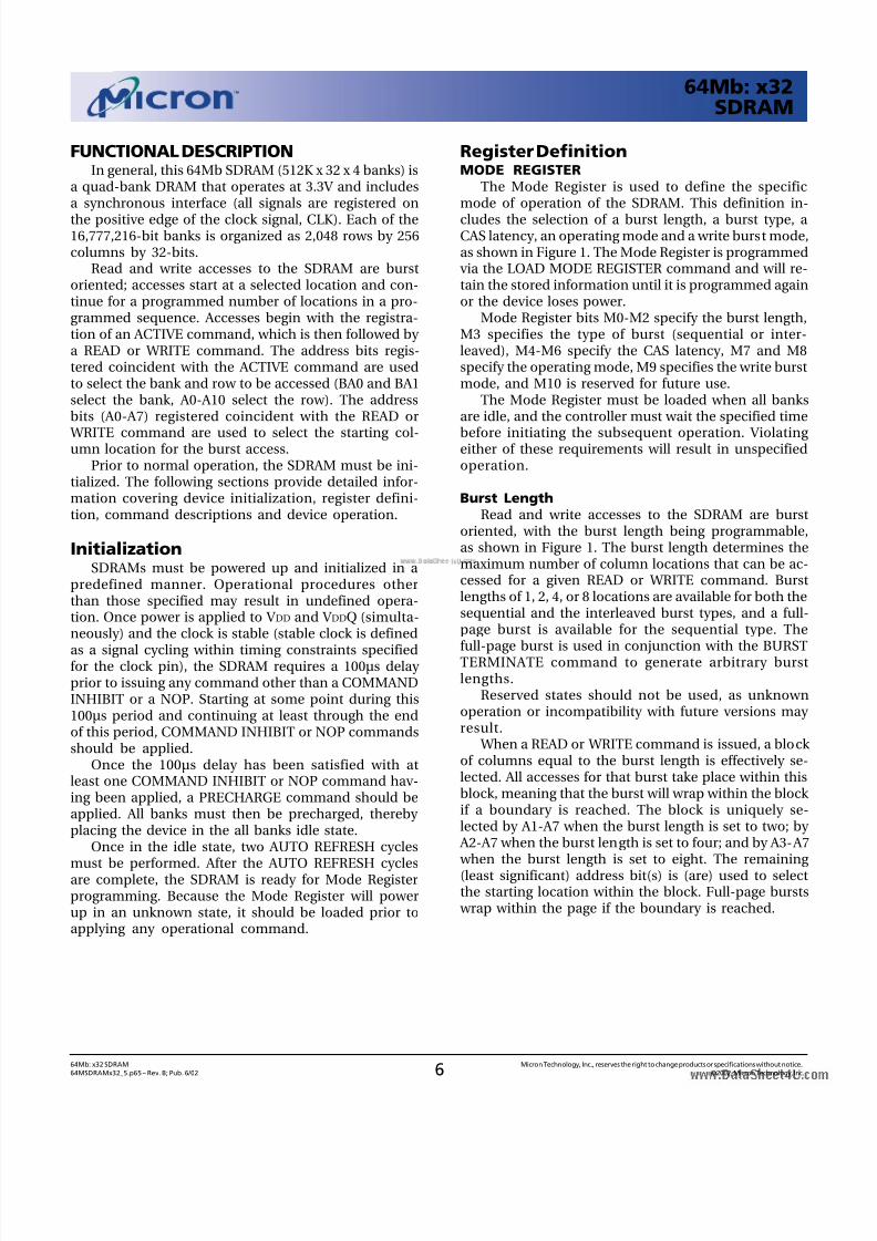
FUNCTIONAL DESCRIPTIONIn general, this 64Mb SDRAM (512K x 32 x 4 banks) is
a quad-bank DRAM that operates at 3.3V and includesa synchronous interface (all signals are registered on
the positive edge of the clock signal, CLK). Each of the16,777,216-bit banks is organized as 2,048 rows by 256columns by 32-bits.
Read and write accesses to the SDRAM are burstoriented; accesses start at a selected location and con-tinue for a programmed number of locations in a pro-grammed sequence. Accesses begin with the registra-tion of an ACTIVE command, which is then followed by a READ or WRITE command. The address bits regis-tered coincident with the ACTIVE command are usedto select the bank and row to be accessed (BA0 and BA1select the bank, A0-A10 select the row). The addressbits (A0-A7) registered coincident with the READ or
WRITE command are used to select the starting col-umn location for the burst access.
Prior to normal operation, the SDRAM must be ini-tialized. The following sections provide detailed infor-mation covering device initialization, register defini-tion, command descriptions and device operation.
InitializationSDRAMs must be powered up and initialized in a
predefined manner. Operational procedures otherthan those specified may result in undefined opera-tion. Once power is applied to V DD and V DDQ (simulta-neously) and the clock is stable (stable clock is defined
as a signal cycling within timing constraints specifiedfor the clock pin), the SDRAM requires a 100µs delay prior to issuing any command other than a COMMANDINHIBIT or a NOP. Starting at some point during this100µs period and continuing at least through the endof this period, COMMAND INHIBIT or NOP commandsshould be applied.
Once the 100µs delay has been satisfied with atleast one COMMAND INHIBIT or NOP command hav-ing been applied, a PRECHARGE command should beapplied. All banks must then be precharged, thereby placing the device in the all banks idle state.
Once in the idle state, two AUTO REFRESH cycles
must be performed. After the AUTO REFRESH cyclesare complete, the SDRAM is ready for Mode Registerprogramming. Because the Mode Register will powerup in an unknown state, it should be loaded prior toapplying any operational command.
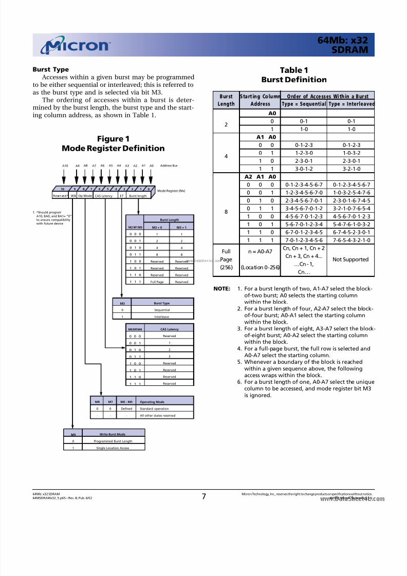
Register DefinitionMODE REGISTER
The Mode Register is used to define the specificmode of operation of the SDRAM. This definition in-
cludes the selection of a burst length, a burst type, aCAS latency, an operating mode and a write burst mode,as shown in Figure 1. The Mode Register is programmedvia the LOAD MODE REGISTER command and will re-tain the stored information until it is programmed againor the device loses power.
Mode Register bits M0-M2 specify the burst length,M3 specifies the type of burst (sequential or inter-leaved), M4-M6 specify the CAS latency, M7 and M8specify the operating mode, M9 specifies the write burstmode, and M10 is reserved for future use.
The Mode Register must be loaded when all banksare idle, and the controller must wait the specified time
before initiating the subsequent operation. Violating either of these requirements will result in unspecifiedoperation.
Burst LengthRead and write accesses to the SDRAM are burst
oriented, with the burst length being programmable,as shown in Figure 1. The burst length determines themaximum number of column locations that can be ac-cessed for a given READ or WRITE command. Burstlengths of 1, 2, 4, or 8 locations are available for both thesequential and the interleaved burst types, and a full-page burst is available for the sequential type. The
full-page burst is used in conjunction with the BURSTTERMINATE command to generate arbitrary burstlengths.
Reserved states should not be used, as unknownoperation or incompatibility with future versions may result.
When a READ or WRITE command is issued, a block of columns equal to the burst length is effectively se-lected. All accesses for that burst take place within thisblock, meaning that the burst will wrap within the block if a boundary is reached. The block is uniquely se-lected by A1-A7 when the burst length is set to two; by A2-A7 when the burst length is set to four; and by A3-A7 when the burst length is set to eight. The remaining (least significant) address bit(s) is (are) used to selectthe starting location within the block. Full-page bursts wrap within the page if the boundary is reached.
8/11/2019 Mt 48lc2m32b2 - 64mb x32 Sdram
http://slidepdf.com/reader/full/mt-48lc2m32b2-64mb-x32-sdram 7/53
764Mb: x32 SDRAM Micron Technology, Inc., reserves the right to change products or specifications without notice.
64MSDRAMx32_5.p65 – Rev. B; Pub. 6/02 ©2002, Micron Technology, Inc.
64Mb: x32SDRAM
NOTE: 1. For a burst length of two, A1-A7 select the block-of-two burst; A0 selects the starting column
within the block.2. For a burst length of four, A2-A7 select the block-
of-four burst; A0-A1 select the starting columnwithin the block.
3. For a burst length of eight, A3-A7 select the block-of-eight burst; A0-A2 select the starting columnwithin the block.
4. For a full-page burst, the full row is selected andA0-A7 select the starting column.
5. Whenever a boundary of the block is reachedwithin a given sequence above, the followingaccess wraps within the block.
6. For a burst length of one, A0-A7 select the uniquecolumn to be accessed, and mode register bit M3is ignored.
Table 1Burst Definition
Bur st Start ing Co lumn Order of Accesses With in a Bur st
Length Address Type = Sequential Type = Interleaved
A0
20 0-1 0-1
1 1-0 1-0
A1 A0
0 0 0-1-2-3 0-1-2-3
40 1 1-2-3-0 1-0-3-2
1 0 2-3-0-1 2-3-0-1
1 1 3-0-1-2 3-2-1-0
A2 A1 A0
0 0 0 0-1-2-3-4-5-6-7 0-1-2-3-4-5-6-7
0 0 1 1-2-3-4-5-6-7-0 1-0-3-2-5-4-7-6
0 1 0 2-3-4-5-6-7-0-1 2-3-0-1-6-7-4-5
80 1 1 3-4-5-6-7-0-1-2 3-2-1-0-7-6-5-4
1 0 0 4-5-6-7-0-1-2-3 4-5-6-7-0-1-2-3
1 0 1 5-6-7-0-1-2-3-4 5-4-7-6-1-0-3-2
1 1 0 6-7-0-1-2-3-4-5 6-7-4-5-2-3-0-1
1 1 1 7-0-1-2-3-4-5-6 7-6-5-4-3-2-1-0
Full n = A0-A7Cn, Cn + 1, Cn + 2
PageCn + 3, Cn + 4...
Not Supported
(256) (Location 0 -256)…Cn - 1,
Cn…
Figure 1Mode Register Definition
Burst Type Accesses within a given burst may be programmed
to be either sequential or interleaved; this is referred toas the burst type and is selected via bit M3.
The ordering of accesses within a burst is deter-mined by the burst length, the burst type and the start-ing column address, as shown in Table 1.
0 0 0
0 0 1
0 1 0
0 1 1
1 0 0
1 0 1
1 1 0
1 1 1
M3 = 0
1
2
4
8
Reserved
Reserved
Reserved
Full Page
M3 = 1
1
2
4
8
Reserved
Reserved
Reserved
Reserved
Operating Mode
Standard operation
All other states reserved
0
-
0
-
Defined
-
0
1
Burst Type
Sequential
Interleave
CAS Latency
Reserved
1
2
3
Reserved
Reserved
Reserved
Reserved
0 0 0
0 0 1
0 1 0
0 1 1
1 0 0
1 0 1
1 1 0
1 1 1
Burst Length
M0
Burst lengthCAS Latency BT
A9 A7 A6 A5 A4 A3A8 A2 A1 A0
Mode Register (Mx)
Address Bus
9 7 6 5 4 38 2 1 0
M1M2
M3
M4M5M6
M6 - M0M8 M7
Op Mode
A10
10
Reserved* WB
0
1
Write Burst Mode
Programmed Burst Length
Single Location Access
M9
1. *Should programA10, BA0, and BA1= “0”to ensure compatibilitywith future device
8/11/2019 Mt 48lc2m32b2 - 64mb x32 Sdram
http://slidepdf.com/reader/full/mt-48lc2m32b2-64mb-x32-sdram 8/53
864Mb: x32 SDRAM Micron Technology, Inc., reserves the right to change products or specifications without notice.
64MSDRAMx32_5.p65 – Rev. B; Pub. 6/02 ©2002, Micron Technology, Inc.
64Mb: x32SDRAM
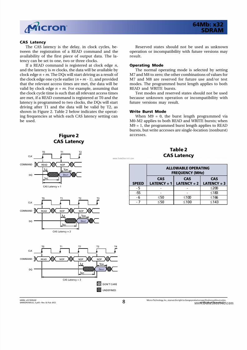
ALLOWABLE OPERATINGFREQUENCY (MHz)
CAS CAS CAS
SPEED LATENCY = 1 LATENCY = 2 LATENCY = 3- 5 - - ≤ 200
-55 - - ≤ 183
- 6 ≤ 50 ≤ 100 ≤ 166
- 7 ≤ 50 ≤ 100 ≤ 143
Reserved states should not be used as unknownoperation or incompatibility with future versions may result.
Operating ModeThe normal operating mode is selected by setting
M7 and M8 to zero; the other combinations of values forM7 and M8 are reserved for future use and/or testmodes. The programmed burst length applies to bothREAD and WRITE bursts.
Test modes and reserved states should not be usedbecause unknown operation or incompatibility withfuture versions may result.
Write Burst Mode When M9 = 0, the burst length programmed via
M0-M2 applies to both READ and WRITE bursts; whenM9 = 1, the programmed burst length applies to READbursts, but write accesses are single-location (nonburst)accesses.
CAS LatencyThe CAS latency is the delay, in clock cycles, be-
tween the registration of a READ command and theavailability of the first piece of output data. The la-
tency can be set to one, two or three clocks.If a READ command is registered at clock edge n,
and the latency is m clocks, the data will be available by clock edge n + m. The DQs will start driving as a result of the clock edge one cycle earlier (n + m - 1), and providedthat the relevant access times are met, the data will bevalid by clock edge n + m. For example, assuming thatthe clock cycle time is such that all relevant access timesare met, if a READ command is registered at T0 and thelatency is programmed to two clocks, the DQs will startdriving after T1 and the data will be valid by T2, asshown in Figure 2. Table 2 below indicates the operat-ing frequencies at which each CAS latency setting can
be used.
Figure 2CAS Latency
Table 2CAS Latency
CLK
DQ
T2T1 T3T0
CAS Latency = 3
LZ
DOUT
tOHt
COMMAND NOPREAD
tAC
NOP
T4
NOP
DON’T CARE
UNDEFINED
CLK
DQ
T2T1T0
CAS Latency = 1
LZ
DOUT
tOHt
COMMAND NOPREAD
tAC
CLK
DQ
T2T1 T3T0
CAS Latency = 2
LZ
DOUT
tOHt
COMMAND NOPREAD
tAC
NOP
8/11/2019 Mt 48lc2m32b2 - 64mb x32 Sdram
http://slidepdf.com/reader/full/mt-48lc2m32b2-64mb-x32-sdram 9/53
964Mb: x32 SDRAM Micron Technology, Inc., reserves the right to change products or specifications without notice.
64MSDRAMx32_5.p65 – Rev. B; Pub. 6/02 ©2002, Micron Technology, Inc.
64Mb: x32SDRAM
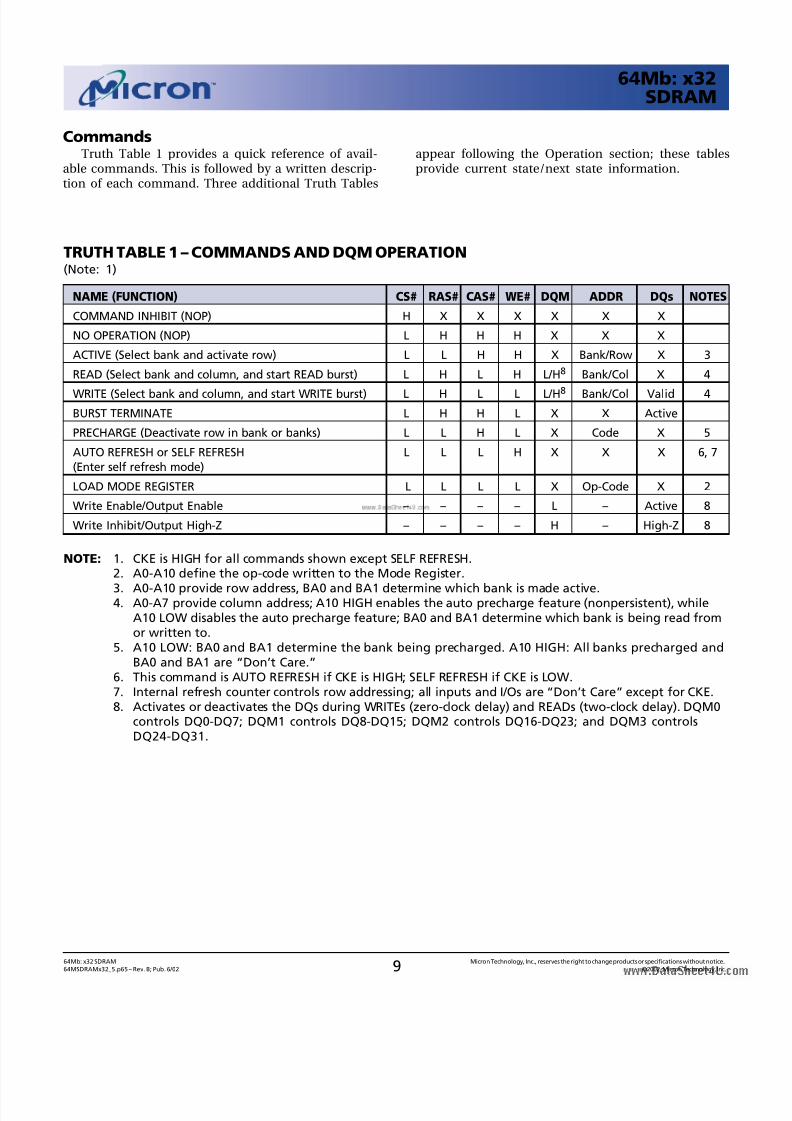
TRUTH TABLE 1 – COMMANDS AND DQM OPERATION(Note: 1)
NAME (FUNCTION) CS# RAS# CAS# WE# DQM ADDR DQs NOTES
COMMAND INHIBIT (NOP) H X X X X X X
NO OPERATION (NOP) L H H H X X X
ACTIVE (Select bank and activate row) L L H H X Bank/Row X 3
READ (Select bank and column, and start READ burst) L H L H L/H8 Bank/Col X 4
WRITE (Select bank and column, and start WRITE burst) L H L L L/H8 Bank/Col Valid 4
BURST TERMINATE L H H L X X Active
PRECHARGE (Deactivate row in bank or banks) L L H L X Code X 5
AUTO REFRESH or SELF REFRESH L L L H X X X 6, 7
(Enter self refresh mode)
LOAD MODE REGISTER L L L L X Op-Code X 2
Write Enable/Output Enable – – – – L – Active 8
Write Inhibit/Output High-Z – – – – H – High-Z 8
appear following the Operation section; these tablesprovide current state/next state information.
CommandsTruth Table 1 provides a quick reference of avail-
able commands. This is followed by a written descrip-tion of each command. Three additional Truth Tables
NOTE: 1. CKE is HIGH for all commands shown except SELF REFRESH.2. A0-A10 define the op-code written to the Mode Register.
3. A0-A10 provide row address, BA0 and BA1 determine which bank is made active.4. A0-A7 provide column address; A10 HIGH enables the auto precharge feature (nonpersistent), while
A10 LOW disables the auto precharge feature; BA0 and BA1 determine which bank is being read fromor written to.
5. A10 LOW: BA0 and BA1 determine the bank being precharged. A10 HIGH: All banks precharged andBA0 and BA1 are “Don’t Care.”
6. This command is AUTO REFRESH if CKE is HIGH; SELF REFRESH if CKE is LOW.7. Internal refresh counter controls row addressing; all inputs and I/Os are “Don’t Care” except for CKE.8. Activates or deactivates the DQs during WRITEs (zero-clock delay) and READs (two-clock delay). DQM0
controls DQ0-DQ7; DQM1 controls DQ8-DQ15; DQM2 controls DQ16-DQ23; and DQM3 controlsDQ24-DQ31.
8/11/2019 Mt 48lc2m32b2 - 64mb x32 Sdram
http://slidepdf.com/reader/full/mt-48lc2m32b2-64mb-x32-sdram 10/53
1064Mb: x32 SDRAM Micron Technology, Inc., reserves the right to change products or specifications without notice.
64MSDRAMx32_5.p65 – Rev. B; Pub. 6/02 ©2002, Micron Technology, Inc.
64Mb: x32SDRAM
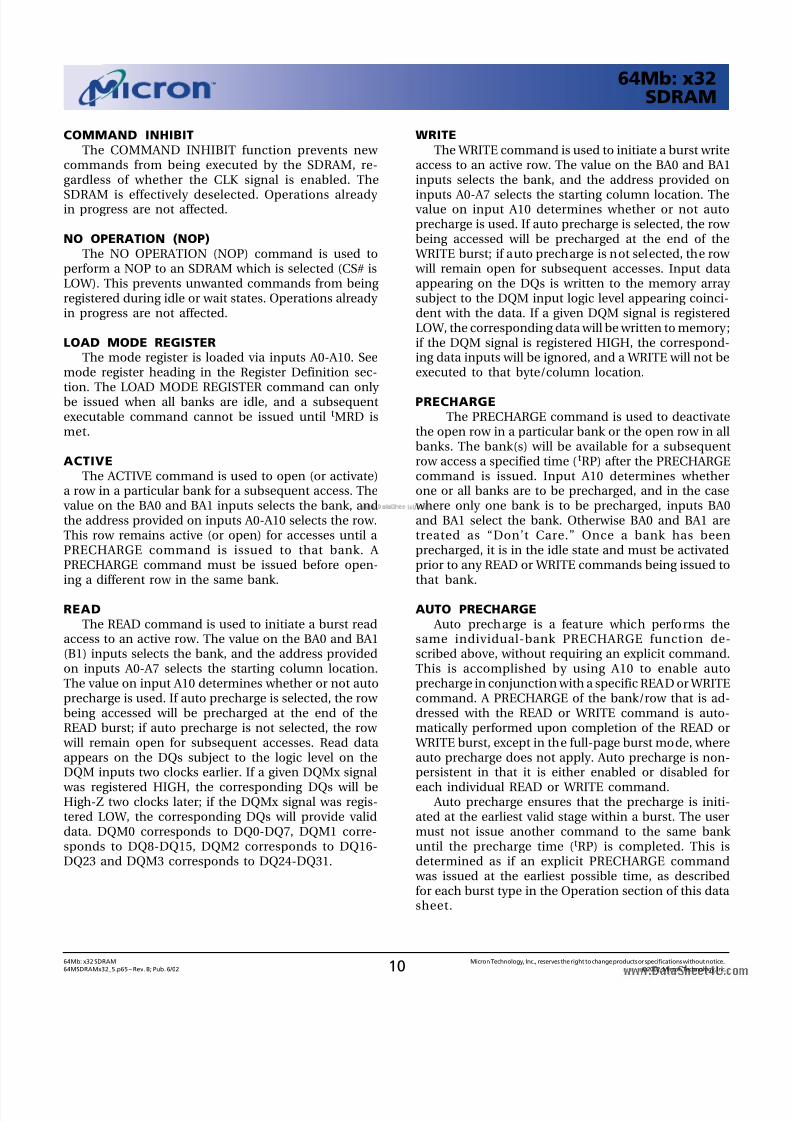
COMMAND INHIBITThe COMMAND INHIBIT function prevents new
commands from being executed by the SDRAM, re-gardless of whether the CLK signal is enabled. The
SDRAM is effectively deselected. Operations already in progress are not affected.
NO OPERATION (NOP)The NO OPERATION (NOP) command is used to
perform a NOP to an SDRAM which is selected (CS# isLOW). This prevents unwanted commands from being registered during idle or wait states. Operations already in progress are not affected.
LOAD MODE REGISTERThe mode register is loaded via inputs A0-A10. See
mode register heading in the Register Definition sec-
tion. The LOAD MODE REGISTER command can only be issued when all banks are idle, and a subsequentexecutable command cannot be issued until tMRD ismet.
ACTIVEThe ACTIVE command is used to open (or activate)
a row in a particular bank for a subsequent access. Thevalue on the BA0 and BA1 inputs selects the bank, andthe address provided on inputs A0-A10 selects the row.This row remains active (or open) for accesses until aPRECHARGE command is issued to that bank. A PRECHARGE command must be issued before open-ing a different row in the same bank.
READThe READ command is used to initiate a burst read
access to an active row. The value on the BA0 and BA1(B1) inputs selects the bank, and the address providedon inputs A0-A7 selects the starting column location.The value on input A10 determines whether or not autoprecharge is used. If auto precharge is selected, the row being accessed will be precharged at the end of theREAD burst; if auto precharge is not selected, the row will remain open for subsequent accesses. Read dataappears on the DQs subject to the logic level on theDQM inputs two clocks earlier. If a given DQMx signal
was registered HIGH, the corresponding DQs will beHigh-Z two clocks later; if the DQMx signal was regis-tered LOW, the corresponding DQs will provide validdata. DQM0 corresponds to DQ0-DQ7, DQM1 corre-sponds to DQ8-DQ15, DQM2 corresponds to DQ16-DQ23 and DQM3 corresponds to DQ24-DQ31.
WRITEThe WRITE command is used to initiate a burst write
access to an active row. The value on the BA0 and BA1inputs selects the bank, and the address provided on
inputs A0-A7 selects the starting column location. Thevalue on input A10 determines whether or not autoprecharge is used. If auto precharge is selected, the row being accessed will be precharged at the end of the WRITE burst; if auto precharge is not selected, the row will remain open for subsequent accesses. Input dataappearing on the DQs is written to the memory array subject to the DQM input logic level appearing coinci-dent with the data. If a given DQM signal is registeredLOW, the corresponding data will be written to memory;if the DQM signal is registered HIGH, the correspond-ing data inputs will be ignored, and a WRITE will not beexecuted to that byte/column location.
PRECHARGEThe PRECHARGE command is used to deactivate
the open row in a particular bank or the open row in allbanks. The bank(s) will be available for a subsequentrow access a specified time (tRP) after the PRECHARGEcommand is issued. Input A10 determines whetherone or all banks are to be precharged, and in the case where only one bank is to be precharged, inputs BA0and BA1 select the bank. Otherwise BA0 and BA1 aretreated as “Don’t Care.” Once a bank has beenprecharged, it is in the idle state and must be activatedprior to any READ or WRITE commands being issued tothat bank.
AUTO PRECHARGE Auto precharge is a feature which performs the
same individual-bank PRECHARGE function de-scribed above, without requiring an explicit command.This is accomplished by using A10 to enable autoprecharge in conjunction with a specific READ or WRITEcommand. A PRECHARGE of the bank/row that is ad-dressed with the READ or WRITE command is auto-matically performed upon completion of the READ or WRITE burst, except in the full-page burst mode, whereauto precharge does not apply. Auto precharge is non-persistent in that it is either enabled or disabled for
each individual READ or WRITE command. Auto precharge ensures that the precharge is initi-
ated at the earliest valid stage within a burst. The usermust not issue another command to the same bank until the precharge time (tRP) is completed. This isdetermined as if an explicit PRECHARGE command was issued at the earliest possible time, as describedfor each burst type in the Operation section of this datasheet.
8/11/2019 Mt 48lc2m32b2 - 64mb x32 Sdram
http://slidepdf.com/reader/full/mt-48lc2m32b2-64mb-x32-sdram 11/53
1164Mb: x32 SDRAM Micron Technology, Inc., reserves the right to change products or specifications without notice.
64MSDRAMx32_5.p65 – Rev. B; Pub. 6/02 ©2002, Micron Technology, Inc.
64Mb: x32SDRAM
BURST TERMINATEThe BURST TERMINATE command is used to trun-
cate either fixed-length or full-page bursts. The mostrecently registered READ or WRITE command prior to
the BURST TERMINATE command will be truncated,as shown in the Operation section of this data sheet.
AUTO REFRESH AUTO REFRESH is used during normal operation of
the SDRAM and is analagous to CAS#-BEFORE-RAS#(CBR) REFRESH in conventional DRAMs. This com-mand is nonpersistent, so it must be issued each timea refresh is required.
The addressing is generated by the internal refreshcontroller. This makes the address bits “Don’t Care”during an AUTO REFRESH command. The 64MbSDRAM requires 4,096 AUTO REFRESH cycles every
64ms (t
REF), regardless of width option. Providing adistributed AUTO REFRESH command every 15.625µs will meet the refresh requirement and ensure that eachrow is refreshed. Alternatively, 4,096 AUTO REFRESHcommands can be issued in a burst at the minimumcycle rate (tRC), once every 64ms.
SELF REFRESHThe SELF REFRESH command can be used to retain
data in the SDRAM, even if the rest of the system ispowered down. When in the self refresh mode, the
SDRAM retains data without external clocking. The SELFREFRESH command is initiated like an AUTO REFRESHcommand except CKE is disabled (LOW). Once the SELFREFRESH command is registered, all the inputs to theSDRAM become “Don’t Care” with the exception of CKE, which must remain LOW.
Once self refresh mode is engaged, the SDRAM pro-vides its own internal clocking, causing it to perform itsown AUTO REFRESH cycles. The SDRAM must remainin self refresh mode for a minimum period equal totRAS and may remain in self refresh mode for an indefi-nite period beyond that.
The procedure for exiting self refresh requires a se-
quence of commands. First, CLK must be stable (stableclock is defined as a signal cycling within timing con-straints specified for the clock pin) prior to CKE going back HIGH. Once CKE is HIGH, the SDRAM must haveNOP commands issued (a minimum of two clocks) fort XSR because time is required for the completion of any internal refresh in progress.
Upon exiting SELF REFRESH mode, AUTO REFRESHcommands must be issued every 15.625ms or less asboth SELF REFRESH and AUTO REFRESH utililze therow refresh counter.
8/11/2019 Mt 48lc2m32b2 - 64mb x32 Sdram
http://slidepdf.com/reader/full/mt-48lc2m32b2-64mb-x32-sdram 12/53
1264Mb: x32 SDRAM Micron Technology, Inc., reserves the right to change products or specifications without notice.
64MSDRAMx32_5.p65 – Rev. B; Pub. 6/02 ©2002, Micron Technology, Inc.
64Mb: x32SDRAM
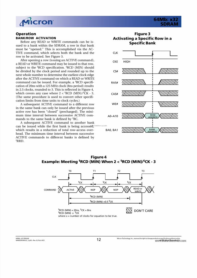
OperationBANK/ROW ACTIVATION
Before any READ or WRITE commands can be is-sued to a bank within the SDRAM, a row in that bank
must be “opened.” This is accomplished via the AC-TIVE command, which selects both the bank and therow to be activated. See Figure 3.
After opening a row (issuing an ACTIVE command),a READ or WRITE command may be issued to that row,subject to the tRCD specification. tRCD (MIN) shouldbe divided by the clock period and rounded up to thenext whole number to determine the earliest clock edgeafter the ACTIVE command on which a READ or WRITEcommand can be issued. For example, a tRCD specifi-cation of 20ns with a 125 MHz clock (8ns period) resultsin 2.5 clocks, rounded to 3. This is reflected in Figure 4, which covers any case where 2 < tRCD (MIN)/tCK - 3.
(The same procedure is used to convert other specifi-cation limits from time units to clock cycles.)
A subsequent ACTIVE command to a different row in the same bank can only be issued after the previousactive row has been “closed” (precharged). The mini-mum time interval between successive ACTIVE com-mands to the same bank is defined by tRC.
A subsequent ACTIVE command to another bank can be issued while the first bank is being accessed, which results in a reduction of total row-access over-head. The minimum time interval between successive ACTIVE commands to different banks is defined by tRRD.
Figure 4Example: Meeting tRCD (MIN) When 2 < tRCD (MIN)/ tCK - 3
CLK
T2T1 T3T0
t
COMMAND NOPACTIVEREAD or
WRITENOP
RCD (MIN)
tRCD (MIN) = 20ns, tCK = 8nstRCD (MIN) x tCKwhere x = number of clocks for equation to be true.
tRCD (MIN) +0.5 tCK
tCK tCK tCK
DON’T CARE
Figure 3Activating a Specific Row in a
Specific Bank
CS#
WE#
CAS#
RAS#
CKE
CLK
A0–A10 ROWADDRESS
HIGH
BA0, BA1 BANKADDRESS
8/11/2019 Mt 48lc2m32b2 - 64mb x32 Sdram
http://slidepdf.com/reader/full/mt-48lc2m32b2-64mb-x32-sdram 13/53
1364Mb: x32 SDRAM Micron Technology, Inc., reserves the right to change products or specifications without notice.
64MSDRAMx32_5.p65 – Rev. B; Pub. 6/02 ©2002, Micron Technology, Inc.
64Mb: x32SDRAM
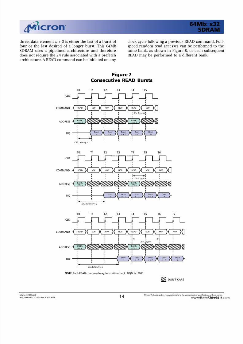
Upon completion of a burst, assuming no other com-mands have been initiated, the DQs will go High-Z. A full-page burst will continue until terminated. (At the
end of the page, it will wrap to column 0 and continue.)Data from any READ burst may be truncated with a
subsequent READ command, and data from a fixed-length READ burst may be immediately followed by data from a READ command. In either case, a continu-ous flow of data can be maintained. The first data ele-ment from the new burst follows either the last ele-ment of a completed burst or the last desired data ele-ment of a longer burst that is being truncated. The new READ command should be issued x cycles before theclock edge at which the last desired data element isvalid, where x equals the CAS latency minus one. Thisis shown in Figure 7 for CAS latencies of one, two and
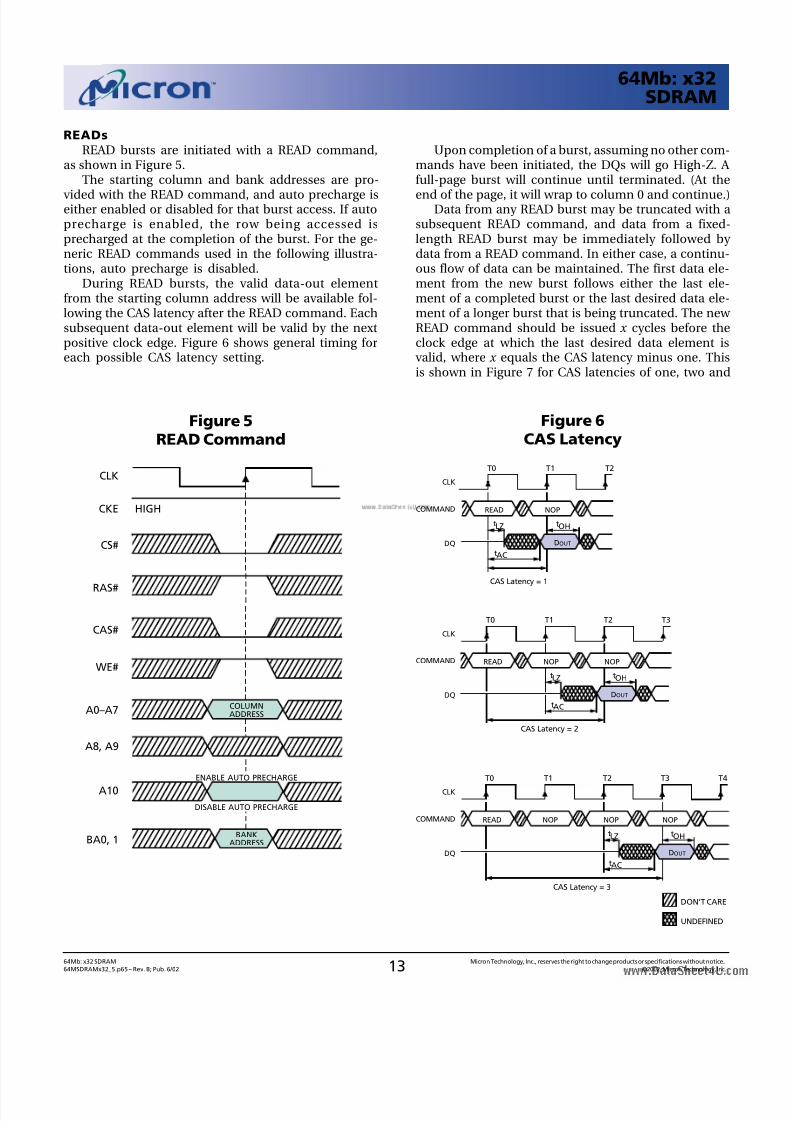
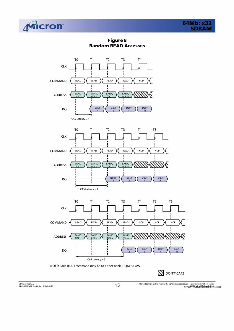
READsREAD bursts are initiated with a READ command,
as shown in Figure 5.The starting column and bank addresses are pro-
vided with the READ command, and auto precharge iseither enabled or disabled for that burst access. If autoprecharge is enabled, the row being accessed isprecharged at the completion of the burst. For the ge-neric READ commands used in the following illustra-tions, auto precharge is disabled.
During READ bursts, the valid data-out elementfrom the starting column address will be available fol-lowing the CAS latency after the READ command. Eachsubsequent data-out element will be valid by the nextpositive clock edge. Figure 6 shows general timing foreach possible CAS latency setting.
Figure 5READ Command
Figure 6CAS Latency
CLK
DQ
T2T1 T3T0
CAS Latency = 3
LZ
DOUT
tOHt
COMMAND NOPREAD
tAC
NOP
T4
NOP
DON’T CARE
UNDEFINED
CLK
DQ
T2T1T0
CAS Latency = 1
LZ
DOUT
tOHt
COMMAND NOPREAD
tAC
CLK
DQ
T2T1 T3T0
CAS Latency = 2
LZ
DOUT
tOHt
COMMAND NOPREAD
tAC
NOP
CS#
WE#
CAS#
RAS#
CKE
CLK
COLUMNADDRESSA0–A7
A10
BA0, 1
HIGH
ENABLE AUTO PRECHARGE
DISABLE AUTO PRECHARGE
BANKADDRESS
A8, A9
8/11/2019 Mt 48lc2m32b2 - 64mb x32 Sdram
http://slidepdf.com/reader/full/mt-48lc2m32b2-64mb-x32-sdram 14/53
1464Mb: x32 SDRAM Micron Technology, Inc., reserves the right to change products or specifications without notice.
64MSDRAMx32_5.p65 – Rev. B; Pub. 6/02 ©2002, Micron Technology, Inc.
64Mb: x32SDRAM
three; data element n + 3 is either the last of a burst of four or the last desired of a longer burst. This 64MbSDRAM uses a pipelined architecture and thereforedoes not require the 2n rule associated with a prefetch
architecture. A READ command can be initiated on any
Figure 7Consecutive READ Bursts
clock cycle following a previous READ command. Full-speed random read accesses can be performed to thesame bank, as shown in Figure 8, or each subsequentREAD may be performed to a different bank.
CLK
DQDOUT
n
T2T1 T4T3 T5T0
COMMAND
ADDRESS
READ NOP NOP NOP
BANK,COL n
NOP
BANK,COL b
DOUT
n + 1DOUT
n + 2DOUT
n + 3DOUT
b
READ
X = 0 cycles
NOTE: Each READ command may be to either bank. DQM is LOW.
CAS Latency = 1
CLK
DQDOUT
n
T2T1 T4T3 T6T5T0
COMMAND
ADDRESS
READ NOP NOP NOP NOP
BANK,COL n
NOP
BANK,COL b
DOUT
n + 1DOUT
n + 2DOUT
n + 3DOUT
b
READ
X = 1 cycle
CAS Latency = 2
CLK
DQDOUT
n
T2T1 T4T3 T6T5T0
COMMAND
ADDRESS
READ NOP NOP NOP NOP
BANK,COL n
NOP
BANK,COL b
DOUT
n + 1DOUT
n + 2DOUT
n + 3DOUT
b
READ NOP
T7
X = 2 cycles
CAS Latency = 3
DON’T CARE
8/11/2019 Mt 48lc2m32b2 - 64mb x32 Sdram
http://slidepdf.com/reader/full/mt-48lc2m32b2-64mb-x32-sdram 15/53
1564Mb: x32 SDRAM Micron Technology, Inc., reserves the right to change products or specifications without notice.
64MSDRAMx32_5.p65 – Rev. B; Pub. 6/02 ©2002, Micron Technology, Inc.
64Mb: x32SDRAM
Figure 8Random READ Accesses
CLK
DQ
T2T1 T4T3 T6T5T0
COMMAND
ADDRESS
READ NOP NOP
BANK,COL n
DON’T CARE
DOUT
n
DOUT
a
DOUT
x
DOUT
m
READ
NOTE: Each READ command may be to either bank. DQM is LOW.
READ READ NOP
BANK,COL a
BANK,COL x
BANK,COL m
CLK
DQDOUT
n
T2T1 T4T3 T5T0
COMMAND
ADDRESS
READ NOP
BANK,COL n
DOUT
a
DOUT
x
DOUT
m
READ READ READ NOP
BANK,COL a
BANK,COL x
BANK,COL m
CLK
DQDOUT
n
T2T1 T4T3T0
COMMAND
ADDRESS
READ NOP
BANK,COL n
DOUT
a
DOUT
x
DOUT
m
READ READ READ
BANK,COL a
BANK,COL x
BANK,COL m
CAS Latency = 1
CAS Latency = 2
CAS Latency = 3
8/11/2019 Mt 48lc2m32b2 - 64mb x32 Sdram
http://slidepdf.com/reader/full/mt-48lc2m32b2-64mb-x32-sdram 16/53
1664Mb: x32 SDRAM Micron Technology, Inc., reserves the right to change products or specifications without notice.
64MSDRAMx32_5.p65 – Rev. B; Pub. 6/02 ©2002, Micron Technology, Inc.
64Mb: x32SDRAM
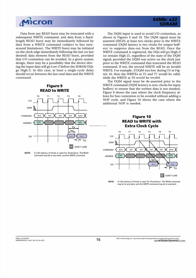
Data from any READ burst may be truncated with asubsequent WRITE command, and data from a fixed-length READ burst may be immediately followed by data from a WRITE command (subject to bus turn-
around limitations). The WRITE burst may be initiatedon the clock edge immediately following the last (or lastdesired) data element from the READ burst, providedthat I/O contention can be avoided. In a given systemdesign, there may be a possibility that the device driv-ing the input data will go Low-Z before the SDRAM DQsgo High-Z. In this case, at least a single-cycle delay should occur between the last read data and the WRITEcommand.
DON’T CARE
READ NOP NOPNOP NOP
DQM
CLK
DQ DOUT n
T2T1 T4T3T0
COMMAND
ADDRESSBANK,COL n
WRITE
DIN b
BANK,COL b
T5
DS
tHZ
t
NOTE: A CAS latency of three is used for illustration. The READ commandmay be to any bank, and the WRITE command may be to any bank.
Figure 10READ to WRITE with
Extra Clock Cycle
Figure 9READ to WRITE
DON’T CARE
READ NOP NOP WRITENOP
CLKT2T1 T4T3T0
DQM
DQ DOUT n
COMMAND
DIN b
ADDRESSBANK,COL n
BANK,COL b
DS
tHZ
t
tCK
NOTE: A CAS latency of three is used for illustration. The READcommand may be to any bank, and the WRITE command
The DQM input is used to avoid I/O contention, asshown in Figures 9 and 10. The DQM signal must beasserted (HIGH) at least two clocks prior to the WRITEcommand (DQM latency is two clocks for output buff-
ers) to suppress data-out from the READ. Once the WRITE command is registered, the DQs will go High-Z(or remain High-Z), regardless of the state of the DQMsignal; provided the DQM was active on the clock justprior to the WRITE command that truncated the READcommand. If not, the second WRITE will be an invalid WRITE. For example, if DQM was low during T4 in Fig-ure 10, then the WRITEs at T5 and T7 would be valid, while the WRITE at T6 would be invalid.
The DQM signal must be de-asserted prior to the WRITE command (DQM latency is zero clocks for inputbuffers) to ensure that the written data is not masked.Figure 9 shows the case where the clock frequency al-
lows for bus contention to be avoided without adding aNOP cycle, and Figure 10 shows the case where theadditional NOP is needed.
8/11/2019 Mt 48lc2m32b2 - 64mb x32 Sdram
http://slidepdf.com/reader/full/mt-48lc2m32b2-64mb-x32-sdram 17/53
1764Mb: x32 SDRAM Micron Technology, Inc., reserves the right to change products or specifications without notice.
64MSDRAMx32_5.p65 – Rev. B; Pub. 6/02 ©2002, Micron Technology, Inc.
64Mb: x32SDRAM
Figure 11READ to PRECHARGE
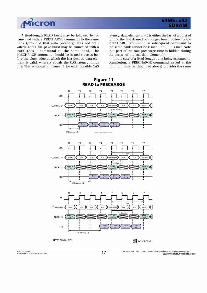
A fixed-length READ burst may be followed by, ortruncated with, a PRECHARGE command to the samebank (provided that auto precharge was not acti-vated), and a full-page burst may be truncated with a
PRECHARGE command to the same bank. ThePRECHARGE command should be issued x cycles be-fore the clock edge at which the last desired data ele-ment is valid, where x equals the CAS latency minusone. This is shown in Figure 11 for each possible CAS
latency; data element n + 3 is either the last of a burst of four or the last desired of a longer burst. Following thePRECHARGE command, a subsequent command tothe same bank cannot be issued until tRP is met. Note
that part of the row precharge time is hidden during the access of the last data element(s).
In the case of a fixed-length burst being executed tocompletion, a PRECHARGE command issued at theoptimum time (as described above) provides the same
CLK
DQDOUT
n
T2T1 T4T3 T6T5T0
COMMAND
ADDRESS
READ NOP NOP NOP NOPNOP
DOUT
n + 1DOUT
n + 2DOUT
n + 3
PRECHARGE ACTIVE
tRP
T7
NOTE: DQM is LOW.
CLK
DQDOUT
n
T2T1 T4T3 T6T5T0
COMMAND
ADDRESS
READ NOP NOP NOP NOPNOP
DOUT
n + 1DOUT
n + 2DOUT
n + 3
PRECHARGE ACTIVE
t RP
T7
CLK
DQDOUT
n
T2T1 T4T3 T6T5T0
COMMAND
ADDRESS
READ NOP NOP NOP NOP
BANK a,COL n
NOP
DOUT
n + 1DOUT
n + 2DOUT
n + 3
PRECHARGE ACTIVE
tRP
T7
BANK a,ROW
BANK(a or all)
DON’T CARE
X = 0 cycles
CAS Latency = 1
X = 1 cycle
CAS Latency = 2
CAS Latency = 3
BANK a,COL n
BANK a,ROW
BANK(a or all)
BANK a,COL n
BANK a,ROW
BANK(a or all)
X = 2 cycles
8/11/2019 Mt 48lc2m32b2 - 64mb x32 Sdram
http://slidepdf.com/reader/full/mt-48lc2m32b2-64mb-x32-sdram 18/53
1864Mb: x32 SDRAM Micron Technology, Inc., reserves the right to change products or specifications without notice.
64MSDRAMx32_5.p65 – Rev. B; Pub. 6/02 ©2002, Micron Technology, Inc.
64Mb: x32SDRAM
Figure 12Terminating a READ Burst
operation that would result from the same fixed-lengthburst with auto precharge. The disadvantage of thePRECHARGE command is that it requires that the com-mand and address buses be available at the appropri-
ate time to issue the command; the advantage of thePRECHARGE command is that it can be used to trun-cate fixed-length or full-page bursts.
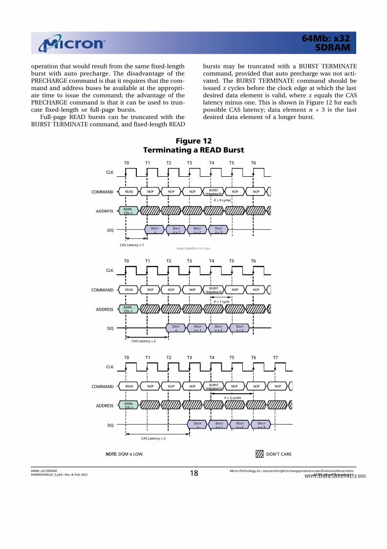
Full-page READ bursts can be truncated with theBURST TERMINATE command, and fixed-length READ
bursts may be truncated with a BURST TERMINATEcommand, provided that auto precharge was not acti-vated. The BURST TERMINATE command should beissued x cycles before the clock edge at which the last
desired data element is valid, where x equals the CASlatency minus one. This is shown in Figure 12 for eachpossible CAS latency; data element n + 3 is the lastdesired data element of a longer burst.
DON’T CARE
CLK
DQDOUT
n
T2T1 T4T3 T6T5T0
COMMAND
ADDRESS
READ NOP NOP NOP NOP
BANK,COL n
NOP
DOUT
n + 1DOUT
n + 2DOUT
n + 3
BURSTTERMINATE
NOP
T7
NOTE: DQM is LOW.
CLK
DQDOUT
n
T2T1 T4T3 T6T5T0
COMMAND
ADDRESS
READ NOP NOP NOP
BANK,COL n
NOP
DOUT
n + 1DOUT
n + 2DOUT
n + 3
BURSTTERMINATE
NOP
CLK
DQDOUT
n
T2T1 T4T3 T6T5T0
COMMAND
ADDRESS
READ NOP NOP NOP
BANK,COL n
NOP
DOUT
n + 1DOUT
n + 2DOUT
n + 3
BURSTTERMINATE NOP
X = 0 cycles
CAS Latency = 1
X = 1 cycle
CAS Latency = 2
CAS Latency = 3
X = 2 cycles
8/11/2019 Mt 48lc2m32b2 - 64mb x32 Sdram
http://slidepdf.com/reader/full/mt-48lc2m32b2-64mb-x32-sdram 19/53
1964Mb: x32 SDRAM Micron Technology, Inc., reserves the right to change products or specifications without notice.
64MSDRAMx32_5.p65 – Rev. B; Pub. 6/02 ©2002, Micron Technology, Inc.
64Mb: x32SDRAM
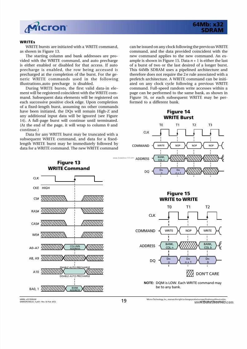
WRITEs WRITE bursts are initiated with a WRITE command,
as shown in Figure 13.The starting column and bank addresses are pro-
vided with the WRITE command, and auto prechargeis either enabled or disabled for that access. If autoprecharge is enabled, the row being accessed isprecharged at the completion of the burst. For the ge-neric WRITE commands used in the following illustrations,auto precharge is disabled.
During WRITE bursts, the first valid data-in ele-ment will be registered coincident with the WRITE com-mand. Subsequent data elements will be registered oneach successive positive clock edge. Upon completionof a fixed-length burst, assuming no other commandshave been initiated, the DQs will remain High-Z andany additional input data will be ignored (see Figure
14). A full-page burst will continue until terminated.(At the end of the page, it will wrap to column 0 andcontinue.)
Data for any WRITE burst may be truncated with asubsequent WRITE command, and data for a fixed-length WRITE burst may be immediately followed by data for a WRITE command. The new WRITE command
Figure 15WRITE to WRITE
can be issued on any clock following the previous WRITEcommand, and the data provided coincident with thenew command applies to the new command. An ex-
ample is shown in Figure 15. Data n + 1 is either the lastof a burst of two or the last desired of a longer burst.This 64Mb SDRAM uses a pipelined architecture andtherefore does not require the 2n rule associated with aprefetch architecture. A WRITE command can be initi-ated on any clock cycle following a previous WRITEcommand. Full-speed random write accesses within apage can be performed to the same bank, as shown inFigure 16, or each subsequent WRITE may be per-formed to a different bank.
CLK
DQDIN
n
T2T1 T3T0
COMMAND
ADDRESS
NOP NOPWRITE
DIN
n + 1
NOP
BANK,COL n
Figure 14WRITE Burst
CS#
WE#
CAS#
RAS#
CKE
CLK
COLUMNADDRESS
HIGH
ENABLE AUTO PRECHARGE
DISABLE AUTO PRECHARGE
BANKADDRESS
A0–A7
A10
BA0, 1
A8, A9
Figure 13WRITE Command
CLK
DQ
T2T1T0
COMMAND
ADDRESS
NOPWRITE WRITE
BANK,COL n
BANK,COL b
DIN
nDIN
n + 1DIN
b
NOTE: DQM is LOW. Each WRITE command maybe to any bank.
DON’T CARE
8/11/2019 Mt 48lc2m32b2 - 64mb x32 Sdram
http://slidepdf.com/reader/full/mt-48lc2m32b2-64mb-x32-sdram 20/53
2064Mb: x32 SDRAM Micron Technology, Inc., reserves the right to change products or specifications without notice.
64MSDRAMx32_5.p65 – Rev. B; Pub. 6/02 ©2002, Micron Technology, Inc.
64Mb: x32SDRAM
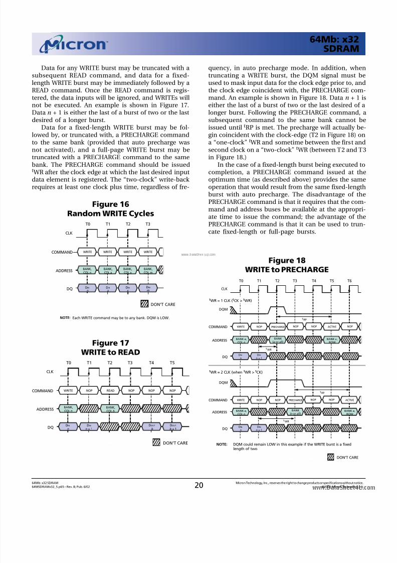
quency, in auto precharge mode. In addition, whentruncating a WRITE burst, the DQM signal must beused to mask input data for the clock edge prior to, andthe clock edge coincident with, the PRECHARGE com-
mand. An example is shown in Figure 18. Data n + 1 iseither the last of a burst of two or the last desired of alonger burst. Following the PRECHARGE command, asubsequent command to the same bank cannot beissued until tRP is met. The precharge will actually be-gin coincident with the clock-edge (T2 in Figure 18) ona “one-clock” t WR and sometime between the first andsecond clock on a “two-clock” t WR (between T2 and T3in Figure 18.)
In the case of a fixed-length burst being executed tocompletion, a PRECHARGE command issued at theoptimum time (as described above) provides the sameoperation that would result from the same fixed-length
burst with auto precharge. The disadvantage of thePRECHARGE command is that it requires that the com-mand and address buses be available at the appropri-ate time to issue the command; the advantage of thePRECHARGE command is that it can be used to trun-cate fixed-length or full-page bursts.
Figure 18WRITE to PRECHARGE
Data for any WRITE burst may be truncated with asubsequent READ command, and data for a fixed-length WRITE burst may be immediately followed by aREAD command. Once the READ command is regis-
tered, the data inputs will be ignored, and WRITEs willnot be executed. An example is shown in Figure 17.Data n + 1 is either the last of a burst of two or the lastdesired of a longer burst.
Data for a fixed-length WRITE burst may be fol-lowed by, or truncated with, a PRECHARGE commandto the same bank (provided that auto precharge wasnot activated), and a full-page WRITE burst may betruncated with a PRECHARGE command to the samebank. The PRECHARGE command should be issuedt WR after the clock edge at which the last desired inputdata element is registered. The “two-clock” write-back requires at least one clock plus time, regardless of fre-
Figure 17WRITE to READ
DON’T CARE
CLK
DQ
T2T1 T3T0
COMMAND
ADDRESS
NOPWRITE
BANK,COL n
DIN
nDIN
n + 1DOUT
b
READ NOP NOP
BANK,COL b
NOP
DOUT
b + 1
T4 T5
Figure 16Random WRITE Cycles
DON’T CARE
CLK
DQ DIN
n
T2T1 T3T0
COMMAND
ADDRESS
WRITE
BANK,COL n
DIN
a
DIN
x
DIN
m
WRITE WRITE WRITE
BANK,COL a
BANK,COL x
BANK,COL m
NOTE: Each WRITE command may be to any bank. DQM is LOW.
DON’T CARE
DQM
CLK
DQ
T2T1 T4T3T0
COMMAND
ADDRESS BANK a,COL n
T5
NOPWRITE PRECHARGE NOPNOP
DIN
nDIN
n + 1
ACTIVE
tRP
BANK(a or all)
t WR
BANK a,ROW
DQM
DQ
COMMAND
ADDRESS BANK a,COL n
NOPWRITE PRECHARGE NOPNOP
DIN
n
DIN
n + 1
ACTIVE
tRP
BANK(a or all)
t WR
NOTE: DQM could remain LOW in this example if the WRITE burst is a fixedlength of two.
BANK a,ROW
T6
NOP
NOP
tWR = 2 CLK (when tWR > tCK)
tWR = 1 CLK (tCK > tWR)
8/11/2019 Mt 48lc2m32b2 - 64mb x32 Sdram
http://slidepdf.com/reader/full/mt-48lc2m32b2-64mb-x32-sdram 21/53
2164Mb: x32 SDRAM Micron Technology, Inc., reserves the right to change products or specifications without notice.
64MSDRAMx32_5.p65 – Rev. B; Pub. 6/02 ©2002, Micron Technology, Inc.
64Mb: x32SDRAM
Fixed-length or full-page WRITE bursts can be trun-cated with the BURST TERMINATE command. Whentruncating a WRITE burst, the input data applied coin-cident with the BURST TERMINATE command will be
ignored. The last data written (provided that DQM isLOW at that time) will be the input data applied oneclock previous to the BURST TERMINATE command.This is shown in Figure 19, where data n is the lastdesired data element of a longer burst.
Figure 21Power-Down
DON’T CARE
tRAS
tRCD
tRC
All banks idleInput buffers gated off
Exit power-down mode.
()()
()()
()()
tCKS > tCKS
COMMAND NOP ACTIVE
Enter power-down mode.
NOP
CLK
CKE
()()
()()
Figure 20PRECHARGE Command
Figure 19Terminating a WRITE Burst
CLK
DQ
T2T1T0
COMMAND
ADDRESSBANK,COL n
WRITEBURST
TERMINATENEXT
COMMAND
DIN
n
(ADDRESS)
(DATA)
NOTE: DQMs are LOW.
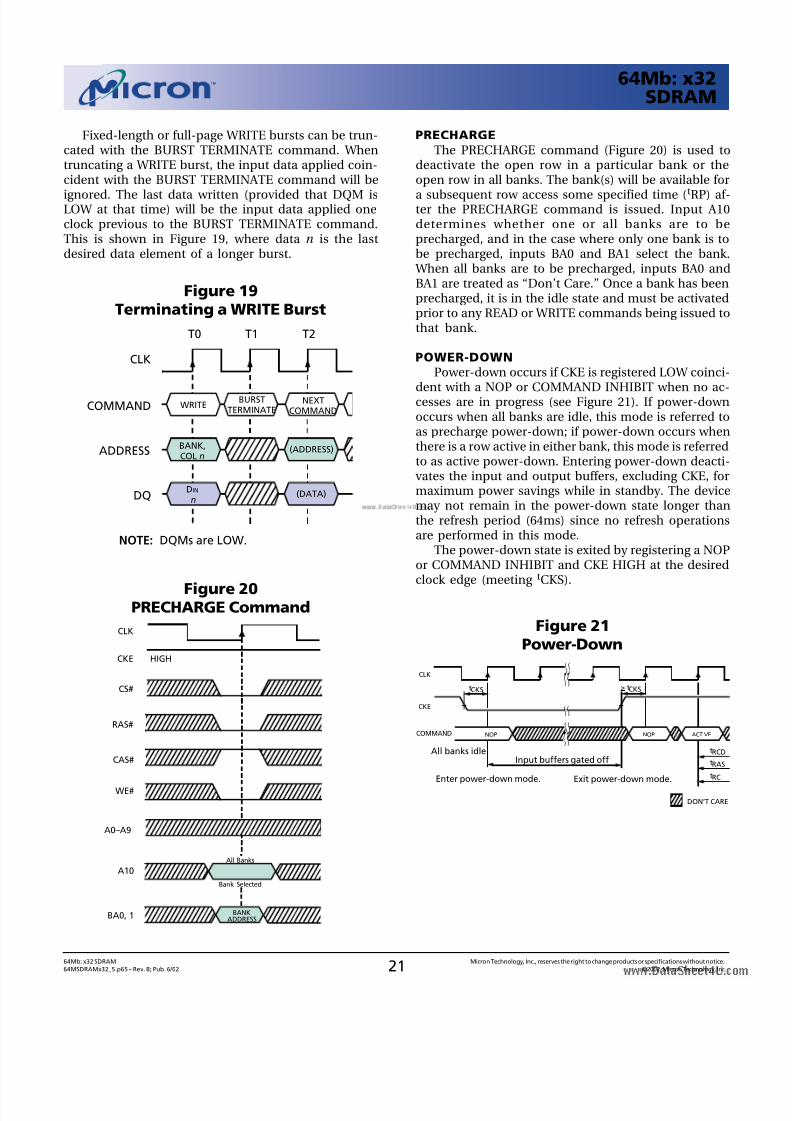
PRECHARGEThe PRECHARGE command (Figure 20) is used to
deactivate the open row in a particular bank or theopen row in all banks. The bank(s) will be available for
a subsequent row access some specified time (tRP) af-ter the PRECHARGE command is issued. Input A10determines whether one or all banks are to beprecharged, and in the case where only one bank is tobe precharged, inputs BA0 and BA1 select the bank. When all banks are to be precharged, inputs BA0 andBA1 are treated as “Don’t Care.” Once a bank has beenprecharged, it is in the idle state and must be activatedprior to any READ or WRITE commands being issued tothat bank.
POWER-DOWNPower-down occurs if CKE is registered LOW coinci-
dent with a NOP or COMMAND INHIBIT when no ac-cesses are in progress (see Figure 21). If power-downoccurs when all banks are idle, this mode is referred toas precharge power-down; if power-down occurs whenthere is a row active in either bank, this mode is referredto as active power-down. Entering power-down deacti-vates the input and output buffers, excluding CKE, formaximum power savings while in standby. The devicemay not remain in the power-down state longer thanthe refresh period (64ms) since no refresh operationsare performed in this mode.
The power-down state is exited by registering a NOPor COMMAND INHIBIT and CKE HIGH at the desiredclock edge (meeting tCKS).
CS#
WE#
CAS#
RAS#
CKE
CLK
A10
HIGH
All Banks
Bank Selected
A0–A9
BA0, 1 BANKADDRESS
8/11/2019 Mt 48lc2m32b2 - 64mb x32 Sdram
http://slidepdf.com/reader/full/mt-48lc2m32b2-64mb-x32-sdram 22/53
2264Mb: x32 SDRAM Micron Technology, Inc., reserves the right to change products or specifications without notice.
64MSDRAMx32_5.p65 – Rev. B; Pub. 6/02 ©2002, Micron Technology, Inc.
64Mb: x32SDRAM
DON’T CARE
DIN
COMMAND
ADDRESS
WRITE
BANK,COL n
DIN
n
NOPNOP
CLK
T2T1 T4T3 T5T0
CKE
INTERNALCLOCK
NOP
DIN
n + 1DIN
n + 2
Figure 22CLOCK SUSPEND During WRITE Burst
DON’T CARE
CLK
DQDOUT
n
T2T1 T4T3 T6T5T0
COMMAND
ADDRESS
READ NOP NOP NOP
BANK,COL n
NOP
DOUT
n + 1DOUT
n + 2DOUT
n + 3
NOTE: For this example, CAS latency = 2, burst length = 4 or greater, andDQM is LOW.
CKE
INTERNALCLOCK
NOP
Figure 23CLOCK SUSPEND During READ Burst
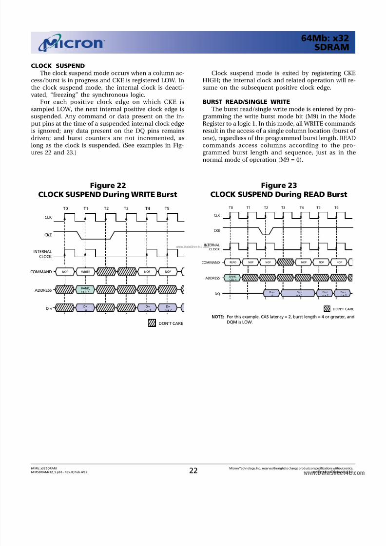
CLOCK SUSPENDThe clock suspend mode occurs when a column ac-
cess/burst is in progress and CKE is registered LOW. Inthe clock suspend mode, the internal clock is deacti-
vated, “freezing” the synchronous logic.For each positive clock edge on which CKE is
sampled LOW, the next internal positive clock edge issuspended. Any command or data present on the in-put pins at the time of a suspended internal clock edgeis ignored; any data present on the DQ pins remainsdriven; and burst counters are not incremented, aslong as the clock is suspended. (See examples in Fig-ures 22 and 23.)
Clock suspend mode is exited by registering CKEHIGH; the internal clock and related operation will re-sume on the subsequent positive clock edge.
BURST READ/SINGLE WRITEThe burst read/single write mode is entered by pro-
gramming the write burst mode bit (M9) in the ModeRegister to a logic 1. In this mode, all WRITE commandsresult in the access of a single column location (burst of one), regardless of the programmed burst length. READcommands access columns according to the pro-grammed burst length and sequence, just as in thenormal mode of operation (M9 = 0).
8/11/2019 Mt 48lc2m32b2 - 64mb x32 Sdram
http://slidepdf.com/reader/full/mt-48lc2m32b2-64mb-x32-sdram 23/53
2364Mb: x32 SDRAM Micron Technology, Inc., reserves the right to change products or specifications without notice.
64MSDRAMx32_5.p65 – Rev. B; Pub. 6/02 ©2002, Micron Technology, Inc.
64Mb: x32SDRAM
CONCURRENT AUTO PRECHARGE An access command to (READ or WRITE) another
bank while an access command with auto prechargeenabled is executing is not allowed by SDRAMs, unless
the SDRAM supports CONCURRENT AUTOPRECHARGE. Micron SDRAMs support CONCURRENT AUTO PRECHARGE. Four cases where CONCURRENT AUTO PRECHARGE occurs are defined below.
READ with auto precharge1. Interrupted by a READ (with or without auto
precharge): A READ to bank m will interrupt a READ
on bank n, CAS latency later. The PRECHARGE tobank n will begin when the READ to bank m is regis-tered (Figure 24).
2. Interrupted by a WRITE (with or without autoprecharge): A WRITE to bank m will interrupt a READon bank n when registered. DQM should be usedtwo clocks prior to the WRITE command to preventbus contention. The PRECHARGE to bank n willbegin when the WRITE to bank m is registered (Fig-ure 25).
CLK
DQDOUT
a
T2T1 T4T3 T6T5T0
COMMANDREAD - AP
BANK nNOP NOPNOPNOP
DOUT
a + 1DOUT
d
DOUT
d + 1
NOP
T7
BANK n
CAS Latency = 3 (BANK m)
BANK m
ADDRESS
Idle
NOP
NOTE: D M i s LOW.
BANK n,COL a
BANK m,COL d
READ - APBANK m
Internal
States
t
Page Act ive READ with Bur st of 4 Inter rupt Bur st , Precharge
Page Active READ with Burst of 4 Precharge
RP - BANK n tRP - BANK m
CAS Latency = 3 (BANK n)
Figure 24READ With Auto Precharge Interrupted by a READ
CLK
DQDOUT
a
T2T1 T4T3 T6T5T0
COMMAND NOPNOPNOPNOP
DIN
d + 1DIN
d
DIN
d + 2DIN
d + 3
NOP
T7
BANK n
BANKm
ADDRESS
Idle
NOP
DQM
NOTE: 1. DQM is HIGH at T2 to prevent DOUT-a+1 from contending with DIN-d at T4.
BANK n,COL a
BANK m,COL d
WRITE - APBANKm
Internal
States
t
PageActive
READ with Burst of 4 Interrupt Burst, Precharge
Page Active WRITE with Burst of 4 Write-Back
RP - BANK n t WR - BANK m
CAS Latency = 3 (BANK n)
READ - APBANK n
1
DON’T CARE
Figure 25READ With Auto Precharge Interrupted by a WRITE
8/11/2019 Mt 48lc2m32b2 - 64mb x32 Sdram
http://slidepdf.com/reader/full/mt-48lc2m32b2-64mb-x32-sdram 24/53
2464Mb: x32 SDRAM Micron Technology, Inc., reserves the right to change products or specifications without notice.
64MSDRAMx32_5.p65 – Rev. B; Pub. 6/02 ©2002, Micron Technology, Inc.
64Mb: x32SDRAM
CLK
DQ
T2T1 T4T3 T6T5T0
COMMAND WRITE - APBANK n
NOPNOPNOPNOP
DIN
a + 1DIN
a
NOP NOP
T7
BANK n
BANK m
ADDRESS
NOTE: 1. DQM is LOW.
BANK n,COL a
BANK m,COL d
READ - APBANKm
Internal
States
t
Page Active WRITE with Burst of 4 Interrupt Burst, Wri te-Back Precharge
Page Active READ with Burst of 4
t
tRP - BANK m
DOUT
d
DOUT
d + 1
CAS Latency = 3 (BANK m)
RP - BANK nWR - BANK n
Figure 26WRITE With Auto Precharge Interrupted by a READ
DON’T CARE
CLK
DQ
T2T1 T4T3 T6T5T0
COMMANDWRITE - AP
BANK nNOPNOPNOPNOP
DIN
d + 1DIN
d
DIN
a + 1DIN
a + 2DIN
a
DIN
d + 2DIN
d + 3
NOP
T7
BANK n
BANK m
ADDRESS
NOP
NOTE: 1. DQM is LOW.
BANK n,COL a
BANK m,COL d
WRITE - APBANK m
Internal
States
t
Page Active WRITE with Burst of 4 Interrupt Burst, Write-Back Precharge
Page Active WRITE with Burst of 4 Write-Back
WR - BANK ntRP - BANK n
t WR - BANK m
Figure 27WRITE With Auto Precharge Interrupted by a WRITE
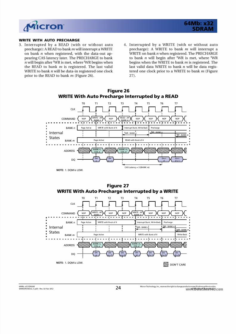
WRITE WITH AUTO PRECHARGE3. Interrupted by a READ (with or without auto
precharge): A READ to bank m will interrupt a WRITEon bank n when registered, with the data-out ap-
pearing CAS latency later. The PRECHARGE to bank n will begin after t WR is met, where t WR begins whenthe READ to bank m is registered. The last valid WRITE to bank n will be data-in registered one clock prior to the READ to bank m (Figure 26).
4. Interrupted by a WRITE (with or without autoprecharge): A WRITE to bank m will interrupt a WRITE on bank n when registered. The PRECHARGE
to bank n will begin after t WR is met, where t WRbegins when the WRITE to bank m is registered. Thelast valid data WRITE to bank n will be data regis-tered one clock prior to a WRITE to bank m (Figure27).
8/11/2019 Mt 48lc2m32b2 - 64mb x32 Sdram
http://slidepdf.com/reader/full/mt-48lc2m32b2-64mb-x32-sdram 25/53
2564Mb: x32 SDRAM Micron Technology, Inc., reserves the right to change products or specifications without notice.
64MSDRAMx32_5.p65 – Rev. B; Pub. 6/02 ©2002, Micron Technology, Inc.
64Mb: x32SDRAM
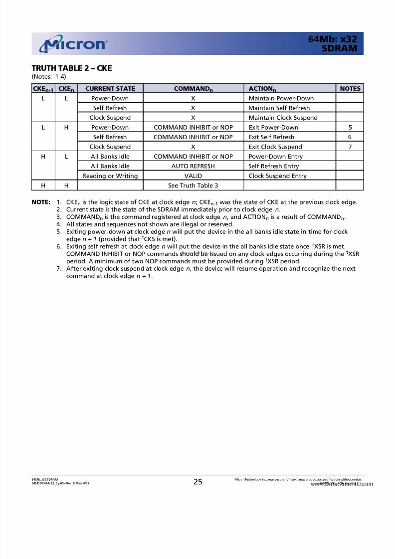
TRUTH TABLE 2 – CKE(Notes: 1-4)
CKEn-1 CKEn CURRENT STATE COMMANDn ACTIONn NOTES
L L Power-Down X Maintain Power-DownSelf Refresh X Maintain Self Refresh
Clock Suspend X Maintain Clock Suspend
L H Power-Down COMMAND INHIBIT or NOP Exit Power-Down 5
Self Refresh COMMAND INHIBIT or NOP Exit Self Refresh 6
Clock Suspend X Exit Clock Suspend 7
H L All Banks Idle COMMAND INHIBIT or NOP Power-Down Entry
All Banks Idle AUTO REFRESH Self Refresh Entry
Reading or Writing VALID Clock Suspend Entry
H H See Truth Table 3
NOTE: 1. CKEn is the logic state of CKE at clock edge n; CKEn-1 was the state of CKE at the previous clock edge.2. Current state is the state of the SDRAM immediately prior to clock edge n.3. COMMANDn is the command registered at clock edge n, and ACTIONn is a result of COMMANDn.4. All states and sequences not shown are illegal or reserved.5. Exiting power-down at clock edge n will put the device in the all banks idle state in time for clock
edge n + 1 (provided that tCKS is met).6. Exiting self refresh at clock edge n will put the device in the all banks idle state once tXSR is met.
COMMAND INHIBIT or NOP commands should be issued on any clock edges occurring during the tXSRperiod. A minimum of two NOP commands must be provided during tXSR period.
7. After exiting clock suspend at clock edge n, the device will resume operation and recognize the nextcommand at clock edge n + 1.
8/11/2019 Mt 48lc2m32b2 - 64mb x32 Sdram
http://slidepdf.com/reader/full/mt-48lc2m32b2-64mb-x32-sdram 26/53
2664Mb: x32 SDRAM Micron Technology, Inc., reserves the right to change products or specifications without notice.
64MSDRAMx32_5.p65 – Rev. B; Pub. 6/02 ©2002, Micron Technology, Inc.
64Mb: x32SDRAM
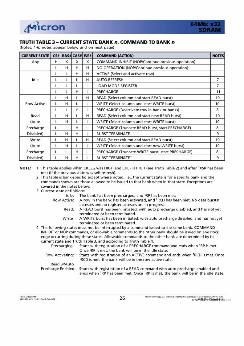
TRUTH TABLE 3 – CURRENT STATE BANK n, COMMAND TO BANK n(Notes: 1-6; notes appear below and on next page)
CURRENT STATE CS# RAS# CAS# WE# COMMAND (ACTION) NOTES
Any H X X X COMMAND INHIBIT (NOP/Continue previous operation)
L H H H NO OPERATION (NOP/Continue previous operation)
L L H H ACTIVE (Select and activate row)
Idle L L L H AUTO REFRESH 7
L L L L LOAD MODE REGISTER 7
L L H L PRECHARGE 11
L H L H READ (Select column and start READ burst) 10
Row Active L H L L WRITE (Select column and start WRITE burst) 10
L L H L PRECHARGE (Deactivate row in bank or banks) 8
Read L H L H READ (Select column and start new READ burst) 10
(Auto L H L L WRITE (Select column and start WRITE burst) 10
Precharge L L H L PRECHARGE (Truncate READ burst, start PRECHARGE) 8
Disabled) L H H L BURST TERMINATE 9
Write L H L H READ (Select column and start READ burst) 10
(Auto L H L L WRITE (Select column and start new WRITE burst) 10
Precharge L L H L PRECHARGE (Truncate WRITE burst, start PRECHARGE) 8
Disabled) L H H L BURST TERMINATE 9
NOTE: 1. This table applies when CKEn-1 was HIGH and CKEn is HIGH (see Truth Table 2) and after tXSR has beenmet (if the previous state was self refresh).
2. This table is bank-specific, except where noted, i.e., the current state is for a specific bank and the
commands shown are those allowed to be issued to that bank when in that state. Exceptions arecovered in the notes below.
3. Current state definitions:Idle: The bank has been precharged, and tRP has been met.
Row Active: A row in the bank has been activated, and tRCD has been met. No data bursts/ accesses and no register accesses are in progress.
Read: A READ burst has been initiated, with auto precharge disabled, and has not yetterminated or been terminated.
Write: A WRITE burst has been initiated, with auto precharge disabled, and has not yetterminated or been terminated.
4. The following states must not be interrupted by a command issued to the same bank. COMMANDINHIBIT or NOP commands, or allowable commands to the other bank should be issued on any clockedge occurring during these states. Allowable commands to the other bank are determined by its
current state and Truth Table 3, and according to Truth Table 4.Precharging: Starts with registration of a PRECHARGE command and ends when tRP is met.Once tRP is met, the bank will be in the idle state.
Row Activating: Starts with registration of an ACTIVE command and ends when tRCD is met. OncetRCD is met, the bank will be in the row active state.
Read w/AutoPrecharge Enabled: Starts with registration of a READ command with auto precharge enabled and
ends when tRP has been met. Once tRP is met, the bank will be in the idle state.
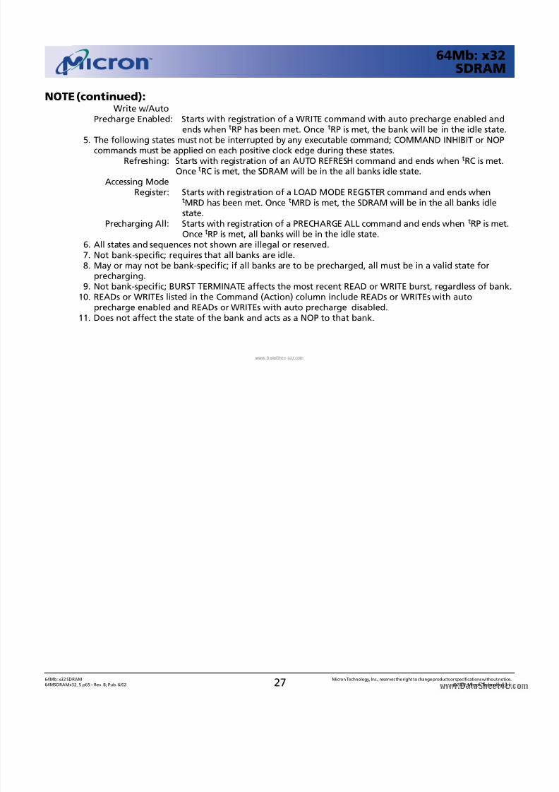
8/11/2019 Mt 48lc2m32b2 - 64mb x32 Sdram
http://slidepdf.com/reader/full/mt-48lc2m32b2-64mb-x32-sdram 27/53
8/11/2019 Mt 48lc2m32b2 - 64mb x32 Sdram
http://slidepdf.com/reader/full/mt-48lc2m32b2-64mb-x32-sdram 28/53
2864Mb: x32 SDRAM Micron Technology, Inc., reserves the right to change products or specifications without notice.
64MSDRAMx32_5.p65 – Rev. B; Pub. 6/02 ©2002, Micron Technology, Inc.
64Mb: x32SDRAM
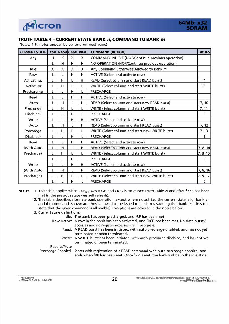
TRUTH TABLE 4 – CURRENT STATE BANK n, COMMAND TO BANKm(Notes: 1-6; notes appear below and on next page)
CURRENT STATE CS# RAS# CAS# WE# COMMAND (ACTION) NOTES
Any H X X X COMMAND INHIBIT (NOP/Continue previous operation)
L H H H NO OPERATION (NOP/Continue previous operation)
Idle X X X X Any Command Otherwise Allowed to Bank m
Row L L H H ACTIVE (Select and activate row)
Activating, L H L H READ (Select column and start READ burst) 7
Active, or L H L L WRITE (Select column and start WRITE burst) 7
Precharging L L H L PRECHARGE
Read L L H H ACTIVE (Select and activate row)
(Auto L H L H READ (Select column and start new READ burst) 7, 10
Precharge L H L L WRITE (Select column and start WRITE burst) 7, 11
Disabled) L L H L PRECHARGE 9
Write L L H H ACTIVE (Select and activate row)
(Auto L H L H READ (Select column and start READ burst) 7, 12
Precharge L H L L WRITE (Select column and start new WRITE burst) 7, 13
Disabled) L L H L PRECHARGE 9
Read L L H H ACTIVE (Select and activate row)
(With Auto L H L H READ (Select column and start new READ burst) 7, 8, 14
Precharge) L H L L WRITE (Select column and start WRITE burst) 7, 8, 15
L L H L PRECHARGE 9
Write L L H H ACTIVE (Select and activate row)
(With Auto L H L H READ (Select column and start READ burst) 7, 8, 16Precharge) L H L L WRITE (Select column and start new WRITE burst) 7, 8, 17
L L H L PRECHARGE 9
NOTE: 1. This table applies when CKEn-1 was HIGH and CKEn is HIGH (see Truth Table 2) and after tXSR has beenmet (if the previous state was self refresh).
2. This table describes alternate bank operation, except where noted; i.e., the current state is for bank nand the commands shown are those allowed to be issued to bank m (assuming that bank m is in such astate that the given command is allowable). Exceptions are covered in the notes below.
3. Current state definitions:Idle: The bank has been precharged, and tRP has been met.
Row Active: A row in the bank has been activated, and tRCD has been met. No data bursts/
accesses and no register accesses are in progress.Read: A READ burst has been initiated, with auto precharge disabled, and has not yetterminated or been terminated.
Write: A WRITE burst has been initiated, with auto precharge disabled, and has not yetterminated or been terminated.
Read w/AutoPrecharge Enabled: Starts with registration of a READ command with auto precharge enabled, and
ends when tRP has been met. Once tRP is met, the bank will be in the idle state.
8/11/2019 Mt 48lc2m32b2 - 64mb x32 Sdram
http://slidepdf.com/reader/full/mt-48lc2m32b2-64mb-x32-sdram 29/53
2964Mb: x32 SDRAM Micron Technology, Inc., reserves the right to change products or specifications without notice.
64MSDRAMx32_5.p65 – Rev. B; Pub. 6/02 ©2002, Micron Technology, Inc.
64Mb: x32SDRAM
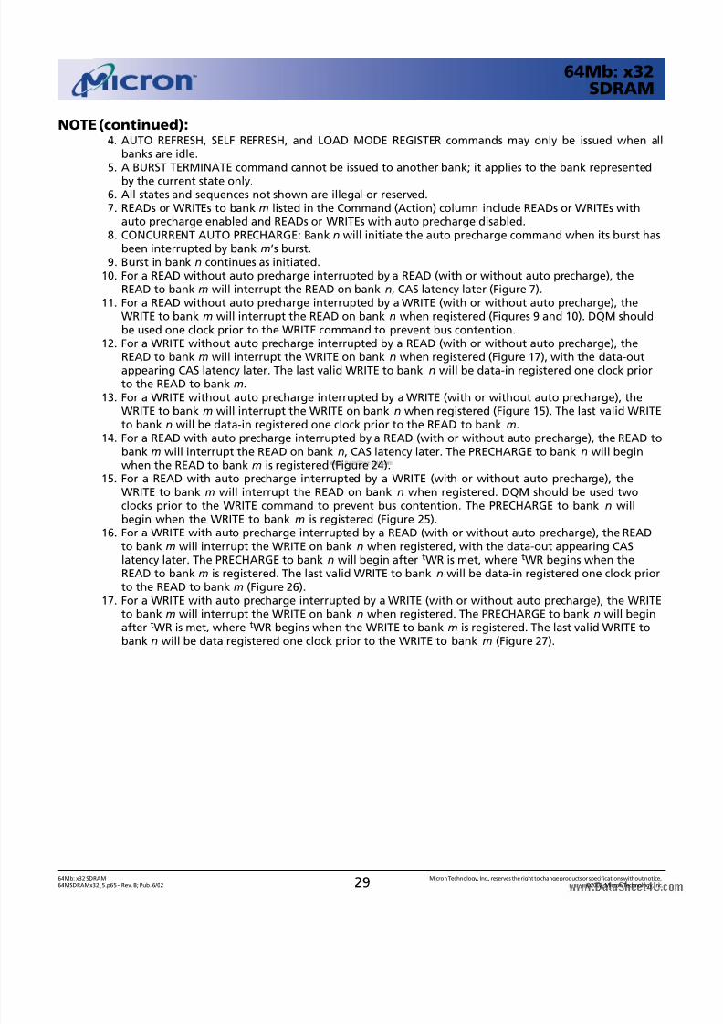
NOTE (continued):4. AUTO REFRESH, SELF REFRESH, and LOAD MODE REGISTER commands may only be issued when all
banks are idle.5. A BURST TERMINATE command cannot be issued to another bank; it applies to the bank represented
by the current state only.6. All states and sequences not shown are illegal or reserved.7. READs or WRITEs to bank m listed in the Command (Action) column include READs or WRITEs with
auto precharge enabled and READs or WRITEs with auto precharge disabled.8. CONCURRENT AUTO PRECHARGE: Bank n will initiate the auto precharge command when its burst has
been interrupted by bank m’s burst.9. Burst in bank n continues as initiated.
10. For a READ without auto precharge interrupted by a READ (with or without auto precharge), theREAD to bank m will interrupt the READ on bank n, CAS latency later (Figure 7).
11. For a READ without auto precharge interrupted by a WRITE (with or without auto precharge), theWRITE to bank m will interrupt the READ on bank n when registered (Figures 9 and 10). DQM shouldbe used one clock prior to the WRITE command to prevent bus contention.
12. For a WRITE without auto precharge interrupted by a READ (with or without auto precharge), the
READ to bank m will interrupt the WRITE on bank n when registered (Figure 17), with the data-outappearing CAS latency later. The last valid WRITE to bank n will be data-in registered one clock priorto the READ to bank m.
13. For a WRITE without auto precharge interrupted by a WRITE (with or without auto precharge), theWRITE to bank m will interrupt the WRITE on bank n when registered (Figure 15). The last valid WRITEto bank n will be data-in registered one clock prior to the READ to bank m.
14. For a READ with auto precharge interrupted by a READ (with or without auto precharge), the READ tobank m will interrupt the READ on bank n, CAS latency later. The PRECHARGE to bank n will beginwhen the READ to bank m is registered (Figure 24).
15. For a READ with auto precharge interrupted by a WRITE (with or without auto precharge), theWRITE to bank m will interrupt the READ on bank n when registered. DQM should be used twoclocks prior to the WRITE command to prevent bus contention. The PRECHARGE to bank n willbegin when the WRITE to bank m is registered (Figure 25).
16. For a WRITE with auto precharge interrupted by a READ (with or without auto precharge), the READto bank m will interrupt the WRITE on bank n when registered, with the data-out appearing CASlatency later. The PRECHARGE to bank n will begin after tWR is met, where tWR begins when theREAD to bank m is registered. The last valid WRITE to bank n will be data-in registered one clock priorto the READ to bank m (Figure 26).
17. For a WRITE with auto precharge interrupted by a WRITE (with or without auto precharge), the WRITEto bank m will interrupt the WRITE on bank n when registered. The PRECHARGE to bank n will beginafter tWR is met, where tWR begins when the WRITE to bank m is registered. The last valid WRITE tobank n will be data registered one clock prior to the WRITE to bank m (Figure 27).
8/11/2019 Mt 48lc2m32b2 - 64mb x32 Sdram
http://slidepdf.com/reader/full/mt-48lc2m32b2-64mb-x32-sdram 30/53
3064Mb: x32 SDRAM Micron Technology, Inc., reserves the right to change products or specifications without notice.
64MSDRAMx32_5.p65 – Rev. B; Pub. 6/02 ©2002, Micron Technology, Inc.
64Mb: x32SDRAM
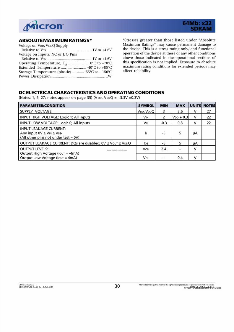
ABSOLUTE MAXIMUM RATINGS* Voltage on V DD, V DDQ Supply
Relative to V SS .............................................. -1V to +4.6V Voltage on Inputs, NC or I/O Pins
Relative to V SS .............................................. -1V to +4.6V Operating Temperature, T A ............................ 0°C to +70°CExtended Temperature .......................... -40°C to +85°CStorage Temperature (plastic) ............ -55°C to +150°CPower Dissipation ........................................................ 1W
*Stresses greater than those listed under “AbsoluteMaximum Ratings” may cause permanent damage tothe device. This is a stress rating only, and functionaloperation of the device at these or any other conditions
above those indicated in the operational sections of this specification is not implied. Exposure to absolutemaximum rating conditions for extended periods may affect reliability.
DC ELECTRICAL CHARACTERISTICS AND OPERATING CONDITIONS(Notes: 1, 6, 27; notes appear on page 35) (VDD, VDDQ = +3.3V ±0.3V)
PARAMETER/CONDITION SYMBOL MIN MAX UNITS NOTES
SUPPLY VOLTAGE VDD, VDDQ 3 3.6 V 27
INPUT HIGH VOLTAGE: Logic 1; All inputs VIH 2 VDD + 0.3 V 22
INPUT LOW VOLTAGE: Logic 0; All inputs VIL -0.3 0.8 V 22
INPUT LEAKAGE CURRENT:Any input 0V ≤ VIN ≤ VDD II -5 5 µA(All other pins not under test = 0V)
OUTPUT LEAKAGE CURRENT: DQs are disabled; 0V ≤ VOUT ≤ VDDQ IOZ -5 5 µA
OUTPUT LEVELS: VOH 2.4 – VOutput High Voltage (IOUT = -4mA)Output Low Voltage (IOUT = 4mA) VOL – 0.4 V
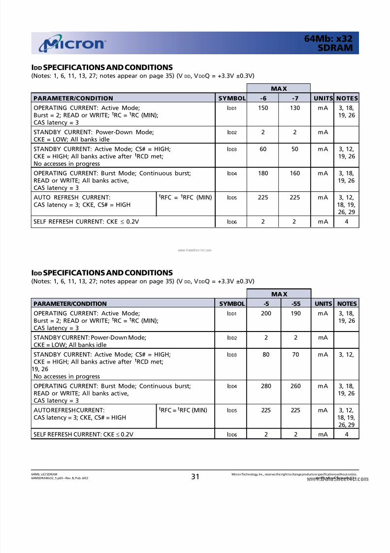
8/11/2019 Mt 48lc2m32b2 - 64mb x32 Sdram
http://slidepdf.com/reader/full/mt-48lc2m32b2-64mb-x32-sdram 31/53
3164Mb: x32 SDRAM Micron Technology, Inc., reserves the right to change products or specifications without notice.
64MSDRAMx32_5.p65 – Rev. B; Pub. 6/02 ©2002, Micron Technology, Inc.
64Mb: x32SDRAM
IDD SPECIFICATIONS AND CONDITIONS(Notes: 1, 6, 11, 13, 27; notes appear on page 35) (V DD, VDDQ = +3.3V ±0.3V)
PARAMETER/CONDITION SYMBOL -5 -55 UNITS NOTES
OPERATING CURRENT: Active Mode; IDD1 200 190 mA 3, 18,Burst = 2; READ or WRITE; tRC = tRC (MIN); 19, 26CAS latency = 3
STANDBY CURRENT: Power-Down Mode; IDD2 2 2 mACKE = LOW; All banks idle
STANDBY CURRENT: Active Mode; CS# = HIGH; IDD3 80 70 mA 3, 12,CKE = HIGH; All banks active after tRCD met;
19, 26No accesses in progress
OPERATING CURRENT: Burst Mode; Continuous burst; IDD4 280 260 mA 3, 18,READ or WRITE; All banks active, 19, 26CAS latency = 3
AUTO REFRESH CURRENT: tRFC = tRFC (MIN) IDD5 225 225 mA 3, 12,CAS latency = 3; CKE, CS# = HIGH 18, 19,
26, 29
SELF REFRESH CURRENT: CKE ≤ 0.2V IDD6 2 2 mA 4
MAX
IDD SPECIFICATIONS AND CONDITIONS(Notes: 1, 6, 11, 13, 27; notes appear on page 35) (V DD, VDDQ = +3.3V ±0.3V)
PARAMETER/CONDITION SYMBOL -6 -7 UNITS NOTES
OPERATING CURRENT: Active Mode; IDD1 150 130 mA 3, 18,Burst = 2; READ or WRITE; tRC = tRC (MIN); 19, 26CAS latency = 3
STANDBY CURRENT: Power-Down Mode; IDD2 2 2 mACKE = LOW; All banks idle
STANDBY CURRENT: Active Mode; CS# = HIGH; IDD3 60 50 mA 3, 12,CKE = HIGH; All banks active after tRCD met; 19, 26No accesses in progress
OPERATING CURRENT: Burst Mode; Continuous burst; IDD4 180 160 mA 3, 18,READ or WRITE; All banks active, 19, 26CAS latency = 3
AUTO REFRESH CURRENT: tRFC = tRFC (MIN) IDD5 225 225 mA 3, 12,CAS latency = 3; CKE, CS# = HIGH 18, 19,
26, 29
SELF REFRESH CURRENT: CKE ≤ 0.2V IDD6 2 2 mA 4
MAX
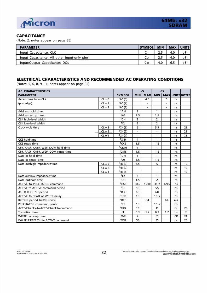
8/11/2019 Mt 48lc2m32b2 - 64mb x32 Sdram
http://slidepdf.com/reader/full/mt-48lc2m32b2-64mb-x32-sdram 32/53
3264Mb: x32 SDRAM Micron Technology, Inc., reserves the right to change products or specifications without notice.
64MSDRAMx32_5.p65 – Rev. B; Pub. 6/02 ©2002, Micron Technology, Inc.
64Mb: x32SDRAM
ELECTRICAL CHARACTERISTICS AND RECOMMENDED AC OPERATING CONDITIONS(Notes: 5, 6, 8, 9, 11; notes appear on page 35)
AC CHARACTERISTICS -5 -55
PARAMETER SYMBOL MIN MAX MIN MAX UNITS NOTES
Access time from CLK CL = 3 tAC (3) 4.5 5 ns
(pos. edge) CL = 2 tAC (2) - - nsCL = 1 tAC (1) - - ns
Address hold time tAH 1 1 ns
Address setup time tAS 1.5 1.5 ns
CLK high-level width tCH 2 2 ns
CLK low-level width tCL 2 2 ns
Clock cycle time CL = 3 tCK (3) 5 5.5 ns 23
CL = 2 tCK (2) - - ns 23
CL = 1 tCK (1) - - ns 23
CKE hold time tCKH 1 1 ns
CKE setup time tCKS 1.5 1.5 ns
CS#, RAS#, CAS#, WE#, DQM hold time tCMH 1 1 ns
CS#, RAS#, CAS#, WE#, DQM setup time tCMS 1.5 1.5 ns
Data-in hold time tDH 1 1 ns
Data-in setup time tDS 1.5 1.5 ns
Data-out high-impedance time CL = 3 tHZ (3) 4.5 5 ns 10
CL = 2 tHZ (2) - - ns 10
CL = 1 tHZ (1) - - ns 10
Data-out low-impedance time tLZ 1 1 ns
Data-out hold time tOH 1.5 2 ns
ACTIVE to PRECHARGE command tRAS 38.7 120k 38.7 120k ns
ACTIVE to ACTIVE command period tRC 55 55 ns
AUTO REFRESH period tRFC 60 60 ns
ACTIVE to READ or WRITE delay tRCD 15 16.5 ns
Refresh period (4,096 rows) tREF 64 64 ms
PRECHARGE command periodt
RP 15 16.5 nsACTIVE banka to ACTIVE bankb command tRRD 10 11 ns 25
Transition time tT 0.3 1.2 0.3 1.2 ns 7
WRITE recovery time tWR 2 2 tCK 24
Exit SELF REFRESH to ACTIVE command tXSR 55 55 ns 20
CAPACITANCE(Note: 2; notes appear on page 35)
PARAMETER SYMBOL MIN MAX UNITS
Input Capacitance: CLK CI1 2.5 4.0 pF
Input Capacitance: All other input-only pins CI2 2.5 4.0 pF
Input/Output Capacitance: DQs CIO 4.0 6.5 pF
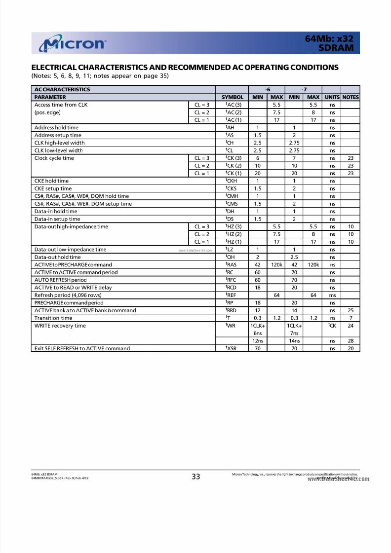
8/11/2019 Mt 48lc2m32b2 - 64mb x32 Sdram
http://slidepdf.com/reader/full/mt-48lc2m32b2-64mb-x32-sdram 33/53
3364Mb: x32 SDRAM Micron Technology, Inc., reserves the right to change products or specifications without notice.
64MSDRAMx32_5.p65 – Rev. B; Pub. 6/02 ©2002, Micron Technology, Inc.
64Mb: x32SDRAM
ELECTRICAL CHARACTERISTICS AND RECOMMENDED AC OPERATING CONDITIONS(Notes: 5, 6, 8, 9, 11; notes appear on page 35)
AC CHARACTERISTICS -6 -7
PARAMETER SYMBOL MIN MAX MIN MAX UNITS NOTESAccess time from CLK CL = 3 tAC (3) 5.5 5.5 ns
(pos. edge) CL = 2 tAC (2) 7.5 8 ns
CL = 1 tAC (1) 17 17 ns
Address hold time tAH 1 1 ns
Address setup time tAS 1.5 2 ns
CLK high-level width tCH 2.5 2.75 ns
CLK low-level width tCL 2.5 2.75 ns
Clock cycle time CL = 3 tCK (3) 6 7 ns 23
CL = 2 tCK (2) 10 10 ns 23
CL = 1 tCK (1) 20 20 ns 23
CKE hold time tCKH 1 1 ns
CKE setup time tCKS 1.5 2 ns
CS#, RAS#, CAS#, WE#, DQM hold time tCMH 1 1 ns
CS#, RAS#, CAS#, WE#, DQM setup time tCMS 1.5 2 ns
Data-in hold time tDH 1 1 ns
Data-in setup time tDS 1.5 2 ns
Data-out high-impedance time CL = 3 tHZ (3) 5.5 5.5 ns 10
CL = 2 tHZ (2) 7.5 8 ns 10
CL = 1 tHZ (1) 17 17 ns 10
Data-out low-impedance time tLZ 1 1 ns
Data-out hold time tOH 2 2.5 ns
ACTIVE to PRECHARGE command tRAS 42 120k 42 120k ns
ACTIVE to ACTIVE command period tRC 60 70 ns
AUTO REFRESH period tRFC 60 70 ns
ACTIVE to READ or WRITE delay tRCD 18 20 ns
Refresh period (4,096 rows) tREF 64 64 ms
PRECHARGE command period tRP 18 20 ns
ACTIVE banka to ACTIVE bankb command tRRD 12 14 ns 25
Transition time tT 0.3 1.2 0.3 1.2 ns 7
WRITE recovery time tWR 1CLK+ 1CLK+ tCK 24
6ns 7ns
12ns 14ns ns 28
Exit SELF REFRESH to ACTIVE command tXSR 70 70 ns 20
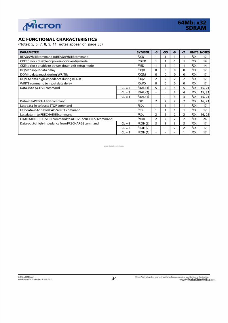
8/11/2019 Mt 48lc2m32b2 - 64mb x32 Sdram
http://slidepdf.com/reader/full/mt-48lc2m32b2-64mb-x32-sdram 34/53
3464Mb: x32 SDRAM Micron Technology, Inc., reserves the right to change products or specifications without notice.
64MSDRAMx32_5.p65 – Rev. B; Pub. 6/02 ©2002, Micron Technology, Inc.
64Mb: x32SDRAM
AC FUNCTIONAL CHARACTERISTICS(Notes: 5, 6, 7, 8, 9, 11; notes appear on page 35)
PARAMETER SYMBOL -5 -55 -6 -7 UNITS NOTES
READ/WRITE command to READ/WRITE command tCCD 1 1 1 1 tCK 17CKE to clock disable or power-down entry mode tCKED 1 1 1 1 tCK 14
CKE to clock enable or power-down exit setup mode tPED 1 1 1 1 tCK 14
DQM to input data delay tDQD 0 0 0 0 tCK 17
DQM to data mask during WRITEs tDQM 0 0 0 0 tCK 17
DQM to data high-impedance during READs tDQZ 2 2 2 2 tCK 17
WRITE command to input data delay tDWD 0 0 0 0 tCK 17
Data-in to ACTIVE command CL = 3 tDAL (3) 5 5 5 5 tCK 15, 21
CL = 2 tDAL (2) - - 4 4 tCK 15, 21
CL = 1 tDAL (1) - - 3 3 tCK 15, 21
Data-in to PRECHARGE command tDPL 2 2 2 2 tCK 16, 21
Last data-in to burst STOP command tBDL 1 1 1 1 tCK 17
Last data-in to new READ/WRITE command tCDL 1 1 1 1 tCK 17
Last data-in to PRECHARGE command tRDL 2 2 2 2 tCK 16, 21
LOAD MODE REGISTER command to ACTIVE or REFRESH command tMRD 2 2 2 2 tCK 26
Data-out to high-impedance from PRECHARGE command CL = 3 tROH (3) 3 3 3 3 tCK 17
CL = 2 tROH (2) - - 2 2 tCK 17
CL = 1 tROH (1) - - – 1 tCK 17
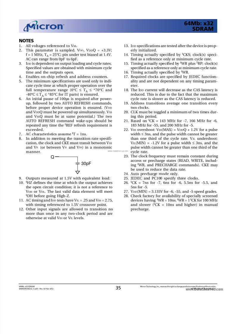
8/11/2019 Mt 48lc2m32b2 - 64mb x32 Sdram
http://slidepdf.com/reader/full/mt-48lc2m32b2-64mb-x32-sdram 35/53
3564Mb: x32 SDRAM Micron Technology, Inc., reserves the right to change products or specifications without notice.
64MSDRAMx32_5.p65 – Rev. B; Pub. 6/02 ©2002, Micron Technology, Inc.
64Mb: x32SDRAM
13. IDD specifications are tested after the device is prop-erly initialized.
14. Timing actually specified by tCKS; clock(s) speci-
fied as a reference only at minimum cycle rate.15. Timing actually specified by t WR plus tRP; clock(s)
specified as a reference only at minimum cycle rate.16. Timing actually specified by t WR.17. Required clocks are specified by JEDEC function-
ality and are not dependent on any timing param-eter.
18. The IDD current will decrease as the CAS latency isreduced. This is due to the fact that the maximumcycle rate is slower as the CAS latency is reduced.
19. Address transitions average one transition every two clocks.
20. CLK must be toggled a minimum of two times dur-
ing this period.21. Based on tCK = 143 MHz for -7, 166 MHz for -6,
183 MHz for -55, and 200 MHz for -5.22. V IH overshoot: V IH(MAX) = V DDQ + 1.2V for a pulse
width ≤ 3ns, and the pulse width cannot be greaterthan one third of the cycle rate. V IL undershoot: V IL(MIN) = -1.2V for a pulse width ≤ 3ns, and thepulse width cannot be greater than one third of thecycle rate.
23. The clock frequency must remain constant during access or precharge states (READ, WRITE, includ-ing t WR, and PRECHARGE commands). CKE may be used to reduce the data rate.
24. Auto precharge mode only.25. JEDEC and PC100 specify three clocks.26. tCK = 7ns for -7, 6ns for -6, 5.5ns for -5.5, and
5ns for -5.27. V DD(MIN) = 3.135V for -6, -55, and -5 speed grades.28. Check factory for availability of specially screened
devices having t WR = 10ns. t WR = 1 tCK for 100 MHzand slower (tCK = 10ns and higher) in manualprecharge.
NOTES1. All voltages referenced to V SS.2. This parameter is sampled. V DD, V DDQ = +3.3V;
f = 1 MHz, T A = 25°C; pin under test biased at 1.4V.
AC can range from 0pF to 6pF.3. IDD is dependent on output loading and cycle rates.
Specified values are obtained with minimum cycletime and the outputs open.
4. Enables on-chip refresh and address counters.5. The minimum specifications are used only to indi-
cate cycle time at which proper operation over thefull temperature range (0°C ≤ T A ≤ +70°C and-40°C ≤ T A ≤ +85°C for IT parts) is ensured.
6. An initial pause of 100µs is required after power-up, followed by two AUTO REFRESH commands,before proper device operation is ensured. (V DD
and V DDQ must be powered up simultaneously. V SS
and V SSQ must be at same potential.) The two AUTO REFRESH command wake-ups should berepeated any time the tREF refresh requirement isexceeded.
7. AC characteristics assume tT = 1ns.8. In addition to meeting the transition rate specifi-
cation, the clock and CKE must transit between V IH
and V IL (or between V IL and V IH) in a monotonicmanner.
9. Outputs measured at 1.5V with equivalent load:10. tHZ defines the time at which the output achieves
the open circuit condition; it is not a reference to V OH or V OL. The last valid data element will meettOH before going High-Z.
11. AC timing and IDD tests have V IL = .25 and V IH = 2.75, with timing referenced to 1.5V crossover point.
12. Other input signals are allowed to transition nomore than once in any two-clock period and areotherwise at valid V IH or V IL levels.
Q
30pF
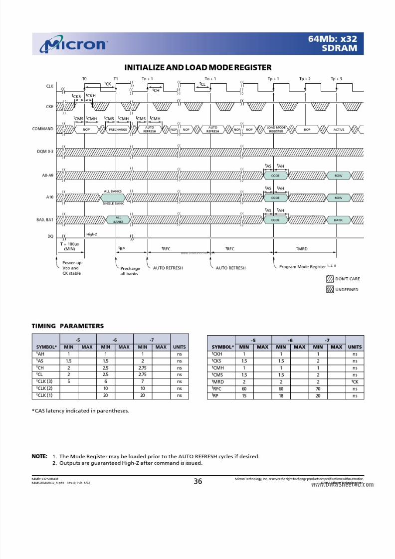
8/11/2019 Mt 48lc2m32b2 - 64mb x32 Sdram
http://slidepdf.com/reader/full/mt-48lc2m32b2-64mb-x32-sdram 36/53
8/11/2019 Mt 48lc2m32b2 - 64mb x32 Sdram
http://slidepdf.com/reader/full/mt-48lc2m32b2-64mb-x32-sdram 37/53
3764Mb: x32 SDRAM Micron Technology, Inc., reserves the right to change products or specifications without notice.
64MSDRAMx32_5.p65 – Rev. B; Pub. 6/02 ©2002, Micron Technology, Inc.
64Mb: x32SDRAM
NOTE: 1. Violating refresh requirements during power-down may result in a loss of data.
POWER-DOWN MODE 1
*CAS latency indicated in parentheses.
-5 -6 -7
SYMBOL* MIN MAX MIN MAX MIN MAX UNITStCK (1) 20 20 nstCKH 1 1 1 nstCKS 1.5 1.5 2 nstCMH 1 1 1 nstCMS 1.5 1.5 2 ns
TIMING PARAMETERS
-5 -6 -7
SYMBOL* MIN MAX MIN MAX MIN MAX UNITStAH 1 1 1 nstAS 1.5 1.5 2 nstCH 2 2.5 2.75 nstCL 2 2.5 2.75 nstCK (3) 5 6 7 nstCK (2) 10 10 ns
tCH
tCLtCK
Two clock cycles
CKE
CLK
DQ
All banks idle, enterpower-down mode
Precharge allactive banks
Input buffers gated off while in
power-down mode
Exit power-down mode
()()
()()
tCKS tCKS
COMMAND
tCMHtCMS
PRECHARGE NOP NOP ACTIVENOP
()()
()()
All banks idle
BA0, BA1 BANKBANK(S)
()()
()()
High-Z
tAHtAS
tCKHtCKS
DQM 0-3
()()
()()
()()
(
)
(
)
A0-A9 ROW
()()
()()
ALL BANKS
SINGLE BANK
A10 ROW
()()
()()
T0 T1 T2 Tn + 1 Tn + 2
DON’T CARE
UNDEFINED
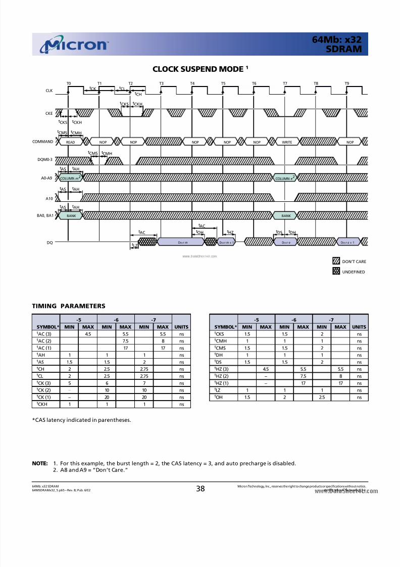
8/11/2019 Mt 48lc2m32b2 - 64mb x32 Sdram
http://slidepdf.com/reader/full/mt-48lc2m32b2-64mb-x32-sdram 38/53
3864Mb: x32 SDRAM Micron Technology, Inc., reserves the right to change products or specifications without notice.
64MSDRAMx32_5.p65 – Rev. B; Pub. 6/02 ©2002, Micron Technology, Inc.
64Mb: x32SDRAM
CLOCK SUSPEND MODE 1
NOTE: 1. For this example, the burst length = 2, the CAS latency = 3, and auto precharge is disabled.2. A8 and A9 = “Don’t Care.”
*CAS latency indicated in parentheses.
-5 -6 -7
SYMBOL* MIN MAX MIN MAX MIN MAX UNITStCKS 1.5 1.5 2 nstCMH 1 1 1 nstCMS 1.5 1.5 2 nstDH 1 1 1 nstDS 1.5 1.5 2 nstHZ (3) 4.5 5.5 5.5 nstHZ (2) – 7.5 8 nstHZ (1) – 17 17 nstLZ 1 1 1 ns
tOH 1.5 2 2.5 ns
TIMING PARAMETERS
-5 -6 -7
SYMBOL* MIN MAX MIN MAX MIN MAX UNITStAC (3) 4.5 5.5 5.5 nstAC (2) 7.5 8 nstAC (1) 17 17 nstAH 1 1 1 nstAS 1.5 1.5 2 nstCH 2 2.5 2.75 nstCL 2 2.5 2.75 nstCK (3) 5 6 7 nstCK (2) – 10 10 ns
tCK (1) – 20 20 nstCKH 1 1 1 ns
tCH
tCLtCK
tAC
tLZ
DQM0-3
CLK
DQ
A10
tOH
DOUT m
tAHtAS
tAHtAS
tAHtAS
BANK
tDH
DOUT e
tAC
tHZ
DOUT m + 1
COMMAND
tCMHtCMS
NOPNOP NOP NOPNOPREAD WRITE
DON’T CARE
UNDEFINED
CKE
tCKS tCKH
BANK
COLUMNm
tDS
DOUT e + 1
NOP
tCKHtCKS
tCMHtCMS
2COLUMN e
2
T0 T1 T2 T3 T4 T5 T6 T7 T8 T9
BA0, BA1
A0-A9
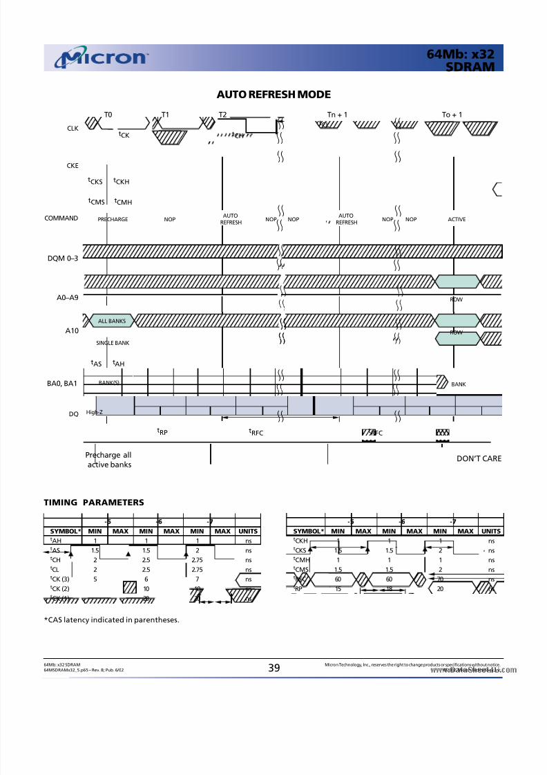
8/11/2019 Mt 48lc2m32b2 - 64mb x32 Sdram
http://slidepdf.com/reader/full/mt-48lc2m32b2-64mb-x32-sdram 39/53
3964Mb: x32 SDRAM Micron Technology, Inc., reserves the right to change products or specifications without notice.
64MSDRAMx32_5.p65 – Rev. B; Pub. 6/02 ©2002, Micron Technology, Inc.
64Mb: x32SDRAM
AUTO REFRESH MODE
*CAS latency indicated in parentheses.
-5 -6 -7
SYMBOL* MIN MAX MIN MAX MIN MAX UNITSt
CKH 1 1 1 nstCKS 1.5 1.5 2 nstCMH 1 1 1 nstCMS 1.5 1.5 2 nstRFC 60 60 70 nstRP 15 18 20 ns
TIMING PARAMETERS
-5 -6 -7
SYMBOL* MIN MAX MIN MAX MIN MAX UNITSt
AH 1 1 1 nstAS 1.5 1.5 2 nstCH 2 2.5 2.75 nstCL 2 2.5 2.75 nstCK (3) 5 6 7 nstCK (2) 10 10 nstCK (1) 20 20 ns
UNDEFINEDDON’T CARE
tCH
tCL
tCK
CKE
CLK
DQ
tRFC
()()
()()
()()
tRP
()()
()()
()()
()()
COMMAND
tCMHtCMS
NOPNOP
()()
()()
BANK
ACTIVEAUTO
REFRESH
()()
()()
NOPNOPPRECHARGE
Precharge all
active banks
AUTO REFRESH
tRFC
High-Z
BANK(S)
()()
()()
()()
()()
tAHtAS
tCKHtCKS
()()
NOP
()()
()()
()()
(
)
(
)
ROW
()()
()()
ALL BANKS
SINGLE BANK
A10 ROW
()()
()()
()()
()()
()()
()()
()()
()()
T0 T1 T2 Tn + 1 To + 1
BA0, BA1
A0–A9
DQM 0–3
DON’T CARE
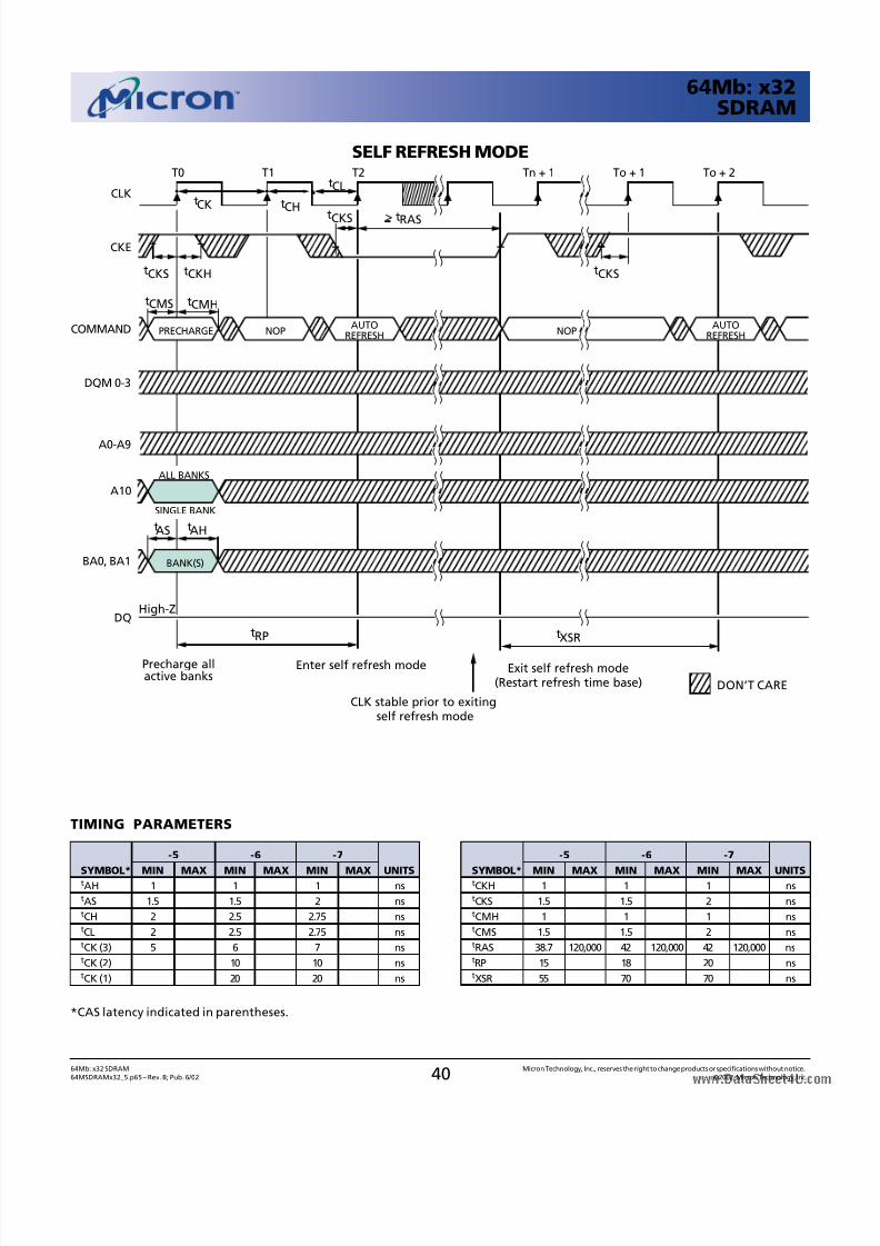
8/11/2019 Mt 48lc2m32b2 - 64mb x32 Sdram
http://slidepdf.com/reader/full/mt-48lc2m32b2-64mb-x32-sdram 40/53
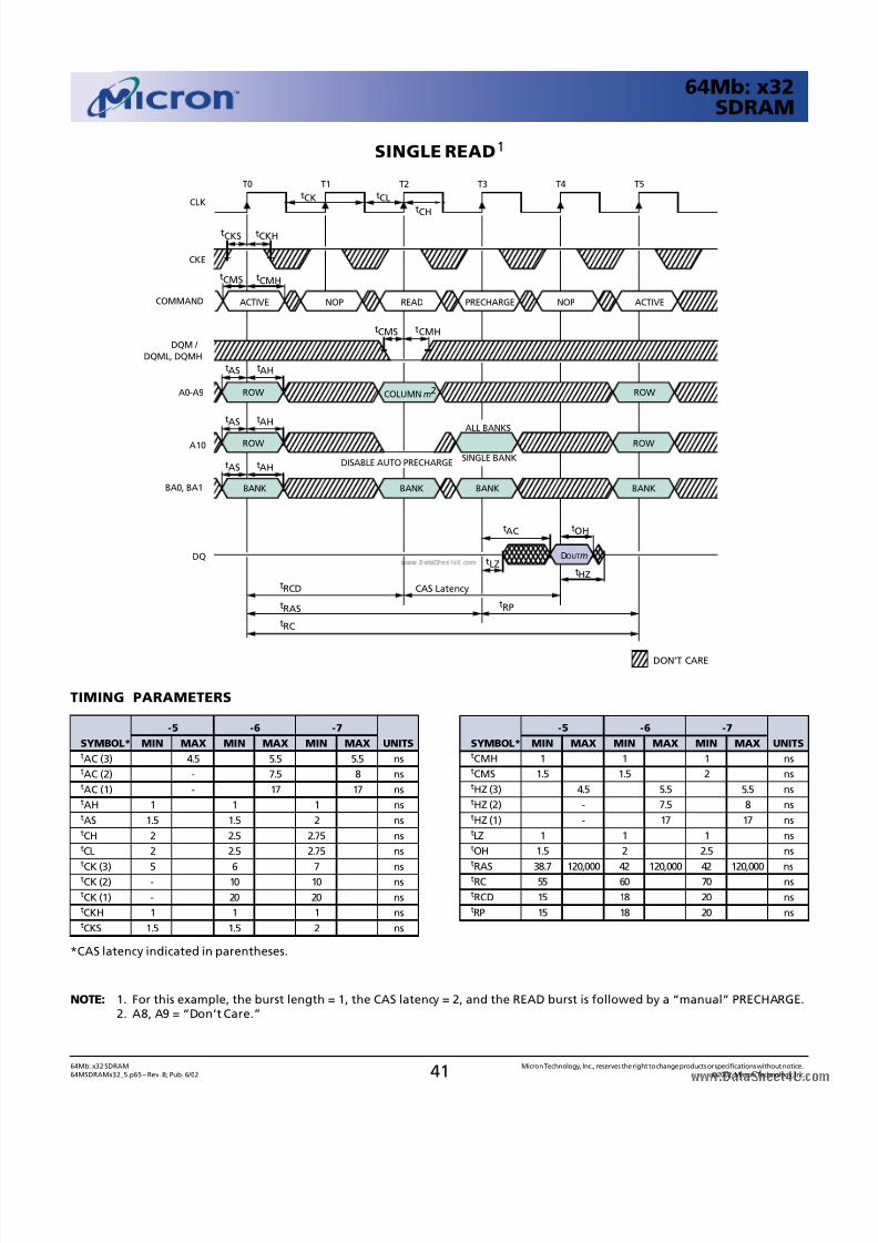
8/11/2019 Mt 48lc2m32b2 - 64mb x32 Sdram
http://slidepdf.com/reader/full/mt-48lc2m32b2-64mb-x32-sdram 41/53
4164Mb: x32 SDRAM Micron Technology, Inc., reserves the right to change products or specifications without notice.
64MSDRAMx32_5.p65 – Rev. B; Pub. 6/02 ©2002, Micron Technology, Inc.
64Mb: x32SDRAM
SINGLE READ1
*CAS latency indicated in parentheses.
ALL BANKS
tCH
tCLtCK
tAC
tLZ
tRPtRAS
tRCD CAS Latency
tRC
DQM /
DQML, DQMH
CKE
CLK
A0-A9
DQ
BA0, BA1
A10
tOH
DOUTm
tCMHtCMS
tAHtAS
tAHtAS
tAHtAS
ROW
ROW
BANK BANK BANK
ROW
ROW
BANK
tHZ
COMMAND
tCMHtCMS
PRECHARGEACTIVE NOP READ NOP ACTIVE
DISABLE AUTO PRECHARGESINGLE BANK
tCKHtCKS
COLUMNm2
T0 T1 T2 T4T3 T5
DON’T CARE
NOTE: 1. For this example, the burst length = 1, the CAS latency = 2, and the READ burst is followed by a “manual” PRECHARGE.2. A8, A9 = “Don’t Care.”
TIMING PARAMETERS
-5 -6 -7
SYMBOL* MIN MAX MIN MAX MIN MAX UNITStAC (3) 4.5 5.5 5.5 nstAC (2) - 7.5 8 nstAC (1) - 17 17 nstAH 1 1 1 nstAS 1.5 1.5 2 nstCH 2 2.5 2.75 nstCL 2 2.5 2.75 nst
CK (3) 5 6 7 nstCK (2) - 10 10 nstCK (1) - 20 20 nstCKH 1 1 1 nstCKS 1.5 1.5 2 ns
tCMH 1 1 1 nstCMS 1.5 1.5 2 nstHZ (3) 4.5 5.5 5.5 nstHZ (2) - 7.5 8 nstHZ (1) - 17 17 nstLZ 1 1 1 nstOH 1.5 2 2.5 nst
RAS 38.7 120,000 42 120,000 42 120,000 nstRC 55 60 70 nstRCD 15 18 20 nstRP 15 18 20 ns
-5 -6 -7
SYMBOL* MIN MAX MIN MAX MIN MAX UNITS
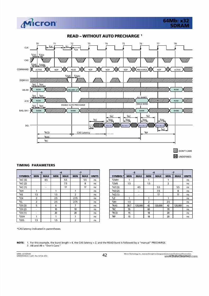
8/11/2019 Mt 48lc2m32b2 - 64mb x32 Sdram
http://slidepdf.com/reader/full/mt-48lc2m32b2-64mb-x32-sdram 42/53
4264Mb: x32 SDRAM Micron Technology, Inc., reserves the right to change products or specifications without notice.
64MSDRAMx32_5.p65 – Rev. B; Pub. 6/02 ©2002, Micron Technology, Inc.
64Mb: x32SDRAM
READ – WITHOUT AUTO PRECHARGE 1
NOTE: 1. For this example, the burst length = 4, the CAS latency = 2, and the READ burst is followed by a “manual” PRECHARGE.2. A8 and A9 = “Don’t Care.”
*CAS latency indicated in parentheses.
-5 -6 -7
SYMBOL* MIN MAX MIN MAX MIN MAX UNITStCMH 1 1 1 nstCMS 1.5 1.5 2 nstHZ (3) 4.5 5.5 5.5 nstHZ (2) - 7.5 8 nstHZ (1) - 17 17 nstLZ 1 1 1 nstOH 1.5 2 2.5 nstRAS 38.7 120,000 42 120,000 42 120,000 nstRC 55 60 70 nstRCD 15 18 20 nstRP 15 18 20 ns
TIMING PARAMETERS
-5 -6 -7
SYMBOL* MIN MAX MIN MAX MIN MAX UNITStAC (3) 4.5 5.5 5.5 nstAC (2) - 7.5 8 nstAC (1) - 17 17 nstAH 1 1 1 nstAS 1.5 1.5 2 nstCH 2 2.5 2.75 nstCL 2 2.5 2.75 nstCK (3) 5 6 7 nstCK (2) - 10 10 nstCK (1) - 20 20 nstCKH 1 1 1 nstCKS 1.5 1.5 2 ns
ALL BANKS
tCH
tCLtCK
tAC
tLZ
tRP
tRAS
tRCD CAS Latency
tRC
CKE
CLK
DQ
A10
tOH
DOUT m
tCMHtCMS
tAHtAS
tAHtAS
tAHtAS
ROW
ROW
BANK BANK BANK
ROW
ROW
BANK
tHZ
tOH
DOUT m + 3
tAC
tOH
tAC
tOH
tAC
DOUT m + 2DOUT m + 1
COMMAND
tCMHtCMS
PRECHARGENOPNOP NOPACTIVE NOP READ NOP ACTIVE
DISABLE AUTO PRECHARGE SINGLE BANK
DON’T CARE
UNDEFINED
tCKHtCKS
COLUMN m2
T0 T1 T2 T4T3 T5 T6 T7 T8
BA0, BA1
DQM 0-3
A0-A9
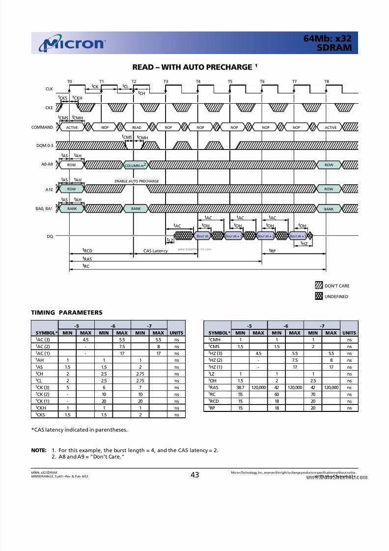
8/11/2019 Mt 48lc2m32b2 - 64mb x32 Sdram
http://slidepdf.com/reader/full/mt-48lc2m32b2-64mb-x32-sdram 43/53
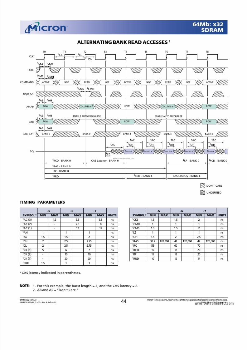
8/11/2019 Mt 48lc2m32b2 - 64mb x32 Sdram
http://slidepdf.com/reader/full/mt-48lc2m32b2-64mb-x32-sdram 44/53
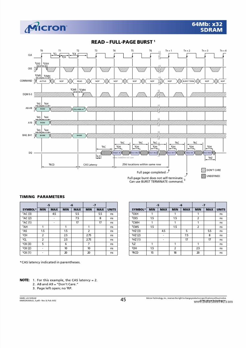
8/11/2019 Mt 48lc2m32b2 - 64mb x32 Sdram
http://slidepdf.com/reader/full/mt-48lc2m32b2-64mb-x32-sdram 45/53
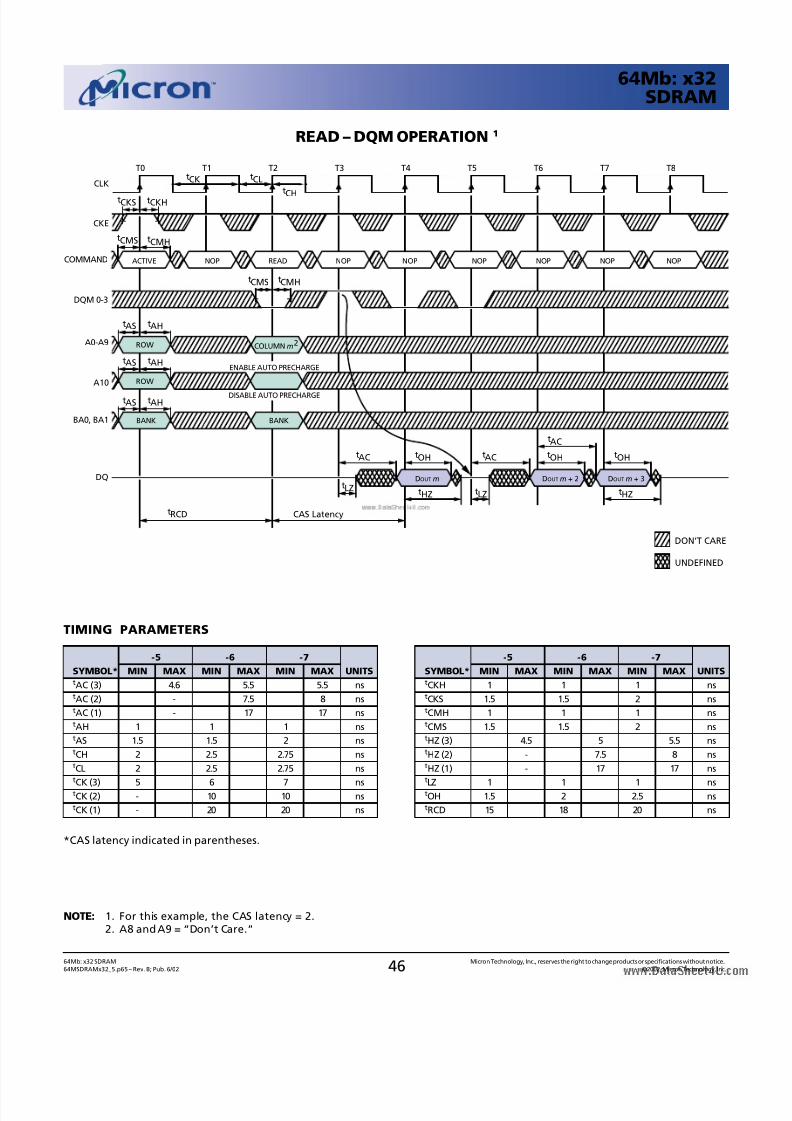
8/11/2019 Mt 48lc2m32b2 - 64mb x32 Sdram
http://slidepdf.com/reader/full/mt-48lc2m32b2-64mb-x32-sdram 46/53
4664Mb: x32 SDRAM Micron Technology, Inc., reserves the right to change products or specifications without notice.
64MSDRAMx32_5.p65 – Rev. B; Pub. 6/02 ©2002, Micron Technology, Inc.
64Mb: x32SDRAM
READ – DQM OPERATION 1
tCH
tCLtCK
tRCD CAS Latency
CKE
CLK
DQ
A10
tCMS
ROW
BANK
ROW
BANK
DON’T CARE
UNDEFINED
tAC
LZDOUT m
tOH
DOUT m + 3DOUT m + 2t
tHZ LZt
tCMH
COMMAND NOPNOP NOPACTIVE NOP READ NOPNOP NOP
tHZ
tAC tOH
tAC
tOH
tAHtAS
tCMS tCMH
tAHtAS
tAHtAS
tCKHtCKS
ENABLE AUTO PRECHARGE
DISABLE AUTO PRECHARGE
COLUMNm2
T0 T1 T2 T4T3 T5 T6 T7 T8
BA0, BA1
DQM 0-3
A0-A9
NOTE: 1. For this example, the CAS latency = 2.2. A8 and A9 = “Don’t Care.”
*CAS latency indicated in parentheses.
-5 -6 -7
SYMBOL* MIN MAX MIN MAX MIN MAX UNITStCKH 1 1 1 nstCKS 1.5 1.5 2 nstCMH 1 1 1 nstCMS 1.5 1.5 2 nstHZ (3) 4.5 5 5.5 nstHZ (2) - 7.5 8 nstHZ (1) - 17 17 nst
LZ 1 1 1 nstOH 1.5 2 2.5 nstRCD 15 18 20 ns
TIMING PARAMETERS
-5 -6 -7
SYMBOL* MIN MAX MIN MAX MIN MAX UNITStAC (3) 4.6 5.5 5.5 nstAC (2) - 7.5 8 nstAC (1) - 17 17 nstAH 1 1 1 nstAS 1.5 1.5 2 nstCH 2 2.5 2.75 nstCL 2 2.5 2.75 nst
CK (3) 5 6 7 nstCK (2) - 10 10 nstCK (1) - 20 20 ns
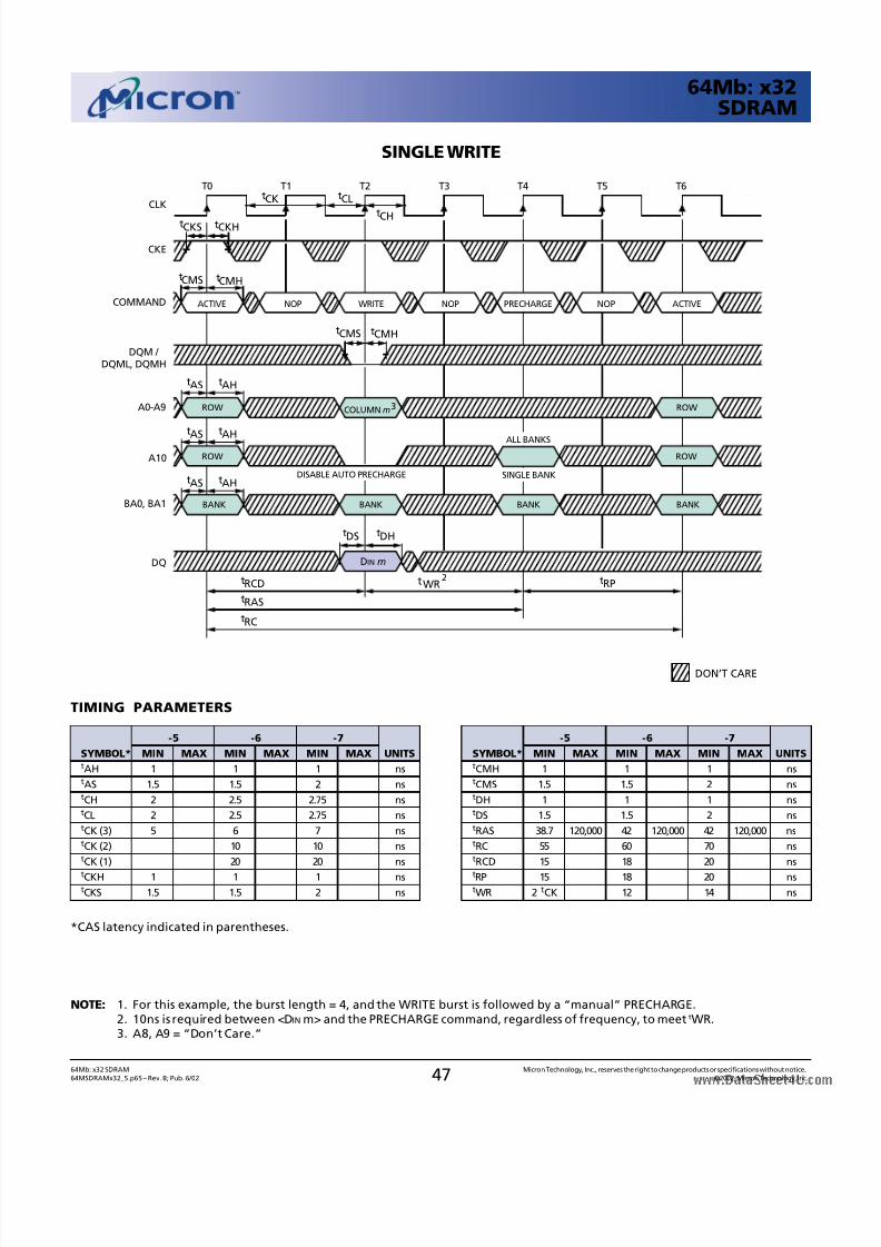
8/11/2019 Mt 48lc2m32b2 - 64mb x32 Sdram
http://slidepdf.com/reader/full/mt-48lc2m32b2-64mb-x32-sdram 47/53
4764Mb: x32 SDRAM Micron Technology, Inc., reserves the right to change products or specifications without notice.
64MSDRAMx32_5.p65 – Rev. B; Pub. 6/02 ©2002, Micron Technology, Inc.
64Mb: x32SDRAM
SINGLE WRITE
TIMING PARAMETERS
-5 -6 -7
SYMBOL* MIN MAX MIN MAX MIN MAX UNITStAH 1 1 1 nstAS 1.5 1.5 2 nstCH 2 2.5 2.75 nstCL 2 2.5 2.75 nstCK (3) 5 6 7 nstCK (2) 10 10 nstCK (1) 20 20 ns
tCKH 1 1 1 nstCKS 1.5 1.5 2 ns
tCMH 1 1 1 nstCMS 1.5 1.5 2 nstDH 1 1 1 nstDS 1.5 1.5 2 nstRAS 38.7 120,000 42 120,000 42 120,000 nstRC 55 60 70 nstRCD 15 18 20 ns
tRP 15 18 20 nstWR 2 tCK 12 14 ns
*CAS latency indicated in parentheses.
DON’T CARE
DISABLE AUTO PRECHARGE
ALL BANKS
tCH
tCLtCK
tRP
tRAS
tRCD
tRC
DQM /DQML, DQMH
CKE
CLK
A0-A9
DQ
BA0, BA1
A10
tCMHtCMS
tAHtAS
ROW
ROW
BANK BANK BANK
ROW
ROW
BANK
tWR
DIN m
tDHtDS
COMMAND
tCMHtCMS
ACTIVE NOP WRITE NOP PRECHARGE ACTIVE
tAH
tAS
tAHtAS
SINGLE BANK
tCKHtCKS
COLUMNm3
2
T0 T1 T2 T4T3 T5 T6
NOP
-5 -6 -7
SYMBOL* MIN MAX MIN MAX MIN MAX UNITS
NOTE: 1. For this example, the burst length = 4, and the WRITE burst is followed by a “manual” PRECHARGE.2. 10ns is required between <DIN m> and the PRECHARGE command, regardless of frequency, to meet tWR.3. A8, A9 = “Don’t Care.”
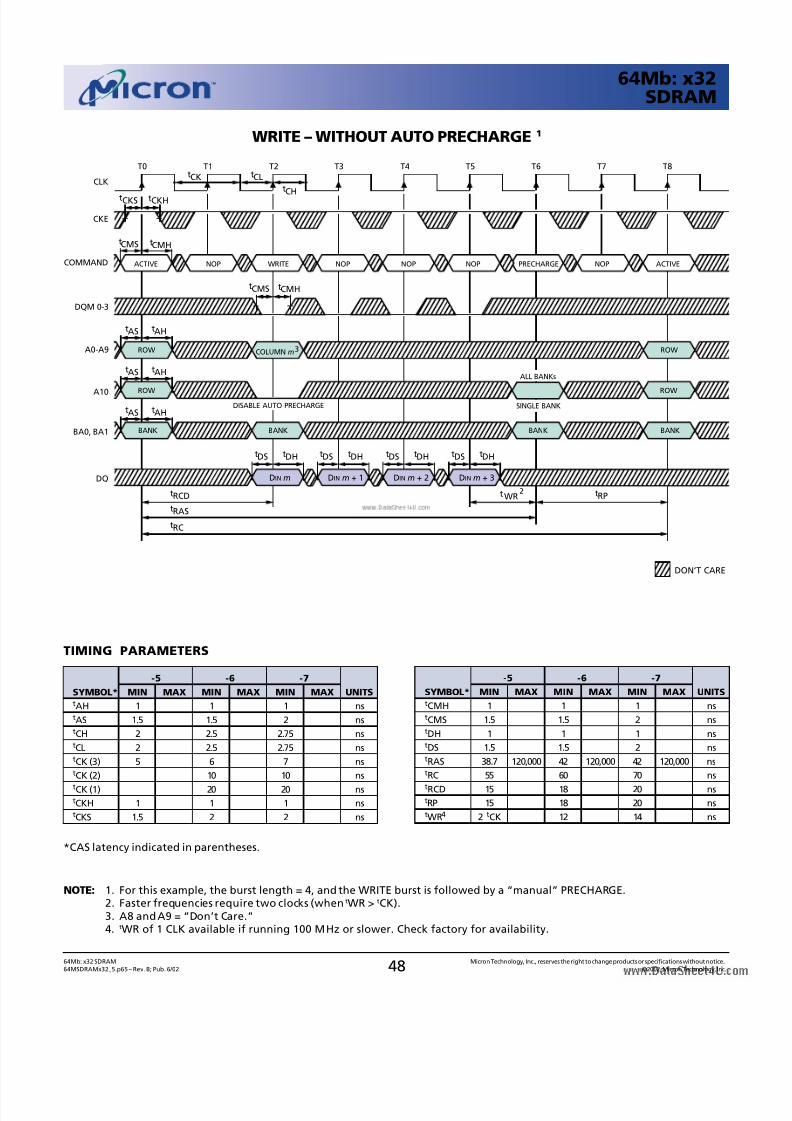
8/11/2019 Mt 48lc2m32b2 - 64mb x32 Sdram
http://slidepdf.com/reader/full/mt-48lc2m32b2-64mb-x32-sdram 48/53
4864Mb: x32 SDRAM Micron Technology, Inc., reserves the right to change products or specifications without notice.
64MSDRAMx32_5.p65 – Rev. B; Pub. 6/02 ©2002, Micron Technology, Inc.
64Mb: x32SDRAM
WRITE – WITHOUT AUTO PRECHARGE 1
NOTE: 1. For this example, the burst length = 4, and the WRITE burst is followed by a “manual” PRECHARGE.2. Faster frequencies require two clocks (when tWR > tCK).3. A8 and A9 = “Don’t Care.”4. tWR of 1 CLK available if running 100 MHz or slower. Check factory for availability.
*CAS latency indicated in parentheses.
-5 -6 -7
SYMBOL* MIN MAX MIN MAX MIN MAX UNITStCMH 1 1 1 nstCMS 1.5 1.5 2 nstDH 1 1 1 nstDS 1.5 1.5 2 nstRAS 38.7 120,000 42 120,000 42 120,000 nstRC 55 60 70 ns
tRCD 15 18 20 nstRP 15 18 20 nstWR4 2 tCK 12 14 ns
TIMING PARAMETERS
-5 -6 -7
SYMBOL* MIN MAX MIN MAX MIN MAX UNITStAH 1 1 1 nstAS 1.5 1.5 2 nstCH 2 2.5 2.75 nstCL 2 2.5 2.75 nstCK (3) 5 6 7 nstCK (2) 10 10 ns
tCK (1) 20 20 nstCKH 1 1 1 nstCKS 1.5 2 2 ns
DISABLE AUTO PRECHARGE
ALL BANKs
tCH
tCLtCK
tRP
tRAS
tRCD
tRC
CKE
CLK
DQ
A10
tCMHtCMS
tAHtAS
ROW
ROW
BANK BANK BANK
ROW
ROW
BANK
tWR
DON’T CARE
DIN m
tDHtDS
DIN m + 1 DIN m + 2 DIN m + 3
COMMAND
tCMHtCMS
NOPNOP NOPACTIVE NOP WRITE NOPPRECHARGE ACTIVE
tAHtAS
tAHtAS
tDHtDS tDHtDS tDHtDS
SINGLE BANK
tCKHtCKS
COLUMN m3
2
T0 T1 T2 T4T3 T5 T6 T7 T8
DQM 0-3
BA0, BA1
A0-A9
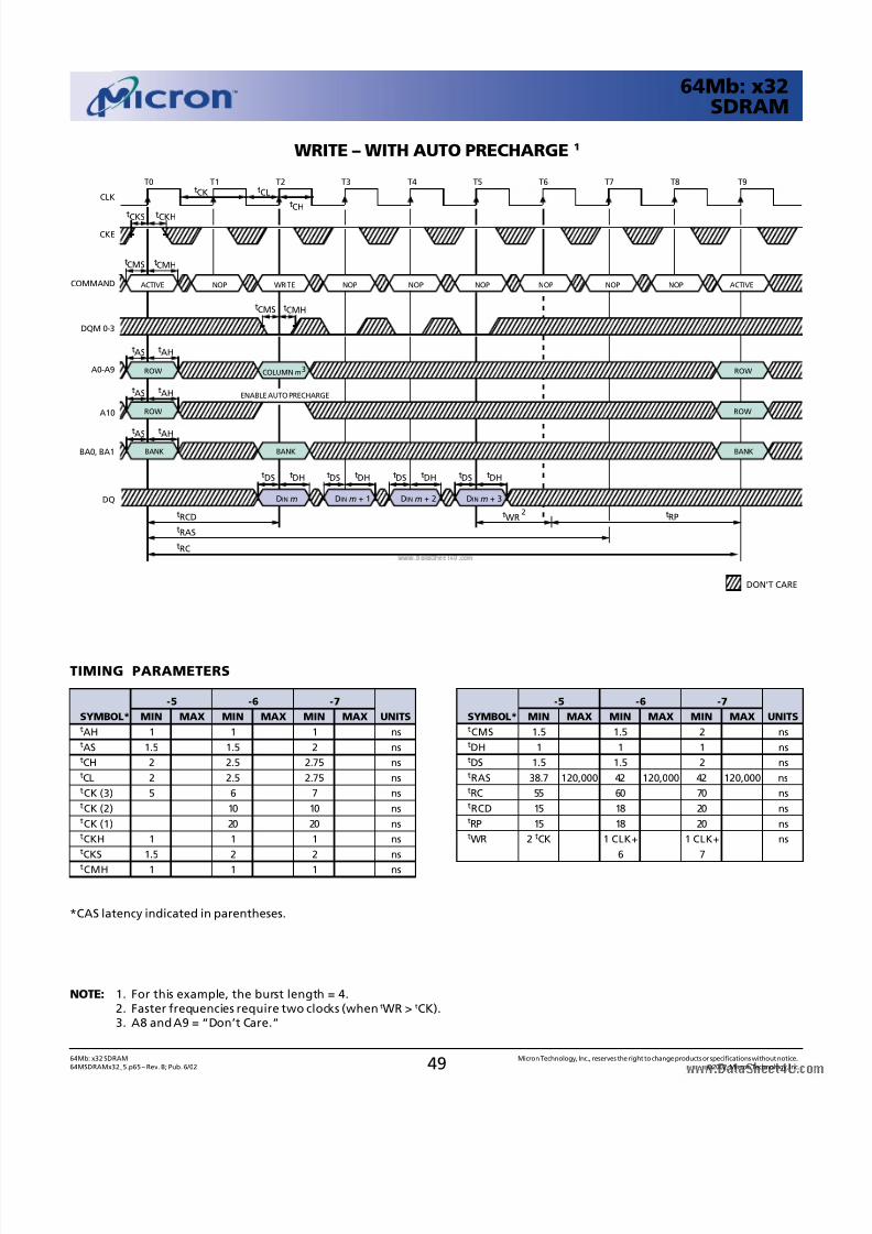
8/11/2019 Mt 48lc2m32b2 - 64mb x32 Sdram
http://slidepdf.com/reader/full/mt-48lc2m32b2-64mb-x32-sdram 49/53
4964Mb: x32 SDRAM Micron Technology, Inc., reserves the right to change products or specifications without notice.
64MSDRAMx32_5.p65 – Rev. B; Pub. 6/02 ©2002, Micron Technology, Inc.
64Mb: x32SDRAM
tCMS 1.5 1.5 2 nstDH 1 1 1 nstDS 1.5 1.5 2 nstRAS 38.7 120,000 42 120,000 42 120,000 nstRC 55 60 70 nstRCD 15 18 20 nstRP 15 18 20 nstWR 2 tCK 1 CLK+ 1 CLK+ ns
6 7
WRITE – WITH AUTO PRECHARGE 1
NOTE: 1. For this example, the burst length = 4.2. Faster frequencies require two clocks (when tWR > tCK).3. A8 and A9 = “Don’t Care.”
*CAS latency indicated in parentheses.
-5 -6 -7
SYMBOL* MIN MAX MIN MAX MIN MAX UNITS
TIMING PARAMETERS
-5 -6 -7
SYMBOL* MIN MAX MIN MAX MIN MAX UNITStAH 1 1 1 nstAS 1.5 1.5 2 nstCH 2 2.5 2.75 nstCL 2 2.5 2.75 nstCK (3) 5 6 7 nstCK (2) 10 10 nstCK (1) 20 20 nstCKH 1 1 1 nstCKS 1.5 2 2 ns
tCMH 1 1 1 ns
DON’T CARE
ENABLE AUTO PRECHARGE
tCH
tCLtCK
tRP
tRAS
tRCD
tRC
CKE
CLK
DQ
A10
tCMHtCMS
tAHtAS
ROW
ROW
BANK BANK
ROW
ROW
BANK
tWR
DIN m
tDHtDS
DIN m + 1 DIN m + 2 DIN m + 3
COMMAND
tCMHtCMS
NOPNOP NOPACTIVE NOP WRITE NOP ACTIVE
tAHtAS
tAHtAS
tDHtDS tDHtDS tDHtDS
tCKHtCKS
NOP NOP
COLUMNm3
2
T0 T1 T2 T4T3 T5 T6 T7 T8 T9
BA0, BA1
DQM 0-3
A0-A9
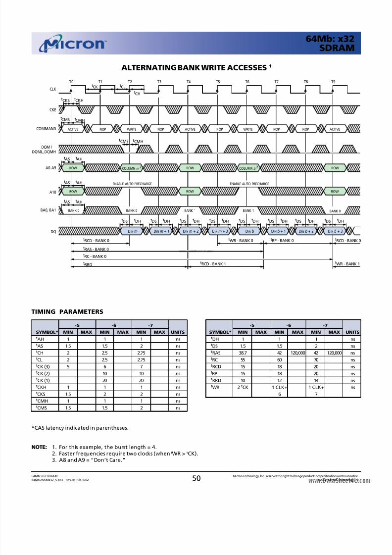
8/11/2019 Mt 48lc2m32b2 - 64mb x32 Sdram
http://slidepdf.com/reader/full/mt-48lc2m32b2-64mb-x32-sdram 50/53
5064Mb: x32 SDRAM Micron Technology, Inc., reserves the right to change products or specifications without notice.
64MSDRAMx32_5.p65 – Rev. B; Pub. 6/02 ©2002, Micron Technology, Inc.
64Mb: x32SDRAM
ALTERNATING BANK WRITE ACCESSES 1
tCH
tCLtCKCLK
DQ DIN m
tDHtDS
DIN m + 1 DIN m + 2 DIN m + 3
COMMAND
tCMHtCMS
NOP NOPACTIVE NOP WRITE NOP NOP ACTIVE
tDHtDS tDHtDS tDHtDS
ACTIVE WRITE
DIN b
tDHtDS
DIN b + 1 DIN b + 3
tDHtDS tDHtDS
ENABLE AUTO PRECHARGE
DQM /
DQML, DQMH
A0-A9
BA0, BA1
A10
tCMHtCMS
tAHtAS
tAHtAS
tAHtAS
ROW
ROW
ROW
ROW
ENABLE AUTO PRECHARGE
ROW
ROW
BANK 0 BANK 0 BANK 1 BANK 0BANK 1
CKE
tCKHtCKS
DIN b + 2
tDHtDS
COLUMNb 2COLUMN m2
tRP - BANK 0
tRAS - BANK 0
tRCD - BANK 0 t
t
RCD - BANK 0tWR - BANK 0
WR - BANK 1tRCD - BANK 1
t
t
RC - BANK 0
RRD
T0 T1 T2 T3 T4 T5 T6 T7 T8 T9
NOTE: 1. For this example, the burst length = 4.2. Faster frequencies require two clocks (when tWR > tCK).3. A8 and A9 = “Don’t Care.”
*CAS latency indicated in parentheses.
-5 -6 -7
SYMBOL* MIN MAX MIN MAX MIN MAX UNITStDH 1 1 1 nstDS 1.5 1.5 2 nstRAS 38.7 42 120,000 42 120,000 nstRC 55 60 70 nstRCD 15 18 20 nstRP 15 18 20 nstRRD 10 12 14 nst
WR 2t
CK 1 CLK+ 1 CLK+ ns6 7
TIMING PARAMETERS
-5 -6 -7
SYMBOL* MIN MAX MIN MAX MIN MAX UNITStAH 1 1 1 nstAS 1.5 1.5 2 nstCH 2 2.5 2.75 nstCL 2 2.5 2.75 nstCK (3) 5 6 7 nstCK (2) 10 10 nstCK (1) 20 20 nst
CKH 1 1 1 nstCKS 1.5 2 2 nstCMH 1 1 1 nstCMS 1.5 1.5 2 ns
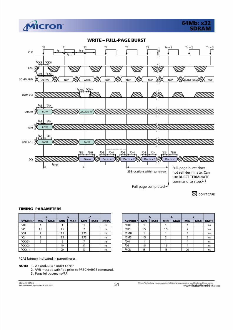
8/11/2019 Mt 48lc2m32b2 - 64mb x32 Sdram
http://slidepdf.com/reader/full/mt-48lc2m32b2-64mb-x32-sdram 51/53
5164Mb: x32 SDRAM Micron Technology, Inc., reserves the right to change products or specifications without notice.
64MSDRAMx32_5.p65 – Rev. B; Pub. 6/02 ©2002, Micron Technology, Inc.
64Mb: x32SDRAM
WRITE – FULL-PAGE BURST
NOTE: 1. A8 and A9 = “Don’t Care.”2. tWR must be satisfied prior to PRECHARGE command.3. Page left open; no tRP.
*CAS latency indicated in parentheses.
-5 -6 -7
SYMBOL* MIN MAX MIN MAX MIN MAX UNITStCKH 1 1 1 nstCKS 1.5 1.5 2 nstCMH 1 1 1 nstCMS 1.5 2 2 nstDH 1 1 1 nstDS 1.5 1.5 2 nstRCD 15 18 20 ns
TIMING PARAMETERS
-5 -6 -7
SYMBOL* MIN MAX MIN MAX MIN MAX UNITStAH 1 1 1 nstAS 1.5 1.5 2 nstCH 2 2.5 2.75 nstCL 2 2.5 2.75 nstCK (3) 5 6 7 nstCK (2) 10 10 nstCK (1) 20 20 ns
tCH
tCL tCK
tRCD
CKE
CLK
A10
tCMS
tAHtAS
tAHtAS
ROW
ROW
Full-page burst does
not self-terminate. Canuse BURST TERMINATE
command to stop.2, 3
()()
()()
()()
(
)
(
)
Full page completed
DON’T CARE
COMMAND
tCMHtCMS
NOPNOP NOPACTIVE NOP WRITE BURST TERMNOP NOP
()()
()()
()()
()()
DQ DIN m
tDHtDS
DIN m + 1 DIN m + 2 DIN m + 3
tDHtDS tDHtDS tDHtDS
DIN m - 1
tDHtDS
tAHtAS
BANK
()()
()()
BANK
tCMH
tCKHtCKS
()()
()()
()()
()()
()()
()()
256 locations within same row
COLUMN m1
T0 T1 T2 T3 T4 T5 Tn + 1 Tn + 2 Tn + 3
BA0, BA1
DQM 0-3
A0-A9
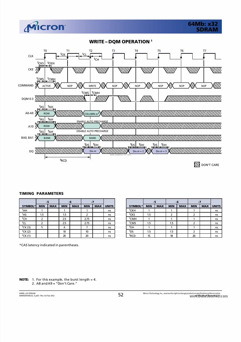
8/11/2019 Mt 48lc2m32b2 - 64mb x32 Sdram
http://slidepdf.com/reader/full/mt-48lc2m32b2-64mb-x32-sdram 52/53
5264Mb: x32 SDRAM Micron Technology, Inc., reserves the right to change products or specifications without notice.
64MSDRAMx32_5.p65 – Rev. B; Pub. 6/02 ©2002, Micron Technology, Inc.
64Mb: x32SDRAM
WRITE – DQM OPERATION 1
NOTE: 1. For this example, the burst length = 4.2. A8 and A9 = “Don’t Care.”
*CAS latency indicated in parentheses.
-5 -6 -7
SYMBOL* MIN MAX MIN MAX MIN MAX UNITStCKH 1 1 1 nstCKS 1.5 2 2 nstCMH 1 1 1 nstCMS 1.5 1.5 2 nstDH 1 1 1 nstDS 1.5 1.5 2 nstRCD 15 18 20 ns
TIMING PARAMETERS
-5 -6 -7
SYMBOL* MIN MAX MIN MAX MIN MAX UNITStAH 1 1 1 nstAS 1.5 1.5 2 nstCH 2 2.5 2.75 nstCL 2 2.5 2.75 nstCK (3) 5 6 7 nstCK (2) 10 10 nstCK (1) 20 20 ns
DON’T CARE
tCH
tCLtCK
tRCD
CKE
CLK
DQ
A10
tCMS
tAHtAS
ROW
BANK
ROW
BANK
ENABLE AUTO PRECHARGE
DIN m + 3
tDHtDS
DIN m DIN m + 2
tCMH
COMMAND NOPNOP NOPACTIVE NOP WRITE NOPNOP
tCMS tCMH
tDHtDStDHtDS
tAHtAS
tAHtAS
DISABLE AUTO PRECHARGE
tCKHtCKS
COLUMN m2
T0 T1 T2 T3 T4 T5 T6 T7
BA0, BA1
DQM 0-3
A0-A9
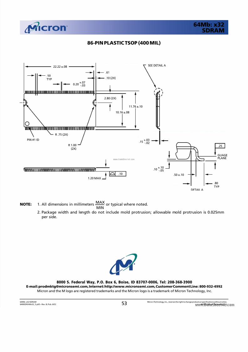
8/11/2019 Mt 48lc2m32b2 - 64mb x32 Sdram
http://slidepdf.com/reader/full/mt-48lc2m32b2-64mb-x32-sdram 53/53
64Mb: x32SDRAM
86-PIN PLASTIC TSOP (400 MIL)
SEE DETAIL A
R 1.00(2X)
R .75 (2X)
.50TYP
.61
10.16 ±.08
.50 ±.10
11.76 ±.10
PIN #1 ID
DETAIL A
22.22 ±.08
0.20 +.07-.03
.15 +.03-.02
.10 +.10-.05
1.20 MAX
.10
.25
GUAGEPLANE
.80TYP
.10 (2X)
2.80 (2X)
NOTE: 1. All dimensions in millimetersMAX
or typical where noted.MIN
2. Package width and length do not include mold protrusion; allowable mold protrusion is 0.025mmper side.