Embed Size (px)
Citation preview
Product
Folder
Order
Now
Technical
Documents
Tools &
Software
Support &Community
ReferenceDesign
An IMPORTANT NOTICE at the end of this data sheet addresses availability, warranty, changes, use in safety-critical applications,intellectual property matters and other important disclaimers. PRODUCTION DATA.
MSP430FR2111, MSP430FR2110, MSP430FR2100, MSP430FR2000SLASE78C –AUGUST 2016–REVISED AUGUST 2018
MSP430FR21xx, MSP430FR2000 Mixed-Signal Microcontrollers
1 Device Overview
1
1.1 Features1
• Embedded Microcontroller– 16-Bit RISC Architecture up to 16 MHz– Wide Supply Voltage Range From 3.6 V Down
to 1.8 V (Minimum Supply Voltage is Restrictedby SVS Levels, See the SVS Specifications)
• Optimized Low-Power Modes (at 3 V)– Active Mode: 120 µA/MHz– Standby
– LPM3.5 With VLO: 1 µA– Real-Time Clock (RTC) Counter (LPM3.5
With 32768-Hz Crystal): 1 µA– Shutdown (LPM4.5): 34 nA Without SVS
• High-Performance Analog– 8-Channel 10-Bit Analog-to-Digital Converter
(ADC)– Integrated Temperature Sensor– Internal 1.5-V Reference– Sample-and-Hold 200 ksps
– Enhanced Comparator (eCOMP)– Integrated 6-Bit DAC as Reference Voltage– Programmable Hysteresis– Configurable High-Power and Low-Power
Modes• Low-Power Ferroelectric RAM (FRAM)
– Up to 3.75KB of Nonvolatile Memory– Built-In Error Correction Code (ECC)– Configurable Write Protection– Unified Memory of Program, Constants, and
Storage– 1015 Write Cycle Endurance– Radiation Resistant and Nonmagnetic
• Intelligent Digital Peripherals– One 16-Bit Timer With Three Capture/Compare
Registers (Timer_B3)– One 16-Bit Counter-Only RTC Counter– 16-Bit Cyclic Redundancy Checker (CRC)
• Enhanced Serial Communications– Enhanced USCI A (eUSCI_A) Supports UART,
IrDA, and SPI
• Clock System (CS)– On-Chip 32-kHz RC Oscillator (REFO)– On-Chip 16-MHz Digitally Controlled Oscillator
(DCO) With Frequency-Locked Loop (FLL)– ±1% Accuracy With On-Chip Reference at
Room Temperature– On-Chip Very-Low-Frequency 10-kHz Oscillator
(VLO)– On-Chip High-Frequency Modulation Oscillator
(MODOSC)– External 32-kHz Crystal Oscillator (LFXT)– Programmable MCLK Prescalar of 1 to 128– SMCLK Derived From MCLK With
Programmable Prescalar of 1, 2, 4, or 8• General Input/Output and Pin Functionality
– 12 I/Os on 16-Pin Package– 8 Interrupt Pins (4 Pins of P1 and 4 Pins of P2)
Can Wake MCU From LPMs– All I/Os are Capacitive Touch I/Os
• Development Tools and Software (Also See Toolsand Software)– Free Professional Development Environments– Development Kits (MSP-TS430PW20,
MSP‑FET430U20, MSP‑EXP430FR2311, andMSP‑EXP430FR4133)
• Family Members (Also See Device Comparison)– MSP430FR2111: 3.75KB of Program FRAM +
1KB of RAM– MSP430FR2110: 2KB of Program FRAM +
1KB of RAM– MSP430FR2100: 1KB of Program FRAM +
512 Bytes of RAM– MSP430FR2000: 0.5KB of Program FRAM +
512 Bytes of RAM• Package Options
– 16-Pin: TSSOP (PW16)– 24-Pin: VQFN (RLL)
• For Complete Module Descriptions, See theMSP430FR4xx and MSP430FR2xx Family User'sGuide
1.2 Applications• Appliance Battery Packs• Smoke and Heat Detectors• Door and Window Sensors• Lighting Sensors
• Power Monitoring• Personal Care Electronics Portable• Health and Fitness Devices
2
MSP430FR2111, MSP430FR2110, MSP430FR2100, MSP430FR2000SLASE78C –AUGUST 2016–REVISED AUGUST 2018 www.ti.com
Submit Documentation FeedbackProduct Folder Links: MSP430FR2111 MSP430FR2110 MSP430FR2100 MSP430FR2000
Device Overview Copyright © 2016–2018, Texas Instruments Incorporated
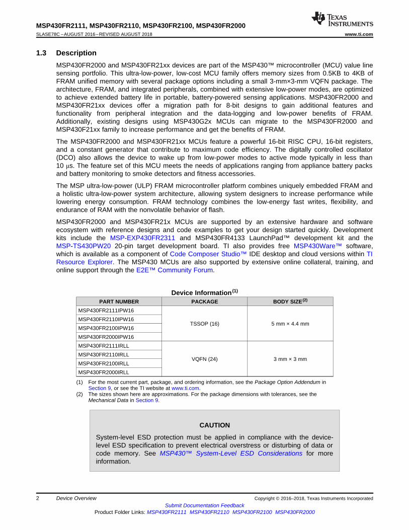
1.3 DescriptionMSP430FR2000 and MSP430FR21xx devices are part of the MSP430™ microcontroller (MCU) value linesensing portfolio. This ultra-low-power, low-cost MCU family offers memory sizes from 0.5KB to 4KB ofFRAM unified memory with several package options including a small 3-mm×3-mm VQFN package. Thearchitecture, FRAM, and integrated peripherals, combined with extensive low-power modes, are optimizedto achieve extended battery life in portable, battery-powered sensing applications. MSP430FR2000 andMSP430FR21xx devices offer a migration path for 8-bit designs to gain additional features andfunctionality from peripheral integration and the data-logging and low-power benefits of FRAM.Additionally, existing designs using MSP430G2x MCUs can migrate to the MSP430FR2000 andMSP430F21xx family to increase performance and get the benefits of FRAM.
The MSP430FR2000 and MSP430FR21xx MCUs feature a powerful 16-bit RISC CPU, 16-bit registers,and a constant generator that contribute to maximum code efficiency. The digitally controlled oscillator(DCO) also allows the device to wake up from low-power modes to active mode typically in less than10 μs. The feature set of this MCU meets the needs of applications ranging from appliance battery packsand battery monitoring to smoke detectors and fitness accessories.
The MSP ultra-low-power (ULP) FRAM microcontroller platform combines uniquely embedded FRAM anda holistic ultra-low-power system architecture, allowing system designers to increase performance whilelowering energy consumption. FRAM technology combines the low-energy fast writes, flexibility, andendurance of RAM with the nonvolatile behavior of flash.
MSP430FR2000 and MSP430FR21x MCUs are supported by an extensive hardware and softwareecosystem with reference designs and code examples to get your design started quickly. Developmentkits include the MSP-EXP430FR2311 and MSP430FR4133 LaunchPad™ development kit and theMSP‑TS430PW20 20-pin target development board. TI also provides free MSP430Ware™ software,which is available as a component of Code Composer Studio™ IDE desktop and cloud versions within TIResource Explorer. The MSP430 MCUs are also supported by extensive online collateral, training, andonline support through the E2E™ Community Forum.
(1) For the most current part, package, and ordering information, see the Package Option Addendum inSection 9, or see the TI website at www.ti.com.
(2) The sizes shown here are approximations. For the package dimensions with tolerances, see theMechanical Data in Section 9.
Device Information (1)
PART NUMBER PACKAGE BODY SIZE (2)
MSP430FR2111IPW16
TSSOP (16) 5 mm × 4.4 mmMSP430FR2110IPW16MSP430FR2100IPW16MSP430FR2000IPW16MSP430FR2111IRLL
VQFN (24) 3 mm × 3 mmMSP430FR2110IRLLMSP430FR2100IRLLMSP430FR2000IRLL
CAUTION
System-level ESD protection must be applied in compliance with the device-level ESD specification to prevent electrical overstress or disturbing of data orcode memory. See MSP430™ System-Level ESD Considerations for moreinformation.
Cap Touch I/O
DVCC
RST/NMI
XIN XOUT P1.x, P2.x
LPM3.5 DomainSBWTDIO
SBWTCK
TDO
TDI/TCLK
TMS
TCK
DVSS
I/O PortsP1 (1×8 I s)
PA (P1, P2)1×12 IOs
OP2 (1×4 I s)O
ADC
8 channels,single ended,
10 bit,200 ksps
(see Note)
ClockSystemControl
LFXT
FRAM
3.75KB2KB1KB
0.5KB
RAM
1KB512 bytes
Watchdog
SYS eUSCI_A0
UART,IrDA, SPI
CRC16
16-bitcyclic
redundancycheck
RTCCounter
16-bitreal-time
clock
JTAG
SBW
TB0
Timer_B3 CC
registers
EEM
MAB
MDB
16-MHz CPUincluding
16 Registers
PowerManagement
Module
eCOMP0
With 6-bitDAC
BAKMEM
32 bytesbackupmemory
Copyright © 2017, Texas Instruments Incorporated
3
MSP430FR2111, MSP430FR2110, MSP430FR2100, MSP430FR2000www.ti.com SLASE78C –AUGUST 2016–REVISED AUGUST 2018
Submit Documentation FeedbackProduct Folder Links: MSP430FR2111 MSP430FR2110 MSP430FR2100 MSP430FR2000
Device OverviewCopyright © 2016–2018, Texas Instruments Incorporated
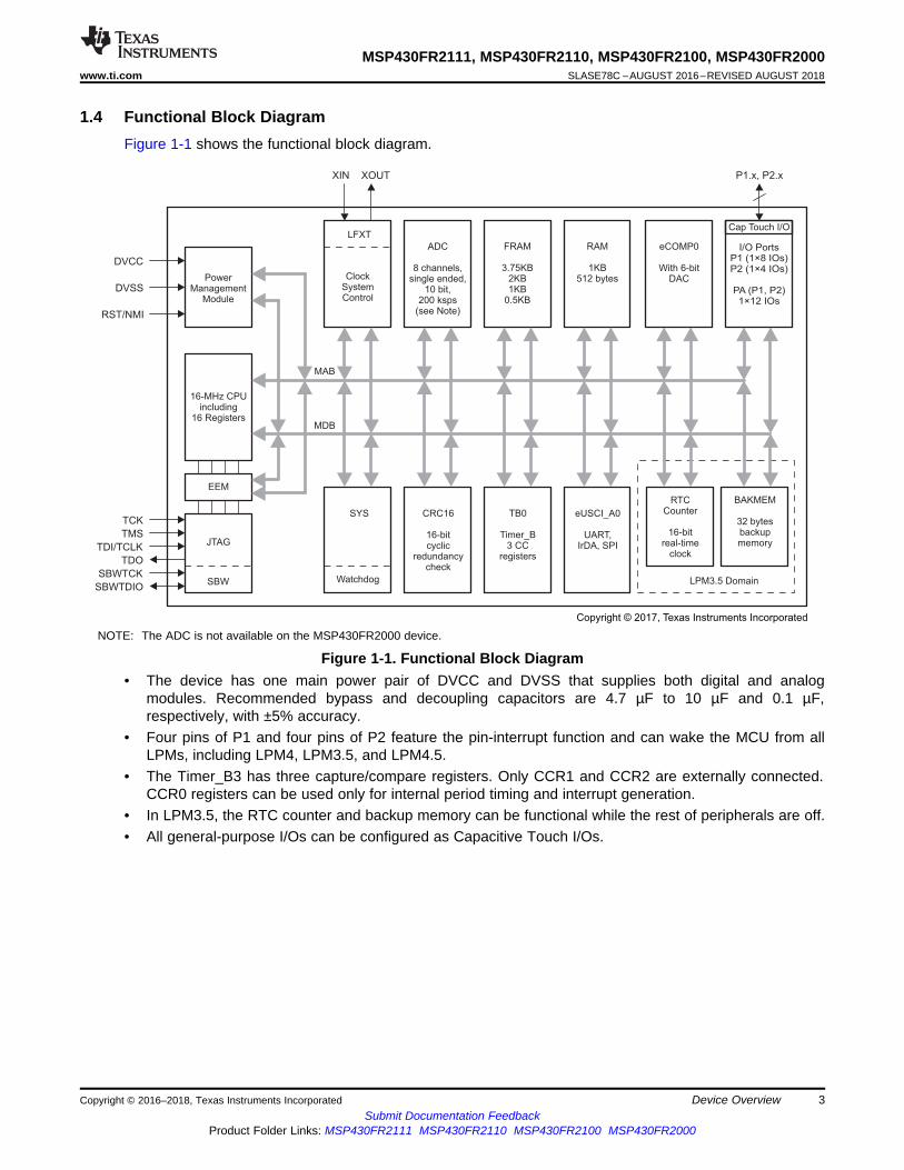
1.4 Functional Block DiagramFigure 1-1 shows the functional block diagram.
NOTE: The ADC is not available on the MSP430FR2000 device.
Figure 1-1. Functional Block Diagram• The device has one main power pair of DVCC and DVSS that supplies both digital and analog
modules. Recommended bypass and decoupling capacitors are 4.7 µF to 10 µF and 0.1 µF,respectively, with ±5% accuracy.
• Four pins of P1 and four pins of P2 feature the pin-interrupt function and can wake the MCU from allLPMs, including LPM4, LPM3.5, and LPM4.5.
• The Timer_B3 has three capture/compare registers. Only CCR1 and CCR2 are externally connected.CCR0 registers can be used only for internal period timing and interrupt generation.
• In LPM3.5, the RTC counter and backup memory can be functional while the rest of peripherals are off.• All general-purpose I/Os can be configured as Capacitive Touch I/Os.
4
MSP430FR2111, MSP430FR2110, MSP430FR2100, MSP430FR2000SLASE78C –AUGUST 2016–REVISED AUGUST 2018 www.ti.com
Submit Documentation FeedbackProduct Folder Links: MSP430FR2111 MSP430FR2110 MSP430FR2100 MSP430FR2000
Table of Contents Copyright © 2016–2018, Texas Instruments Incorporated
Table of Contents1 Device Overview ......................................... 1
1.1 Features .............................................. 11.2 Applications........................................... 11.3 Description............................................ 21.4 Functional Block Diagram ............................ 3
2 Revision History ......................................... 53 Device Comparison ..................................... 6
3.1 Related Products ..................................... 64 Terminal Configuration and Functions.............. 7
4.1 Pin Diagrams ......................................... 74.2 Pin Attributes ......................................... 84.3 Signal Descriptions.................................. 104.4 Pin Multiplexing ..................................... 124.5 Connection of Unused Pins ......................... 124.6 Buffer Type.......................................... 12
5 Specifications ........................................... 135.1 Absolute Maximum Ratings ......................... 135.2 ESD Ratings ........................................ 135.3 Recommended Operating Conditions............... 135.4 Active Mode Supply Current Into VCC Excluding
External Current..................................... 145.5 Active Mode Supply Current Per MHz .............. 145.6 Low-Power Mode LPM0 Supply Currents Into VCC
Excluding External Current.......................... 145.7 Low-Power Mode LPM3, LPM4 Supply Currents
(Into VCC) Excluding External Current .............. 155.8 Typical Characteristics – LPM3 Supply Currents ... 155.9 Low-Power Mode LPMx.5 Supply Currents (Into
VCC) Excluding External Current .................... 165.10 Typical Characteristics – LPMx.5 Supply Currents . 165.11 Typical Characteristics - Current Consumption Per
Module .............................................. 165.12 Thermal Resistance Characteristics ................ 17
5.13 Timing and Switching Characteristics ............... 176 Detailed Description ................................... 35
6.1 Overview ............................................ 356.2 CPU ................................................. 356.3 Operating Modes.................................... 356.4 Interrupt Vector Addresses.......................... 376.5 Memory Organization ............................... 386.6 Bootloader (BSL).................................... 386.7 JTAG Standard Interface............................ 386.8 Spy-Bi-Wire Interface (SBW)........................ 396.9 FRAM................................................ 396.10 Memory Protection .................................. 396.11 Peripherals .......................................... 396.12 Device Descriptors (TLV) ........................... 576.13 Identification ......................................... 58
7 Applications, Implementation, and Layout........ 597.1 Device Connection and Layout Fundamentals...... 597.2 Peripheral- and Interface-Specific Design
Information .......................................... 627.3 Typical Applications ................................. 63
8 Device and Documentation Support ............... 648.1 Getting Started and Next Steps..................... 648.2 Device Nomenclature ............................... 648.3 Tools and Software ................................. 658.4 Documentation Support ............................. 678.5 Related Links........................................ 688.6 Community Resources .............................. 688.7 Trademarks.......................................... 688.8 Electrostatic Discharge Caution..................... 688.9 Glossary ............................................. 68
9 Mechanical, Packaging, and OrderableInformation .............................................. 69
5
MSP430FR2111, MSP430FR2110, MSP430FR2100, MSP430FR2000www.ti.com SLASE78C –AUGUST 2016–REVISED AUGUST 2018
Submit Documentation FeedbackProduct Folder Links: MSP430FR2111 MSP430FR2110 MSP430FR2100 MSP430FR2000
Revision HistoryCopyright © 2016–2018, Texas Instruments Incorporated
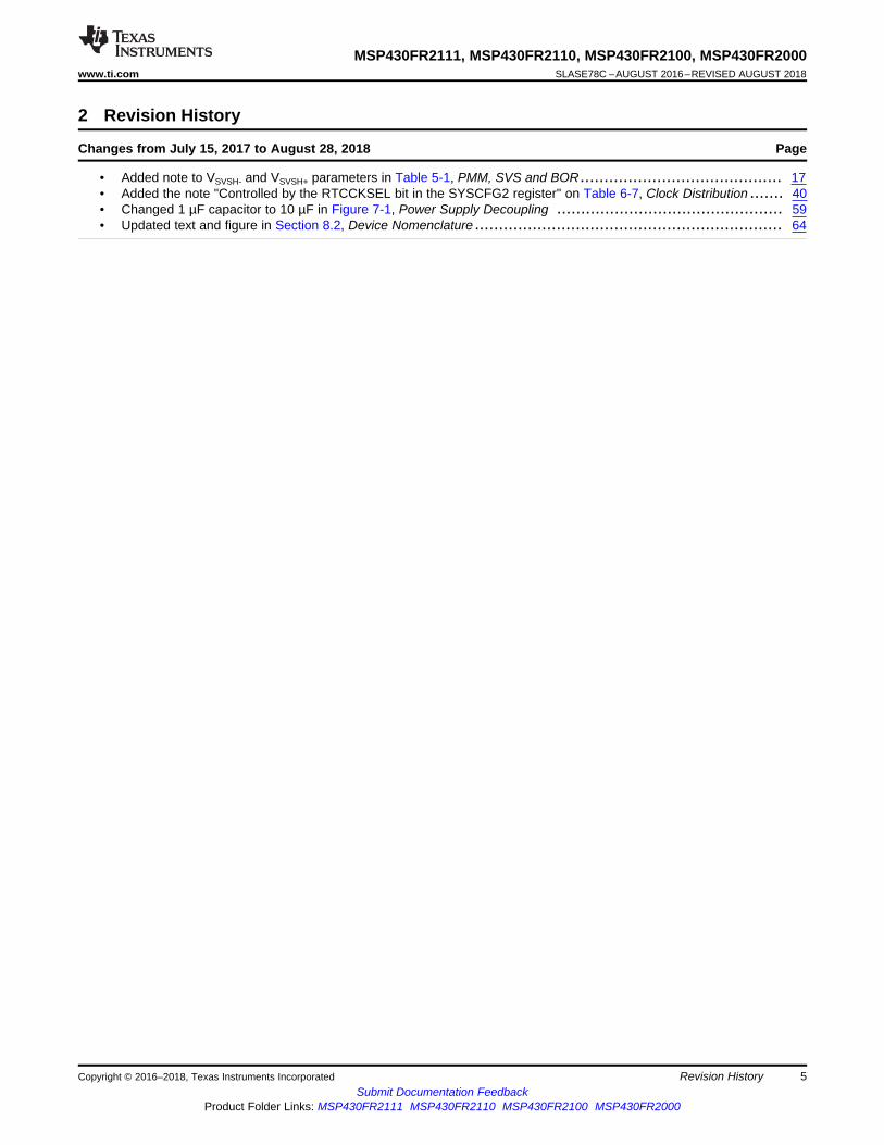
2 Revision History
Changes from July 15, 2017 to August 28, 2018 Page
• Added note to VSVSH- and VSVSH+ parameters in Table 5-1, PMM, SVS and BOR.......................................... 17• Added the note "Controlled by the RTCCKSEL bit in the SYSCFG2 register" on Table 6-7, Clock Distribution ....... 40• Changed 1 µF capacitor to 10 µF in Figure 7-1, Power Supply Decoupling ............................................... 59• Updated text and figure in Section 8.2, Device Nomenclature ................................................................ 64
6
MSP430FR2111, MSP430FR2110, MSP430FR2100, MSP430FR2000SLASE78C –AUGUST 2016–REVISED AUGUST 2018 www.ti.com
Submit Documentation FeedbackProduct Folder Links: MSP430FR2111 MSP430FR2110 MSP430FR2100 MSP430FR2000
Device Comparison Copyright © 2016–2018, Texas Instruments Incorporated
(1) For the most current device, package, and ordering information, see the Package Option Addendum in Section 9, or see the TI websiteat www.ti.com.
(2) Package drawings, standard packing quantities, thermal data, symbolization, and PCB design guidelines are available atwww.ti.com/packaging
(3) A CCR register is a configurable register that provides internal and external capture or compare inputs, or internal and external PWMoutputs.
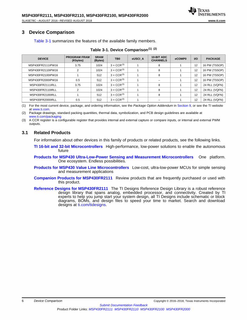
3 Device Comparison
Table 3-1 summarizes the features of the available family members.
Table 3-1. Device Comparison (1) (2)
DEVICE PROGRAM FRAM(Kbytes)
SRAM(Bytes) TB0 eUSCI_A 10-BIT ADC
CHANNELS eCOMP0 I/O PACKAGE
MSP430FR2111IPW16 3.75 1024 3 × CCR (3) 1 8 1 12 16 PW (TSSOP)
MSP430FR2110IPW16 2 1024 3 × CCR (3) 1 8 1 12 16 PW (TSSOP)
MSP430FR2100IPW16 1 512 3 × CCR (3) 1 8 1 12 16 PW (TSSOP)
MSP430FR2000IPW16 0.5 512 3 × CCR (3) 1 – 1 12 16 PW (TSSOP)
MSP430FR2111IRLL 3.75 1024 3 × CCR (3) 1 8 1 12 24 RLL (VQFN)
MSP430FR2110IRLL 2 1024 3 × CCR (3) 1 8 1 12 24 RLL (VQFN)
MSP430FR2100IRLL 1 512 3 × CCR (3) 1 8 1 12 24 RLL (VQFN)
MSP430FR2000IRLL 0.5 512 3 × CCR (3) 1 – 1 12 24 RLL (VQFN)
3.1 Related ProductsFor information about other devices in this family of products or related products, see the following links.TI 16-bit and 32-bit Microcontrollers High-performance, low-power solutions to enable the autonomous
futureProducts for MSP430 Ultra-Low-Power Sensing and Measurement Microcontrollers One platform.
One ecosystem. Endless possibilities.Products for MSP430 Value Line Microcontrollers Low-cost, ultra-low-power MCUs for simple sensing
and measurement applicationsCompanion Products for MSP430FR2111 Review products that are frequently purchased or used with
this product.Reference Designs for MSP430FR2111 The TI Designs Reference Design Library is a robust reference
design library that spans analog, embedded processor, and connectivity. Created by TIexperts to help you jump start your system design, all TI Designs include schematic or blockdiagrams, BOMs, and design files to speed your time to market. Search and downloaddesigns at ti.com/tidesigns.
P2.0
/TB
0.1
/CO
UT
NC
NC
NC
P1.0
/UC
A0S
TE
/SM
CLK
/C0/A
0/V
ere
f+
NC
NC
NC
P2.6
/MC
LK
/XO
UT
P2.1
/TB
0.2
NC
P1.1
/UC
A0C
LK
/AC
LK
/C1/A
1
NC
TEST/SBWTCK
RST/NMI/SBWTDIO
DVCC
DVSS
P2.7/TB0CLK/XIN
P1.5/ /TMS/A5UCA0CLK
P1.4/ /TCK/A4UCA0STE
P1.3/UCA0TXD/UCA0SIMO/C3/A3
P1.2
/UC
A0R
XD
/UC
A0S
OM
I/A
2/V
ere
f-T
B0T
RG
/C2/
P1.6/ /TB0.1/TDI/TCLK/A6UCA0RXD/UCA0SOMI
P1.7/ /TB0.2/TDO/A7UCA0TXD/UCA0SIMO /VREF+
1
2
3
4
5
6
7 8 9 10 11 12
13
14
15
16
17
18
192021222324
1
2
3
4
5
6
7
8 9
10
11
12
13
14
15
16P1.1/UCA0CLK/ACLK/C1/A1
P1.0/UCA0STE/SMCLK/C0/A0/Veref+
TEST/SBWTCK
RST/NMI/SBWTDIO
DVCC
DVSS
P2.7/TB0CLK/XIN
P2.6/MCLK/XOUT
P1.5/ /TMS/A5UCA0CLK
P1.4/ /TCK/A4UCA0STE
P1.3/UCA0TXD/UCA0SIMO/C3/A3
P1.2/UCA0RXD/UCA0SOMI/ A2/Veref-TB0TRG/C2/
P1.6/ /TB0.1/TDI/TCLK/A6UCA0RXD/UCA0SOMI
P2.1/TB0.2
P1.7/ /TB0.2/TDO/A7UCA0TXD/UCA0SIMO /VREF+
P2.0/TB0.1/COUT
7
MSP430FR2111, MSP430FR2110, MSP430FR2100, MSP430FR2000www.ti.com SLASE78C –AUGUST 2016–REVISED AUGUST 2018
Submit Documentation FeedbackProduct Folder Links: MSP430FR2111 MSP430FR2110 MSP430FR2100 MSP430FR2000
Terminal Configuration and FunctionsCopyright © 2016–2018, Texas Instruments Incorporated
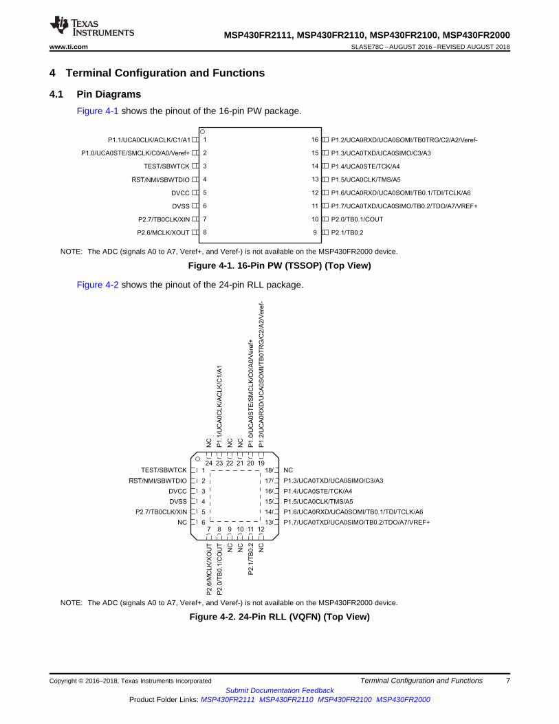
4 Terminal Configuration and Functions
4.1 Pin DiagramsFigure 4-1 shows the pinout of the 16-pin PW package.
NOTE: The ADC (signals A0 to A7, Veref+, and Veref-) is not available on the MSP430FR2000 device.
Figure 4-1. 16-Pin PW (TSSOP) (Top View)
Figure 4-2 shows the pinout of the 24-pin RLL package.
NOTE: The ADC (signals A0 to A7, Veref+, and Veref-) is not available on the MSP430FR2000 device.
Figure 4-2. 24-Pin RLL (VQFN) (Top View)
8
MSP430FR2111, MSP430FR2110, MSP430FR2100, MSP430FR2000SLASE78C –AUGUST 2016–REVISED AUGUST 2018 www.ti.com
Submit Documentation FeedbackProduct Folder Links: MSP430FR2111 MSP430FR2110 MSP430FR2100 MSP430FR2000
Terminal Configuration and Functions Copyright © 2016–2018, Texas Instruments Incorporated
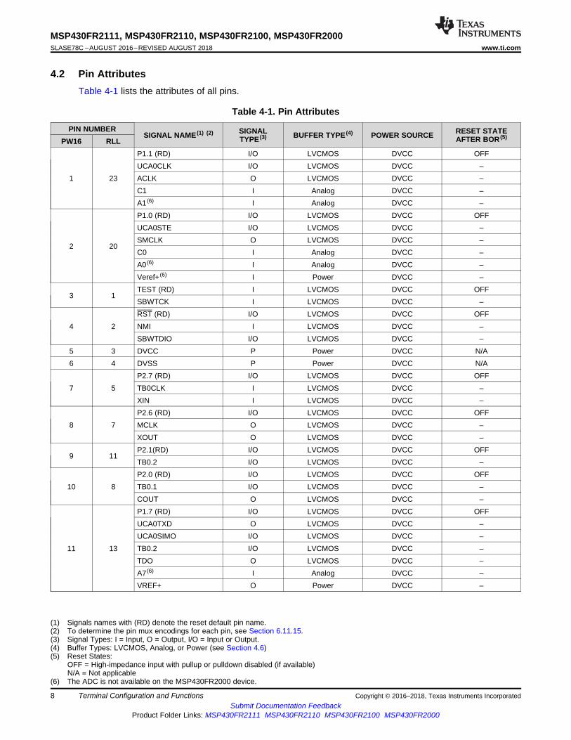
(1) Signals names with (RD) denote the reset default pin name.(2) To determine the pin mux encodings for each pin, see Section 6.11.15.(3) Signal Types: I = Input, O = Output, I/O = Input or Output.(4) Buffer Types: LVCMOS, Analog, or Power (see Section 4.6)(5) Reset States:
OFF = High-impedance input with pullup or pulldown disabled (if available)N/A = Not applicable
(6) The ADC is not available on the MSP430FR2000 device.
4.2 Pin AttributesTable 4-1 lists the attributes of all pins.
Table 4-1. Pin Attributes
PIN NUMBERSIGNAL NAME (1) (2) SIGNAL
TYPE (3) BUFFER TYPE (4) POWER SOURCE RESET STATEAFTER BOR (5)PW16 RLL
1 23
P1.1 (RD) I/O LVCMOS DVCC OFFUCA0CLK I/O LVCMOS DVCC –ACLK O LVCMOS DVCC –C1 I Analog DVCC –A1 (6) I Analog DVCC –
2 20
P1.0 (RD) I/O LVCMOS DVCC OFFUCA0STE I/O LVCMOS DVCC –SMCLK O LVCMOS DVCC –C0 I Analog DVCC –A0 (6) I Analog DVCC –Veref+ (6) I Power DVCC –
3 1TEST (RD) I LVCMOS DVCC OFFSBWTCK I LVCMOS DVCC –
4 2RST (RD) I/O LVCMOS DVCC OFFNMI I LVCMOS DVCC –SBWTDIO I/O LVCMOS DVCC –
5 3 DVCC P Power DVCC N/A6 4 DVSS P Power DVCC N/A
7 5P2.7 (RD) I/O LVCMOS DVCC OFFTB0CLK I LVCMOS DVCC –XIN I LVCMOS DVCC –
8 7P2.6 (RD) I/O LVCMOS DVCC OFFMCLK O LVCMOS DVCC –XOUT O LVCMOS DVCC –
9 11P2.1(RD) I/O LVCMOS DVCC OFFTB0.2 I/O LVCMOS DVCC –
10 8P2.0 (RD) I/O LVCMOS DVCC OFFTB0.1 I/O LVCMOS DVCC –COUT O LVCMOS DVCC –
11 13
P1.7 (RD) I/O LVCMOS DVCC OFFUCA0TXD O LVCMOS DVCC –UCA0SIMO I/O LVCMOS DVCC –TB0.2 I/O LVCMOS DVCC –TDO O LVCMOS DVCC –A7 (6) I Analog DVCC –VREF+ O Power DVCC –
9
MSP430FR2111, MSP430FR2110, MSP430FR2100, MSP430FR2000www.ti.com SLASE78C –AUGUST 2016–REVISED AUGUST 2018
Submit Documentation FeedbackProduct Folder Links: MSP430FR2111 MSP430FR2110 MSP430FR2100 MSP430FR2000
Terminal Configuration and FunctionsCopyright © 2016–2018, Texas Instruments Incorporated
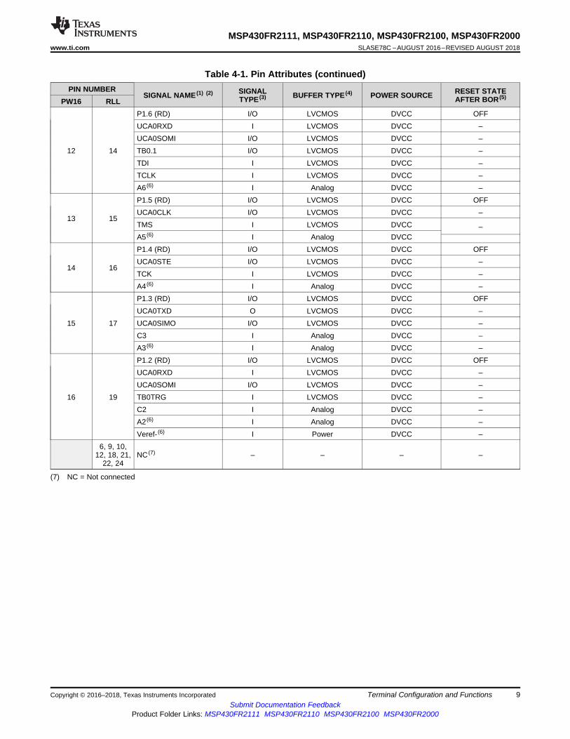
Table 4-1. Pin Attributes (continued)PIN NUMBER
SIGNAL NAME (1) (2) SIGNALTYPE (3) BUFFER TYPE (4) POWER SOURCE RESET STATE
AFTER BOR (5)PW16 RLL
(7) NC = Not connected
12 14
P1.6 (RD) I/O LVCMOS DVCC OFFUCA0RXD I LVCMOS DVCC –UCA0SOMI I/O LVCMOS DVCC –TB0.1 I/O LVCMOS DVCC –TDI I LVCMOS DVCC –TCLK I LVCMOS DVCC –A6 (6) I Analog DVCC –
13 15
P1.5 (RD) I/O LVCMOS DVCC OFFUCA0CLK I/O LVCMOS DVCC –TMS I LVCMOS DVCC –A5 (6) I Analog DVCC
14 16
P1.4 (RD) I/O LVCMOS DVCC OFFUCA0STE I/O LVCMOS DVCC –TCK I LVCMOS DVCC –A4 (6) I Analog DVCC –
15 17
P1.3 (RD) I/O LVCMOS DVCC OFFUCA0TXD O LVCMOS DVCC –UCA0SIMO I/O LVCMOS DVCC –C3 I Analog DVCC –A3 (6) I Analog DVCC –
16 19
P1.2 (RD) I/O LVCMOS DVCC OFFUCA0RXD I LVCMOS DVCC –UCA0SOMI I/O LVCMOS DVCC –TB0TRG I LVCMOS DVCC –C2 I Analog DVCC –A2 (6) I Analog DVCC –Veref- (6) I Power DVCC –
6, 9, 10,12, 18, 21,
22, 24NC (7) – – – –
10
MSP430FR2111, MSP430FR2110, MSP430FR2100, MSP430FR2000SLASE78C –AUGUST 2016–REVISED AUGUST 2018 www.ti.com
Submit Documentation FeedbackProduct Folder Links: MSP430FR2111 MSP430FR2110 MSP430FR2100 MSP430FR2000
Terminal Configuration and Functions Copyright © 2016–2018, Texas Instruments Incorporated
(1) The ADC is not available on the MSP430FR2000 device.
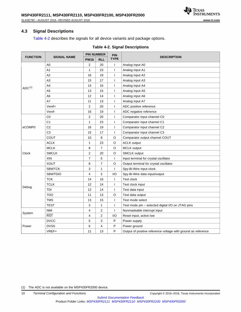
4.3 Signal DescriptionsTable 4-2 describes the signals for all device variants and package options.
Table 4-2. Signal Descriptions
FUNCTION SIGNAL NAMEPIN NUMBER PIN
TYPE DESCRIPTIONPW16 RLL
ADC (1)
A0 2 20 I Analog input A0A1 1 23 I Analog input A1A2 16 19 I Analog input A2A3 15 17 I Analog input A3A4 14 16 I Analog input A4A5 13 15 I Analog input A5A6 12 14 I Analog input A6A7 11 13 I Analog input A7Veref+ 2 20 I ADC positive referenceVeref- 16 19 I ADC negative reference
eCOMP0
C0 2 20 I Comparator input channel C0C1 1 23 I Comparator input channel C1C2 16 19 I Comparator input channel C2C3 15 17 I Comparator input channel C3COUT 10 8 O Comparator output channel COUT
Clock
ACLK 1 23 O ACLK outputMCLK 8 7 O MCLK outputSMCLK 2 20 O SMCLK outputXIN 7 5 I Input terminal for crystal oscillatorXOUT 8 7 O Output terminal for crystal oscillator
Debug
SBWTCK 3 1 I Spy-Bi-Wire input clockSBWTDIO 4 2 I/O Spy-Bi-Wire data input/outputTCK 14 16 I Test clockTCLK 12 14 I Test clock inputTDI 12 14 I Test data inputTDO 11 13 O Test data outputTMS 13 15 I Test mode selectTEST 3 1 I Test mode pin – selected digital I/O on JTAG pins
SystemNMI 4 2 I Nonmaskable interrupt inputRST 4 2 I/O Reset input, active low
PowerDVCC 5 3 P Power supplyDVSS 6 4 P Power groundVREF+ 11 13 P Output of positive reference voltage with ground as reference
11
MSP430FR2111, MSP430FR2110, MSP430FR2100, MSP430FR2000www.ti.com SLASE78C –AUGUST 2016–REVISED AUGUST 2018
Submit Documentation FeedbackProduct Folder Links: MSP430FR2111 MSP430FR2110 MSP430FR2100 MSP430FR2000
Terminal Configuration and FunctionsCopyright © 2016–2018, Texas Instruments Incorporated
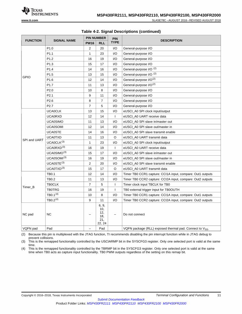
Table 4-2. Signal Descriptions (continued)
FUNCTION SIGNAL NAMEPIN NUMBER PIN
TYPE DESCRIPTIONPW16 RLL
(2) Because this pin is multiplexed with the JTAG function, TI recommends disabling the pin interrupt function while in JTAG debug toprevent collisions.
(3) This is the remapped functionality controlled by the USCIARMP bit in the SYSCFG3 register. Only one selected port is valid at the sametime.
(4) This is the remapped functionality controlled by the TBRMP bit in the SYSCFG3 register. Only one selected port is valid at the sametime when TB0 acts as capture input functionality. TB0 PWM outputs regardless of the setting on this remap bit.
GPIO
P1.0 2 20 I/O General-purpose I/OP1.1 1 23 I/O General-purpose I/OP1.2 16 19 I/O General-purpose I/OP1.3 15 17 I/O General-purpose I/OP1.4 14 16 I/O General-purpose I/O (2)
P1.5 13 15 I/O General-purpose I/O (2)
P1.6 12 14 I/O General-purpose I/O (2)
P1.7 11 13 I/O General-purpose I/O (2)
P2.0 10 8 I/O General-purpose I/OP2.1 9 11 I/O General-purpose I/OP2.6 8 7 I/O General-purpose I/OP2.7 7 5 I/O General-purpose I/O
SPI and UART
UCA0CLK 13 15 I/O eUSCI_A0 SPI clock input/outputUCA0RXD 12 14 I eUSCI_A0 UART receive dataUCA0SIMO 11 13 I/O eUSCI_A0 SPI slave in/master outUCA0SOMI 12 14 I/O eUSCI_A0 SPI slave out/master inUCA0STE 14 16 I/O eUSCI_A0 SPI slave transmit enableUCA0TXD 11 13 O eUSCI_A0 UART transmit dataUCA0CLK (3) 1 23 I/O eUSCI_A0 SPI clock input/outputUCA0RXD (3) 16 19 I eUSCI_A0 UART receive dataUCA0SIMO (3) 15 17 I/O eUSCI_A0 SPI slave in/master outUCA0SOMI (3) 16 19 I/O eUSCI_A0 SPI slave out/master inUCA0STE (3) 2 20 I/O eUSCI_A0 SPI slave transmit enableUCA0TXD (3) 15 17 O eUSCI_A0 UART transmit data
Timer_B
TB0.1 12 14 I/O Timer TB0 CCR1 capture: CCI1A input, compare: Out1 outputsTB0.2 11 13 I/O Timer TB0 CCR2 capture: CCI2A input, compare: Out2 outputsTB0CLK 7 5 I Timer clock input TBCLK for TB0TB0TRG 16 19 I TB0 external trigger input for TB0OUTHTB0.1 (4) 10 8 I/O Timer TB0 CCR1 capture: CCI1A input, compare: Out1 outputsTB0.2 (4) 9 11 I/O Timer TB0 CCR2 capture: CCI2A input, compare: Out2 outputs
NC pad NC –
6, 9,10,12,18,21,
22, 24
– Do not connect
VQFN pad Pad – Pad VQFN package (RLL) exposed thermal pad. Connect to VSS.
12
MSP430FR2111, MSP430FR2110, MSP430FR2100, MSP430FR2000SLASE78C –AUGUST 2016–REVISED AUGUST 2018 www.ti.com
Submit Documentation FeedbackProduct Folder Links: MSP430FR2111 MSP430FR2110 MSP430FR2100 MSP430FR2000
Terminal Configuration and Functions Copyright © 2016–2018, Texas Instruments Incorporated
(1) Any unused pin with a secondary function that is shared with general-purpose I/O should follow the Px.0 to Px.7 unused pin connectionguidelines.
(2) The pulldown capacitor should not exceed 1.1 nF when using devices with Spy-Bi-Wire interface in Spy-Bi-Wire mode with TI tools likeFET interfaces or GANG programmers.
4.4 Pin MultiplexingPin multiplexing for these devices is controlled by both register settings and operating modes (forexample, if the device is in test mode). For details of the settings for each pin and schematics of themultiplexed ports, see Section 6.11.15.
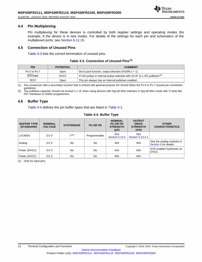
4.5 Connection of Unused PinsTable 4-3 lists the correct termination of unused pins.
Table 4-3. Connection of Unused Pins (1)
PIN POTENTIAL COMMENTPx.0 to Px.7 Open Set to port function, output direction (PxDIR.n = 1)
RST/NMI DVCC 47-kΩ pullup or internal pullup selected with 10-nF (1.1 nF) pulldown (2)
TEST Open This pin always has an internal pulldown enabled.
(1) Only for input pins
4.6 Buffer TypeTable 4-4 defines the pin buffer types that are listed in Table 4-1.
Table 4-4. Buffer Type
BUFFER TYPE(STANDARD)
NOMINALVOLTAGE HYSTERESIS PU OR PD
NOMINALPU OR PD
STRENGTH(µA)
OUTPUTDRIVE
STRENGTH(mA)
OTHERCHARACTERISTICS
LVCMOS 3.0 V Y (1) Programmable SeeSection 5.13.4
SeeSection 5.13.4.1
Analog 3.0 V No No N/A N/A See the analog modules inSection 5 for details.
Power (DVCC) 3.0 V No No N/A N/A SVS enables hysteresis onDVCC.
Power (AVCC) 3.0 V No No N/A N/A
13
MSP430FR2111, MSP430FR2110, MSP430FR2100, MSP430FR2000www.ti.com SLASE78C –AUGUST 2016–REVISED AUGUST 2018
Submit Documentation FeedbackProduct Folder Links: MSP430FR2111 MSP430FR2110 MSP430FR2100 MSP430FR2000
SpecificationsCopyright © 2016–2018, Texas Instruments Incorporated
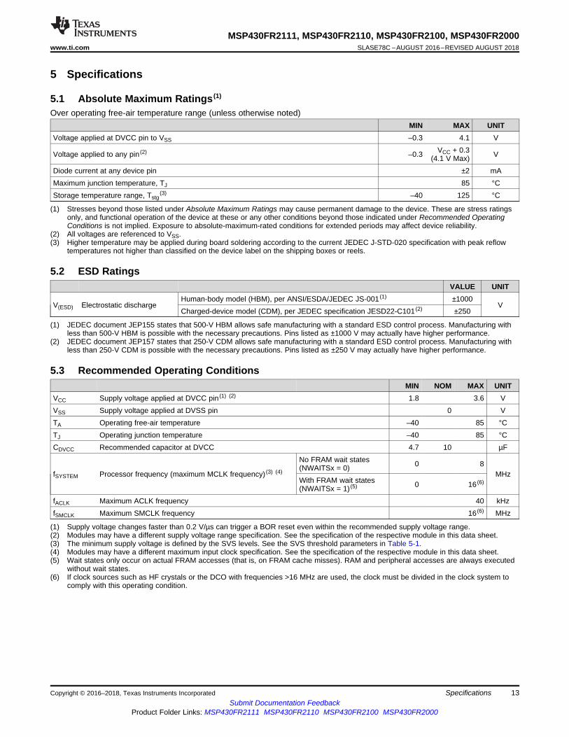
(1) Stresses beyond those listed under Absolute Maximum Ratings may cause permanent damage to the device. These are stress ratingsonly, and functional operation of the device at these or any other conditions beyond those indicated under Recommended OperatingConditions is not implied. Exposure to absolute-maximum-rated conditions for extended periods may affect device reliability.
(2) All voltages are referenced to VSS.(3) Higher temperature may be applied during board soldering according to the current JEDEC J-STD-020 specification with peak reflow
temperatures not higher than classified on the device label on the shipping boxes or reels.
5 Specifications
5.1 Absolute Maximum Ratings (1)
Over operating free-air temperature range (unless otherwise noted)MIN MAX UNIT
Voltage applied at DVCC pin to VSS –0.3 4.1 V
Voltage applied to any pin (2) –0.3 VCC + 0.3(4.1 V Max) V
Diode current at any device pin ±2 mAMaximum junction temperature, TJ 85 °CStorage temperature range, Tstg
(3) –40 125 °C
(1) JEDEC document JEP155 states that 500-V HBM allows safe manufacturing with a standard ESD control process. Manufacturing withless than 500-V HBM is possible with the necessary precautions. Pins listed as ±1000 V may actually have higher performance.
(2) JEDEC document JEP157 states that 250-V CDM allows safe manufacturing with a standard ESD control process. Manufacturing withless than 250-V CDM is possible with the necessary precautions. Pins listed as ±250 V may actually have higher performance.
5.2 ESD RatingsVALUE UNIT
V(ESD) Electrostatic dischargeHuman-body model (HBM), per ANSI/ESDA/JEDEC JS-001 (1) ±1000
VCharged-device model (CDM), per JEDEC specification JESD22-C101 (2) ±250
(1) Supply voltage changes faster than 0.2 V/µs can trigger a BOR reset even within the recommended supply voltage range.(2) Modules may have a different supply voltage range specification. See the specification of the respective module in this data sheet.(3) The minimum supply voltage is defined by the SVS levels. See the SVS threshold parameters in Table 5-1.(4) Modules may have a different maximum input clock specification. See the specification of the respective module in this data sheet.(5) Wait states only occur on actual FRAM accesses (that is, on FRAM cache misses). RAM and peripheral accesses are always executed
without wait states.(6) If clock sources such as HF crystals or the DCO with frequencies >16 MHz are used, the clock must be divided in the clock system to
comply with this operating condition.
5.3 Recommended Operating ConditionsMIN NOM MAX UNIT
VCC Supply voltage applied at DVCC pin (1) (2) 1.8 3.6 VVSS Supply voltage applied at DVSS pin 0 VTA Operating free-air temperature –40 85 °CTJ Operating junction temperature –40 85 °CCDVCC Recommended capacitor at DVCC 4.7 10 µF
fSYSTEM Processor frequency (maximum MCLK frequency) (3) (4)
No FRAM wait states(NWAITSx = 0) 0 8
MHzWith FRAM wait states(NWAITSx = 1) (5) 0 16 (6)
fACLK Maximum ACLK frequency 40 kHzfSMCLK Maximum SMCLK frequency 16 (6) MHz
14
MSP430FR2111, MSP430FR2110, MSP430FR2100, MSP430FR2000SLASE78C –AUGUST 2016–REVISED AUGUST 2018 www.ti.com
Submit Documentation FeedbackProduct Folder Links: MSP430FR2111 MSP430FR2110 MSP430FR2100 MSP430FR2000
Specifications Copyright © 2016–2018, Texas Instruments Incorporated
(1) All inputs are tied to 0 V or to VCC. Outputs do not source or sink any current. Characterized with program executing typical dataprocessing.fACLK = 32768 Hz, fMCLK = fSMCLK = fDCO at specified frequencyProgram and data entirely reside in FRAM. All execution is from FRAM.
(2) Program and data reside entirely in RAM. All execution is from RAM. No access to FRAM.
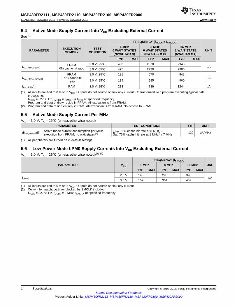
5.4 Active Mode Supply Current Into VCC Excluding External CurrentSee (1)
PARAMETER EXECUTIONMEMORY
TESTCONDITION
FREQUENCY (fMCLK = fSMCLK)
UNIT1 MHz
0 WAIT STATES(NWAITSx = 0)
8 MHz0 WAIT STATES(NWAITSx = 0)
16 MHz1 WAIT STATE(NWAITSx = 1)
TYP MAX TYP MAX TYP MAX
IAM, FRAM (0%)FRAM
0% cache hit ratio3.0 V, 25°C 460 2670 2940
µA3.0 V, 85°C 475 2730 2980
IAM, FRAM (100%)
FRAM100% cache hit
ratio
3.0 V, 25°C 191 570 942µA
3.0 V, 85°C 199 585 960
IAM, RAM(2) RAM 3.0 V, 25°C 213 739 1244 µA
(1) All peripherals are turned on in default settings.
5.5 Active Mode Supply Current Per MHzVCC = 3.0 V, TA = 25°C (unless otherwise noted)
PARAMETER TEST CONDITIONS TYP UNIT
dIAM,FRAM/df Active mode current consumption per MHz,execution from FRAM, no wait states (1)
[(IAM 75% cache hit rate at 8 MHz) –(IAM 75% cache hit rate at 1 MHz)] / 7 MHz 120 µA/MHz
(1) All inputs are tied to 0 V or to VCC. Outputs do not source or sink any current.(2) Current for watchdog timer clocked by SMCLK included.
fACLK = 32768 Hz, fMCLK = 0 MHz, fSMCLK at specified frequency.
5.6 Low-Power Mode LPM0 Supply Currents Into VCC Excluding External CurrentVCC = 3.0 V, TA = 25°C (unless otherwise noted) (1) (2)
PARAMETER VCC
FREQUENCY (fSMCLK)UNIT1 MHz 8 MHz 16 MHz
TYP MAX TYP MAX TYP MAX
ILPM02.0 V 148 295 398
µA3.0 V 157 304 402
0
1
2
3
4
5
6
7
8
9
10
-40
-35
-30
-25
-20
-15
-10 -5 0 5
10
15
20
25
30
35
40
45
50
55
60
65
70
75
80
85
LP
M3
Su
pp
ly C
urr
en
t (µ
A)
Temperature (°C)
15
MSP430FR2111, MSP430FR2110, MSP430FR2100, MSP430FR2000www.ti.com SLASE78C –AUGUST 2016–REVISED AUGUST 2018
Submit Documentation FeedbackProduct Folder Links: MSP430FR2111 MSP430FR2110 MSP430FR2100 MSP430FR2000
SpecificationsCopyright © 2016–2018, Texas Instruments Incorporated
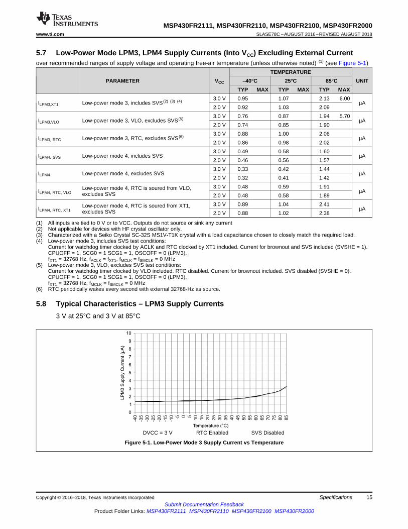
(1) All inputs are tied to 0 V or to VCC. Outputs do not source or sink any current(2) Not applicable for devices with HF crystal oscillator only.(3) Characterized with a Seiko Crystal SC-32S MS1V-T1K crystal with a load capacitance chosen to closely match the required load.(4) Low-power mode 3, includes SVS test conditions:
Current for watchdog timer clocked by ACLK and RTC clocked by XT1 included. Current for brownout and SVS included (SVSHE = 1).CPUOFF = 1, SCG0 = 1 SCG1 = 1, OSCOFF = 0 (LPM3),fXT1 = 32768 Hz, fACLK = fXT1, fMCLK = fSMCLK = 0 MHz
(5) Low-power mode 3, VLO, excludes SVS test conditions:Current for watchdog timer clocked by VLO included. RTC disabled. Current for brownout included. SVS disabled (SVSHE = 0).CPUOFF = 1, SCG0 = 1 SCG1 = 1, OSCOFF = 0 (LPM3),fXT1 = 32768 Hz, fMCLK = fSMCLK = 0 MHz
(6) RTC periodically wakes every second with external 32768-Hz as source.
5.7 Low-Power Mode LPM3, LPM4 Supply Currents (Into VCC) Excluding External Currentover recommended ranges of supply voltage and operating free-air temperature (unless otherwise noted) (1) (see Figure 5-1)
PARAMETER VCC
TEMPERATUREUNIT–40°C 25°C 85°C
TYP MAX TYP MAX TYP MAX
ILPM3,XT1 Low-power mode 3, includes SVS (2) (3) (4) 3.0 V 0.95 1.07 2.13 6.00µA
2.0 V 0.92 1.03 2.09
ILPM3,VLO Low-power mode 3, VLO, excludes SVS (5) 3.0 V 0.76 0.87 1.94 5.70µA
2.0 V 0.74 0.85 1.90
ILPM3, RTC Low-power mode 3, RTC, excludes SVS (6) 3.0 V 0.88 1.00 2.06µA
2.0 V 0.86 0.98 2.02
ILPM4, SVS Low-power mode 4, includes SVS3.0 V 0.49 0.58 1.60
µA2.0 V 0.46 0.56 1.57
ILPM4 Low-power mode 4, excludes SVS3.0 V 0.33 0.42 1.44
µA2.0 V 0.32 0.41 1.42
ILPM4, RTC, VLOLow-power mode 4, RTC is soured from VLO,excludes SVS
3.0 V 0.48 0.59 1.91µA
2.0 V 0.48 0.58 1.89
ILPM4, RTC, XT1Low-power mode 4, RTC is soured from XT1,excludes SVS
3.0 V 0.89 1.04 2.41µA
2.0 V 0.88 1.02 2.38
5.8 Typical Characteristics – LPM3 Supply Currents3 V at 25°C and 3 V at 85°C
DVCC = 3 V RTC Enabled SVS Disabled
Figure 5-1. Low-Power Mode 3 Supply Current vs Temperature
0.00
0.05
0.10
0.15
0.20
0.25
0.30
0.35
0.40
0.45
0.50
-40 -30 -20 -10 0 10 20 30 40 50 60 70 80
LP
M4
.5 S
up
ply
Cu
rre
nt (µ
A)
Temperature (°C)
0.0
0.5
1.0
1.5
2.0
2.5
3.0
-40 -30 -20 -10 0 10 20 30 40 50 60 70 80
LP
M3
.5 S
up
ply
Cu
rre
nt (µ
A)
Temperature (°C)
16
MSP430FR2111, MSP430FR2110, MSP430FR2100, MSP430FR2000SLASE78C –AUGUST 2016–REVISED AUGUST 2018 www.ti.com
Submit Documentation FeedbackProduct Folder Links: MSP430FR2111 MSP430FR2110 MSP430FR2100 MSP430FR2000
Specifications Copyright © 2016–2018, Texas Instruments Incorporated
(1) Not applicable for devices with HF crystal oscillator only.(2) Characterized with a Seiko Crystal SC-32S crystal with a load capacitance chosen to closely match the required load.(3) Low-power mode 3.5, includes SVS test conditions:
Current for RTC clocked by XT1 included. Current for brownout and SVS included (SVSHE = 1). Core regulator disabled.PMMREGOFF = 1, CPUOFF = 1, SCG0 = 1 SCG1 = 1, OSCOFF = 1 (LPMx.5),fXT1 = 32768 Hz, fACLK = fXT1, fMCLK = fSMCLK = 0 MHz
(4) Low-power mode 4.5, includes SVS test conditions:Current for brownout and SVS included (SVSHE = 1). Core regulator disabled.PMMREGOFF = 1, CPUOFF = 1, SCG0 = 1 SCG1 = 1, OSCOFF = 1 (LPMx.5),fXT1 = 0 Hz, fACLK = fMCLK = fSMCLK = 0 MHz
(5) Low-power mode 4.5, excludes SVS test conditions:Current for brownout included. SVS disabled (SVSHE = 0). Core regulator disabled.PMMREGOFF = 1, CPUOFF = 1, SCG0 = 1 SCG1 = 1, OSCOFF = 1 (LPMx.5),fXT1 = 0 Hz, fACLK = fMCLK = fSMCLK = 0 MHz
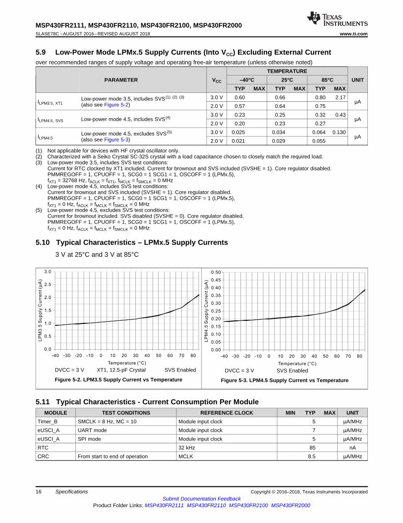
5.9 Low-Power Mode LPMx.5 Supply Currents (Into VCC) Excluding External Currentover recommended ranges of supply voltage and operating free-air temperature (unless otherwise noted)
PARAMETER VCC
TEMPERATUREUNIT–40°C 25°C 85°C
TYP MAX TYP MAX TYP MAX
ILPM3.5, XT1Low-power mode 3.5, includes SVS (1) (2) (3)
(also see Figure 5-2)3.0 V 0.60 0.66 0.80 2.17
µA2.0 V 0.57 0.64 0.75
ILPM4.5, SVS Low-power mode 4.5, includes SVS (4) 3.0 V 0.23 0.25 0.32 0.43µA
2.0 V 0.20 0.23 0.27
ILPM4.5Low-power mode 4.5, excludes SVS (5)
(also see Figure 5-3)3.0 V 0.025 0.034 0.064 0.130
µA2.0 V 0.021 0.029 0.055
5.10 Typical Characteristics – LPMx.5 Supply Currents3 V at 25°C and 3 V at 85°C
DVCC = 3 V XT1, 12.5-pF Crystal SVS Enabled
Figure 5-2. LPM3.5 Supply Current vs TemperatureDVCC = 3 V SVS Enabled
Figure 5-3. LPM4.5 Supply Current vs Temperature
5.11 Typical Characteristics - Current Consumption Per ModuleMODULE TEST CONDITIONS REFERENCE CLOCK MIN TYP MAX UNIT
Timer_B SMCLK = 8 Hz, MC = 10 Module input clock 5 µA/MHzeUSCI_A UART mode Module input clock 7 µA/MHzeUSCI_A SPI mode Module input clock 5 µA/MHzRTC 32 kHz 85 nACRC From start to end of operation MCLK 8.5 µA/MHz
VBOR
VSVS–VSVS+
t
V
Power Cycle Reset SVS Reset BOR Reset
tBOR
17
MSP430FR2111, MSP430FR2110, MSP430FR2100, MSP430FR2000www.ti.com SLASE78C –AUGUST 2016–REVISED AUGUST 2018
Submit Documentation FeedbackProduct Folder Links: MSP430FR2111 MSP430FR2110 MSP430FR2100 MSP430FR2000
SpecificationsCopyright © 2016–2018, Texas Instruments Incorporated
(1) For more information about traditional and new thermal metrics, see Semiconductor and IC Package Thermal Metrics.(2) These values are based on a JEDEC-defined 2S2P system (with the exception of the Theta JC [RθJC] value, which is based on a
JEDEC-defined 1S0P system) and will change based on environment and application. For more information, see these EIA/JEDECstandards:• JESD51-2, Integrated Circuits Thermal Test Method Environmental Conditions - Natural Convection (Still Air)• JESD51-3, Low Effective Thermal Conductivity Test Board for Leaded Surface Mount Packages• JESD51-7, High Effective Thermal Conductivity Test Board for Leaded Surface Mount Packages• JESD51-9, Test Boards for Area Array Surface Mount Package Thermal Measurements
5.12 Thermal Resistance CharacteristicsTHERMAL METRIC (1) (2) VALUE UNIT
RθJA Junction-to-ambient thermal resistance, still airVQFN 24 pin (RLL) 38.7
ºC/WTSSOP 16 pin (PW16) 106.5
RθJC Junction-to-case (top) thermal resistanceVQFN 24 pin (RLL) 39.5
ºC/WTSSOP 16 pin (PW16) 41.2
RθJB Junction-to-board thermal resistanceVQFN 24 pin (RLL) 8.6
ºC/WTSSOP 16 pin (PW16) 51.5
5.13 Timing and Switching Characteristics
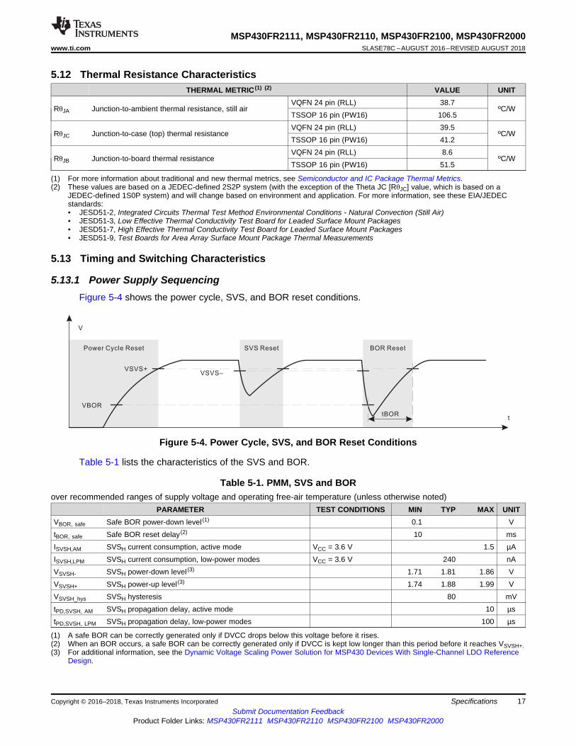
5.13.1 Power Supply SequencingFigure 5-4 shows the power cycle, SVS, and BOR reset conditions.
Figure 5-4. Power Cycle, SVS, and BOR Reset Conditions
Table 5-1 lists the characteristics of the SVS and BOR.
(1) A safe BOR can be correctly generated only if DVCC drops below this voltage before it rises.(2) When an BOR occurs, a safe BOR can be correctly generated only if DVCC is kept low longer than this period before it reaches VSVSH+.(3) For additional information, see the Dynamic Voltage Scaling Power Solution for MSP430 Devices With Single-Channel LDO Reference
Design.
Table 5-1. PMM, SVS and BORover recommended ranges of supply voltage and operating free-air temperature (unless otherwise noted)
PARAMETER TEST CONDITIONS MIN TYP MAX UNITVBOR, safe Safe BOR power-down level (1) 0.1 VtBOR, safe Safe BOR reset delay (2) 10 msISVSH,AM SVSH current consumption, active mode VCC = 3.6 V 1.5 µAISVSH,LPM SVSH current consumption, low-power modes VCC = 3.6 V 240 nAVSVSH- SVSH power-down level (3) 1.71 1.81 1.86 VVSVSH+ SVSH power-up level (3) 1.74 1.88 1.99 VVSVSH_hys SVSH hysteresis 80 mVtPD,SVSH, AM SVSH propagation delay, active mode 10 µstPD,SVSH, LPM SVSH propagation delay, low-power modes 100 µs
18
MSP430FR2111, MSP430FR2110, MSP430FR2100, MSP430FR2000SLASE78C –AUGUST 2016–REVISED AUGUST 2018 www.ti.com
Submit Documentation FeedbackProduct Folder Links: MSP430FR2111 MSP430FR2110 MSP430FR2100 MSP430FR2000
Specifications Copyright © 2016–2018, Texas Instruments Incorporated
5.13.2 Reset TimingTable 5-2 lists the wake-up time characteristics.
(1) The wake-up time is measured from the edge of an external wake-up signal (for example, port interrupt or wake-up event) to the firstexternally observable MCLK clock edge.
(2) The wake-up time is measured from the edge of an external wake-up signal (for example, port interrupt or wake-up event) until the firstinstruction of the user program is executed.
Table 5-2. Wake-up Times From Low-Power Modes and Resetover recommended ranges of supply voltage and operating free-air temperature (unless otherwise noted)
PARAMETER TESTCONDITIONS VCC MIN TYP MAX UNIT
tWAKE-UP FRAM
(Additional) wake-up time to activate the FRAM inAM if previously disabled through the FRAMcontroller or from an LPM if immediate activation isselected for wakeup (1)
3 V 10 µs
tWAKE-UP LPM0 Wake-up time from LPM0 to active mode (1) 3 V 200 +2.5 / fDCO
ns
tWAKE-UP LPM3 Wake-up time from LPM3 to active mode (1) 3 V 10 µstWAKE-UP LPM4 Wake-up time from LPM4 to active mode (2) 3 V 10 µstWAKE-UP LPM3.5 Wake-up time from LPM3.5 to active mode (2) 3 V 350 µs
tWAKE-UP LPM4.5 Wake-up time from LPM4.5 to active mode (2) SVSHE = 13 V
350 µsSVSHE = 0 1 ms
tWAKE-UP-RESETWake-up time from RST or BOR event to activemode (2) 3 V 1 ms
tRESETPulse duration required at RST/NMI pin to accepta reset 2 µs
19
MSP430FR2111, MSP430FR2110, MSP430FR2100, MSP430FR2000www.ti.com SLASE78C –AUGUST 2016–REVISED AUGUST 2018
Submit Documentation FeedbackProduct Folder Links: MSP430FR2111 MSP430FR2110 MSP430FR2100 MSP430FR2000
SpecificationsCopyright © 2016–2018, Texas Instruments Incorporated
5.13.3 Clock SpecificationsTable 5-3 lists the characteristics of the XT1 in low-frequency mode.
(1) To improve EMI on the LFXT oscillator, observe the following guidelines:• Keep the trace between the device and the crystal as short as possible.• Design a good ground plane around the oscillator pins.• Prevent crosstalk from other clock or data lines into oscillator pins XIN and XOUT.• Avoid running PCB traces underneath or adjacent to the XIN and XOUT pins.• Use assembly materials and processes that avoid any parasitic load on the oscillator XIN and XOUT pins.• If conformal coating is used, make sure that it does not induce capacitive or resistive leakage between the oscillator pins.
(2) When LFXTBYPASS is set, LFXT circuits are automatically powered down. The input signal is a digital square wave with parametricsdefined in Table 5-9. Duty cycle requirements are defined by DCLFXT, SW.
(3) Maximum frequency of operation of the entire device cannot be exceeded.(4) Oscillation allowance is based on a safety factor of 5 for recommended crystals. The oscillation allowance is a function of the
LFXTDRIVE settings and the effective load. In general, comparable oscillator allowance can be achieved based on the followingguidelines, but should be evaluated based on the actual crystal selected for the application:• For LFXTDRIVE = 0, CL,eff = 3.7 pF• For LFXTDRIVE = 1, 6 pF ≤ CL,eff ≤ 9 pF• For LFXTDRIVE = 2, 6 pF ≤ CL,eff ≤ 10 pF• For LFXTDRIVE = 3, 6 pF ≤ CL,eff ≤ 12 pF
(5) Includes parasitic bond and package capacitance (approximately 2 pF per pin).(6) Requires external capacitors at both terminals. Values are specified by crystal manufacturers.(7) Includes start-up counter of 1024 clock cycles.(8) Frequencies above the MAX specification do not set the fault flag. Frequencies between the MIN and MAX specifications may set the
flag. A static condition or stuck at fault condition sets the flag.(9) Measured with logic-level input frequency but also applies to operation with crystals.
Table 5-3. XT1 Crystal Oscillator (Low Frequency)over recommended ranges of supply voltage and operating free-air temperature (unless otherwise noted) (1)
PARAMETER TEST CONDITIONS VCC MIN TYP MAX UNIT
fXT1, LFXT1 oscillator crystal, lowfrequency LFXTBYPASS = 0 32768 Hz
DCXT1, LF XT1 oscillator LF duty cycle Measured at MCLK,fLFXT = 32768 Hz 30% 70%
fXT1,SWXT1 oscillator logic-level square-wave input frequency LFXTBYPASS = 1 (2) (3) 32768 Hz
DCXT1, SWLFXT oscillator logic-level square-wave input duty cycle LFXTBYPASS = 1 40% 60%
OALFXTOscillation allowance forLF crystals (4)
LFXTBYPASS = 0, LFXTDRIVE = 3,fLFXT = 32768 Hz, CL,eff = 12.5 pF 200 kΩ
CL,effIntegrated effective loadcapacitance (5) See (6) 1 pF
tSTART,LFXT Start-up time (7)fOSC = 32768 HzLFXTBYPASS = 0, LFXTDRIVE = 3,TA = 25°C, CL,eff = 12.5 pF
1000 ms
fFault,LFXT Oscillator fault frequency (8) XTS = 0 (9) 0 3500 Hz
20
MSP430FR2111, MSP430FR2110, MSP430FR2100, MSP430FR2000SLASE78C –AUGUST 2016–REVISED AUGUST 2018 www.ti.com
Submit Documentation FeedbackProduct Folder Links: MSP430FR2111 MSP430FR2110 MSP430FR2100 MSP430FR2000
Specifications Copyright © 2016–2018, Texas Instruments Incorporated
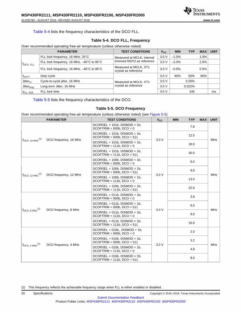
Table 5-4 lists the frequency characteristics of the DCO FLL.
Table 5-4. DCO FLL, FrequencyOver recommended operating free-air temperature (unless otherwise noted)
PARAMETER TEST CONDITIONS VCC MIN TYP MAX UNIT
fDCO, FLL
FLL lock frequency, 16 MHz, 25°C Measured at MCLK, internaltrimmed REFO as reference
3.0 V –1.0% 1.0%FLL lock frequency, 16 MHz, –40°C to 85°C 3.0 V –2.0% 2.0%
FLL lock frequency, 16 MHz, –40°C to 85°C Measured at MCLK, XT1crystal as reference 3.0 V –0.5% 0.5%
fDUTY Duty cycle
Measured at MCLK, XT1crystal as reference
3.0 V 40% 50% 60%Jittercc Cycle-to-cycle jitter, 16 MHz 3.0 V 0.25%Jitterlong Long term Jitter, 16 MHz 3.0 V 0.022%tFLL, lock FLL lock time 3.0 V 245 ms
Table 5-5 lists the frequency characteristics of the DCO.
(1) This frequency reflects the achievable frequency range when FLL is either enabled or disabled.
Table 5-5. DCO FrequencyOver recommended operating free-air temperature (unless otherwise noted) (see Figure 5-5)
PARAMETER TEST CONDITIONS VCC MIN TYP MAX UNIT
fDCO, 16 MHz(1) DCO frequency, 16 MHz
DCORSEL = 101b, DISMOD = 1b,DCOFTRIM = 000b, DCO = 0
3.0 V
7.8
MHz
DCORSEL = 101b, DISMOD = 1b,DCOFTRIM = 000b, DCO = 511 12.5
DCORSEL = 101b, DISMOD = 1b,DCOFTRIM = 111b, DCO = 0 18.0
DCORSEL = 101b, DISMOD = 1b,DCOFTRIM = 111b, DCO = 511 30.0
fDCO, 12 MHz(1) DCO frequency, 12 MHz
DCORSEL = 100b, DISMOD = 1b,DCOFTRIM = 000b, DCO = 0
3.0 V
6.0
MHz
DCORSEL = 100b, DISMOD = 1b,DCOFTRIM = 000b, DCO = 511 9.5
DCORSEL = 100b, DISMOD = 1b,DCOFTRIM = 111b, DCO = 0 13.5
DCORSEL = 100b, DISMOD = 1b,DCOFTRIM = 111b, DCO = 511 22.0
fDCO, 8 MHz(1) DCO frequency, 8 MHz
DCORSEL = 011b, DISMOD = 1b,DCOFTRIM = 000b, DCO = 0
3.0 V
3.8
MHz
DCORSEL = 011b, DISMOD = 1b,DCOFTRIM = 000b, DCO = 511 6.5
DCORSEL = 011b, DISMOD = 1b,DCOFTRIM = 111b, DCO = 0 9.5
DCORSEL = 011b, DISMOD = 1b,DCOFTRIM = 111b, DCO = 511 16.0
fDCO, 4 MHz(1) DCO frequency, 4 MHz
DCORSEL = 010b,, DISMOD = 1b,DCOFTRIM = 000b, DCO = 0
3.0 V
2.0
MHz
DCORSEL = 010b, DISMOD = 1b,DCOFTRIM = 000b, DCO = 511 3.2
DCORSEL = 010b, DISMOD = 1b,DCOFTRIM = 111b, DCO = 0 4.8
DCORSEL = 010b, DISMOD = 1b,DCOFTRIM = 111b, DCO = 511 8.0
0
5
10
15
20
25
30
Fre
quency (
MH
z)
0 1 2 3 4 5DCORSEL
0DCO 511 0 511 0 0 0 0511 511 511 511
DCOFTRIM = 0
DCOFTRIM = 7
DCOFTRIM = 0
DCOFTRIM = 0
DCOFTRIM = 0
DCOFTRIM = 7
DCOFTRIM = 7
DCOFTRIM = 7
DCOFTRIM = 7
DCOFTRIM = 7
DCOFTRIM = 0DCOFTRIM = 0
21
MSP430FR2111, MSP430FR2110, MSP430FR2100, MSP430FR2000www.ti.com SLASE78C –AUGUST 2016–REVISED AUGUST 2018
Submit Documentation FeedbackProduct Folder Links: MSP430FR2111 MSP430FR2110 MSP430FR2100 MSP430FR2000
SpecificationsCopyright © 2016–2018, Texas Instruments Incorporated
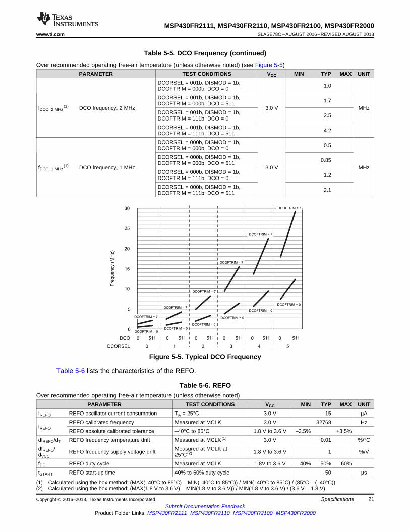
Table 5-5. DCO Frequency (continued)Over recommended operating free-air temperature (unless otherwise noted) (see Figure 5-5)
PARAMETER TEST CONDITIONS VCC MIN TYP MAX UNIT
fDCO, 2 MHz(1) DCO frequency, 2 MHz
DCORSEL = 001b, DISMOD = 1b,DCOFTRIM = 000b, DCO = 0
3.0 V
1.0
MHz
DCORSEL = 001b, DISMOD = 1b,DCOFTRIM = 000b, DCO = 511 1.7
DCORSEL = 001b, DISMOD = 1b,DCOFTRIM = 111b, DCO = 0 2.5
DCORSEL = 001b, DISMOD = 1b,DCOFTRIM = 111b, DCO = 511 4.2
fDCO, 1 MHz(1) DCO frequency, 1 MHz
DCORSEL = 000b, DISMOD = 1b,DCOFTRIM = 000b, DCO = 0
3.0 V
0.5
MHz
DCORSEL = 000b, DISMOD = 1b,DCOFTRIM = 000b, DCO = 511 0.85
DCORSEL = 000b, DISMOD = 1b,DCOFTRIM = 111b, DCO = 0 1.2
DCORSEL = 000b, DISMOD = 1b,DCOFTRIM = 111b, DCO = 511 2.1
Figure 5-5. Typical DCO Frequency
Table 5-6 lists the characteristics of the REFO.
(1) Calculated using the box method: (MAX(–40°C to 85°C) – MIN(–40°C to 85°C)) / MIN(–40°C to 85°C) / (85°C – (–40°C))(2) Calculated using the box method: (MAX(1.8 V to 3.6 V) – MIN(1.8 V to 3.6 V)) / MIN(1.8 V to 3.6 V) / (3.6 V – 1.8 V)
Table 5-6. REFOOver recommended operating free-air temperature (unless otherwise noted)
PARAMETER TEST CONDITIONS VCC MIN TYP MAX UNITIREFO REFO oscillator current consumption TA = 25°C 3.0 V 15 µA
fREFOREFO calibrated frequency Measured at MCLK 3.0 V 32768 HzREFO absolute calibrated tolerance –40°C to 85°C 1.8 V to 3.6 V –3.5% +3.5%
dfREFO/dT REFO frequency temperature drift Measured at MCLK (1) 3.0 V 0.01 %/°CdfREFO/dVCC
REFO frequency supply voltage drift Measured at MCLK at25°C (2) 1.8 V to 3.6 V 1 %/V
fDC REFO duty cycle Measured at MCLK 1.8V to 3.6 V 40% 50% 60%tSTART REFO start-up time 40% to 60% duty cycle 50 µs
22
MSP430FR2111, MSP430FR2110, MSP430FR2100, MSP430FR2000SLASE78C –AUGUST 2016–REVISED AUGUST 2018 www.ti.com
Submit Documentation FeedbackProduct Folder Links: MSP430FR2111 MSP430FR2110 MSP430FR2100 MSP430FR2000
Specifications Copyright © 2016–2018, Texas Instruments Incorporated
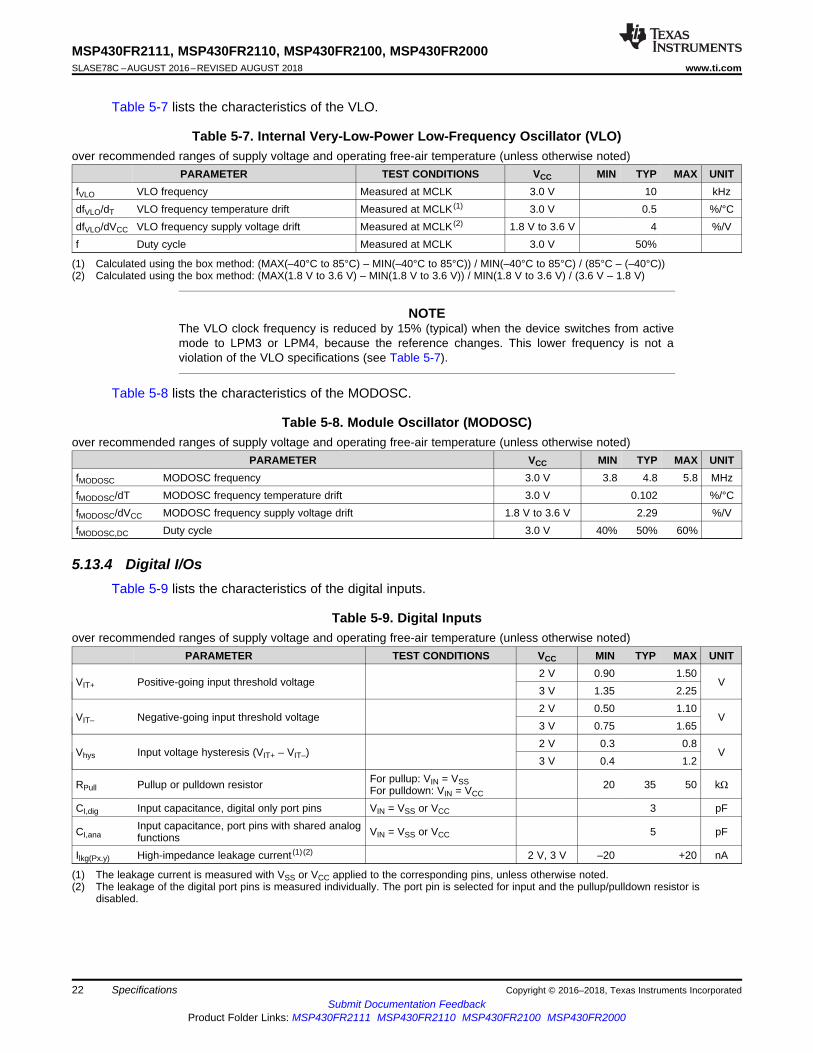
Table 5-7 lists the characteristics of the VLO.
(1) Calculated using the box method: (MAX(–40°C to 85°C) – MIN(–40°C to 85°C)) / MIN(–40°C to 85°C) / (85°C – (–40°C))(2) Calculated using the box method: (MAX(1.8 V to 3.6 V) – MIN(1.8 V to 3.6 V)) / MIN(1.8 V to 3.6 V) / (3.6 V – 1.8 V)
Table 5-7. Internal Very-Low-Power Low-Frequency Oscillator (VLO)over recommended ranges of supply voltage and operating free-air temperature (unless otherwise noted)
PARAMETER TEST CONDITIONS VCC MIN TYP MAX UNITfVLO VLO frequency Measured at MCLK 3.0 V 10 kHzdfVLO/dT VLO frequency temperature drift Measured at MCLK (1) 3.0 V 0.5 %/°CdfVLO/dVCC VLO frequency supply voltage drift Measured at MCLK (2) 1.8 V to 3.6 V 4 %/Vf Duty cycle Measured at MCLK 3.0 V 50%
NOTEThe VLO clock frequency is reduced by 15% (typical) when the device switches from activemode to LPM3 or LPM4, because the reference changes. This lower frequency is not aviolation of the VLO specifications (see Table 5-7).
Table 5-8 lists the characteristics of the MODOSC.
Table 5-8. Module Oscillator (MODOSC)over recommended ranges of supply voltage and operating free-air temperature (unless otherwise noted)
PARAMETER VCC MIN TYP MAX UNITfMODOSC MODOSC frequency 3.0 V 3.8 4.8 5.8 MHzfMODOSC/dT MODOSC frequency temperature drift 3.0 V 0.102 %/°CfMODOSC/dVCC MODOSC frequency supply voltage drift 1.8 V to 3.6 V 2.29 %/VfMODOSC,DC Duty cycle 3.0 V 40% 50% 60%
5.13.4 Digital I/OsTable 5-9 lists the characteristics of the digital inputs.
(1) The leakage current is measured with VSS or VCC applied to the corresponding pins, unless otherwise noted.(2) The leakage of the digital port pins is measured individually. The port pin is selected for input and the pullup/pulldown resistor is
disabled.
Table 5-9. Digital Inputsover recommended ranges of supply voltage and operating free-air temperature (unless otherwise noted)
PARAMETER TEST CONDITIONS VCC MIN TYP MAX UNIT
VIT+ Positive-going input threshold voltage2 V 0.90 1.50
V3 V 1.35 2.25
VIT– Negative-going input threshold voltage2 V 0.50 1.10
V3 V 0.75 1.65
Vhys Input voltage hysteresis (VIT+ – VIT–)2 V 0.3 0.8
V3 V 0.4 1.2
RPull Pullup or pulldown resistor For pullup: VIN = VSSFor pulldown: VIN = VCC
20 35 50 kΩ
CI,dig Input capacitance, digital only port pins VIN = VSS or VCC 3 pF
CI,anaInput capacitance, port pins with shared analogfunctions VIN = VSS or VCC 5 pF
Ilkg(Px.y) High-impedance leakage current (1) (2) 2 V, 3 V –20 +20 nA
Hig
h-L
eve
l O
utp
ut
Cu
rre
nt
(mA
)
-10
-7.5
-5
-2.5
0
0 0.25 0.5 0.75 1 1.25 1.5 1.75 2
High-Level Output Voltage (V)
85°C
25 C°
Hig
h-L
eve
l O
utp
ut C
urr
en
t (m
A)
-25
-20
-15
-10
-5
0
0 0.5 1 1.5 2 2.5 3
High-Level Output Voltage (V)
85°C
25°C
0
5
10
15
20
25
0 0.5 1 1.5 2 2.5 3
Low-Level Output Voltage (V)
85°C
25°C
Lo
w-L
eve
l O
utp
ut
Cu
rre
nt
(mA
)
Lo
w-L
eve
l O
utp
ut C
urr
en
t (m
A)
0
2.5
5
7.5
10
0 0.25 0.5 0.75 1 1.25 1.5 1.75 2
Low-Level Output Voltage (V)
85°C
25°C
23
MSP430FR2111, MSP430FR2110, MSP430FR2100, MSP430FR2000www.ti.com SLASE78C –AUGUST 2016–REVISED AUGUST 2018
Submit Documentation FeedbackProduct Folder Links: MSP430FR2111 MSP430FR2110 MSP430FR2100 MSP430FR2000
SpecificationsCopyright © 2016–2018, Texas Instruments Incorporated
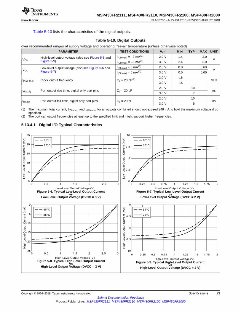
Table 5-10 lists the characteristics of the digital outputs.
(1) The maximum total current, I(OHmax) and I(OLmax), for all outputs combined should not exceed ±48 mA to hold the maximum voltage dropspecified.
(2) The port can output frequencies at least up to the specified limit and might support higher frequencies.
Table 5-10. Digital Outputsover recommended ranges of supply voltage and operating free-air temperature (unless otherwise noted)
PARAMETER TEST CONDITIONS VCC MIN TYP MAX UNIT
VOHHigh-level output voltage (also see Figure 5-8 andFigure 5-9)
I(OHmax) = –3 mA (1) 2.0 V 1.4 2.0V
I(OHmax) = –5 mA (1) 3.0 V 2.4 3.0
VOLLow-level output voltage (also see Figure 5-6 andFigure 5-7)
I(OLmax) = 3 mA (1) 2.0 V 0.0 0.60V
I(OLmax) = 5 mA (1) 3.0 V 0.0 0.60
fPort_CLK Clock output frequency CL = 20 pF (2) 2.0 V 16MHz
3.0 V 16
trise,dig Port output rise time, digital only port pins CL = 20 pF2.0 V 10
ns3.0 V 7
tfall,dig Port output fall time, digital only port pins CL = 20 pF2.0 V 10
ns3.0 V 5
5.13.4.1 Digital I/O Typical Characteristics
Figure 5-6. Typical Low-Level Output Currentvs
Low-Level Output Voltage (DVCC = 3 V)
Figure 5-7. Typical Low-Level Output Currentvs
Low-Level Output Voltage (DVCC = 2 V)
Figure 5-8. Typical High-Level Output Currentvs
High-Level Output Voltage (DVCC = 3 V)Figure 5-9. Typical High-Level Output Current
vsHigh-Level Output Voltage (DVCC = 2 V)
24
MSP430FR2111, MSP430FR2110, MSP430FR2100, MSP430FR2000SLASE78C –AUGUST 2016–REVISED AUGUST 2018 www.ti.com
Submit Documentation FeedbackProduct Folder Links: MSP430FR2111 MSP430FR2110 MSP430FR2100 MSP430FR2000
Specifications Copyright © 2016–2018, Texas Instruments Incorporated
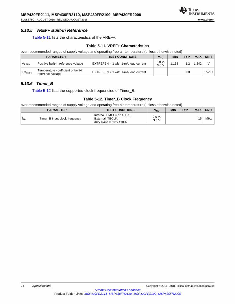
5.13.5 VREF+ Built-in ReferenceTable 5-11 lists the characteristics of the VREF+.
Table 5-11. VREF+ Characteristicsover recommended ranges of supply voltage and operating free-air temperature (unless otherwise noted)
PARAMETER TEST CONDITIONS VCC MIN TYP MAX UNIT
VREF+ Positive built-in reference voltage EXTREFEN = 1 with 1-mA load current 2.0 V,3.0 V 1.158 1.2 1.242 V
TCREF+Temperature coefficient of built-inreference voltage EXTREFEN = 1 with 1-mA load current 30 µV/°C
5.13.6 Timer_BTable 5-12 lists the supported clock frequencies of Timer_B.
Table 5-12. Timer_B Clock Frequencyover recommended ranges of supply voltage and operating free-air temperature (unless otherwise noted)
PARAMETER TEST CONDITIONS VCC MIN TYP MAX UNIT
fTB Timer_B input clock frequencyInternal: SMCLK or ACLK,External: TBCLK,duty cycle = 50% ±10%
2.0 V,3.0 V 16 MHz
25
MSP430FR2111, MSP430FR2110, MSP430FR2100, MSP430FR2000www.ti.com SLASE78C –AUGUST 2016–REVISED AUGUST 2018
Submit Documentation FeedbackProduct Folder Links: MSP430FR2111 MSP430FR2110 MSP430FR2100 MSP430FR2000
SpecificationsCopyright © 2016–2018, Texas Instruments Incorporated
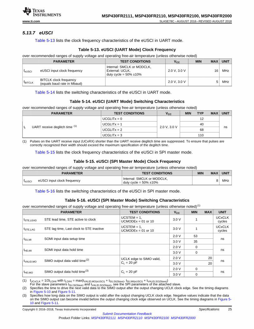
5.13.7 eUSCITable 5-13 lists the clock frequency characteristics of the eUSCI in UART mode.
Table 5-13. eUSCI (UART Mode) Clock Frequencyover recommended ranges of supply voltage and operating free-air temperature (unless otherwise noted)
PARAMETER TEST CONDITIONS VCC MIN MAX UNIT
feUSCI eUSCI input clock frequencyInternal: SMCLK or MODCLK,External: UCLK,duty cycle = 50% ±10%
2.0 V, 3.0 V 16 MHz
fBITCLKBITCLK clock frequency(equals baud rate in Mbaud) 2.0 V, 3.0 V 5 MHz
Table 5-14 lists the switching characteristics of the eUSCI in UART mode.
(1) Pulses on the UART receive input (UCxRX) shorter than the UART receive deglitch time are suppressed. To ensure that pulses arecorrectly recognized their width should exceed the maximum specification of the deglitch time.
Table 5-14. eUSCI (UART Mode) Switching Characteristicsover recommended ranges of supply voltage and operating free-air temperature (unless otherwise noted)
PARAMETER TEST CONDITIONS VCC MIN TYP MAX UNIT
tt UART receive deglitch time (1)
UCGLITx = 0
2.0 V, 3.0 V
12
nsUCGLITx = 1 40UCGLITx = 2 68UCGLITx = 3 110
Table 5-15 lists the clock frequency characteristics of the eUSCI in SPI master mode.
Table 5-15. eUSCI (SPI Master Mode) Clock Frequencyover recommended ranges of supply voltage and operating free-air temperature (unless otherwise noted)
PARAMETER TEST CONDITIONS MIN MAX UNIT
feUSCI eUSCI input clock frequency Internal: SMCLK or MODCLK,duty cycle = 50% ±10% 8 MHz
Table 5-16 lists the switching characteristics of the eUSCI in SPI master mode.
(1) fUCxCLK = 1/2tLO/HI with tLO/HI = max(tVALID,MO(eUSCI) + tSU,SI(Slave), tSU,MI(eUSCI) + tVALID,SO(Slave))For the slave parameters tSU,SI(Slave) and tVALID,SO(Slave), see the SPI parameters of the attached slave.
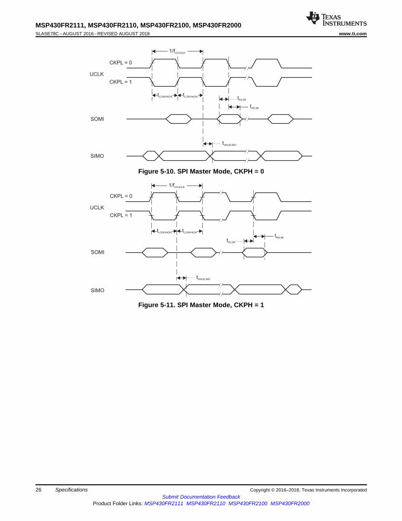
(2) Specifies the time to drive the next valid data to the SIMO output after the output changing UCLK clock edge. See the timing diagramsin Figure 5-10 and Figure 5-11.
(3) Specifies how long data on the SIMO output is valid after the output changing UCLK clock edge. Negative values indicate that the dataon the SIMO output can become invalid before the output changing clock edge observed on UCLK. See the timing diagrams in Figure 5-10 and Figure 5-11.
Table 5-16. eUSCI (SPI Master Mode) Switching Characteristicsover recommended ranges of supply voltage and operating free-air temperature (unless otherwise noted) (1)
PARAMETER TEST CONDITIONS VCC MIN MAX UNIT
tSTE,LEAD STE lead time, STE active to clock UCSTEM = 1,UCMODEx = 01 or 10 3.0 V 1 UCxCLK
cycles
tSTE,LAG STE lag time, Last clock to STE inactive UCSTEM = 1,UCMODEx = 01 or 10 3.0 V 1 UCxCLK
cycles
tSU,MI SOMI input data setup time2.0 V 53
ns3.0 V 35
tHD,MI SOMI input data hold time2.0 V 0
ns3.0 V 0
tVALID,MO SIMO output data valid time (2) UCLK edge to SIMO valid,CL = 20 pF
2.0 V 20ns
3.0 V 20
tHD,MO SIMO output data hold time (3) CL = 20 pF2.0 V 0
ns3.0 V 0
tSU,MI
tHD,MI
UCLK
SOMI
SIMO
tVALID,MO
CKPL = 0
CKPL = 1
tLOW/HIGH tLOW/HIGH
1/fUCxCLK
tSU,MI
tHD,MI
UCLK
SOMI
SIMO
tVALID,MO
CKPL = 0
CKPL = 1
tLOW/HIGH tLOW/HIGH
1/fUCxCLK
26
MSP430FR2111, MSP430FR2110, MSP430FR2100, MSP430FR2000SLASE78C –AUGUST 2016–REVISED AUGUST 2018 www.ti.com
Submit Documentation FeedbackProduct Folder Links: MSP430FR2111 MSP430FR2110 MSP430FR2100 MSP430FR2000
Specifications Copyright © 2016–2018, Texas Instruments Incorporated
Figure 5-10. SPI Master Mode, CKPH = 0
Figure 5-11. SPI Master Mode, CKPH = 1
27
MSP430FR2111, MSP430FR2110, MSP430FR2100, MSP430FR2000www.ti.com SLASE78C –AUGUST 2016–REVISED AUGUST 2018
Submit Documentation FeedbackProduct Folder Links: MSP430FR2111 MSP430FR2110 MSP430FR2100 MSP430FR2000
SpecificationsCopyright © 2016–2018, Texas Instruments Incorporated
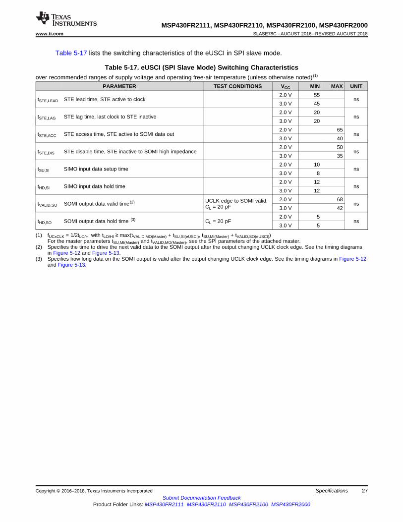
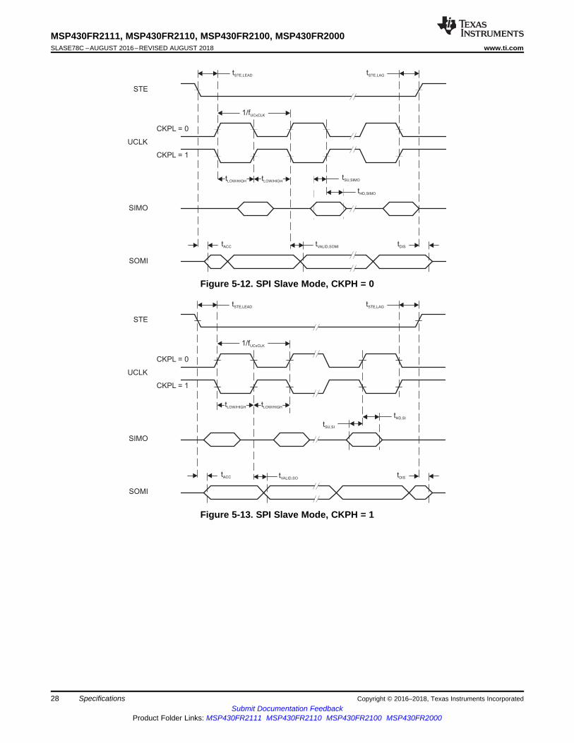
Table 5-17 lists the switching characteristics of the eUSCI in SPI slave mode.
(1) fUCxCLK = 1/2tLO/HI with tLO/HI ≥ max(tVALID,MO(Master) + tSU,SI(eUSCI), tSU,MI(Master) + tVALID,SO(eUSCI))For the master parameters tSU,MI(Master) and tVALID,MO(Master), see the SPI parameters of the attached master.
(2) Specifies the time to drive the next valid data to the SOMI output after the output changing UCLK clock edge. See the timing diagramsin Figure 5-12 and Figure 5-13.
(3) Specifies how long data on the SOMI output is valid after the output changing UCLK clock edge. See the timing diagrams in Figure 5-12and Figure 5-13.
Table 5-17. eUSCI (SPI Slave Mode) Switching Characteristicsover recommended ranges of supply voltage and operating free-air temperature (unless otherwise noted) (1)
PARAMETER TEST CONDITIONS VCC MIN MAX UNIT
tSTE,LEAD STE lead time, STE active to clock2.0 V 55
ns3.0 V 45
tSTE,LAG STE lag time, last clock to STE inactive2.0 V 20
ns3.0 V 20
tSTE,ACC STE access time, STE active to SOMI data out2.0 V 65
ns3.0 V 40
tSTE,DIS STE disable time, STE inactive to SOMI high impedance2.0 V 50
ns3.0 V 35
tSU,SI SIMO input data setup time2.0 V 10
ns3.0 V 8
tHD,SI SIMO input data hold time2.0 V 12
ns3.0 V 12
tVALID,SO SOMI output data valid time (2) UCLK edge to SOMI valid,CL = 20 pF
2.0 V 68ns
3.0 V 42
tHD,SO SOMI output data hold time (3) CL = 20 pF2.0 V 5
ns3.0 V 5
STE
UCLK
CKPL = 0
CKPL = 1
SOMI
SIMO
tSU,SI
tHD,SI
tVALID,SO
tSTE,LEAD
tLOW/HIGH
1/fUCxCLK
tLOW/HIGH
tSTE,LAG
tDIStACC
STE
UCLK
CKPL = 0
CKPL = 1
SOMI
SIMO
tSU,SIMO
tHD,SIMO
tVALID,SOMI
tSTE,LEAD
tLOW/HIGH
1/fUCxCLK
tLOW/HIGH
tSTE,LAG
tDIStACC
28
MSP430FR2111, MSP430FR2110, MSP430FR2100, MSP430FR2000SLASE78C –AUGUST 2016–REVISED AUGUST 2018 www.ti.com
Submit Documentation FeedbackProduct Folder Links: MSP430FR2111 MSP430FR2110 MSP430FR2100 MSP430FR2000
Specifications Copyright © 2016–2018, Texas Instruments Incorporated
Figure 5-12. SPI Slave Mode, CKPH = 0
Figure 5-13. SPI Slave Mode, CKPH = 1
29
MSP430FR2111, MSP430FR2110, MSP430FR2100, MSP430FR2000www.ti.com SLASE78C –AUGUST 2016–REVISED AUGUST 2018
Submit Documentation FeedbackProduct Folder Links: MSP430FR2111 MSP430FR2110 MSP430FR2100 MSP430FR2000
SpecificationsCopyright © 2016–2018, Texas Instruments Incorporated
5.13.8 ADC
NOTEThe ADC is not available on the MSP430FR2000 device.
Table 5-18 lists the input conditions of the ADC.
Table 5-18. ADC, Power Supply and Input Range ConditionsOver operating free-air temperature range (unless otherwise noted)
PARAMETER TEST CONDITIONS VCC MIN TYP MAX UNITDVCC ADC supply voltage 2.0 3.6 VV(Ax) Analog input voltage range All ADC pins 0 DVCC V
IADC
Operating supply current into DVCCterminal, reference current not included,repeat-single-channel mode
fADCCLK = 5 MHz, ADCON = 1,REFON = 0, SHT0 = 0, SHT1 = 0,ADCDIV = 0, ADCCONSEQx = 10b
2 V 185µA
3 V 207
CI Input capacitanceOnly one terminal Ax can be selected atone time from the pad to the ADC capacitorarray, including wiring and pad
2.2 V 2.5 3.5 pF
RI Input MUX ON resistance DVCC = 2 V, 0 V = VAx = DVCC 2 kΩ
Table 5-19 lists the timing parameters of the ADC.
Table 5-19. ADC, 10-Bit Timing ParametersOver operating free-air temperature range (unless otherwise noted)
PARAMETER TEST CONDITIONS VCC MIN TYP MAX UNIT
fADCCLKFor specified performance of ADC linearityparameters
2 V to3.6 V 0.45 5 5.5 MHz
fADCOSCInternal ADC oscillator(MODOSC) ADCDIV = 0, fADCCLK = fADCOSC
2 V to3.6 V 3.8 4.8 5.8 MHz
tCONVERT Conversion timeREFON = 0, Internal oscillator,10 ADCCLK cycles, 10-bit mode,fADCOSC = 4.5 MHz to 5.5 MHz
2 V to3.6 V 2.18 2.67 µs
tADCONTurnon settling time ofthe ADC
The error in a conversion started after tADCON is lessthan ±0.5 LSB.Reference and input signal are already settled.
100 ns
tSample Sampling timeRS = 1000 Ω, RI = 36000 Ω, CI = 3.5 pF.Approximately 8 Tau (t) are required for an error ofless than ±0.5 LSB.
2 V 1.5µs
3 V 2.0
30
MSP430FR2111, MSP430FR2110, MSP430FR2100, MSP430FR2000SLASE78C –AUGUST 2016–REVISED AUGUST 2018 www.ti.com
Submit Documentation FeedbackProduct Folder Links: MSP430FR2111 MSP430FR2110 MSP430FR2100 MSP430FR2000
Specifications Copyright © 2016–2018, Texas Instruments Incorporated
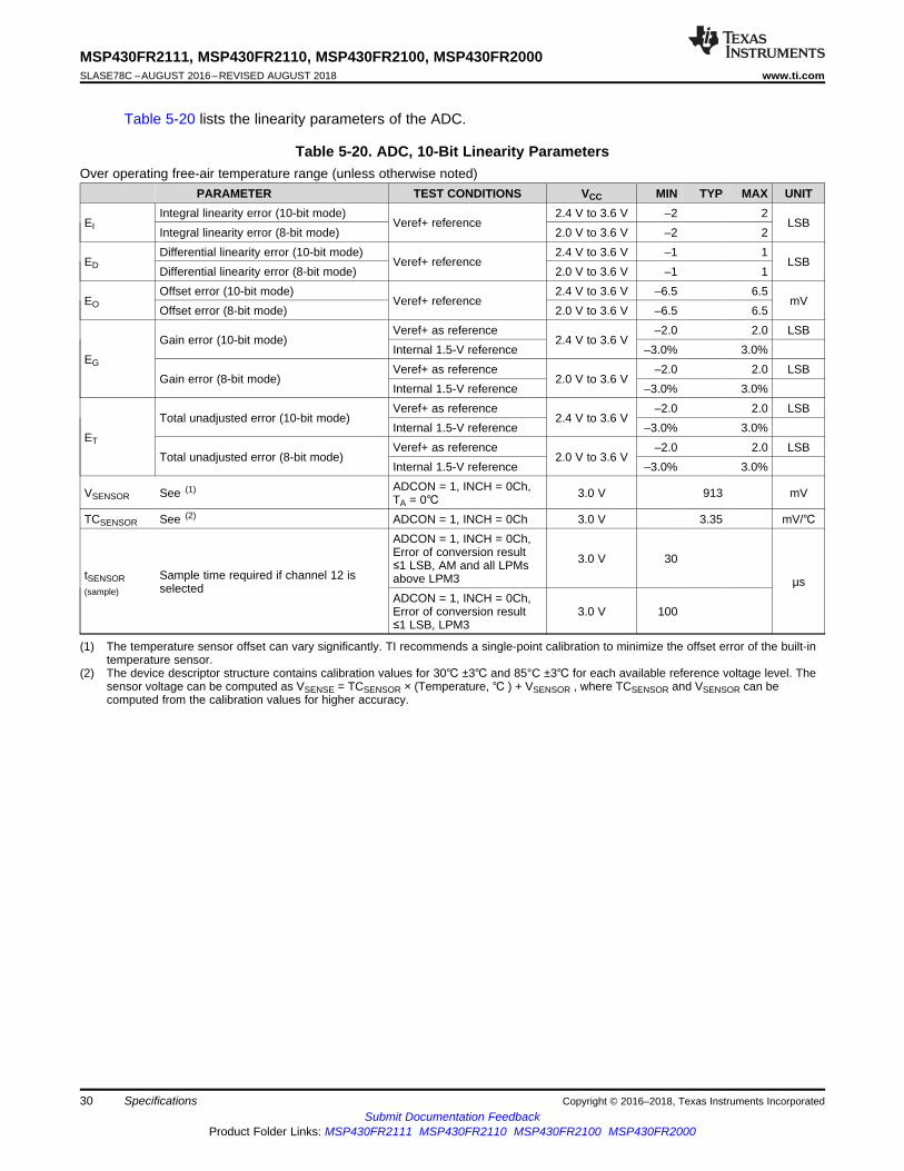
Table 5-20 lists the linearity parameters of the ADC.
(1) The temperature sensor offset can vary significantly. TI recommends a single-point calibration to minimize the offset error of the built-intemperature sensor.
(2) The device descriptor structure contains calibration values for 30 ±3 and 85°C ±3 for each available reference voltage level. Thesensor voltage can be computed as VSENSE = TCSENSOR × (Temperature, ) + VSENSOR , where TCSENSOR and VSENSOR can becomputed from the calibration values for higher accuracy.
Table 5-20. ADC, 10-Bit Linearity ParametersOver operating free-air temperature range (unless otherwise noted)
PARAMETER TEST CONDITIONS VCC MIN TYP MAX UNIT
EIIntegral linearity error (10-bit mode)
Veref+ reference2.4 V to 3.6 V –2 2
LSBIntegral linearity error (8-bit mode) 2.0 V to 3.6 V –2 2
EDDifferential linearity error (10-bit mode)
Veref+ reference2.4 V to 3.6 V –1 1
LSBDifferential linearity error (8-bit mode) 2.0 V to 3.6 V –1 1
EOOffset error (10-bit mode)
Veref+ reference2.4 V to 3.6 V –6.5 6.5
mVOffset error (8-bit mode) 2.0 V to 3.6 V –6.5 6.5
EG
Gain error (10-bit mode)Veref+ as reference
2.4 V to 3.6 V–2.0 2.0 LSB
Internal 1.5-V reference –3.0% 3.0%
Gain error (8-bit mode)Veref+ as reference
2.0 V to 3.6 V–2.0 2.0 LSB
Internal 1.5-V reference –3.0% 3.0%
ET
Total unadjusted error (10-bit mode)Veref+ as reference
2.4 V to 3.6 V–2.0 2.0 LSB
Internal 1.5-V reference –3.0% 3.0%
Total unadjusted error (8-bit mode)Veref+ as reference
2.0 V to 3.6 V–2.0 2.0 LSB
Internal 1.5-V reference –3.0% 3.0%
VSENSOR See (1) ADCON = 1, INCH = 0Ch,TA = 0 3.0 V 913 mV
TCSENSOR See (2) ADCON = 1, INCH = 0Ch 3.0 V 3.35 mV/
tSENSOR(sample)
Sample time required if channel 12 isselected
ADCON = 1, INCH = 0Ch,Error of conversion result≤1 LSB, AM and all LPMsabove LPM3
3.0 V 30
µsADCON = 1, INCH = 0Ch,Error of conversion result≤1 LSB, LPM3
3.0 V 100

31
MSP430FR2111, MSP430FR2110, MSP430FR2100, MSP430FR2000www.ti.com SLASE78C –AUGUST 2016–REVISED AUGUST 2018
Submit Documentation FeedbackProduct Folder Links: MSP430FR2111 MSP430FR2110 MSP430FR2100 MSP430FR2000
SpecificationsCopyright © 2016–2018, Texas Instruments Incorporated
5.13.9 Enhanced Comparator (eCOMP)Table 5-21 lists the characteristics of the eCOMP.
(1) For the eCOMP CIN model, see Figure 5-14.(2) This is measured over the input offset.
Table 5-21. eCOMPover recommended ranges of supply voltage and operating free-air temperature (unless otherwise noted)
PARAMETER TEST CONDITIONS VCC MIN TYP MAX UNITVCC Supply voltage 2.0 3.6 V
VICCommon-mode inputrange 0 VCC V
VHYS DC input hysteresis
CPEN = 1, CPHSEL = 00
2.0 V to 3.6 V
0
mVCPEN = 1, CPHSEL = 01 10CPEN = 1, CPHSEL = 10 20CPEN = 1, CPHSEL = 11 30
VOFFSET Input offset voltageCPEN = 1, CPMSEL = 0, CPHSEL = 00
2.0 V to 3.6 V–40 ±5 –40
mVCPEN = 1, CPMSEL = 1, CPHSEL = 00 ±10
ICOMP
Quiescent current drawfrom VCC, onlycomparator
VIC = VCC/2, CPEN = 1, CPMSEL = 02.0 V to 3.6 V
22 35µA
VIC = VCC/2, CPEN = 1, CPMSEL = 1 1.3 3.5
IDACQuiescent current drawfrom VCC, only DAC CPDACREFS = 0, CPEN = 0 2.0 V to 3.6 V 0.5 µA
CINInput channelcapacitance (1) 2.0 V to 3.6 V 1 pF
RINInput channel seriesresistance
On (switch closed)2.0 V to 3.6 V
10 20 kΩOff (switch open) 50 MΩ
tPDPropagation delay,response time
CPMSEL = 0, CPFLT = 0,Overdrive = 20 mV (2)
2.0 V to 3.6 V1
µsCPMSEL = 1, CPFLT = 0,Overdrive = 20 mV (2) 2.4
tEN_CPComparator enabletime
CPEN = 0→1, CPMSEL = 0,V+ and V- from pads, Overdrive = 20 mV (2)
2.0 V to 3.6 V9.3
µsCPEN = 0→1, CPMSEL = 1,V+ and V- from pads, Overdrive = 20 mV (2) 12
tEN_CP_DAC
Comparator withreference DAC enabletime
CPEN = 0→1, CPDACEN=0→1,CPMSEL = 0, CPDACREFS = 1,CPDACBUF1 = 0F, Overdrive = 20 mV (2)
2.0 V to 3.6 V
9.3
µsCPEN = 0→1, CPDACEN=0→1,CPMSEL = 1, CPDACREFS = 1,CPDACBUF1 = 0F, Overdrive = 20 mV (2)
113
tFDLYPropagation delay withanalog filter active
CPMSEL = 0, CPFLTDY = 00,Overdrive = 20 mV, (2)
CPFLT = 1
2.0 V to 3.6 V
0.7
µs
CPMSEL = 0, CPFLTDY = 01,Overdrive = 20 mV, (2)
CPFLT = 11.1
CPMSEL = 0, CPFLTDY = 10,Overdrive = 20 mV, (2) CPFLT = 1 1.9
CPMSEL = 0, CPFLTDY = 11,Overdrive = 20 mV, (2) CPFLT = 1 3.7
VCP_DACReference voltage forbuilt-in 6-bit DAC
VIN = reference into 6-bit DAC,DAC uses internal REF, n = 0 to 63
2.0 V to 3.6 V
VIN ×n / 64
VVIN = reference into 6-bit DAC,DAC uses VCC as REF, n = 0 to 63
VIN ×n / 64
INL Integral nonlinearity 2.0 V to 3.6 V –0.5 +0.5 LSBDNL Differential nonlinearity 2.0 V to 3.6 V –0.5 +0.5 LSB

VI
RS RI
VC
CIN
V = External source voltage
R = External source resistance
R = Internal MUX-on input resistance
C = Input capacitance
V = Capacitance-charging voltage
I
S
I
IN
C
C = PAD capacitance
C = Parasitic capacitance, externalPAD
Pext
MSP430
CPADCpext
32
MSP430FR2111, MSP430FR2110, MSP430FR2100, MSP430FR2000SLASE78C –AUGUST 2016–REVISED AUGUST 2018 www.ti.com
Submit Documentation FeedbackProduct Folder Links: MSP430FR2111 MSP430FR2110 MSP430FR2100 MSP430FR2000
Specifications Copyright © 2016–2018, Texas Instruments Incorporated
Table 5-21. eCOMP (continued)over recommended ranges of supply voltage and operating free-air temperature (unless otherwise noted)
PARAMETER TEST CONDITIONS VCC MIN TYP MAX UNITZero scale 2.0 V to 3.6 V 0 LSB
IDACOFF Leakage current 2.0 V to 3.6 V 5 nA
Figure 5-14. eCOMP Input Circuit
5.13.10 FRAMTable 5-22 lists the characteristics of the FRAM.
(1) Writing to FRAM does not require a setup sequence or additional power when compared to reading from FRAM. The FRAM readcurrent IREAD is included in the active mode current consumption IAM, FRAM.
(2) n/a = not applicable. FRAM does not require a special erase sequence.(3) Writing to FRAM is as fast as reading.(4) The maximum read (and write) speed is specified by fSYSTEM using the appropriate wait state settings (NWAITSx).
Table 5-22. FRAMover recommended ranges of supply voltage and operating free-air temperature (unless otherwise noted)
PARAMETER TEST CONDITIONS MIN TYP MAX UNITRead and write endurance 1015 cycles
tRetention Data retention durationTJ = 25°C 100
yearsTJ= 70°C 40TJ= 85°C 10
IWRITE Current to write into FRAM IREAD(1) nA
IERASE Erase current n/a (2)
tWRITE Write time tREAD(3) ns
IREADRead time, NWAITSx = 0 1 / fSYSTEM
(4) nsRead time, NWAITSx = 1 2 / fSYSTEM
(4) ns
TEST/SBWTCK
1/fSBW
tSU,SBWTDIO tHD,SBWTDIO
tSBW,High
tSBW,Low
RST/NMI/SBWTDIO
tValid,SBWTDIO
tSBW,EN
tSBW,Ret
tEN,SBWTDIO
33
MSP430FR2111, MSP430FR2110, MSP430FR2100, MSP430FR2000www.ti.com SLASE78C –AUGUST 2016–REVISED AUGUST 2018
Submit Documentation FeedbackProduct Folder Links: MSP430FR2111 MSP430FR2110 MSP430FR2100 MSP430FR2000
SpecificationsCopyright © 2016–2018, Texas Instruments Incorporated
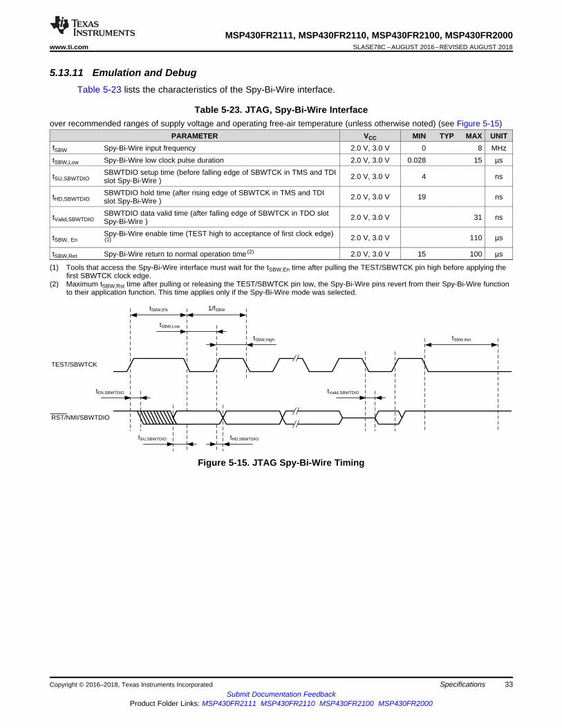
5.13.11 Emulation and DebugTable 5-23 lists the characteristics of the Spy-Bi-Wire interface.
(1) Tools that access the Spy-Bi-Wire interface must wait for the tSBW,En time after pulling the TEST/SBWTCK pin high before applying thefirst SBWTCK clock edge.
(2) Maximum tSBW,Rst time after pulling or releasing the TEST/SBWTCK pin low, the Spy-Bi-Wire pins revert from their Spy-Bi-Wire functionto their application function. This time applies only if the Spy-Bi-Wire mode was selected.
Table 5-23. JTAG, Spy-Bi-Wire Interfaceover recommended ranges of supply voltage and operating free-air temperature (unless otherwise noted) (see Figure 5-15)
PARAMETER VCC MIN TYP MAX UNITfSBW Spy-Bi-Wire input frequency 2.0 V, 3.0 V 0 8 MHztSBW,Low Spy-Bi-Wire low clock pulse duration 2.0 V, 3.0 V 0.028 15 µs
tSU,SBWTDIOSBWTDIO setup time (before falling edge of SBWTCK in TMS and TDIslot Spy-Bi-Wire ) 2.0 V, 3.0 V 4 ns
tHD,SBWTDIOSBWTDIO hold time (after rising edge of SBWTCK in TMS and TDIslot Spy-Bi-Wire ) 2.0 V, 3.0 V 19 ns
tValid,SBWTDIOSBWTDIO data valid time (after falling edge of SBWTCK in TDO slotSpy-Bi-Wire ) 2.0 V, 3.0 V 31 ns
tSBW, EnSpy-Bi-Wire enable time (TEST high to acceptance of first clock edge)(1) 2.0 V, 3.0 V 110 µs
tSBW,Ret Spy-Bi-Wire return to normal operation time (2) 2.0 V, 3.0 V 15 100 µs
Figure 5-15. JTAG Spy-Bi-Wire Timing
TCK
1/fTCK
tSU,TMStHD,TMS
tTCK,HightTCK,Low
TEST
tJTAG,Ret
TMS
TDO
tZ-Valid,TDO tValid,TDO tValid-Z,TDO
tSU,TDItHD,TDI
TDI(or TDO as TDI)
34
MSP430FR2111, MSP430FR2110, MSP430FR2100, MSP430FR2000SLASE78C –AUGUST 2016–REVISED AUGUST 2018 www.ti.com
Submit Documentation FeedbackProduct Folder Links: MSP430FR2111 MSP430FR2110 MSP430FR2100 MSP430FR2000
Specifications Copyright © 2016–2018, Texas Instruments Incorporated
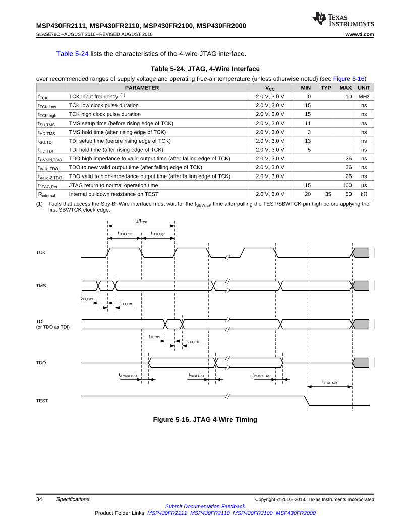
Table 5-24 lists the characteristics of the 4-wire JTAG interface.
(1) Tools that access the Spy-Bi-Wire interface must wait for the tSBW,En time after pulling the TEST/SBWTCK pin high before applying thefirst SBWTCK clock edge.
Table 5-24. JTAG, 4-Wire Interfaceover recommended ranges of supply voltage and operating free-air temperature (unless otherwise noted) (see Figure 5-16)
PARAMETER VCC MIN TYP MAX UNITfTCK TCK input frequency (1) 2.0 V, 3.0 V 0 10 MHztTCK,Low TCK low clock pulse duration 2.0 V, 3.0 V 15 nstTCK,high TCK high clock pulse duration 2.0 V, 3.0 V 15 nstSU,TMS TMS setup time (before rising edge of TCK) 2.0 V, 3.0 V 11 nstHD,TMS TMS hold time (after rising edge of TCK) 2.0 V, 3.0 V 3 nstSU,TDI TDI setup time (before rising edge of TCK) 2.0 V, 3.0 V 13 nstHD,TDI TDI hold time (after rising edge of TCK) 2.0 V, 3.0 V 5 nstz-Valid,TDO TDO high impedance to valid output time (after falling edge of TCK) 2.0 V, 3.0 V 26 nstValid,TDO TDO to new valid output time (after falling edge of TCK) 2.0 V, 3.0 V 26 nstValid-Z,TDO TDO valid to high-impedance output time (after falling edge of TCK) 2.0 V, 3.0 V 26 nstJTAG,Ret JTAG return to normal operation time 15 100 µsRinternal Internal pulldown resistance on TEST 2.0 V, 3.0 V 20 35 50 kΩ
Figure 5-16. JTAG 4-Wire Timing
35
MSP430FR2111, MSP430FR2110, MSP430FR2100, MSP430FR2000www.ti.com SLASE78C –AUGUST 2016–REVISED AUGUST 2018
Submit Documentation FeedbackProduct Folder Links: MSP430FR2111 MSP430FR2110 MSP430FR2100 MSP430FR2000
Detailed DescriptionCopyright © 2016–2018, Texas Instruments Incorporated
6 Detailed Description
6.1 OverviewThe Texas Instruments MSP430FR211x family of ultra-low-power microcontrollers consists of severaldevices featuring different sets of peripherals. The architecture, combined with five low-power modes, isoptimized to achieve extended battery life (for example, in portable measurement applications). Thedevices feature a powerful 16-bit RISC CPU, 16-bit register, and constant generators that contribute tomaximum code efficiency.
The MSP430FR211x devices are microcontroller configurations with one Timer_B, eCOMP with built-in 6-bit DAC as an internal reference voltage, a high-performance 10-bit ADC, an eUSCI that supports UARTand SPI, an RTC module with alarm capabilities, and up to 12 I/O pins.
6.2 CPUThe MSP430 CPU has a 16-bit RISC architecture that is highly transparent to the application. Alloperations, other than program-flow instructions, are performed as register operations in conjunction withseven addressing modes for source operand and four addressing modes for destination operand.
The CPU is integrated with 16 registers that provide reduced instruction execution time. The register-to-register operation execution time is one cycle of the CPU clock.
Four of the registers, R0 to R3, are dedicated as program counter (PC), stack pointer (SP), status register(SR), and constant generator (CG), respectively. The remaining registers are general-purpose registers.
Peripherals are connected to the CPU using data, address, and control buses. Peripherals can bemanaged with all instructions.
6.3 Operating ModesThe MSP430 has one active mode and several software selectable low-power modes of operation (seeTable 6-1). An interrupt event can wake up the device from low-power mode LPM0, LPM3 or LPM4,service the request, and restore back to the low-power mode on return from the interrupt program. Low-power modes LPM3.5 and LPM4.5 disable the core supply to minimize power consumption.
NOTEXT1CLK and VLOCLK can be active during LPM4 if requested by low-frequency peripherals.
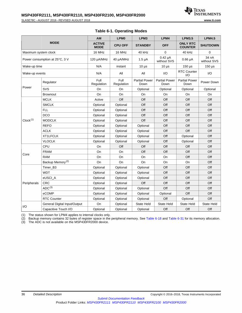
36
MSP430FR2111, MSP430FR2110, MSP430FR2100, MSP430FR2000SLASE78C –AUGUST 2016–REVISED AUGUST 2018 www.ti.com
Submit Documentation FeedbackProduct Folder Links: MSP430FR2111 MSP430FR2110 MSP430FR2100 MSP430FR2000
Detailed Description Copyright © 2016–2018, Texas Instruments Incorporated
(1) The status shown for LPM4 applies to internal clocks only.(2) Backup memory contains 32 bytes of register space in the peripheral memory. See Table 6-18 and Table 6-31 for its memory allocation.(3) The ADC is not available on the MSP430FR2000 device.
Table 6-1. Operating Modes
MODEAM LPM0 LPM3 LPM4 LPM3.5 LPM4.5
ACTIVEMODE CPU OFF STANDBY OFF ONLY RTC
COUNTER SHUTDOWN
Maximum system clock 16 MHz 16 MHz 40 kHz 0 40 kHz 0
Power consumption at 25°C, 3 V 120 µA/MHz 40 µA/MHz 1.5 µA 0.42 µAwithout SVS 0.66 µA 34 nA
without SVSWake-up time N/A instant 10 µs 10 µs 150 µs 150 µs
Wake-up events N/A All All I/O RTC CounterI/O I/O
PowerRegulator Full
RegulationFull
RegulationPartial Power
DownPartial Power
DownPartial Power
Down Power Down
SVS On On Optional Optional Optional OptionalBrownout On On On On On On
Clock (1)
MCLK Active Off Off Off Off OffSMCLK Optional Optional Off Off Off OffFLL Optional Optional Off Off Off OffDCO Optional Optional Off Off Off OffMODCLK Optional Optional Off Off Off OffREFO Optional Optional Optional Off Off OffACLK Optional Optional Optional Off Off OffXT1LFCLK Optional Optional Optional Off Optional OffVLOCLK Optional Optional Optional Off Optional Off
Core
CPU On Off Off Off Off OffFRAM On On Off Off Off OffRAM On On On On Off OffBackup Memory (2) On On On On On Off
Peripherals
Timer_B3 Optional Optional Optional Off Off OffWDT Optional Optional Optional Off Off OffeUSCI_A Optional Optional Optional Off Off OffCRC Optional Optional Off Off Off OffADC (3) Optional Optional Optional Off Off OffeCOMP Optional Optional Optional Optional Off OffRTC Counter Optional Optional Optional Off Optional Off
I/OGeneral Digital Input/Output On Optional State Held State Held State Held State HeldCapacitive Touch I/O Optional Optional Optional Off Off Off
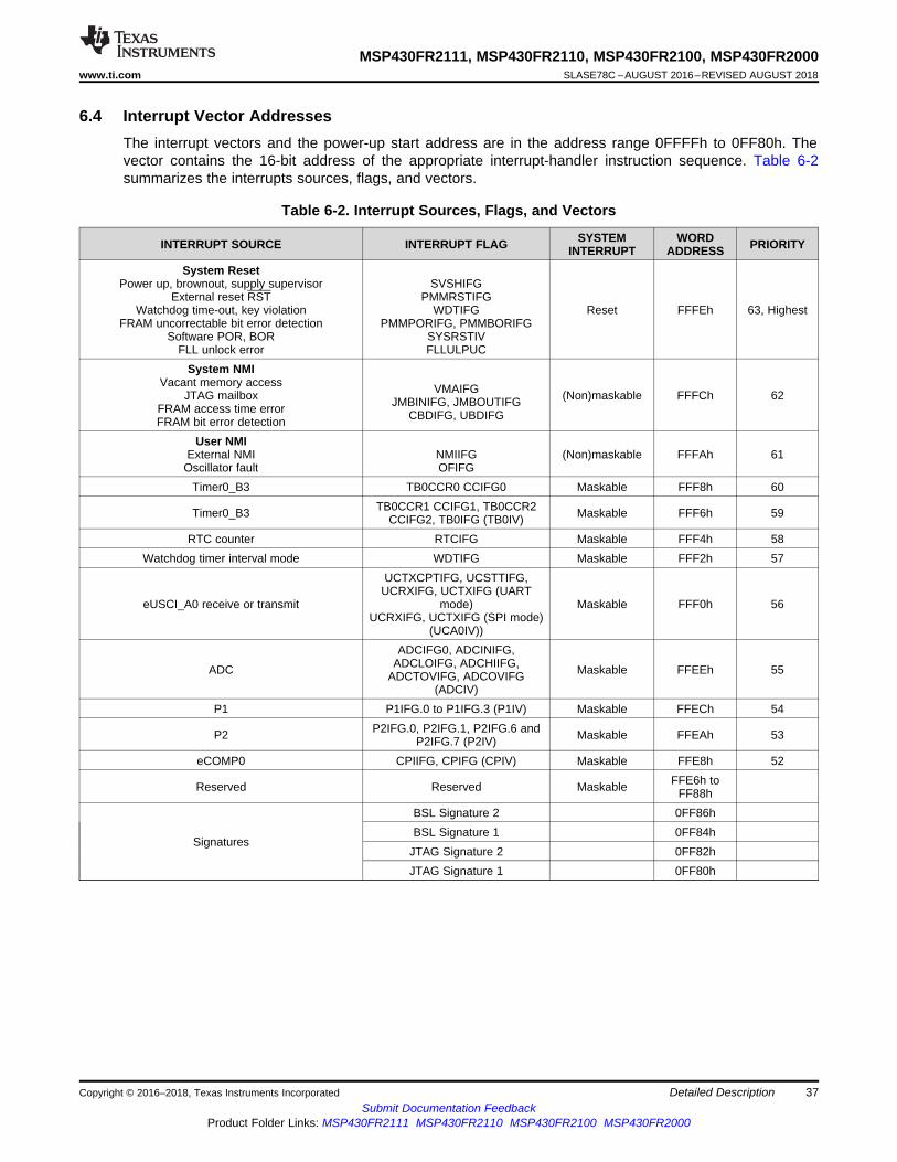
37
MSP430FR2111, MSP430FR2110, MSP430FR2100, MSP430FR2000www.ti.com SLASE78C –AUGUST 2016–REVISED AUGUST 2018
Submit Documentation FeedbackProduct Folder Links: MSP430FR2111 MSP430FR2110 MSP430FR2100 MSP430FR2000
Detailed DescriptionCopyright © 2016–2018, Texas Instruments Incorporated
6.4 Interrupt Vector AddressesThe interrupt vectors and the power-up start address are in the address range 0FFFFh to 0FF80h. Thevector contains the 16-bit address of the appropriate interrupt-handler instruction sequence. Table 6-2summarizes the interrupts sources, flags, and vectors.
Table 6-2. Interrupt Sources, Flags, and Vectors
INTERRUPT SOURCE INTERRUPT FLAG SYSTEMINTERRUPT
WORDADDRESS PRIORITY
System ResetPower up, brownout, supply supervisor
External reset RSTWatchdog time-out, key violation
FRAM uncorrectable bit error detectionSoftware POR, BOR
FLL unlock error
SVSHIFGPMMRSTIFG
WDTIFGPMMPORIFG, PMMBORIFG
SYSRSTIVFLLULPUC
Reset FFFEh 63, Highest
System NMIVacant memory access
JTAG mailboxFRAM access time errorFRAM bit error detection
VMAIFGJMBINIFG, JMBOUTIFG
CBDIFG, UBDIFG
(Non)maskable FFFCh 62
User NMIExternal NMI
Oscillator faultNMIIFGOFIFG
(Non)maskable FFFAh 61
Timer0_B3 TB0CCR0 CCIFG0 Maskable FFF8h 60
Timer0_B3 TB0CCR1 CCIFG1, TB0CCR2CCIFG2, TB0IFG (TB0IV) Maskable FFF6h 59
RTC counter RTCIFG Maskable FFF4h 58Watchdog timer interval mode WDTIFG Maskable FFF2h 57
eUSCI_A0 receive or transmit
UCTXCPTIFG, UCSTTIFG,UCRXIFG, UCTXIFG (UART
mode)UCRXIFG, UCTXIFG (SPI mode)
(UCA0IV))
Maskable FFF0h 56
ADC
ADCIFG0, ADCINIFG,ADCLOIFG, ADCHIIFG,
ADCTOVIFG, ADCOVIFG(ADCIV)
Maskable FFEEh 55
P1 P1IFG.0 to P1IFG.3 (P1IV) Maskable FFECh 54
P2 P2IFG.0, P2IFG.1, P2IFG.6 andP2IFG.7 (P2IV) Maskable FFEAh 53
eCOMP0 CPIIFG, CPIFG (CPIV) Maskable FFE8h 52
Reserved Reserved Maskable FFE6h toFF88h
Signatures
BSL Signature 2 0FF86hBSL Signature 1 0FF84h
JTAG Signature 2 0FF82hJTAG Signature 1 0FF80h
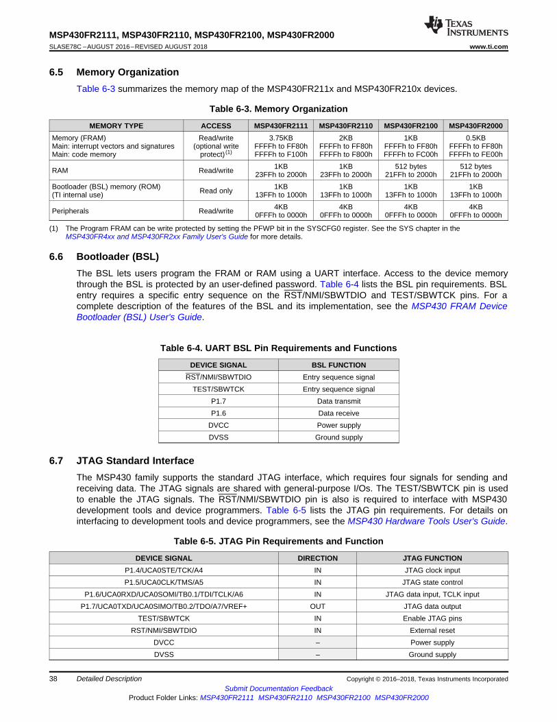
38
MSP430FR2111, MSP430FR2110, MSP430FR2100, MSP430FR2000SLASE78C –AUGUST 2016–REVISED AUGUST 2018 www.ti.com
Submit Documentation FeedbackProduct Folder Links: MSP430FR2111 MSP430FR2110 MSP430FR2100 MSP430FR2000
Detailed Description Copyright © 2016–2018, Texas Instruments Incorporated
(1) The Program FRAM can be write protected by setting the PFWP bit in the SYSCFG0 register. See the SYS chapter in theMSP430FR4xx and MSP430FR2xx Family User's Guide for more details.
6.5 Memory OrganizationTable 6-3 summarizes the memory map of the MSP430FR211x and MSP430FR210x devices.
Table 6-3. Memory Organization
MEMORY TYPE ACCESS MSP430FR2111 MSP430FR2110 MSP430FR2100 MSP430FR2000Memory (FRAM)Main: interrupt vectors and signaturesMain: code memory
Read/write(optional write
protect) (1)
3.75KBFFFFh to FF80hFFFFh to F100h
2KBFFFFh to FF80hFFFFh to F800h
1KBFFFFh to FF80hFFFFh to FC00h
0.5KBFFFFh to FF80hFFFFh to FE00h
RAM Read/write 1KB23FFh to 2000h
1KB23FFh to 2000h
512 bytes21FFh to 2000h
512 bytes21FFh to 2000h
Bootloader (BSL) memory (ROM)(TI internal use) Read only 1KB
13FFh to 1000h1KB
13FFh to 1000h1KB
13FFh to 1000h1KB
13FFh to 1000h
Peripherals Read/write 4KB0FFFh to 0000h
4KB0FFFh to 0000h
4KB0FFFh to 0000h
4KB0FFFh to 0000h
6.6 Bootloader (BSL)The BSL lets users program the FRAM or RAM using a UART interface. Access to the device memorythrough the BSL is protected by an user-defined password. Table 6-4 lists the BSL pin requirements. BSLentry requires a specific entry sequence on the RST/NMI/SBWTDIO and TEST/SBWTCK pins. For acomplete description of the features of the BSL and its implementation, see the MSP430 FRAM DeviceBootloader (BSL) User's Guide.
Table 6-4. UART BSL Pin Requirements and Functions
DEVICE SIGNAL BSL FUNCTIONRST/NMI/SBWTDIO Entry sequence signal
TEST/SBWTCK Entry sequence signalP1.7 Data transmitP1.6 Data receive
DVCC Power supplyDVSS Ground supply
6.7 JTAG Standard InterfaceThe MSP430 family supports the standard JTAG interface, which requires four signals for sending andreceiving data. The JTAG signals are shared with general-purpose I/Os. The TEST/SBWTCK pin is usedto enable the JTAG signals. The RST/NMI/SBWTDIO pin is also is required to interface with MSP430development tools and device programmers. Table 6-5 lists the JTAG pin requirements. For details oninterfacing to development tools and device programmers, see the MSP430 Hardware Tools User's Guide.
Table 6-5. JTAG Pin Requirements and Function
DEVICE SIGNAL DIRECTION JTAG FUNCTIONP1.4/UCA0STE/TCK/A4 IN JTAG clock inputP1.5/UCA0CLK/TMS/A5 IN JTAG state control
P1.6/UCA0RXD/UCA0SOMI/TB0.1/TDI/TCLK/A6 IN JTAG data input, TCLK inputP1.7/UCA0TXD/UCA0SIMO/TB0.2/TDO/A7/VREF+ OUT JTAG data output
TEST/SBWTCK IN Enable JTAG pinsRST/NMI/SBWTDIO IN External reset
DVCC – Power supplyDVSS – Ground supply
39
MSP430FR2111, MSP430FR2110, MSP430FR2100, MSP430FR2000www.ti.com SLASE78C –AUGUST 2016–REVISED AUGUST 2018
Submit Documentation FeedbackProduct Folder Links: MSP430FR2111 MSP430FR2110 MSP430FR2100 MSP430FR2000
Detailed DescriptionCopyright © 2016–2018, Texas Instruments Incorporated
6.8 Spy-Bi-Wire Interface (SBW)The MSP430 family supports the 2-wire Spy-Bi-Wire interface. Spy-Bi-Wire can be used to interface withMSP430 development tools and device programmers. Table 6-6 lists the Spy-Bi-Wire interface pinrequirements. For further details on interfacing to development tools and device programmers, see theMSP430 Hardware Tools User's Guide.
Table 6-6. Spy-Bi-Wire Pin Requirements and Functions
DEVICE SIGNAL DIRECTION SBW FUNCTIONTEST/SBWTCK IN Spy-Bi-Wire clock input
RST/NMI/SBWTDIO IN, OUT Spy-Bi-Wire data input and outputVCC Power supplyVSS Ground supply
6.9 FRAMThe FRAM can be programmed using the JTAG port, Spy-Bi-Wire (SBW), the BSL, or in-system by theCPU. Features of the FRAM include:• Byte and word access capability• Programmable wait state generation• Error correction coding (ECC)
6.10 Memory ProtectionThe device features memory protection of user access authority and write protection include:• Securing the whole memory map to prevent unauthorized access from JTAG port or BSL, by writing
JTAG and BSL signatures using the JTAG port, SBW, the BSL, or in-system by the CPU.• Write protection enabled to prevent unwanted write operation to FRAM contents by setting the control
bits with accordingly password in System Configuration register 0. For more detailed information, seethe SYS chapter in the MSP430FR4xx and MSP430FR2xx Family User's Guide.
6.11 PeripheralsPeripherals are connected to the CPU through data, address, and control buses. All peripherals can behandled by using all instructions in the memory map. For complete module description, see theMSP430FR4xx and MSP430FR2xx Family User's Guide.
6.11.1 Power-Management Module (PMM) and On-Chip Reference VoltagesThe PMM includes an integrated voltage regulator that supplies the core voltage to the device. The PMMalso includes supply voltage supervisor (SVS) and brownout protection. The brownout reset circuit (BOR)is implemented to provide the proper internal reset signal to the device during power on and power off.The SVS circuitry detects if the supply voltage drops below a user-selectable safe level. SVS circuitry isavailable on the primary supply.
The device contains two on-chip references: 1.5 V for internal reference and 1.2 V for external reference.
The 1.5-V reference is internally connected to ADC channel 13. DVCC is internally connected to ADCchannel 15. When DVCC is set as the reference voltage for ADC conversion, the DVCC can be easilyrepresent as Equation 1 by using the ADC sampling the 1.5-V reference without any external componentssupport.DVCC = (1023 × 1.5 V) / 1.5-V Reference ADC result (1)
40
MSP430FR2111, MSP430FR2110, MSP430FR2100, MSP430FR2000SLASE78C –AUGUST 2016–REVISED AUGUST 2018 www.ti.com
Submit Documentation FeedbackProduct Folder Links: MSP430FR2111 MSP430FR2110 MSP430FR2100 MSP430FR2000
Detailed Description Copyright © 2016–2018, Texas Instruments Incorporated
(1) The ADC is not available on the MSP430FR2000 device.(2) Controlled by the RTCCKSEL bit in the SYSCFG2 register.
The 1.5-V reference is also internally connected to the comparator built-in DAC as reference voltage.DVCC is internally connected to another source of the DAC reference, and both are controlled by theCPDACREFS bit. For more detailed information, see the Comparator chapter of the MSP430FR4xx andMSP430FR2xx Family User's Guide.
A 1.2-V reference voltage can be buffered and output to P1.7/TDO/A7/VREF+, when EXTREFEN = 1 inthe PMMCTL2 register. ADC channel 7 can also be selected to monitor this voltage. For more detailedinformation, see the MSP430FR4xx and MSP430FR2xx Family User's Guide.
NOTEThe ADC is not available on the MSP430FR2000 device.
6.11.2 Clock System (CS) and Clock DistributionThe clock system includes a 32-kHz low-frequency oscillator (XT1), an internal very-low-power low-frequency oscillator (VLO), an integrated 32-kHz RC oscillator (REFO), an integrated internal digitallycontrolled oscillator (DCO) that may use frequency-locked loop (FLL) locking with an internal or external32-kHz reference clock, and on-chip asynchronous high-speed clock (MODOSC). The clock system isdesigned to target cost-effective designs with minimal external components. A fail-safe mechanism isdesigned for XT1. The clock system module offers the following clock signals.• Main Clock (MCLK): the system clock used by the CPU and all relevant peripherals accessed by the
bus. All clock sources except MODOSC can be selected as the source with a predivider of 1, 2, 4, 8,16, 32, 64, or 128.
• Sub-Main Clock (SMCLK): the subsystem clock used by the peripheral modules. SMCLK derives fromthe MCLK with a predivider of 1, 2, 4, or 8. This means SMCLK is always equal to or less than MCLK.
• Auxiliary Clock (ACLK): this clock is derived from the external XT1 clock or internal REFO clock up to40 kHz.
All peripherals may have one or several clock sources depending on specific functionality. Table 6-7 andTable 6-8 summarize the clock distribution used in this device.
Table 6-7. Clock Distribution
CLOCKSOURCE
SELECT BITSMCLK SMCLK ACLK MODCLK VLOCLK EXTERNAL PIN
FrequencyRange DC to 16 MHz DC to 16 MHz DC to 40 kHz 4 MHz 10 kHz
CPU N/A DefaultFRAM N/A DefaultRAM N/A DefaultCRC N/A DefaultI/O N/A DefaultTB0 TBSSEL 10b 01b 00b (TB0CLK pin)eUSCI_A0 UCSSEL 10b or 11b 01b 00b (UCA0CLK pin)WDT WDTSSEL 00b 01b 10bADC (1) ADCSSEL 10b or 11b 01b 00bRTC RTCSS 01b (2) 01b (2) 11b
41
MSP430FR2111, MSP430FR2110, MSP430FR2100, MSP430FR2000www.ti.com SLASE78C –AUGUST 2016–REVISED AUGUST 2018
Submit Documentation FeedbackProduct Folder Links: MSP430FR2111 MSP430FR2110 MSP430FR2100 MSP430FR2000
Detailed DescriptionCopyright © 2016–2018, Texas Instruments Incorporated
Table 6-8. XTCLK Distribution
OPERATION MODE CLOCK SOURCESELECT BITS
XTLFCLKAM TO LPM3.5 (DC to 40 kHz)
MCLK SELMS 10bSMCLK SELMS 10bREFO SELREF 0bACLK SELA 0bRTC RTCSS 10b
6.11.3 General-Purpose Input/Output Port (I/O)Up to 12 I/O ports are implemented.• P1 has 8 bits implemented, and P2 has 4 bits implemented.• All individual I/O bits are independently programmable.• Any combination of input, output, and interrupt conditions is possible to P1 and P2.• Programmable pullup or pulldown on all ports.• Edge-selectable interrupt, LPM4, LPM3.5 and LPM4.5 wake-up input capability is available for P1.0 to
P1.3, P2.0, P2.1, P2.6, and P2.7.• Read and write access to port-control registers is supported by all instructions.• Ports can be accessed byte-wise or word-wise in pairs.• Capacitive Touch I/O functionality is supported on all pins.
NOTEConfiguration of digital I/Os after BOR reset
To prevent any cross currents during start-up of the device, all port pins are high-impedancewith Schmitt triggers and module functions disabled. To enable the I/O functions after a BORreset, the ports must be configured first and then the LOCKLPM5 bit must be cleared. Fordetails, see the Configuration After Reset section in the Digital I/O chapter of theMSP430FR4xx and MSP430FR2xx Family User's Guide.
6.11.4 Watchdog Timer (WDT)The primary function of the WDT module is to perform a controlled system restart after a software problemoccurs. If the selected time interval expires, a system reset is generated. If the watchdog function is notneeded in an application, the module can be configured as interval timer and can generate interrupts atselected time intervals.
Table 6-9. WDT Clocks
WDTSSEL NORMAL OPERATION(WATCHDOG AND INTERVAL TIMER MODE)
00 SMCLK01 ACLK10 VLOCLK11 Reserved
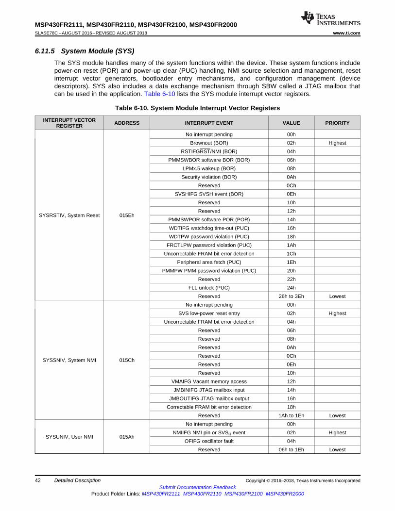
42
MSP430FR2111, MSP430FR2110, MSP430FR2100, MSP430FR2000SLASE78C –AUGUST 2016–REVISED AUGUST 2018 www.ti.com
Submit Documentation FeedbackProduct Folder Links: MSP430FR2111 MSP430FR2110 MSP430FR2100 MSP430FR2000
Detailed Description Copyright © 2016–2018, Texas Instruments Incorporated
6.11.5 System Module (SYS)The SYS module handles many of the system functions within the device. These system functions includepower-on reset (POR) and power-up clear (PUC) handling, NMI source selection and management, resetinterrupt vector generators, bootloader entry mechanisms, and configuration management (devicedescriptors). SYS also includes a data exchange mechanism through SBW called a JTAG mailbox thatcan be used in the application. Table 6-10 lists the SYS module interrupt vector registers.
Table 6-10. System Module Interrupt Vector Registers
INTERRUPT VECTORREGISTER ADDRESS INTERRUPT EVENT VALUE PRIORITY
SYSRSTIV, System Reset 015Eh
No interrupt pending 00hBrownout (BOR) 02h Highest
RSTIFGRST/NMI (BOR) 04hPMMSWBOR software BOR (BOR) 06h
LPMx.5 wakeup (BOR) 08hSecurity violation (BOR) 0Ah
Reserved 0ChSVSHIFG SVSH event (BOR) 0Eh
Reserved 10hReserved 12h
PMMSWPOR software POR (POR) 14hWDTIFG watchdog time-out (PUC) 16hWDTPW password violation (PUC) 18h
FRCTLPW password violation (PUC) 1AhUncorrectable FRAM bit error detection 1Ch
Peripheral area fetch (PUC) 1EhPMMPW PMM password violation (PUC) 20h
Reserved 22hFLL unlock (PUC) 24h
Reserved 26h to 3Eh Lowest
SYSSNIV, System NMI 015Ch
No interrupt pending 00hSVS low-power reset entry 02h Highest
Uncorrectable FRAM bit error detection 04hReserved 06hReserved 08hReserved 0AhReserved 0ChReserved 0EhReserved 10h
VMAIFG Vacant memory access 12hJMBINIFG JTAG mailbox input 14h
JMBOUTIFG JTAG mailbox output 16hCorrectable FRAM bit error detection 18h
Reserved 1Ah to 1Eh Lowest
SYSUNIV, User NMI 015Ah
No interrupt pending 00hNMIIFG NMI pin or SVSH event 02h Highest
OFIFG oscillator fault 04hReserved 06h to 1Eh Lowest
43
MSP430FR2111, MSP430FR2110, MSP430FR2100, MSP430FR2000www.ti.com SLASE78C –AUGUST 2016–REVISED AUGUST 2018
Submit Documentation FeedbackProduct Folder Links: MSP430FR2111 MSP430FR2110 MSP430FR2100 MSP430FR2000
Detailed DescriptionCopyright © 2016–2018, Texas Instruments Incorporated
(1) This is the remapped functionality controlled by the USCIARMP bit in the SYSCFG3 register. Only one selected port is valid at the sametime.
6.11.6 Cyclic Redundancy Check (CRC)The 16-bit CRC module produces a signature based on a sequence of data values and can be used fordata checking purposes. The CRC generation polynomial is compliant with CRC-16-CCITT standard ofx16 + x12 + x5 + 1.
6.11.7 Enhanced Universal Serial Communication Interface (eUSCI_A0)The eUSCI modules are used for serial data communications. The eUSCI_A module supports eitherUART or SPI communications. Additionally, eUSCI_A supports automatic baud-rate detection and IrDA.
Table 6-11. eUSCI Pin Configurations
eUSCI_A0
PIN (USCIARMP = 0) UART SPIP1.7 TXD SIMOP1.6 RXD SOMIP1.5 SCLKP1.4 STE
PIN (USCIARMP = 1) UART SPIP1.3 (1) TXD SIMOP1.2 (1) RXD SOMIP1.1 (1) SCLKP1.0 (1) STE
44
MSP430FR2111, MSP430FR2110, MSP430FR2100, MSP430FR2000SLASE78C –AUGUST 2016–REVISED AUGUST 2018 www.ti.com
Submit Documentation FeedbackProduct Folder Links: MSP430FR2111 MSP430FR2110 MSP430FR2100 MSP430FR2000
Detailed Description Copyright © 2016–2018, Texas Instruments Incorporated
(1) This is the remapped functionality controlled by the TBRMP bit in the SYSCFG3 register. Only one selected port is valid at the sametime when TB0 acts as capture input functionality. TB0 PWM outputs regardless of the setting on this remap bit.
(2) The ADC is not available on the MSP430FR2000 device.
6.11.8 Timers (Timer0_B3)The Timer0_B3 module is 16-bit timer and counter with three capture/compare registers. The timer cansupport multiple captures or compares, PWM outputs, and interval timing (see Table 6-12). Timer0_B3has extensive interrupt capabilities. Interrupts may be generated from the counter on overflow conditionsand from each of the capture/compare registers. The CCR0 register on Timer0_B3 is not externallyconnected and can be used only for hardware period timing and interrupt generation. In Up Mode, it canbe used to set the overflow value of the counter.
Table 6-12. Timer0_B3 Signal Connections
PORT PIN DEVICE INPUTSIGNAL
MODULE INPUTNAME MODULE BLOCK MODULE OUTPUT
SIGNALDEVICE OUTPUT
SIGNALP2.7 TB0CLK TBCLK
Timer N/AACLK (internal) ACLK
SMCLK (internal) SMCLKFrom Capacitive
Touch I/O (internal) INCLK
From RTC (internal) CCI0A
CCR0 TB0ACLK (internal) CCI0B
DVSS GNDDVCC VCC
P1.6 (TBRMP = 0)TB0.1 CCI1A
CCR1 TB1
TB0.1P2.0 (TBRMP = 1) (1)
From eCOMP(internal) CCI1B To ADC trigger (2)
DVSS GNDDVCC VCC
P1.7 (TBRMP = 0)TB0.2 CCI2A
CCR2 TB2
TB0.2P2.1 (TBRMP = 1) (1)
From CapacitiveTouch I/O (internal) CCI2B
DVSS GNDDVCC VCC
The interconnection of Timer0_B3 can be used to modulate the eUSCI_A pin of UCA0TXD/UCA0SIMO ineither ASK or part of FSK mode, with which a user can easily acquire a modulated infrared command fordirectly driving an external IR diode. The IR functions are fully controlled by SYSCFG1 including IREN(enable), IRPSEL (polarity select), IRMSEL (mode select), IRDSEL (data select), and IRDATA (data) bits.For more information, see the SYS chapter in the MSP430FR4xx and MSP430FR2xx Family User'sGuide.
The Timer_B module can put all Timer_B outputs into a high-impedance state when the selected source istriggered. The source can be selected from external pin or internal of the device, which is controlled byTB0TRG in SYS. For more information, see the SYS chapter in the MSP430FR4xx and MSP430FR2xxFamily User's Guide.
45
MSP430FR2111, MSP430FR2110, MSP430FR2100, MSP430FR2000www.ti.com SLASE78C –AUGUST 2016–REVISED AUGUST 2018
Submit Documentation FeedbackProduct Folder Links: MSP430FR2111 MSP430FR2110 MSP430FR2100 MSP430FR2000
Detailed DescriptionCopyright © 2016–2018, Texas Instruments Incorporated
Table 6-13 summarizes the selection of the Timer_B high-impedance trigger.
(1) When TB0 is set to PWM output function, both port groups can receive the output, and the output iscontrolled by only the PxSEL.y bits.
Table 6-13. TBxOUTH
TB0TRGSEL TB0OUTH TRIGGER SOURCESELECTION Timer_B PAD OUTPUT HIGH IMPEDANCE
TB0TRGSEL = 0 eCOMP0 output (internal)P1.6, P1.7, P2.0, P2.1 (1)
TB0TRGSEL= 1 P1.2
6.11.9 Backup Memory (BAKMEM)The BAKMEM supports data retention functionality during LPM3.5 mode. This device provides up to 32bytes that are retained during LPM3.5.
6.11.10 Real-Time Clock (RTC) CounterThe RTC counter is a 16-bit modulo counter that is functional in AM, LPM0, LPM3, LPM4, and LPM3.5.This module may periodically wake up the CPU from LPM0, LPM3, LPM4, or LPM3.5 based on timingfrom a low-power clock source such as XT1, ACLK, or VLO. In AM, RTC can be driven by SMCLK togenerate high-frequency timing events and interrupts. ACLK and SMCLK both can source to the RTC;however, only one of them can be selected at any given time. The RTC overflow events trigger:• Timer0_B3 CCR0A• ADC conversion trigger when ADCSHSx bits are set as 01b
6.11.11 10-Bit Analog-to-Digital Converter (ADC)The 10-bit ADC module supports fast 10-bit analog-to-digital conversions with single-ended input. Themodule implements a 10-bit SAR core, sample select control, reference generator, and a conversion resultbuffer. A window comparator with lower and upper limits allows CPU-independent result monitoring withthree window comparator interrupt flags.
NOTEThe ADC is not available on the MSP430FR2000 device.
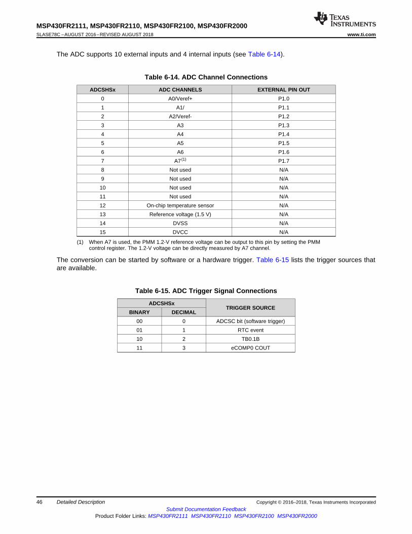
46
MSP430FR2111, MSP430FR2110, MSP430FR2100, MSP430FR2000SLASE78C –AUGUST 2016–REVISED AUGUST 2018 www.ti.com
Submit Documentation FeedbackProduct Folder Links: MSP430FR2111 MSP430FR2110 MSP430FR2100 MSP430FR2000
Detailed Description Copyright © 2016–2018, Texas Instruments Incorporated
The ADC supports 10 external inputs and 4 internal inputs (see Table 6-14).
(1) When A7 is used, the PMM 1.2-V reference voltage can be output to this pin by setting the PMMcontrol register. The 1.2-V voltage can be directly measured by A7 channel.
Table 6-14. ADC Channel Connections
ADCSHSx ADC CHANNELS EXTERNAL PIN OUT0 A0/Veref+ P1.01 A1/ P1.12 A2/Veref- P1.23 A3 P1.34 A4 P1.45 A5 P1.56 A6 P1.67 A7 (1) P1.78 Not used N/A9 Not used N/A10 Not used N/A11 Not used N/A12 On-chip temperature sensor N/A13 Reference voltage (1.5 V) N/A14 DVSS N/A15 DVCC N/A
The conversion can be started by software or a hardware trigger. Table 6-15 lists the trigger sources thatare available.
Table 6-15. ADC Trigger Signal Connections
ADCSHSxTRIGGER SOURCE
BINARY DECIMAL00 0 ADCSC bit (software trigger)01 1 RTC event10 2 TB0.1B11 3 eCOMP0 COUT
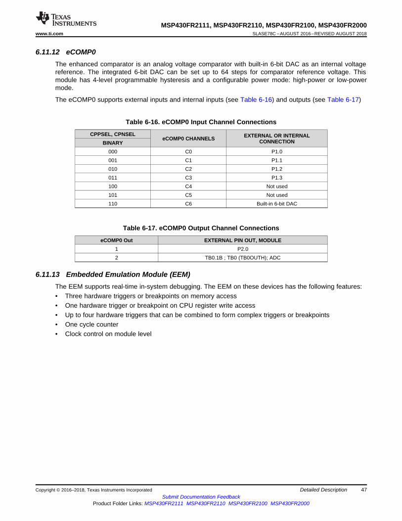
47
MSP430FR2111, MSP430FR2110, MSP430FR2100, MSP430FR2000www.ti.com SLASE78C –AUGUST 2016–REVISED AUGUST 2018
Submit Documentation FeedbackProduct Folder Links: MSP430FR2111 MSP430FR2110 MSP430FR2100 MSP430FR2000
Detailed DescriptionCopyright © 2016–2018, Texas Instruments Incorporated
6.11.12 eCOMP0The enhanced comparator is an analog voltage comparator with built-in 6-bit DAC as an internal voltagereference. The integrated 6-bit DAC can be set up to 64 steps for comparator reference voltage. Thismodule has 4-level programmable hysteresis and a configurable power mode: high-power or low-powermode.
The eCOMP0 supports external inputs and internal inputs (see Table 6-16) and outputs (see Table 6-17)
Table 6-16. eCOMP0 Input Channel Connections
CPPSEL, CPNSELeCOMP0 CHANNELS EXTERNAL OR INTERNAL
CONNECTIONBINARY000 C0 P1.0001 C1 P1.1010 C2 P1.2011 C3 P1.3100 C4 Not used101 C5 Not used110 C6 Built-in 6-bit DAC
Table 6-17. eCOMP0 Output Channel Connections
eCOMP0 Out EXTERNAL PIN OUT, MODULE1 P2.02 TB0.1B ; TB0 (TB0OUTH); ADC
6.11.13 Embedded Emulation Module (EEM)The EEM supports real-time in-system debugging. The EEM on these devices has the following features:• Three hardware triggers or breakpoints on memory access• One hardware trigger or breakpoint on CPU register write access• Up to four hardware triggers that can be combined to form complex triggers or breakpoints• One cycle counter• Clock control on module level
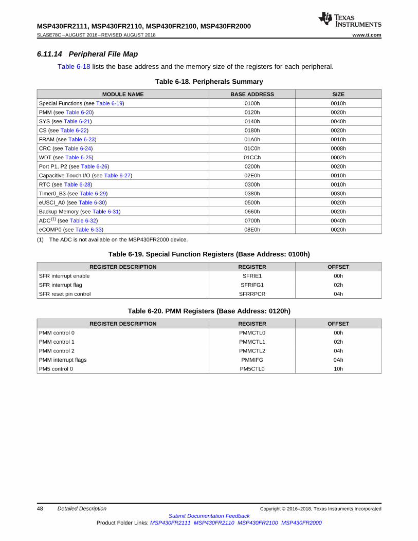
48
MSP430FR2111, MSP430FR2110, MSP430FR2100, MSP430FR2000SLASE78C –AUGUST 2016–REVISED AUGUST 2018 www.ti.com
Submit Documentation FeedbackProduct Folder Links: MSP430FR2111 MSP430FR2110 MSP430FR2100 MSP430FR2000
Detailed Description Copyright © 2016–2018, Texas Instruments Incorporated
(1) The ADC is not available on the MSP430FR2000 device.
6.11.14 Peripheral File MapTable 6-18 lists the base address and the memory size of the registers for each peripheral.
Table 6-18. Peripherals Summary
MODULE NAME BASE ADDRESS SIZESpecial Functions (see Table 6-19) 0100h 0010hPMM (see Table 6-20) 0120h 0020hSYS (see Table 6-21) 0140h 0040hCS (see Table 6-22) 0180h 0020hFRAM (see Table 6-23) 01A0h 0010hCRC (see Table 6-24) 01C0h 0008hWDT (see Table 6-25) 01CCh 0002hPort P1, P2 (see Table 6-26) 0200h 0020hCapacitive Touch I/O (see Table 6-27) 02E0h 0010hRTC (see Table 6-28) 0300h 0010hTimer0_B3 (see Table 6-29) 0380h 0030heUSCI_A0 (see Table 6-30) 0500h 0020hBackup Memory (see Table 6-31) 0660h 0020hADC (1) (see Table 6-32) 0700h 0040heCOMP0 (see Table 6-33) 08E0h 0020h
Table 6-19. Special Function Registers (Base Address: 0100h)
REGISTER DESCRIPTION REGISTER OFFSETSFR interrupt enable SFRIE1 00hSFR interrupt flag SFRIFG1 02hSFR reset pin control SFRRPCR 04h
Table 6-20. PMM Registers (Base Address: 0120h)
REGISTER DESCRIPTION REGISTER OFFSETPMM control 0 PMMCTL0 00hPMM control 1 PMMCTL1 02hPMM control 2 PMMCTL2 04hPMM interrupt flags PMMIFG 0AhPM5 control 0 PM5CTL0 10h
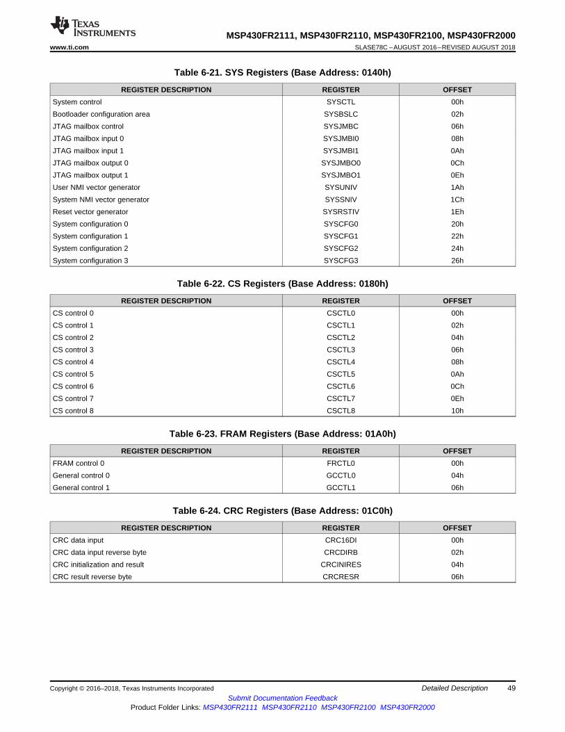
49
MSP430FR2111, MSP430FR2110, MSP430FR2100, MSP430FR2000www.ti.com SLASE78C –AUGUST 2016–REVISED AUGUST 2018
Submit Documentation FeedbackProduct Folder Links: MSP430FR2111 MSP430FR2110 MSP430FR2100 MSP430FR2000
Detailed DescriptionCopyright © 2016–2018, Texas Instruments Incorporated
Table 6-21. SYS Registers (Base Address: 0140h)
REGISTER DESCRIPTION REGISTER OFFSETSystem control SYSCTL 00hBootloader configuration area SYSBSLC 02hJTAG mailbox control SYSJMBC 06hJTAG mailbox input 0 SYSJMBI0 08hJTAG mailbox input 1 SYSJMBI1 0AhJTAG mailbox output 0 SYSJMBO0 0ChJTAG mailbox output 1 SYSJMBO1 0EhUser NMI vector generator SYSUNIV 1AhSystem NMI vector generator SYSSNIV 1ChReset vector generator SYSRSTIV 1EhSystem configuration 0 SYSCFG0 20hSystem configuration 1 SYSCFG1 22hSystem configuration 2 SYSCFG2 24hSystem configuration 3 SYSCFG3 26h
Table 6-22. CS Registers (Base Address: 0180h)
REGISTER DESCRIPTION REGISTER OFFSETCS control 0 CSCTL0 00hCS control 1 CSCTL1 02hCS control 2 CSCTL2 04hCS control 3 CSCTL3 06hCS control 4 CSCTL4 08hCS control 5 CSCTL5 0AhCS control 6 CSCTL6 0ChCS control 7 CSCTL7 0EhCS control 8 CSCTL8 10h
Table 6-23. FRAM Registers (Base Address: 01A0h)
REGISTER DESCRIPTION REGISTER OFFSETFRAM control 0 FRCTL0 00hGeneral control 0 GCCTL0 04hGeneral control 1 GCCTL1 06h
Table 6-24. CRC Registers (Base Address: 01C0h)
REGISTER DESCRIPTION REGISTER OFFSETCRC data input CRC16DI 00hCRC data input reverse byte CRCDIRB 02hCRC initialization and result CRCINIRES 04hCRC result reverse byte CRCRESR 06h

50
MSP430FR2111, MSP430FR2110, MSP430FR2100, MSP430FR2000SLASE78C –AUGUST 2016–REVISED AUGUST 2018 www.ti.com
Submit Documentation FeedbackProduct Folder Links: MSP430FR2111 MSP430FR2110 MSP430FR2100 MSP430FR2000
Detailed Description Copyright © 2016–2018, Texas Instruments Incorporated
Table 6-25. WDT Registers (Base Address: 01CCh)
REGISTER DESCRIPTION REGISTER OFFSETWatchdog timer control WDTCTL 00h
Table 6-26. Port P1, P2 Registers (Base Address: 0200h)
REGISTER DESCRIPTION REGISTER OFFSETPort P1 input P1IN 00hPort P1 output P1OUT 02hPort P1 direction P1DIR 04hPort P1 pulling enable P1REN 06hPort P1 selection 0 P1SEL0 0AhPort P1 selection 1 P1SEL1 0ChPort P1 interrupt vector word P1IV 0EhPort P1 interrupt edge select P1IES 18hPort P1 interrupt enable P1IE 1AhPort P1 interrupt flag P1IFG 1ChPort P2 input P2IN 01hPort P2 output P2OUT 03hPort P2 direction P2DIR 05hPort P2 pulling enable P2REN 07hPort P2 selection 0 P2SEL0 0BhPort P2 selection 1 P2SEL1 0DhPort P2 interrupt vector word P2IV 1EhPort P2 interrupt edge select P2IES 19hPort P2 interrupt enable P2IE 1BhPort P2 interrupt flag P2IFG 1Dh
Table 6-27. Capacitive Touch I/O Registers (Base Address: 02E0h)
REGISTER DESCRIPTION REGISTER OFFSETCapacitive Touch I/O 0 control CAPIO0CTL 0Eh
Table 6-28. RTC Registers (Base Address: 0300h)
REGISTER DESCRIPTION REGISTER OFFSETRTC control RTCCTL 00hRTC interrupt vector RTCIV 04hRTC modulo RTCMOD 08hRTC counter RTCCNT 0Ch
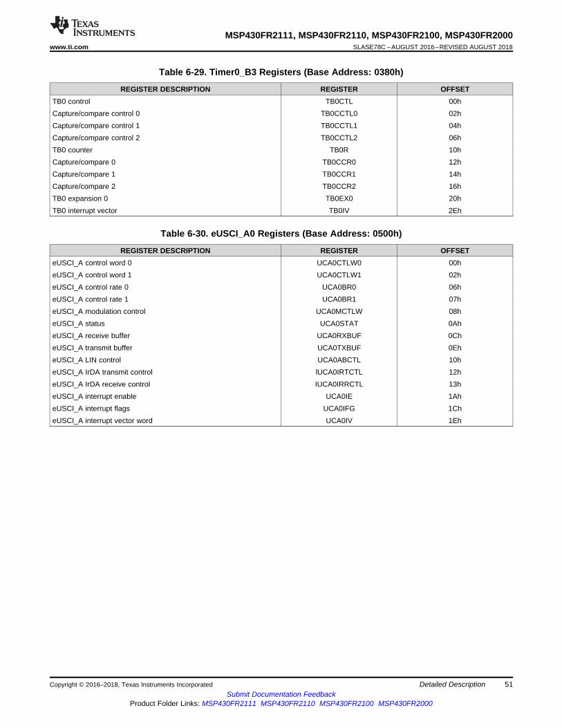
51
MSP430FR2111, MSP430FR2110, MSP430FR2100, MSP430FR2000www.ti.com SLASE78C –AUGUST 2016–REVISED AUGUST 2018
Submit Documentation FeedbackProduct Folder Links: MSP430FR2111 MSP430FR2110 MSP430FR2100 MSP430FR2000
Detailed DescriptionCopyright © 2016–2018, Texas Instruments Incorporated
Table 6-29. Timer0_B3 Registers (Base Address: 0380h)
REGISTER DESCRIPTION REGISTER OFFSETTB0 control TB0CTL 00hCapture/compare control 0 TB0CCTL0 02hCapture/compare control 1 TB0CCTL1 04hCapture/compare control 2 TB0CCTL2 06hTB0 counter TB0R 10hCapture/compare 0 TB0CCR0 12hCapture/compare 1 TB0CCR1 14hCapture/compare 2 TB0CCR2 16hTB0 expansion 0 TB0EX0 20hTB0 interrupt vector TB0IV 2Eh
Table 6-30. eUSCI_A0 Registers (Base Address: 0500h)
REGISTER DESCRIPTION REGISTER OFFSETeUSCI_A control word 0 UCA0CTLW0 00heUSCI_A control word 1 UCA0CTLW1 02heUSCI_A control rate 0 UCA0BR0 06heUSCI_A control rate 1 UCA0BR1 07heUSCI_A modulation control UCA0MCTLW 08heUSCI_A status UCA0STAT 0AheUSCI_A receive buffer UCA0RXBUF 0CheUSCI_A transmit buffer UCA0TXBUF 0EheUSCI_A LIN control UCA0ABCTL 10heUSCI_A IrDA transmit control lUCA0IRTCTL 12heUSCI_A IrDA receive control IUCA0IRRCTL 13heUSCI_A interrupt enable UCA0IE 1AheUSCI_A interrupt flags UCA0IFG 1CheUSCI_A interrupt vector word UCA0IV 1Eh

52
MSP430FR2111, MSP430FR2110, MSP430FR2100, MSP430FR2000SLASE78C –AUGUST 2016–REVISED AUGUST 2018 www.ti.com
Submit Documentation FeedbackProduct Folder Links: MSP430FR2111 MSP430FR2110 MSP430FR2100 MSP430FR2000
Detailed Description Copyright © 2016–2018, Texas Instruments Incorporated
Table 6-31. Backup Memory Registers (Base Address: 0660h)
REGISTER DESCRIPTION REGISTER OFFSETBackup memory 0 BAKMEM0 00hBackup memory 1 BAKMEM1 02hBackup memory 2 BAKMEM2 04hBackup memory 3 BAKMEM3 06hBackup memory 4 BAKMEM4 08hBackup memory 5 BAKMEM5 0AhBackup memory 6 BAKMEM6 0ChBackup memory 7 BAKMEM7 0EhBackup memory 8 BAKMEM8 10hBackup memory 9 BAKMEM9 12hBackup memory 10 BAKMEM10 14hBackup memory 11 BAKMEM11 16hBackup memory 12 BAKMEM12 18hBackup memory 13 BAKMEM13 1AhBackup memory 14 BAKMEM14 1ChBackup memory 15 BAKMEM15 1Eh
Table 6-32. ADC Registers (Base Address: 0700h)
REGISTER DESCRIPTION REGISTER OFFSETADC control 0 ADCCTL0 00hADC control 1 ADCCTL1 02hADC control 2 ADCCTL2 04hADC window comparator low threshold ADCLO 06hADC window comparator high threshold ADCHI 08hADC memory control 0 ADCMCTL0 0AhADC conversion memory ADCMEM0 12hADC interrupt enable ADCIE 1AhADC interrupt flags ADCIFG 1ChADC interrupt vector word ADCIV 1Eh
Table 6-33. eCOMP0 Registers (Base Address: 08E0h)
REGISTER DESCRIPTION REGISTER OFFSETComparator control 0 CPCTL0 00hComparator control 1 CPCTL1 02hComparator interrupt CPINT 06hComparator interrupt vector CPIV 08hComparator built-in DAC control CPDACCTL 10hComparator built-in DAC data CPDACDATA 12h
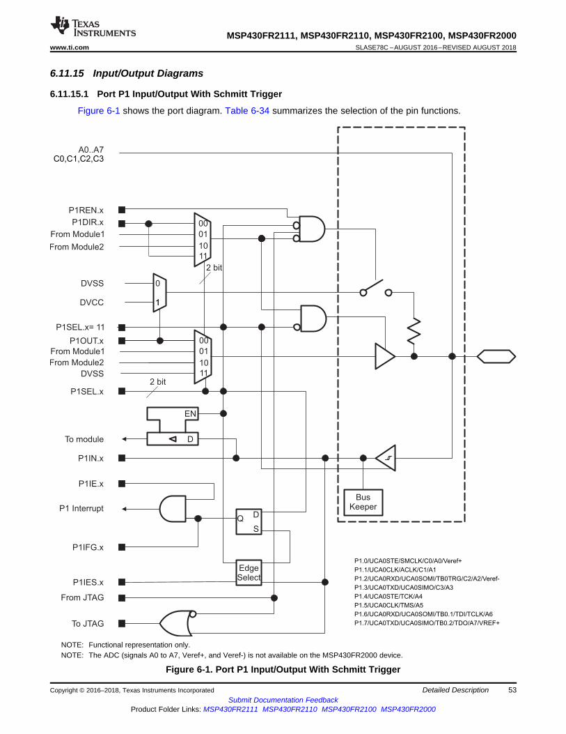
Q
0
1
D
S
EdgeSelect
P1IES.x
P1IFG.x
P1 Interrupt
P1IE.x
P1IN.x
To module
P1SEL.x
From Module1
P1OUT.x
P1DIR.x
11
From Module1
DVCC
DVSS
P1REN.x
EN
D
BusKeeper
From JTAG
To JTAG
2 bit
2 bit
10
01
00
11
10
01
00
From Module2
DVSS
From Module2
C0,C1,C2,C3A0..A7
P1.5/ /TMS/A5UCA0CLK
P1.4/ /TCK/A4UCA0STE
P1.6/ /TB0.1/TDI/TCLK/A6UCA0RXD/UCA0SOMI
P1.7/ /TB0.2/TDO/A7UCA0TXD/UCA0SIMO /VREF+
P1.1/UCA0CLK/ACLK/C1/A1
P1.0/UCA0STE/SMCLK/C0/A0/Veref+
P1.3/UCA0TXD/UCA0SIMO/C3/A3
P1.2/UCA0RXD/UCA0SOMI/ A2/Veref-TB0TRG/C2/
1
P1SEL.x= 11
53
MSP430FR2111, MSP430FR2110, MSP430FR2100, MSP430FR2000www.ti.com SLASE78C –AUGUST 2016–REVISED AUGUST 2018
Submit Documentation FeedbackProduct Folder Links: MSP430FR2111 MSP430FR2110 MSP430FR2100 MSP430FR2000
Detailed DescriptionCopyright © 2016–2018, Texas Instruments Incorporated
6.11.15 Input/Output Diagrams
6.11.15.1 Port P1 Input/Output With Schmitt Trigger
Figure 6-1 shows the port diagram. Table 6-34 summarizes the selection of the pin functions.
NOTE: Functional representation only.NOTE: The ADC (signals A0 to A7, Veref+, and Veref-) is not available on the MSP430FR2000 device.
Figure 6-1. Port P1 Input/Output With Schmitt Trigger
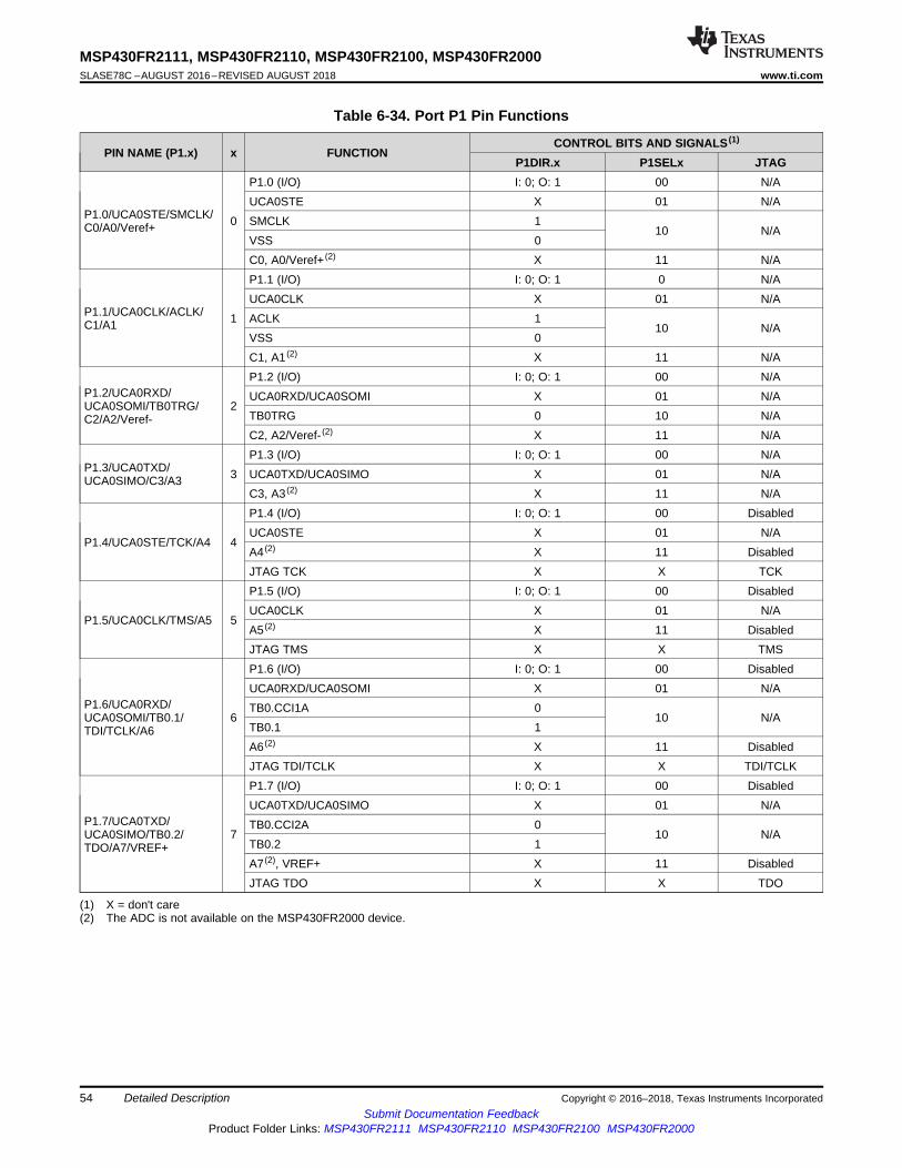
54
MSP430FR2111, MSP430FR2110, MSP430FR2100, MSP430FR2000SLASE78C –AUGUST 2016–REVISED AUGUST 2018 www.ti.com
Submit Documentation FeedbackProduct Folder Links: MSP430FR2111 MSP430FR2110 MSP430FR2100 MSP430FR2000
Detailed Description Copyright © 2016–2018, Texas Instruments Incorporated
(1) X = don't care(2) The ADC is not available on the MSP430FR2000 device.
Table 6-34. Port P1 Pin Functions
PIN NAME (P1.x) x FUNCTIONCONTROL BITS AND SIGNALS (1)
P1DIR.x P1SELx JTAG
P1.0/UCA0STE/SMCLK/C0/A0/Veref+ 0
P1.0 (I/O) I: 0; O: 1 00 N/AUCA0STE X 01 N/ASMCLK 1
10 N/AVSS 0C0, A0/Veref+ (2) X 11 N/A
P1.1/UCA0CLK/ACLK/C1/A1 1
P1.1 (I/O) I: 0; O: 1 0 N/AUCA0CLK X 01 N/AACLK 1
10 N/AVSS 0C1, A1 (2) X 11 N/A
P1.2/UCA0RXD/UCA0SOMI/TB0TRG/C2/A2/Veref-
2
P1.2 (I/O) I: 0; O: 1 00 N/AUCA0RXD/UCA0SOMI X 01 N/ATB0TRG 0 10 N/AC2, A2/Veref- (2) X 11 N/A
P1.3/UCA0TXD/UCA0SIMO/C3/A3 3
P1.3 (I/O) I: 0; O: 1 00 N/AUCA0TXD/UCA0SIMO X 01 N/AC3, A3 (2) X 11 N/A
P1.4/UCA0STE/TCK/A4 4
P1.4 (I/O) I: 0; O: 1 00 DisabledUCA0STE X 01 N/AA4 (2) X 11 DisabledJTAG TCK X X TCK
P1.5/UCA0CLK/TMS/A5 5
P1.5 (I/O) I: 0; O: 1 00 DisabledUCA0CLK X 01 N/AA5 (2) X 11 DisabledJTAG TMS X X TMS
P1.6/UCA0RXD/UCA0SOMI/TB0.1/TDI/TCLK/A6
6
P1.6 (I/O) I: 0; O: 1 00 DisabledUCA0RXD/UCA0SOMI X 01 N/ATB0.CCI1A 0
10 N/ATB0.1 1A6 (2) X 11 DisabledJTAG TDI/TCLK X X TDI/TCLK
P1.7/UCA0TXD/UCA0SIMO/TB0.2/TDO/A7/VREF+
7
P1.7 (I/O) I: 0; O: 1 00 DisabledUCA0TXD/UCA0SIMO X 01 N/ATB0.CCI2A 0
10 N/ATB0.2 1A7 (2), VREF+ X 11 DisabledJTAG TDO X X TDO
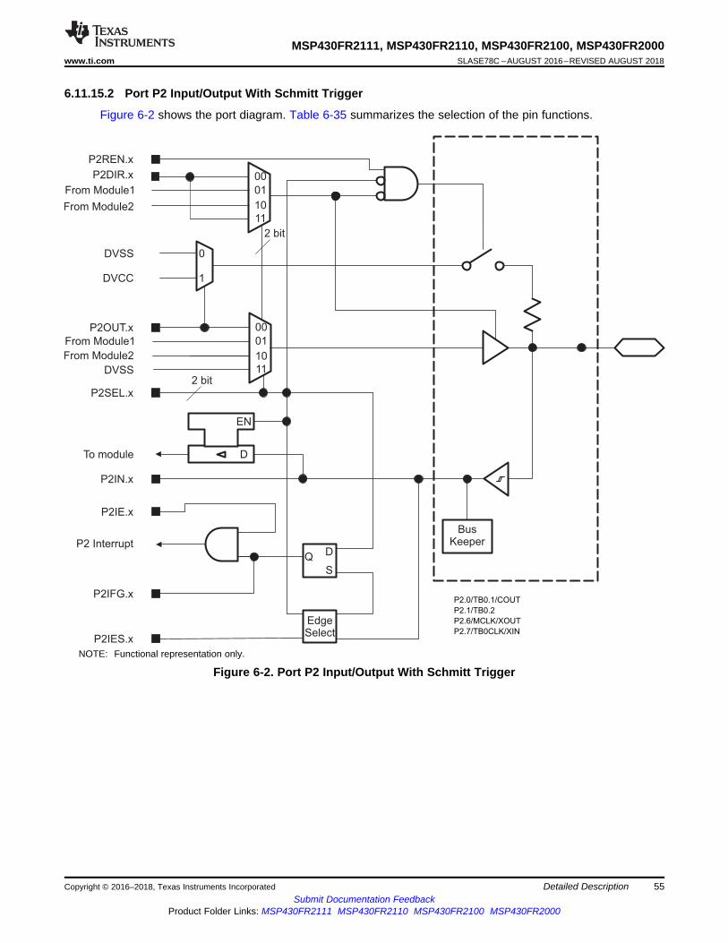
0
1
To module
P2SEL.x
From Module1
P2OUT.x
P2DIR.x
11
From Module1
DVCC
DVSS
P2REN.x
EN
D
2 bit
2 bit
10
01
00
11
10
01
00
From Module2
DVSS
From Module2
P2.1/TB0.2
P2.0/TB0.1/COUT
P2.6/MCLK/XOUT
P2.7/TB0CLK/XIN
Q D
S
EdgeSelect
P2IES.x
P2IFG.x
P2 Interrupt
P2IE.x
P2IN.x
BusKeeper
55
MSP430FR2111, MSP430FR2110, MSP430FR2100, MSP430FR2000www.ti.com SLASE78C –AUGUST 2016–REVISED AUGUST 2018
Submit Documentation FeedbackProduct Folder Links: MSP430FR2111 MSP430FR2110 MSP430FR2100 MSP430FR2000
Detailed DescriptionCopyright © 2016–2018, Texas Instruments Incorporated
6.11.15.2 Port P2 Input/Output With Schmitt Trigger
Figure 6-2 shows the port diagram. Table 6-35 summarizes the selection of the pin functions.
NOTE: Functional representation only.
Figure 6-2. Port P2 Input/Output With Schmitt Trigger
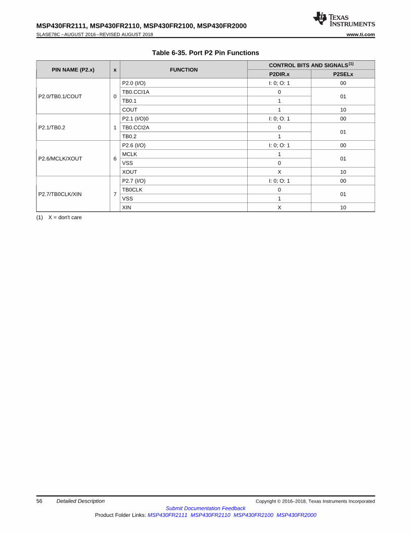
56
MSP430FR2111, MSP430FR2110, MSP430FR2100, MSP430FR2000SLASE78C –AUGUST 2016–REVISED AUGUST 2018 www.ti.com
Submit Documentation FeedbackProduct Folder Links: MSP430FR2111 MSP430FR2110 MSP430FR2100 MSP430FR2000
Detailed Description Copyright © 2016–2018, Texas Instruments Incorporated
(1) X = don't care
Table 6-35. Port P2 Pin Functions
PIN NAME (P2.x) x FUNCTIONCONTROL BITS AND SIGNALS (1)
P2DIR.x P2SELx
P2.0/TB0.1/COUT 0
P2.0 (I/O) I: 0; O: 1 00TB0.CCI1A 0
01TB0.1 1COUT 1 10
P2.1/TB0.2 1P2.1 (I/O)0 I: 0; O: 1 00TB0.CCI2A 0
01TB0.2 1
P2.6/MCLK/XOUT 6
P2.6 (I/O) I: 0; O: 1 00MCLK 1
01VSS 0XOUT X 10
P2.7/TB0CLK/XIN 7
P2.7 (I/O) I: 0; O: 1 00TB0CLK 0
01VSS 1XIN X 10
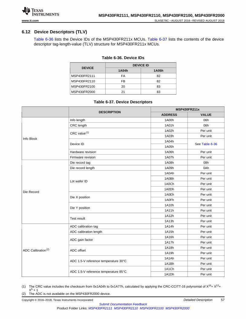
57
MSP430FR2111, MSP430FR2110, MSP430FR2100, MSP430FR2000www.ti.com SLASE78C –AUGUST 2016–REVISED AUGUST 2018
Submit Documentation FeedbackProduct Folder Links: MSP430FR2111 MSP430FR2110 MSP430FR2100 MSP430FR2000
Detailed DescriptionCopyright © 2016–2018, Texas Instruments Incorporated
6.12 Device Descriptors (TLV)Table 6-36 lists the Device IDs of the MSP430FR211x MCUs. Table 6-37 lists the contents of the devicedescriptor tag-length-value (TLV) structure for MSP430FR211x MCUs.
Table 6-36. Device IDs
DEVICEDEVICE ID
1A04h 1A05hMSP430FR2111 FA 82MSP430FR2110 FB 82MSP430FR2100 20 83MSP430FR2000 21 83
(1) The CRC value includes the checksum from 0x1A04h to 0x1A77h, calculated by applying the CRC-CCITT-16 polynomial of X16+ X12+X5 + 1
(2) The ADC is not available on the MSP430FR2000 device.
Table 6-37. Device Descriptors
DESCRIPTIONMSP430FR211x
ADDRESS VALUE
Info Block
Info length 1A00h 06hCRC length 1A01h 06h
CRC value (1) 1A02h Per unit1A03h Per unit
Device ID1A04h
See Table 6-361A05h
Hardware revision 1A06h Per unitFirmware revision 1A07h Per unit
Die Record
Die record tag 1A08h 08hDie record length 1A09h 0Ah
Lot wafer ID
1A0Ah Per unit1A0Bh Per unit1A0Ch Per unit1A0Dh Per unit
Die X position1A0Eh Per unit1A0Fh Per unit
Die Y position1A10h Per unit1A11h Per unit
Test result1A12h Per unit1A13h Per unit
ADC Calibration (2)
ADC calibration tag 1A14h Per unitADC calibration length 1A15h Per unit
ADC gain factor1A16h Per unit1A17h Per unit
ADC offset1A18h Per unit1A19h Per unit
ADC 1.5-V reference temperature 30°C1A1Ah Per unit1A1Bh Per unit
ADC 1.5-V reference temperature 85°C1A1Ch Per unit1A1Dh Per unit

58
MSP430FR2111, MSP430FR2110, MSP430FR2100, MSP430FR2000SLASE78C –AUGUST 2016–REVISED AUGUST 2018 www.ti.com
Submit Documentation FeedbackProduct Folder Links: MSP430FR2111 MSP430FR2110 MSP430FR2100 MSP430FR2000
Detailed Description Copyright © 2016–2018, Texas Instruments Incorporated
Table 6-37. Device Descriptors (continued)
DESCRIPTIONMSP430FR211x
ADDRESS VALUE
(3) This value can be directly loaded into the DCO bits in the CSCTL0 register to get accurate 16-MHz frequence at room temperature,especially when the MCU exits from LPM3 and below. TI suggests using a predivider to decrease the frequency if the temperature driftmight result an overshoot >16 MHz.
Reference and DCOCalibration
Calibration tag 1A1Eh 12hCalibration length 1A1Fh 04h
1.5-V reference factor1A20h Per unit1A21h Per unit
DCO tap settings for 16 MHz, temperature 30°C (3) 1A22h Per unit1A23h Per unit
6.13 Identification
6.13.1 Revision IdentificationThe device revision information is shown as part of the top-side marking on the device package. Thedevice-specific errata sheet describes these markings. For links to the errata sheets for the devices in thisdata sheet, see Section 8.4.
The hardware revision is also stored in the Device Descriptor structure in the Info Block section. Fordetails on this value, see the "Hardware Revision" entries in Section 6.12.
6.13.2 Device IdentificationThe device type can be identified from the top-side marking on the device package. The device-specificerrata sheet describes these markings. For links to the errata sheets for the devices in this data sheet, seeSection 8.4.
A device identification value is also stored in the Device Descriptor structure in the Info Block section. Fordetails on this value, see the "Device ID" entries in Section 6.12.
6.13.3 JTAG IdentificationProgramming through the JTAG interface, including reading and identifying the JTAG ID, is described indetail in MSP430 Programming With the JTAG Interface.
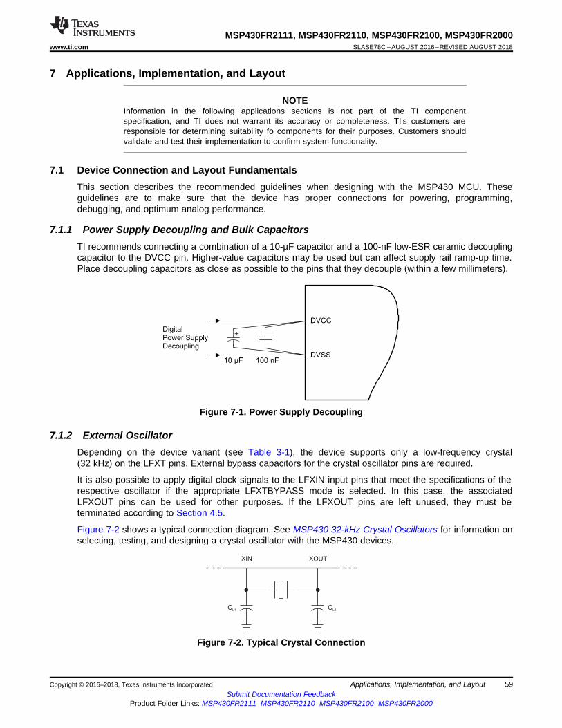
CL1
CL2
XIN XOUT
DigitalPower SupplyDecoupling
100 nF10 µF
DVCC
DVSS
+
59
MSP430FR2111, MSP430FR2110, MSP430FR2100, MSP430FR2000www.ti.com SLASE78C –AUGUST 2016–REVISED AUGUST 2018
Submit Documentation FeedbackProduct Folder Links: MSP430FR2111 MSP430FR2110 MSP430FR2100 MSP430FR2000
Applications, Implementation, and LayoutCopyright © 2016–2018, Texas Instruments Incorporated
7 Applications, Implementation, and Layout
NOTEInformation in the following applications sections is not part of the TI componentspecification, and TI does not warrant its accuracy or completeness. TI's customers areresponsible for determining suitability fo components for their purposes. Customers shouldvalidate and test their implementation to confirm system functionality.
7.1 Device Connection and Layout FundamentalsThis section describes the recommended guidelines when designing with the MSP430 MCU. Theseguidelines are to make sure that the device has proper connections for powering, programming,debugging, and optimum analog performance.
7.1.1 Power Supply Decoupling and Bulk CapacitorsTI recommends connecting a combination of a 10-µF capacitor and a 100-nF low-ESR ceramic decouplingcapacitor to the DVCC pin. Higher-value capacitors may be used but can affect supply rail ramp-up time.Place decoupling capacitors as close as possible to the pins that they decouple (within a few millimeters).
Figure 7-1. Power Supply Decoupling
7.1.2 External OscillatorDepending on the device variant (see Table 3-1), the device supports only a low-frequency crystal(32 kHz) on the LFXT pins. External bypass capacitors for the crystal oscillator pins are required.
It is also possible to apply digital clock signals to the LFXIN input pins that meet the specifications of therespective oscillator if the appropriate LFXTBYPASS mode is selected. In this case, the associatedLFXOUT pins can be used for other purposes. If the LFXOUT pins are left unused, they must beterminated according to Section 4.5.
Figure 7-2 shows a typical connection diagram. See MSP430 32-kHz Crystal Oscillators for information onselecting, testing, and designing a crystal oscillator with the MSP430 devices.
Figure 7-2. Typical Crystal Connection
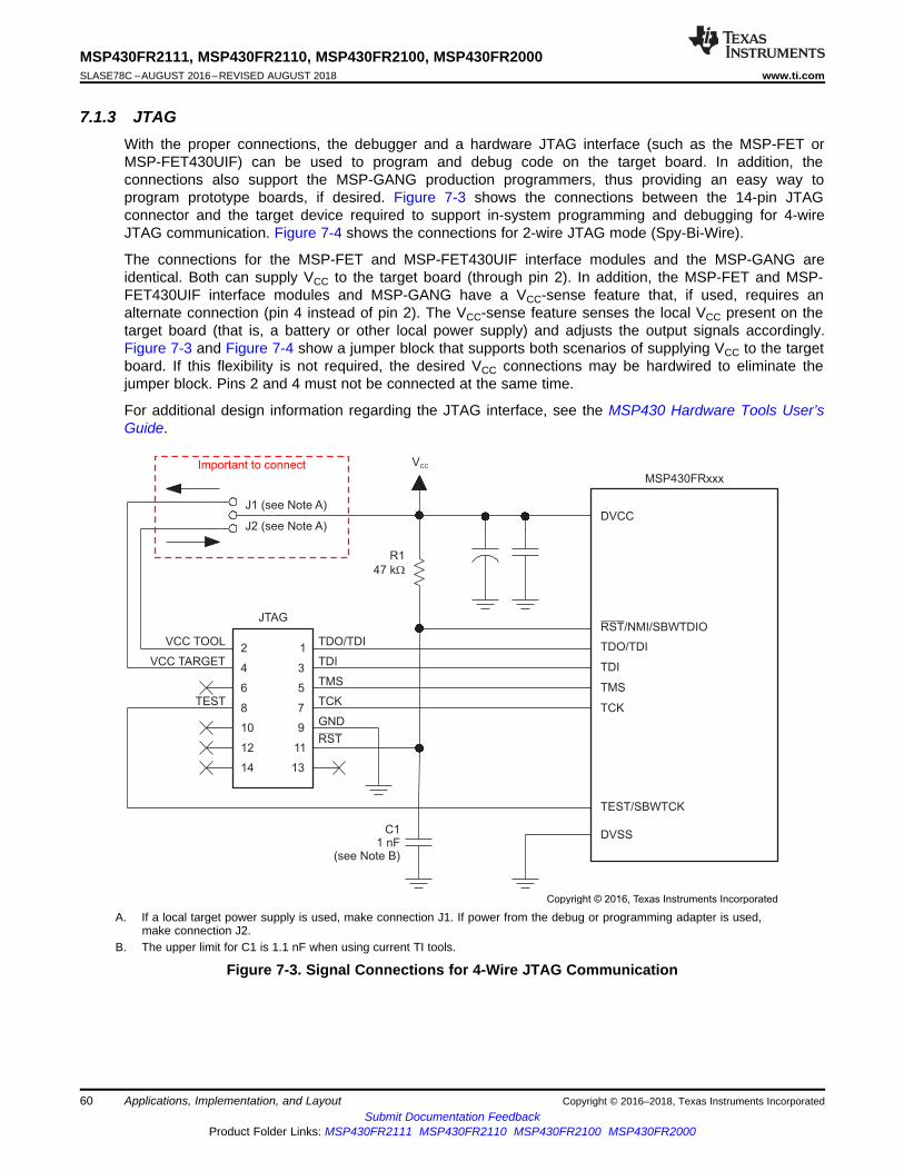
1
3
5
7
9
11
13
2
4
6
8
10
12
14
TDO/TDI
TDI
TMS
TCK
GND
TEST
JTAG
VCC TOOL
VCC TARGET
J1 (see Note A)
J2 (see Note A)
VCC
R1
47 kW
DVCC
RST/NMI/SBWTDIO
TDO/TDI
TDI
TMS
TCK
TEST/SBWTCK
DVSS
MSP430FRxxx
C11 nF
(see Note B)
RST
Important to connect
Copyright © 2016, Texas Instruments Incorporated
60
MSP430FR2111, MSP430FR2110, MSP430FR2100, MSP430FR2000SLASE78C –AUGUST 2016–REVISED AUGUST 2018 www.ti.com
Submit Documentation FeedbackProduct Folder Links: MSP430FR2111 MSP430FR2110 MSP430FR2100 MSP430FR2000
Applications, Implementation, and Layout Copyright © 2016–2018, Texas Instruments Incorporated
7.1.3 JTAGWith the proper connections, the debugger and a hardware JTAG interface (such as the MSP-FET orMSP-FET430UIF) can be used to program and debug code on the target board. In addition, theconnections also support the MSP-GANG production programmers, thus providing an easy way toprogram prototype boards, if desired. Figure 7-3 shows the connections between the 14-pin JTAGconnector and the target device required to support in-system programming and debugging for 4-wireJTAG communication. Figure 7-4 shows the connections for 2-wire JTAG mode (Spy-Bi-Wire).
The connections for the MSP-FET and MSP-FET430UIF interface modules and the MSP-GANG areidentical. Both can supply VCC to the target board (through pin 2). In addition, the MSP-FET and MSP-FET430UIF interface modules and MSP-GANG have a VCC-sense feature that, if used, requires analternate connection (pin 4 instead of pin 2). The VCC-sense feature senses the local VCC present on thetarget board (that is, a battery or other local power supply) and adjusts the output signals accordingly.Figure 7-3 and Figure 7-4 show a jumper block that supports both scenarios of supplying VCC to the targetboard. If this flexibility is not required, the desired VCC connections may be hardwired to eliminate thejumper block. Pins 2 and 4 must not be connected at the same time.
For additional design information regarding the JTAG interface, see the MSP430 Hardware Tools User’sGuide.
A. If a local target power supply is used, make connection J1. If power from the debug or programming adapter is used,make connection J2.
B. The upper limit for C1 is 1.1 nF when using current TI tools.
Figure 7-3. Signal Connections for 4-Wire JTAG Communication
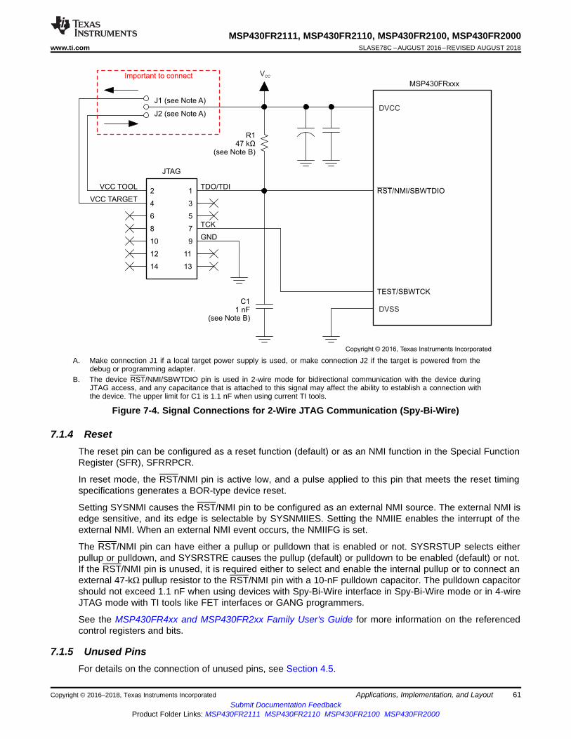
1
3
5
7
9
11
13
2
4
6
8
10
12
14
TEST/SBWTCK
MSP430FRxxx
RST/NMI/SBWTDIOTDO/TDI
TCK
GND
JTAG
R147 kΩ
(see Note B)
VCC TOOL
VCC TARGET
C11 nF
(see Note B)
J1 (see Note A)
J2 (see Note A)
Important to connect
DVCC
DVSS
VCC
Copyright © 2016, Texas Instruments Incorporated
61
MSP430FR2111, MSP430FR2110, MSP430FR2100, MSP430FR2000www.ti.com SLASE78C –AUGUST 2016–REVISED AUGUST 2018
Submit Documentation FeedbackProduct Folder Links: MSP430FR2111 MSP430FR2110 MSP430FR2100 MSP430FR2000
Applications, Implementation, and LayoutCopyright © 2016–2018, Texas Instruments Incorporated
A. Make connection J1 if a local target power supply is used, or make connection J2 if the target is powered from thedebug or programming adapter.
B. The device RST/NMI/SBWTDIO pin is used in 2-wire mode for bidirectional communication with the device duringJTAG access, and any capacitance that is attached to this signal may affect the ability to establish a connection withthe device. The upper limit for C1 is 1.1 nF when using current TI tools.
Figure 7-4. Signal Connections for 2-Wire JTAG Communication (Spy-Bi-Wire)
7.1.4 ResetThe reset pin can be configured as a reset function (default) or as an NMI function in the Special FunctionRegister (SFR), SFRRPCR.
In reset mode, the RST/NMI pin is active low, and a pulse applied to this pin that meets the reset timingspecifications generates a BOR-type device reset.
Setting SYSNMI causes the RST/NMI pin to be configured as an external NMI source. The external NMI isedge sensitive, and its edge is selectable by SYSNMIIES. Setting the NMIIE enables the interrupt of theexternal NMI. When an external NMI event occurs, the NMIIFG is set.
The RST/NMI pin can have either a pullup or pulldown that is enabled or not. SYSRSTUP selects eitherpullup or pulldown, and SYSRSTRE causes the pullup (default) or pulldown to be enabled (default) or not.If the RST/NMI pin is unused, it is required either to select and enable the internal pullup or to connect anexternal 47-kΩ pullup resistor to the RST/NMI pin with a 10-nF pulldown capacitor. The pulldown capacitorshould not exceed 1.1 nF when using devices with Spy-Bi-Wire interface in Spy-Bi-Wire mode or in 4-wireJTAG mode with TI tools like FET interfaces or GANG programmers.
See the MSP430FR4xx and MSP430FR2xx Family User's Guide for more information on the referencedcontrol registers and bits.
7.1.5 Unused PinsFor details on the connection of unused pins, see Section 4.5.
Using an externalpositive reference
Using an externalnegative reference VEREF-
VREF+/VEREF+
+
+
100 nF10 Fµ
100 nF10 Fµ
DVSS
62
MSP430FR2111, MSP430FR2110, MSP430FR2100, MSP430FR2000SLASE78C –AUGUST 2016–REVISED AUGUST 2018 www.ti.com
Submit Documentation FeedbackProduct Folder Links: MSP430FR2111 MSP430FR2110 MSP430FR2100 MSP430FR2000
Applications, Implementation, and Layout Copyright © 2016–2018, Texas Instruments Incorporated
7.1.6 General Layout Recommendations• Proper grounding and short traces for external crystal to reduce parasitic capacitance. See MSP430
32-kHz Crystal Oscillators for recommended layout guidelines.• Proper bypass capacitors on DVCC, AVCC, and reference pins if used.• Avoid routing any high-frequency signal close to an analog signal line. For example, keep digital
switching signals such as PWM or JTAG signals away from the oscillator circuit and ADC signals.• Proper ESD level protection should be considered to protect the device from unintended high-voltage
electrostatic discharge. See MSP430 System-Level ESD Considerations for guidelines.
7.1.7 Do's and Don'tsDuring power up, power down, and device operation, the voltage difference between AVCC and DVCCmust not exceed the limits specified in Absolute Maximum Ratings. Exceeding the specified limits maycause malfunction of the device including erroneous writes to RAM and FRAM.
7.2 Peripheral- and Interface-Specific Design Information
7.2.1 ADC Peripheral
NOTEThe ADC is not available on the MSP430FR2000 device.
7.2.1.1 Partial Schematic
Figure 7-5 shows the recommended decoupling circuit with either an internal or an external voltagereference.
Figure 7-5. ADC Grounding and Noise Considerations
7.2.1.2 Design Requirements
As with any high-resolution ADC, appropriate printed-circuit-board layout and grounding techniques shouldbe followed to eliminate ground loops, unwanted parasitic effects, and noise.
Ground loops are formed when return current from the ADC flows through paths that are common withother analog or digital circuitry. If care is not taken, this current can generate small unwanted offsetvoltages that can add to or subtract from the reference or input voltages of the ADC. The generalguidelines in Section 7.1.1 combined with the connections shown in Section 7.2.1.1 prevent this.
In addition to grounding, ripple and noise spikes on the power-supply lines that are caused by digitalswitching or switching power supplies can corrupt the conversion result. TI recommends a noise-freedesign using separate analog and digital ground planes with a single-point connection to achieve highaccuracy.
63
MSP430FR2111, MSP430FR2110, MSP430FR2100, MSP430FR2000www.ti.com SLASE78C –AUGUST 2016–REVISED AUGUST 2018
Submit Documentation FeedbackProduct Folder Links: MSP430FR2111 MSP430FR2110 MSP430FR2100 MSP430FR2000
Applications, Implementation, and LayoutCopyright © 2016–2018, Texas Instruments Incorporated
Figure 7-5 shows the recommended decoupling circuit when an external voltage reference is used. Theinternal reference module has a maximum drive current as described in the sections ADC Pin Enable and1.2-V Reference Settings of the MSP430FR4xx and MSP430FR2xx Family User's Guide.
The reference voltage must be a stable voltage for accurate measurements. The capacitor values that areselected in the general guidelines filter out the high- and low-frequency ripple before the reference voltageenters the device. In this case, the 10-µF capacitor is used to buffer the reference pin and filter any low-frequency ripple. A bypass capacitor of 100 nF is used to filter out any high-frequency noise.
7.2.1.3 Layout Guidelines
Components that are shown in the partial schematic (see Figure 7-5) should be placed as close aspossible to the respective device pins to avoid long traces, because they add additional parasiticcapacitance, inductance, and resistance on the signal.
Avoid routing analog input signals close to a high-frequency pin (for example, a high-frequency PWM),because the high-frequency switching can be coupled into the analog signal.
7.3 Typical ApplicationsTable 7-1 lists several TI Designs that reflect the use of the MSP430FR211x family of devices in differentreal-world application scenarios. Consult these designs for additional guidance regarding schematic,layout, and software implementation. For the most up-to-date list of available TI Designs, see the device-specific product folders listed in Section 8.5.
Table 7-1. TI Designs
DESIGN NAME LINKThermostat Implementation With MSP430FR4xx TIDM-FRAM-THERMOSTATWater Meter Implementation With MSP430FR4xx TIDM-FRAM-WATERMETERRemote Controller of Air Conditioner Using Low-Power Microcontroller TIDM-REMOTE-CONTROLLER-FOR-AC
MSP 430 FR 2 111 I PW R
Processor Family
Series
PackagingMCU Platform
Distribution Format
Memory Type Temperature Range
Feature Set
Processor Family MSP = Mixed-Signal ProcessorXMS = Experimental Silicon
MCU Platform 430 = TI’s 16-bit MSP430 Low-Power Microcontroller Platform
Memory Type
Series
Feature Set
Temperature Range
FR = FRAM
2 = FRAM 2 Series up to 16 MHz without LCD
Variations of the device features; see the Device Comparison section for details
I = –40 C to 85 C° °
Packaging www.ti.com/packaging
Distribution Format T = Small reelR = Large reelNo marking = Tube or tray
64
MSP430FR2111, MSP430FR2110, MSP430FR2100, MSP430FR2000SLASE78C –AUGUST 2016–REVISED AUGUST 2018 www.ti.com
Submit Documentation FeedbackProduct Folder Links: MSP430FR2111 MSP430FR2110 MSP430FR2100 MSP430FR2000
Device and Documentation Support Copyright © 2016–2018, Texas Instruments Incorporated
8 Device and Documentation Support
8.1 Getting Started and Next StepsFor more information on the MSP430™ family of devices and the tools and libraries that are available tohelp with your development, visit the Getting Started page.
8.2 Device NomenclatureTo designate the stages in the product development cycle, TI assigns prefixes to the part numbers of allMSP MCU devices. Each MSP MCU commercial family member has one of two prefixes: MSP or XMS.These prefixes represent evolutionary stages of product development from engineering prototypes (XMS)through fully qualified production devices (MSP).
XMS – Experimental device that is not necessarily representative of the final device's electricalspecifications
MSP – Fully qualified production device
XMS devices are shipped against the following disclaimer:
"Developmental product is intended for internal evaluation purposes."
MSP devices have been characterized fully, and the quality and reliability of the device have beendemonstrated fully. TI's standard warranty applies.
Predictions show that prototype devices (XMS) have a greater failure rate than the standard productiondevices. TI recommends that these devices not be used in any production system because their expectedend-use failure rate still is undefined. Only qualified production devices are to be used.
TI device nomenclature also includes a suffix with the device family name. This suffix indicates thetemperature range, package type, and distribution format. Figure 8-1 provides a legend for reading thecomplete device name.
Figure 8-1. Device Nomenclature
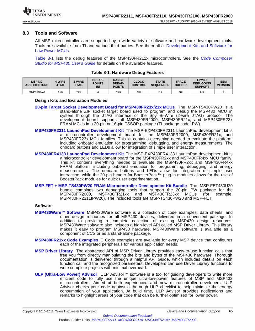
65
MSP430FR2111, MSP430FR2110, MSP430FR2100, MSP430FR2000www.ti.com SLASE78C –AUGUST 2016–REVISED AUGUST 2018
Submit Documentation FeedbackProduct Folder Links: MSP430FR2111 MSP430FR2110 MSP430FR2100 MSP430FR2000
Device and Documentation SupportCopyright © 2016–2018, Texas Instruments Incorporated
8.3 Tools and SoftwareAll MSP microcontrollers are supported by a wide variety of software and hardware development tools.Tools are available from TI and various third parties. See them all at Development Kits and Software forLow-Power MCUs.
Table 8-1 lists the debug features of the MSP430FR211x microcontrollers. See the Code ComposerStudio for MSP430 User's Guide for details on the available features.
Table 8-1. Hardware Debug Features
MSP430ARCHITECTURE
4-WIREJTAG
2-WIREJTAG
BREAK-POINTS
(N)
RANGEBREAK-POINTS
CLOCKCONTROL
STATESEQUENCER
TRACEBUFFER
LPMx.5DEBUGGING
SUPPORTEEM
VERSION
MSP430Xv2 Yes Yes 3 Yes Yes No No No S
Design Kits and Evaluation Modules20-pin Target Socket Development Board for MSP430FR23x/21x MCUs The MSP-TS430PW20 is a
stand-alone ZIF socket target board used to program and debug the MSP430 MCU insystem through the JTAG interface or the Spy Bi-Wire (2-wire JTAG) protocol. Thedevelopment board supports all MSP430FR2000, MSP430FR21x, and MSP430FR23xFRAM MCUs in a 20-pin or 16-pin TSSOP package (TI package code: PW).
MSP430FR2311 LaunchPad Development Kit The MSP-EXP430FR2311 LaunchPad development kit isa microcontroller development board for the MSP430FR2000, MSP430FR21x, andMSP430FR23x MCU families. This kit contains everything needed to evaluate the platform,including onboard emulation for programming, debugging, and energy measurements. Theonboard buttons and LEDs allow for integration of simple user interaction.
MSP430FR4133 LaunchPad Development Kit The MSP-EXP430FR4133 LaunchPad development kit isa microcontroller development board for the MSP430FR2xx and MSP430FR4xx MCU family.This kit contains everything needed to evaluate the MSP430FR2xx and MSP430FR4xxFRAM platform, including onboard emulation for programming, debugging, and energymeasurements. The onboard buttons and LEDs allow for integration of simple userinteraction, while the 20-pin header for BoosterPack™ plug-in modules allows for the use ofBoosterPack modules for quick user experimentation.
MSP-FET + MSP-TS430PW20 FRAM Microcontroller Development Kit Bundle The MSP-FET430U20bundle combines two debugging tools that support the 20-pin PW package for theMSP430FR2000, MSP430FR21xx and MSP430FR23xx MCUs (for example,MSP430FR2311IPW20). The included tools are MSP-TS430PW20 and MSP-FET.
SoftwareMSP430Ware™ Software MSP430Ware software is a collection of code examples, data sheets, and
other design resources for all MSP430 devices, delivered in a convenient package. Inaddition to providing a complete collection of existing MSP430 design resources,MSP430Ware software also includes a high-level API called MSP Driver Library. This librarymakes it easy to program MSP430 hardware. MSP430Ware software is available as acomponent of CCS or as a stand-alone package.
MSP430FR21xx Code Examples C Code examples are available for every MSP device that configureseach of the integrated peripherals for various application needs.
MSP Driver Library The abstracted API of MSP Driver Library provides easy-to-use function calls thatfree you from directly manipulating the bits and bytes of the MSP430 hardware. Thoroughdocumentation is delivered through a helpful API Guide, which includes details on eachfunction call and the recognized parameters. Developers can use Driver Library functions towrite complete projects with minimal overhead.
ULP (Ultra-Low Power) Advisor ULP Advisor™ software is a tool for guiding developers to write moreefficient code to fully use the unique ultra-low-power features of MSP and MSP432microcontrollers. Aimed at both experienced and new microcontroller developers, ULPAdvisor checks your code against a thorough ULP checklist to help minimize the energyconsumption of your application. At build time, ULP Advisor provides notifications andremarks to highlight areas of your code that can be further optimized for lower power.
66
MSP430FR2111, MSP430FR2110, MSP430FR2100, MSP430FR2000SLASE78C –AUGUST 2016–REVISED AUGUST 2018 www.ti.com
Submit Documentation FeedbackProduct Folder Links: MSP430FR2111 MSP430FR2110 MSP430FR2100 MSP430FR2000
Device and Documentation Support Copyright © 2016–2018, Texas Instruments Incorporated
IEC60730 Software Package The IEC60730 MSP430 software package was developed to helpcustomers comply with IEC 60730-1:2010 (Automatic Electrical Controls for Household andSimilar Use – Part 1: General Requirements) for up to Class B products, which includeshome appliances, arc detectors, power converters, power tools, e-bikes, and many others.The IEC60730 MSP430 software package can be embedded in customer applicationsrunning on MSP430s to help simplify the customer's certification efforts of functional safety-compliant consumer devices to IEC 60730-1:2010 Class B.
Fixed Point Math Library for MSP The MSP IQmath and Qmath Libraries are a collection of highlyoptimized and high-precision mathematical functions for C programmers to seamlessly port afloating-point algorithm into fixed-point code on MSP430 and MSP432 devices. Theseroutines are typically used in computationally intensive real-time applications where optimalexecution speed, high accuracy, and ultra-low energy are critical. By using the IQmath andQmath libraries, it is possible to achieve execution speeds considerably faster and energyconsumption considerably lower than equivalent code written using floating-point math.
Floating Point Math Library for MSP430 Continuing to innovate in the low-power and low-costmicrocontroller space, TI provides MSPMATHLIB. Leveraging the intelligent peripherals ofour devices, this floating-point math library of scalar functions that are up to 26 times fasterthan the standard MSP430 math functions. Mathlib is easy to integrate into your designs.This library is free and is integrated in both Code Composer Studio IDE and IAR EmbeddedWorkbench IDE.
Development ToolsCode Composer Studio™ Integrated Development Environment for MSP Microcontrollers Code
Composer Studio (CCS) integrated development environment (IDE) supports all MSPmicrocontroller devices. CCS comprises a suite of embedded software utilities used todevelop and debug embedded applications. It includes an optimizing C/C++ compiler, sourcecode editor, project build environment, debugger, profiler, and many other features.
MSP EnergyTrace™ Technology EnergyTrace technology for MSP430 microcontrollers is an energy-based code analysis tool that measures and displays the energy profile of the applicationand helps to optimize it for ultra-low-power consumption.
Command-Line Programmer MSP Flasher is an open-source shell-based interface for programmingMSP microcontrollers through a FET programmer or eZ430 using JTAG or Spy-Bi-Wire(SBW) communication. MSP Flasher can download binary files (.txt or .hex) directly to theMSP microcontroller without an IDE.
MSP MCU Programmer and Debugger The MSP-FET is a powerful emulation development tool – oftencalled a debug probe – which lets users quickly begin application development on MSP low-power MCUs. Creating MCU software usually requires downloading the resulting binaryprogram to the MSP device for validation and debugging.
MSP-GANG Production Programmer The MSP Gang Programmer is an MSP430 or MSP432 deviceprogrammer that can program up to eight identical MSP430 or MSP432 flash or FRAMdevices at the same time. The MSP Gang Programmer connects to a host PC using astandard RS-232 or USB connection and provides flexible programming options that let theuser fully customize the process.
67
MSP430FR2111, MSP430FR2110, MSP430FR2100, MSP430FR2000www.ti.com SLASE78C –AUGUST 2016–REVISED AUGUST 2018
Submit Documentation FeedbackProduct Folder Links: MSP430FR2111 MSP430FR2110 MSP430FR2100 MSP430FR2000
Device and Documentation SupportCopyright © 2016–2018, Texas Instruments Incorporated
8.4 Documentation SupportThe following documents describe the MSP430FR211x microcontrollers. Copies of these documents areavailable on the Internet at www.ti.com.
Receiving Notification of Document Updates
To receive notification of documentation updates—including silicon errata—go to the product folder foryour device on ti.com (see Section 8.5 for links to product folders). In the upper right corner, click the"Alert me" button. This registers you to receive a weekly digest of product information that has changed (ifany). For change details, check the revision history of any revised document.
ErrataMSP430FR2111 Device Erratasheet Describes the known exceptions to the functional specifications for
all silicon revisions of this device.MSP430FR2110 Device Erratasheet Describes the known exceptions to the functional specifications for
all silicon revisions of this device.MSP430FR2100 Device Erratasheet Describes the known exceptions to the functional specifications for
all silicon revisions of this device.MSP430FR2000 Device Erratasheet Describes the known exceptions to the functional specifications for
all silicon revisions of this device.
User's GuidesMSP430FR4xx and MSP430FR2xx Family User's Guide Detailed information on the modules and
peripherals available in this device family.MSP430 FRAM Device Bootloader (BSL) User's Guide The bootloader (BSL) on MSP430 MCUs lets
users communicate with embedded memory in the MSP430 MCU during the prototypingphase, final production, and in service. Both the programmable memory (FRAM) and thedata memory (RAM) can be modified as required.
MSP430 Programming With the JTAG Interface This document describes the functions that arerequired to erase, program, and verify the memory module of the MSP430 flash-based andFRAM-based microcontroller families using the JTAG communication port. In addition, itdescribes how to program the JTAG access security fuse that is available on all MSP430devices. This document describes device access using both the standard 4-wire JTAGinterface and the 2-wire JTAG interface, which is also referred to as Spy-Bi-Wire (SBW).
MSP430 Hardware Tools User's Guide This manual describes the hardware of the TI MSP-FET430Flash Emulation Tool (FET). The FET is the program development tool for the MSP430 ultra-low-power microcontroller.
Application ReportsMSP430 FRAM Technology – How To and Best Practices FRAM is a nonvolatile memory technology
that behaves similar to SRAM while enabling a whole host of new applications, but alsochanging the way firmware should be designed. This application report outlines the how toand best practices of using FRAM technology in MSP430 from an embedded softwaredevelopment perspective. It discusses how to implement a memory layout according toapplication-specific code, constant, data space requirements, and the use of FRAM tooptimize application energy consumption.
VLO Calibration on the MSP430FR4xx and MSP430FR2xx Family MSP430FR4xx and MSP430FR2xx(FR4xx/FR2xx) family microcontrollers (MCUs) provide various clock sources, includingsome high-speed high-accuracy clocks and some low-power low-system-cost clocks. Userscan select the best balance of performance, power consumption, and system cost. The on-chip very low-frequency oscillator (VLO) is a clock source with 10-kHz typical frequencyincluded in FR4xx/FR2xx family MCUs. The VLO is widely used in a range of applicationsbecause of its ultra-low power consumption.
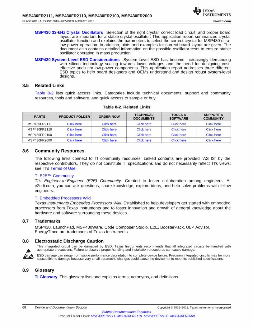
68
MSP430FR2111, MSP430FR2110, MSP430FR2100, MSP430FR2000SLASE78C –AUGUST 2016–REVISED AUGUST 2018 www.ti.com
Submit Documentation FeedbackProduct Folder Links: MSP430FR2111 MSP430FR2110 MSP430FR2100 MSP430FR2000
Device and Documentation Support Copyright © 2016–2018, Texas Instruments Incorporated
MSP430 32-kHz Crystal Oscillators Selection of the right crystal, correct load circuit, and proper boardlayout are important for a stable crystal oscillator. This application report summarizes crystaloscillator function and explains the parameters to select the correct crystal for MSP430 ultra-low-power operation. In addition, hints and examples for correct board layout are given. Thedocument also contains detailed information on the possible oscillator tests to ensure stableoscillator operation in mass production.
MSP430 System-Level ESD Considerations System-Level ESD has become increasingly demandingwith silicon technology scaling towards lower voltages and the need for designing cost-effective and ultra-low-power components. This application report addresses three differentESD topics to help board designers and OEMs understand and design robust system-leveldesigns.
8.5 Related LinksTable 8-2 lists quick access links. Categories include technical documents, support and communityresources, tools and software, and quick access to sample or buy.
Table 8-2. Related Links
PARTS PRODUCT FOLDER ORDER NOW TECHNICALDOCUMENTS
TOOLS &SOFTWARE
SUPPORT &COMMUNITY
MSP430FR2111 Click here Click here Click here Click here Click hereMSP430FR2110 Click here Click here Click here Click here Click hereMSP430FR2100 Click here Click here Click here Click here Click hereMSP430FR2000 Click here Click here Click here Click here Click here
8.6 Community ResourcesThe following links connect to TI community resources. Linked contents are provided "AS IS" by therespective contributors. They do not constitute TI specifications and do not necessarily reflect TI's views;see TI's Terms of Use.
TI E2E™ CommunityTI's Engineer-to-Engineer (E2E) Community. Created to foster collaboration among engineers. Ate2e.ti.com, you can ask questions, share knowledge, explore ideas, and help solve problems with fellowengineers.
TI Embedded Processors WikiTexas Instruments Embedded Processors Wiki. Established to help developers get started with embeddedprocessors from Texas Instruments and to foster innovation and growth of general knowledge about thehardware and software surrounding these devices.
8.7 TrademarksMSP430, LaunchPad, MSP430Ware, Code Composer Studio, E2E, BoosterPack, ULP Advisor,EnergyTrace are trademarks of Texas Instruments.
8.8 Electrostatic Discharge CautionThis integrated circuit can be damaged by ESD. Texas Instruments recommends that all integrated circuits be handled withappropriate precautions. Failure to observe proper handling and installation procedures can cause damage.
ESD damage can range from subtle performance degradation to complete device failure. Precision integrated circuits may be moresusceptible to damage because very small parametric changes could cause the device not to meet its published specifications.
8.9 GlossaryTI Glossary This glossary lists and explains terms, acronyms, and definitions.
69
MSP430FR2111, MSP430FR2110, MSP430FR2100, MSP430FR2000www.ti.com SLASE78C –AUGUST 2016–REVISED AUGUST 2018
Submit Documentation FeedbackProduct Folder Links: MSP430FR2111 MSP430FR2110 MSP430FR2100 MSP430FR2000
Mechanical, Packaging, and Orderable InformationCopyright © 2016–2018, Texas Instruments Incorporated
9 Mechanical, Packaging, and Orderable Information
The following pages include mechanical, packaging, and orderable information. This information is themost current data available for the designated devices. This data is subject to change without notice andrevision of this document. For browser-based versions of this data sheet, refer to the left-hand navigation.
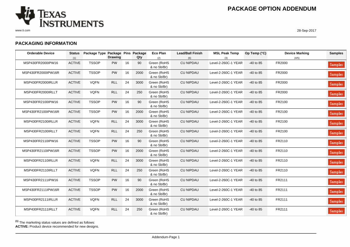
PACKAGE OPTION ADDENDUM
www.ti.com 28-Sep-2017
Addendum-Page 1
PACKAGING INFORMATION
Orderable Device Status(1)
Package Type PackageDrawing
Pins PackageQty
Eco Plan(2)
Lead/Ball Finish(6)
MSL Peak Temp(3)
Op Temp (°C) Device Marking(4/5)
Samples
MSP430FR2000IPW16 ACTIVE TSSOP PW 16 90 Green (RoHS& no Sb/Br)
CU NIPDAU Level-2-260C-1 YEAR -40 to 85 FR2000
MSP430FR2000IPW16R ACTIVE TSSOP PW 16 2000 Green (RoHS& no Sb/Br)
CU NIPDAU Level-2-260C-1 YEAR -40 to 85 FR2000
MSP430FR2000IRLLR ACTIVE VQFN RLL 24 3000 Green (RoHS& no Sb/Br)
CU NIPDAU Level-2-260C-1 YEAR -40 to 85 FR2000
MSP430FR2000IRLLT ACTIVE VQFN RLL 24 250 Green (RoHS& no Sb/Br)
CU NIPDAU Level-2-260C-1 YEAR -40 to 85 FR2000
MSP430FR2100IPW16 ACTIVE TSSOP PW 16 90 Green (RoHS& no Sb/Br)
CU NIPDAU Level-2-260C-1 YEAR -40 to 85 FR2100
MSP430FR2100IPW16R ACTIVE TSSOP PW 16 2000 Green (RoHS& no Sb/Br)
CU NIPDAU Level-2-260C-1 YEAR -40 to 85 FR2100
MSP430FR2100IRLLR ACTIVE VQFN RLL 24 3000 Green (RoHS& no Sb/Br)
CU NIPDAU Level-2-260C-1 YEAR -40 to 85 FR2100
MSP430FR2100IRLLT ACTIVE VQFN RLL 24 250 Green (RoHS& no Sb/Br)
CU NIPDAU Level-2-260C-1 YEAR -40 to 85 FR2100
MSP430FR2110IPW16 ACTIVE TSSOP PW 16 90 Green (RoHS& no Sb/Br)
CU NIPDAU Level-2-260C-1 YEAR -40 to 85 FR2110
MSP430FR2110IPW16R ACTIVE TSSOP PW 16 2000 Green (RoHS& no Sb/Br)
CU NIPDAU Level-2-260C-1 YEAR -40 to 85 FR2110
MSP430FR2110IRLLR ACTIVE VQFN RLL 24 3000 Green (RoHS& no Sb/Br)
CU NIPDAU Level-2-260C-1 YEAR -40 to 85 FR2110
MSP430FR2110IRLLT ACTIVE VQFN RLL 24 250 Green (RoHS& no Sb/Br)
CU NIPDAU Level-2-260C-1 YEAR -40 to 85 FR2110
MSP430FR2111IPW16 ACTIVE TSSOP PW 16 90 Green (RoHS& no Sb/Br)
CU NIPDAU Level-2-260C-1 YEAR -40 to 85 FR2111
MSP430FR2111IPW16R ACTIVE TSSOP PW 16 2000 Green (RoHS& no Sb/Br)
CU NIPDAU Level-2-260C-1 YEAR -40 to 85 FR2111
MSP430FR2111IRLLR ACTIVE VQFN RLL 24 3000 Green (RoHS& no Sb/Br)
CU NIPDAU Level-2-260C-1 YEAR -40 to 85 FR2111
MSP430FR2111IRLLT ACTIVE VQFN RLL 24 250 Green (RoHS& no Sb/Br)
CU NIPDAU Level-2-260C-1 YEAR -40 to 85 FR2111
(1) The marketing status values are defined as follows:ACTIVE: Product device recommended for new designs.
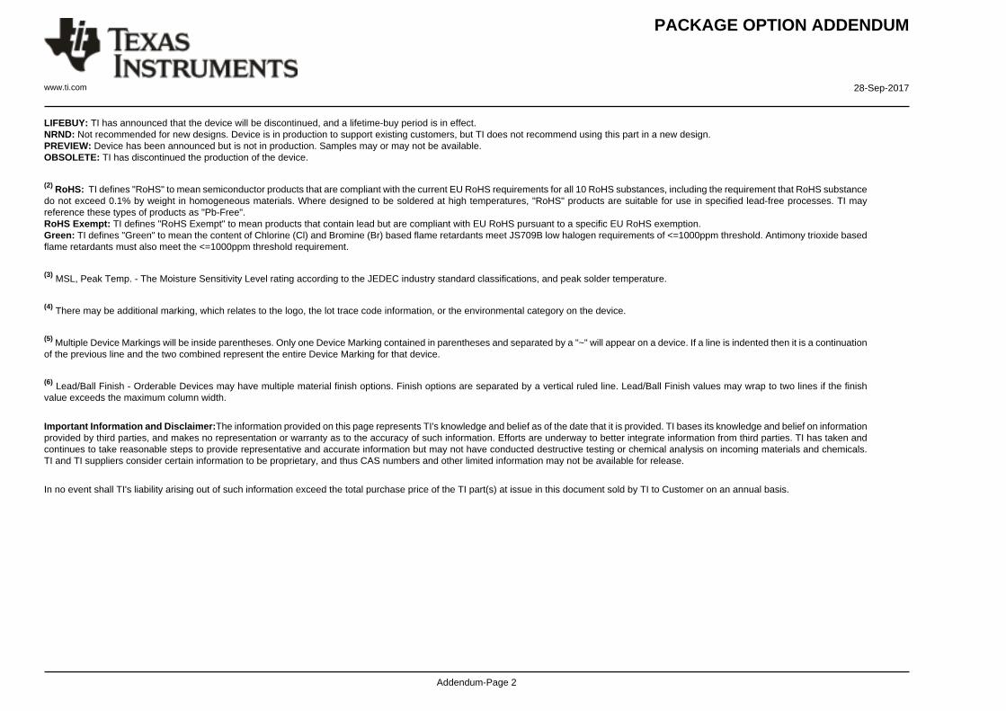
PACKAGE OPTION ADDENDUM
www.ti.com 28-Sep-2017
Addendum-Page 2
LIFEBUY: TI has announced that the device will be discontinued, and a lifetime-buy period is in effect.NRND: Not recommended for new designs. Device is in production to support existing customers, but TI does not recommend using this part in a new design.PREVIEW: Device has been announced but is not in production. Samples may or may not be available.OBSOLETE: TI has discontinued the production of the device.
(2) RoHS: TI defines "RoHS" to mean semiconductor products that are compliant with the current EU RoHS requirements for all 10 RoHS substances, including the requirement that RoHS substancedo not exceed 0.1% by weight in homogeneous materials. Where designed to be soldered at high temperatures, "RoHS" products are suitable for use in specified lead-free processes. TI mayreference these types of products as "Pb-Free".RoHS Exempt: TI defines "RoHS Exempt" to mean products that contain lead but are compliant with EU RoHS pursuant to a specific EU RoHS exemption.Green: TI defines "Green" to mean the content of Chlorine (Cl) and Bromine (Br) based flame retardants meet JS709B low halogen requirements of <=1000ppm threshold. Antimony trioxide basedflame retardants must also meet the <=1000ppm threshold requirement.
(3) MSL, Peak Temp. - The Moisture Sensitivity Level rating according to the JEDEC industry standard classifications, and peak solder temperature.
(4) There may be additional marking, which relates to the logo, the lot trace code information, or the environmental category on the device.
(5) Multiple Device Markings will be inside parentheses. Only one Device Marking contained in parentheses and separated by a "~" will appear on a device. If a line is indented then it is a continuationof the previous line and the two combined represent the entire Device Marking for that device.
(6) Lead/Ball Finish - Orderable Devices may have multiple material finish options. Finish options are separated by a vertical ruled line. Lead/Ball Finish values may wrap to two lines if the finishvalue exceeds the maximum column width.
Important Information and Disclaimer:The information provided on this page represents TI's knowledge and belief as of the date that it is provided. TI bases its knowledge and belief on informationprovided by third parties, and makes no representation or warranty as to the accuracy of such information. Efforts are underway to better integrate information from third parties. TI has taken andcontinues to take reasonable steps to provide representative and accurate information but may not have conducted destructive testing or chemical analysis on incoming materials and chemicals.TI and TI suppliers consider certain information to be proprietary, and thus CAS numbers and other limited information may not be available for release.
In no event shall TI's liability arising out of such information exceed the total purchase price of the TI part(s) at issue in this document sold by TI to Customer on an annual basis.
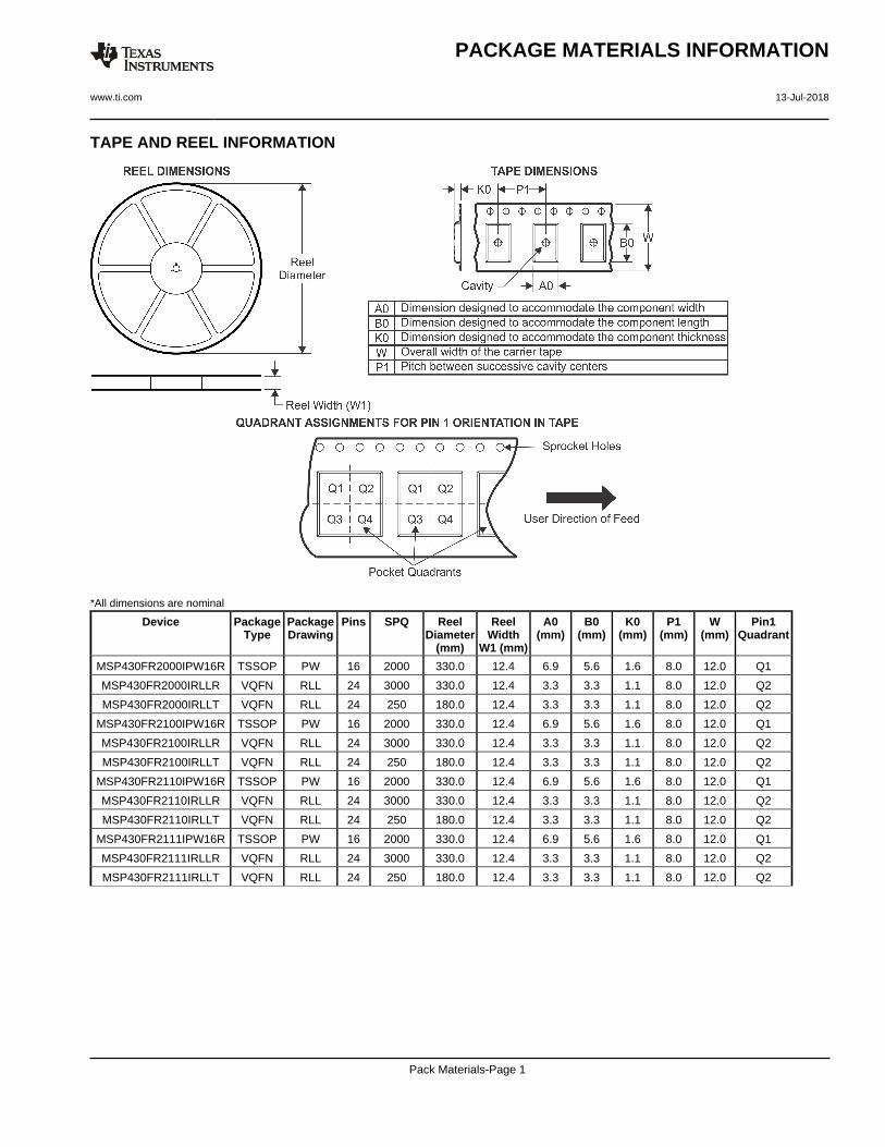
TAPE AND REEL INFORMATION
*All dimensions are nominal
Device PackageType
PackageDrawing
Pins SPQ ReelDiameter
(mm)
ReelWidth
W1 (mm)
A0(mm)
B0(mm)
K0(mm)
P1(mm)
W(mm)
Pin1Quadrant
MSP430FR2000IPW16R TSSOP PW 16 2000 330.0 12.4 6.9 5.6 1.6 8.0 12.0 Q1
MSP430FR2000IRLLR VQFN RLL 24 3000 330.0 12.4 3.3 3.3 1.1 8.0 12.0 Q2
MSP430FR2000IRLLT VQFN RLL 24 250 180.0 12.4 3.3 3.3 1.1 8.0 12.0 Q2
MSP430FR2100IPW16R TSSOP PW 16 2000 330.0 12.4 6.9 5.6 1.6 8.0 12.0 Q1
MSP430FR2100IRLLR VQFN RLL 24 3000 330.0 12.4 3.3 3.3 1.1 8.0 12.0 Q2
MSP430FR2100IRLLT VQFN RLL 24 250 180.0 12.4 3.3 3.3 1.1 8.0 12.0 Q2
MSP430FR2110IPW16R TSSOP PW 16 2000 330.0 12.4 6.9 5.6 1.6 8.0 12.0 Q1
MSP430FR2110IRLLR VQFN RLL 24 3000 330.0 12.4 3.3 3.3 1.1 8.0 12.0 Q2
MSP430FR2110IRLLT VQFN RLL 24 250 180.0 12.4 3.3 3.3 1.1 8.0 12.0 Q2
MSP430FR2111IPW16R TSSOP PW 16 2000 330.0 12.4 6.9 5.6 1.6 8.0 12.0 Q1
MSP430FR2111IRLLR VQFN RLL 24 3000 330.0 12.4 3.3 3.3 1.1 8.0 12.0 Q2
MSP430FR2111IRLLT VQFN RLL 24 250 180.0 12.4 3.3 3.3 1.1 8.0 12.0 Q2
PACKAGE MATERIALS INFORMATION
www.ti.com 13-Jul-2018
Pack Materials-Page 1

*All dimensions are nominal
Device Package Type Package Drawing Pins SPQ Length (mm) Width (mm) Height (mm)
MSP430FR2000IPW16R TSSOP PW 16 2000 367.0 367.0 38.0
MSP430FR2000IRLLR VQFN RLL 24 3000 367.0 367.0 35.0
MSP430FR2000IRLLT VQFN RLL 24 250 210.0 185.0 35.0
MSP430FR2100IPW16R TSSOP PW 16 2000 367.0 367.0 38.0
MSP430FR2100IRLLR VQFN RLL 24 3000 367.0 367.0 35.0
MSP430FR2100IRLLT VQFN RLL 24 250 210.0 185.0 35.0
MSP430FR2110IPW16R TSSOP PW 16 2000 367.0 367.0 38.0
MSP430FR2110IRLLR VQFN RLL 24 3000 367.0 367.0 35.0
MSP430FR2110IRLLT VQFN RLL 24 250 210.0 185.0 35.0
MSP430FR2111IPW16R TSSOP PW 16 2000 350.0 350.0 43.0
MSP430FR2111IRLLR VQFN RLL 24 3000 367.0 367.0 35.0
MSP430FR2111IRLLT VQFN RLL 24 250 210.0 185.0 35.0
PACKAGE MATERIALS INFORMATION
www.ti.com 13-Jul-2018
Pack Materials-Page 2
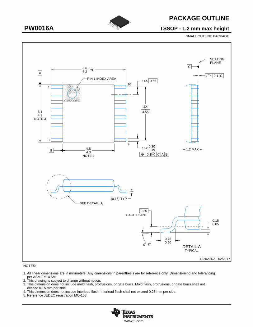
www.ti.com
PACKAGE OUTLINE
C
14X 0.65
2X4.55
16X 0.300.19
TYP6.66.2
1.2 MAX
0.150.05
0.25GAGE PLANE
-80
BNOTE 4
4.54.3
A
NOTE 3
5.14.9
0.750.50
(0.15) TYP
TSSOP - 1.2 mm max heightPW0016ASMALL OUTLINE PACKAGE
4220204/A 02/2017
1
89
16
0.1 C A B
PIN 1 INDEX AREA
SEE DETAIL A
0.1 C
NOTES: 1. All linear dimensions are in millimeters. Any dimensions in parenthesis are for reference only. Dimensioning and tolerancing per ASME Y14.5M. 2. This drawing is subject to change without notice. 3. This dimension does not include mold flash, protrusions, or gate burrs. Mold flash, protrusions, or gate burrs shall not exceed 0.15 mm per side. 4. This dimension does not include interlead flash. Interlead flash shall not exceed 0.25 mm per side.5. Reference JEDEC registration MO-153.
SEATINGPLANE
A 20DETAIL ATYPICAL
SCALE 2.500
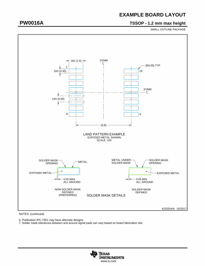
www.ti.com
EXAMPLE BOARD LAYOUT
0.05 MAXALL AROUND
0.05 MINALL AROUND
16X (1.5)
16X (0.45)
14X (0.65)
(5.8)
(R0.05) TYP
TSSOP - 1.2 mm max heightPW0016ASMALL OUTLINE PACKAGE
4220204/A 02/2017
NOTES: (continued) 6. Publication IPC-7351 may have alternate designs. 7. Solder mask tolerances between and around signal pads can vary based on board fabrication site.
LAND PATTERN EXAMPLEEXPOSED METAL SHOWN
SCALE: 10X
SYMM
SYMM
1
8 9
16
15.000
METALSOLDER MASKOPENING
METAL UNDERSOLDER MASK
SOLDER MASKOPENING
EXPOSED METALEXPOSED METAL
SOLDER MASK DETAILS
NON-SOLDER MASKDEFINED
(PREFERRED)
SOLDER MASKDEFINED
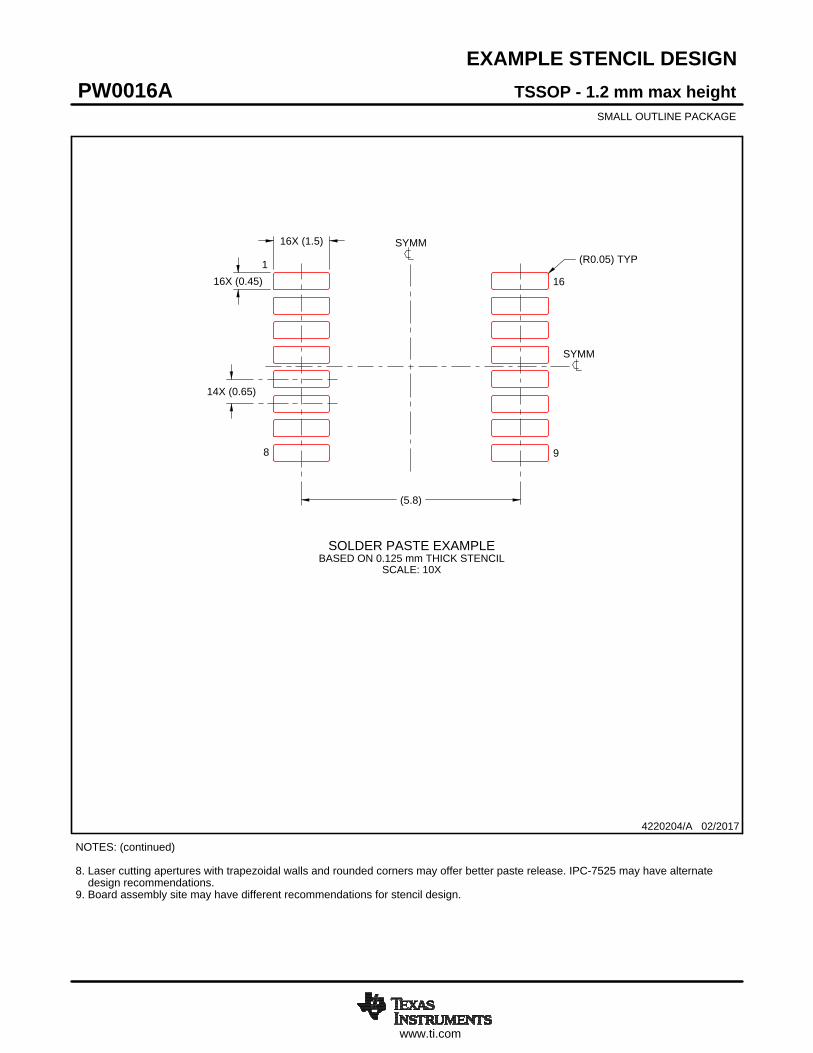
www.ti.com
EXAMPLE STENCIL DESIGN
16X (1.5)
16X (0.45)
14X (0.65)
(5.8)
(R0.05) TYP
TSSOP - 1.2 mm max heightPW0016ASMALL OUTLINE PACKAGE
4220204/A 02/2017
NOTES: (continued) 8. Laser cutting apertures with trapezoidal walls and rounded corners may offer better paste release. IPC-7525 may have alternate design recommendations. 9. Board assembly site may have different recommendations for stencil design.
SOLDER PASTE EXAMPLEBASED ON 0.125 mm THICK STENCIL
SCALE: 10X
SYMM
SYMM
1
8 9
16
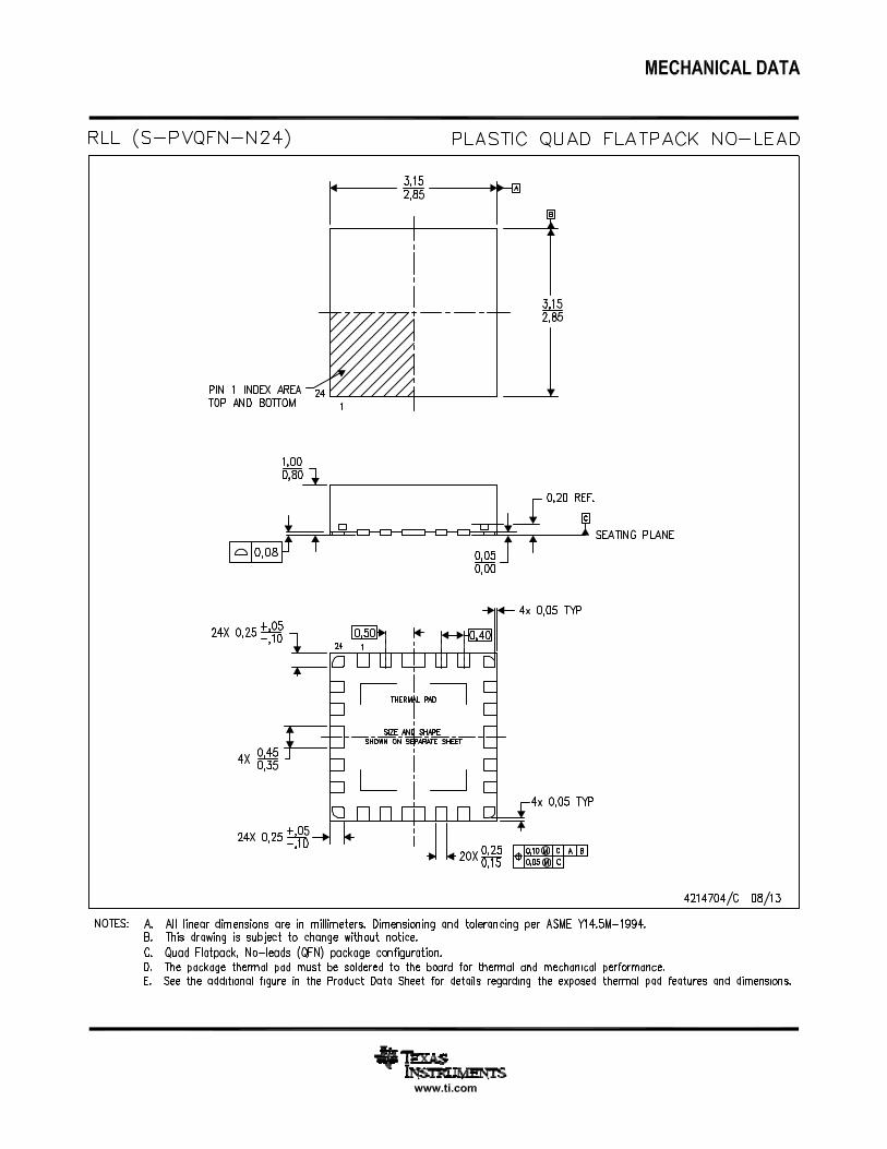
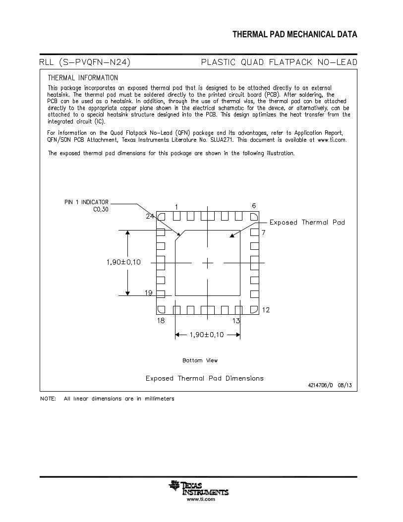

IMPORTANT NOTICE AND DISCLAIMER
TI PROVIDES TECHNICAL AND RELIABILITY DATA (INCLUDING DATASHEETS), DESIGN RESOURCES (INCLUDING REFERENCEDESIGNS), APPLICATION OR OTHER DESIGN ADVICE, WEB TOOLS, SAFETY INFORMATION, AND OTHER RESOURCES “AS IS”AND WITH ALL FAULTS, AND DISCLAIMS ALL WARRANTIES, EXPRESS AND IMPLIED, INCLUDING WITHOUT LIMITATION ANYIMPLIED WARRANTIES OF MERCHANTABILITY, FITNESS FOR A PARTICULAR PURPOSE OR NON-INFRINGEMENT OF THIRDPARTY INTELLECTUAL PROPERTY RIGHTS.These resources are intended for skilled developers designing with TI products. You are solely responsible for (1) selecting the appropriateTI products for your application, (2) designing, validating and testing your application, and (3) ensuring your application meets applicablestandards, and any other safety, security, or other requirements. These resources are subject to change without notice. TI grants youpermission to use these resources only for development of an application that uses the TI products described in the resource. Otherreproduction and display of these resources is prohibited. No license is granted to any other TI intellectual property right or to any thirdparty intellectual property right. TI disclaims responsibility for, and you will fully indemnify TI and its representatives against, any claims,damages, costs, losses, and liabilities arising out of your use of these resources.TI’s products are provided subject to TI’s Terms of Sale (www.ti.com/legal/termsofsale.html) or other applicable terms available either onti.com or provided in conjunction with such TI products. TI’s provision of these resources does not expand or otherwise alter TI’s applicablewarranties or warranty disclaimers for TI products.
Mailing Address: Texas Instruments, Post Office Box 655303, Dallas, Texas 75265Copyright © 2018, Texas Instruments Incorporated