Embed Size (px)
Citation preview
MSP430 Keeping Time
© 2013 Stephen R. Platt ME 461 1
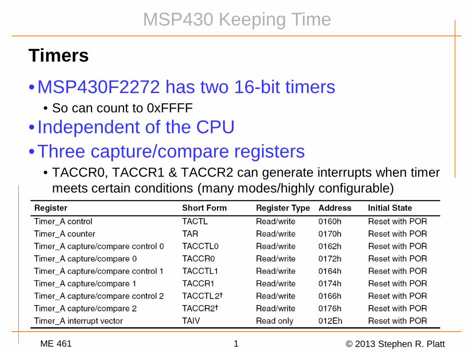
Timers •MSP430F2272 has two 16-bit timers
• So can count to 0xFFFF • Independent of the CPU •Three capture/compare registers
• TACCR0, TACCR1 & TACCR2 can generate interrupts when timer meets certain conditions (many modes/highly configurable)
MSP430 Keeping Time
© 2013 Stephen R. Platt ME 461 2
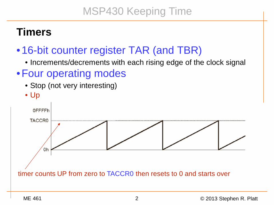
Timers •16-bit counter register TAR (and TBR)
• Increments/decrements with each rising edge of the clock signal •Four operating modes
• Stop (not very interesting)
timer counts UP from zero to TACCR0 then resets to 0 and starts over
• Up
MSP430 Timers & Interrupts
© 2013 Stephen R. Platt ME 461 3
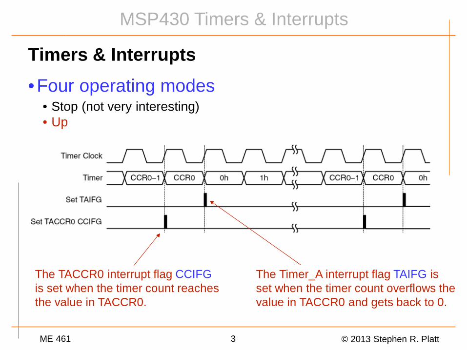
Timers & Interrupts •Four operating modes
• Stop (not very interesting) • Up
The TACCR0 interrupt flag CCIFG is set when the timer count reaches the value in TACCR0.
The Timer_A interrupt flag TAIFG is set when the timer count overflows the value in TACCR0 and gets back to 0.
MSP430 Timers & Interrupts
© 2013 Stephen R. Platt ME 461 4
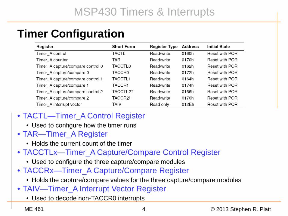
Timer Configuration
• TACTL—Timer_A Control Register • Used to configure how the timer runs
• TAR—Timer_A Register • Holds the current count of the timer
• TACCTLx—Timer_A Capture/Compare Control Register • Used to configure the three capture/compare modules
• TACCRx—Timer_A Capture/Compare Register • Holds the capture/compare values for the three capture/compare modules
• TAIV—Timer_A Interrupt Vector Register • Used to decode non-TACCR0 interrupts
MSP430 Timers & Interrupts
© 2013 Stephen R. Platt ME 461 5
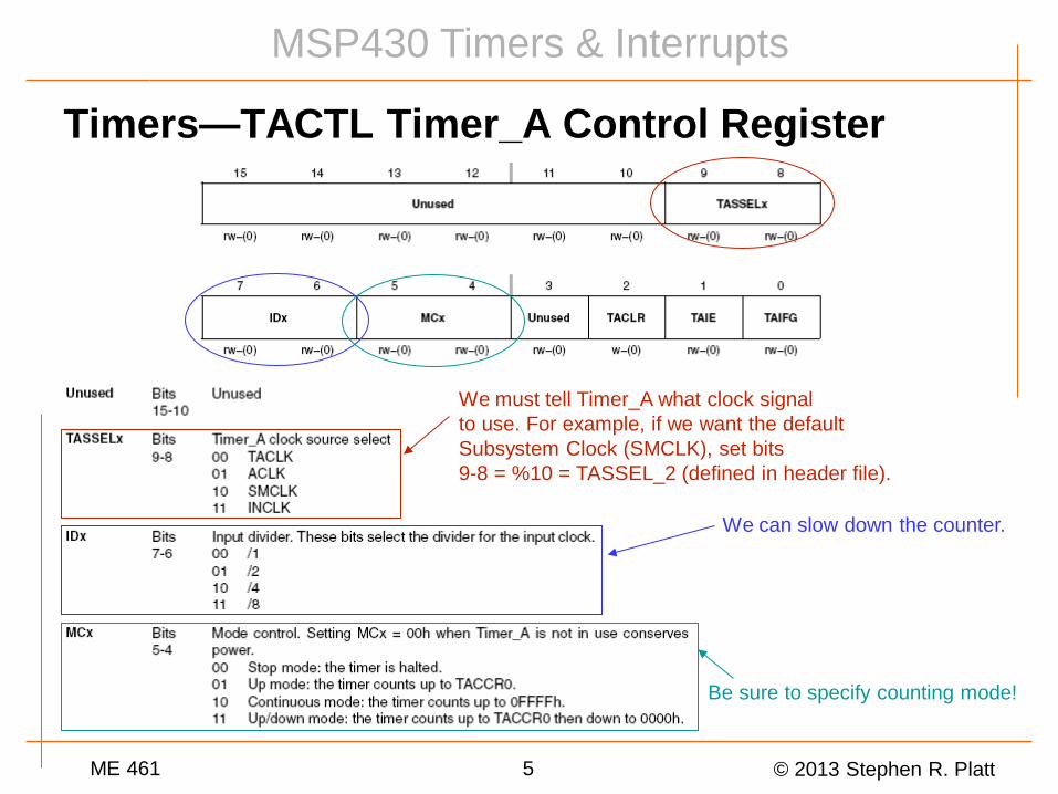
Timers—TACTL Timer_A Control Register
We must tell Timer_A what clock signal to use. For example, if we want the default Subsystem Clock (SMCLK), set bits 9-8 = %10 = TASSEL_2 (defined in header file).
We can slow down the counter.
Be sure to specify counting mode!
Timer_A Registers www.ti.com
12.3.1 TACTL, Timer_A Control Register
15 14 13 12 11 10 9 8
Unused TASSELx
rw-(0) rw-(0) rw-(0) rw-(0) rw-(0) rw-(0) rw-(0) rw-(0)
7 6 5 4 3 2 1 0
IDx MCx Unused TACLR TAIE TAIFG
rw-(0) rw-(0) rw-(0) rw-(0) rw-(0) rw-(0) rw-(0) rw-(0)
Unused Bits 15-10 Unused
TASSELx Bits 9-8 Timer_A clock source select
00 TACLK
01 ACLK
10 SMCLK
11 INCLK (INCLK is device-specific and is often assigned to the inverted TBCLK) (see thedevice-specific data sheet)
IDx Bits 7-6 Input divider. These bits select the divider for the input clock.
00 /1
01 /2
10 /4
11 /8
MCx Bits 5-4 Mode control. Setting MCx = 00h when Timer_A is not in use conserves power.
00 Stop mode: the timer is halted.
01 Up mode: the timer counts up to TACCR0.
10 Continuous mode: the timer counts up to 0FFFFh.
11 Up/down mode: the timer counts up to TACCR0 then down to 0000h.
Unused Bit 3 Unused
TACLR Bit 2 Timer_A clear. Setting this bit resets TAR, the clock divider, and the count direction. The TACLR bit isautomatically reset and is always read as zero.
TAIE Bit 1 Timer_A interrupt enable. This bit enables the TAIFG interrupt request.
0 Interrupt disabled
1 Interrupt enabled
TAIFG Bit 0 Timer_A interrupt flag
0 No interrupt pending
1 Interrupt pending
378 Timer_A SLAU144I–December 2004–Revised January 2012Submit Documentation Feedback
Copyright © 2004–2012, Texas Instruments Incorporated
MSP430 Timers & Interrupts
© 2013 Stephen R. Platt ME 461 6
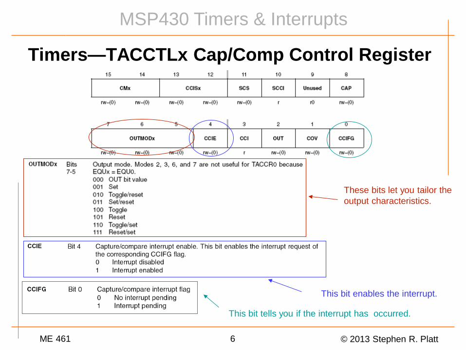
Timers—TACCTLx Cap/Comp Control Register
These bits let you tailor the output characteristics.
This bit enables the interrupt.
This bit tells you if the interrupt has occurred.

Timer_A Registers www.ti.com
12.3.4 TACCTLx, Capture/Compare Control Register
15 14 13 12 11 10 9 8
CMx CCISx SCS SCCI Unused CAP
rw-(0) rw-(0) rw-(0) rw-(0) rw-(0) r r0 rw-(0)
7 6 5 4 3 2 1 0
OUTMODx CCIE CCI OUT COV CCIFG
rw-(0) rw-(0) rw-(0) rw-(0) r rw-(0) rw-(0) rw-(0)
CMx Bit 15-14 Capture mode
00 No capture
01 Capture on rising edge
10 Capture on falling edge
11 Capture on both rising and falling edges
CCISx Bit 13-12 Capture/compare input select. These bits select the TACCRx input signal. See the device-specific datasheet for specific signal connections.
00 CCIxA
01 CCIxB
10 GND
11 VCC
SCS Bit 11 Synchronize capture source. This bit is used to synchronize the capture input signal with the timer clock.
0 Asynchronous capture
1 Synchronous capture
SCCI Bit 10 Synchronized capture/compare input. The selected CCI input signal is latched with the EQUx signal and canbe read via this bit
Unused Bit 9 Unused. Read only. Always read as 0.
CAP Bit 8 Capture mode
0 Compare mode
1 Capture mode
OUTMODx Bits 7-5 Output mode. Modes 2, 3, 6, and 7 are not useful for TACCR0, because EQUx = EQU0.
000 OUT bit value
001 Set
010 Toggle/reset
011 Set/reset
100 Toggle
101 Reset
110 Toggle/set
111 Reset/set
CCIE Bit 4 Capture/compare interrupt enable. This bit enables the interrupt request of the corresponding CCIFG flag.
0 Interrupt disabled
1 Interrupt enabled
CCI Bit 3 Capture/compare input. The selected input signal can be read by this bit.
OUT Bit 2 Output. For output mode 0, this bit directly controls the state of the output.
0 Output low
1 Output high
COV Bit 1 Capture overflow. This bit indicates a capture overflow occurred. COV must be reset with software.
0 No capture overflow occurred
1 Capture overflow occurred
CCIFG Bit 0 Capture/compare interrupt flag
0 No interrupt pending
1 Interrupt pending
380 Timer_A SLAU144I–December 2004–Revised January 2012Submit Documentation Feedback
Copyright © 2004–2012, Texas Instruments Incorporated
MSP430 Timers & Interrupts
© 2013 Stephen R. Platt ME 461 7
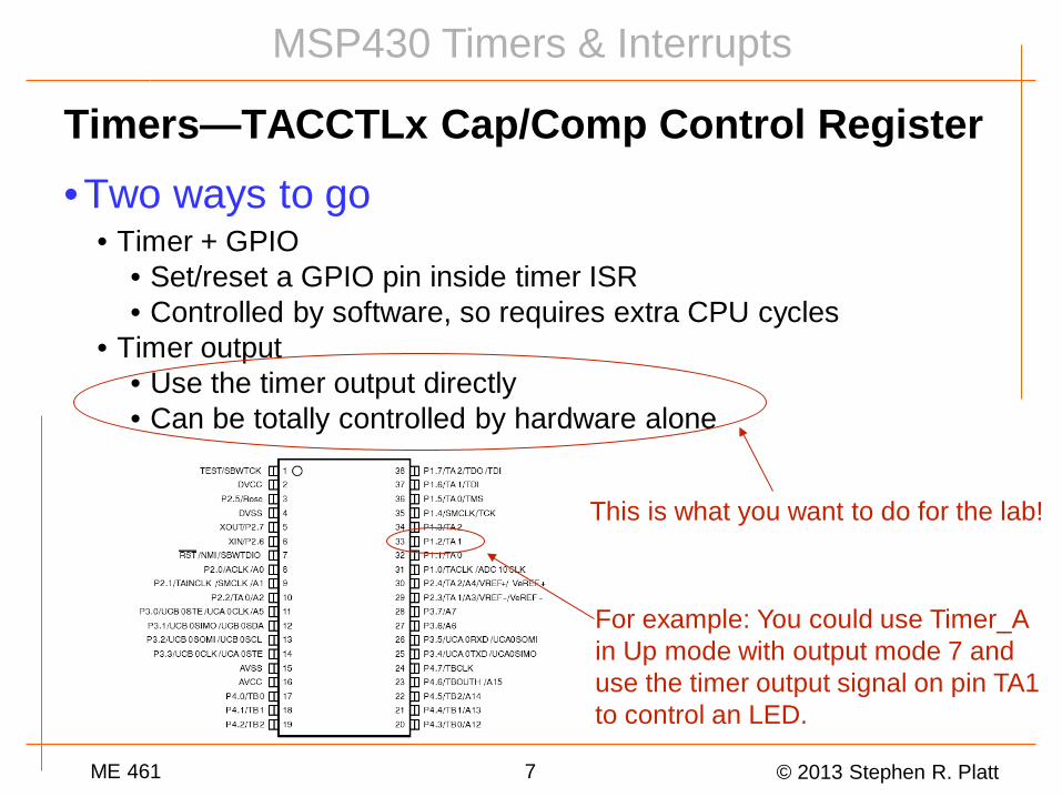
Timers—TACCTLx Cap/Comp Control Register •Two ways to go
• Timer + GPIO • Set/reset a GPIO pin inside timer ISR • Controlled by software, so requires extra CPU cycles
• Timer output • Use the timer output directly • Can be totally controlled by hardware alone
This is what you want to do for the lab!
For example: You could use Timer_A in Up mode with output mode 7 and use the timer output signal on pin TA1 to control an LED.
MSP430 Timers & Interrupts
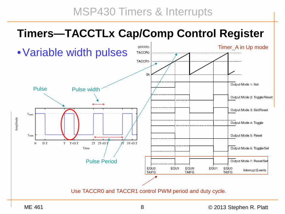
© 2013 Stephen R. Platt ME 461 8
Timers—TACCTLx Cap/Comp Control Register •Variable width pulses
Pulse Period
Use TACCR0 and TACCR1 control PWM period and duty cycle.
Pulse Pulse width
Timer_A in Up mode
MSP430 PWM & DAC
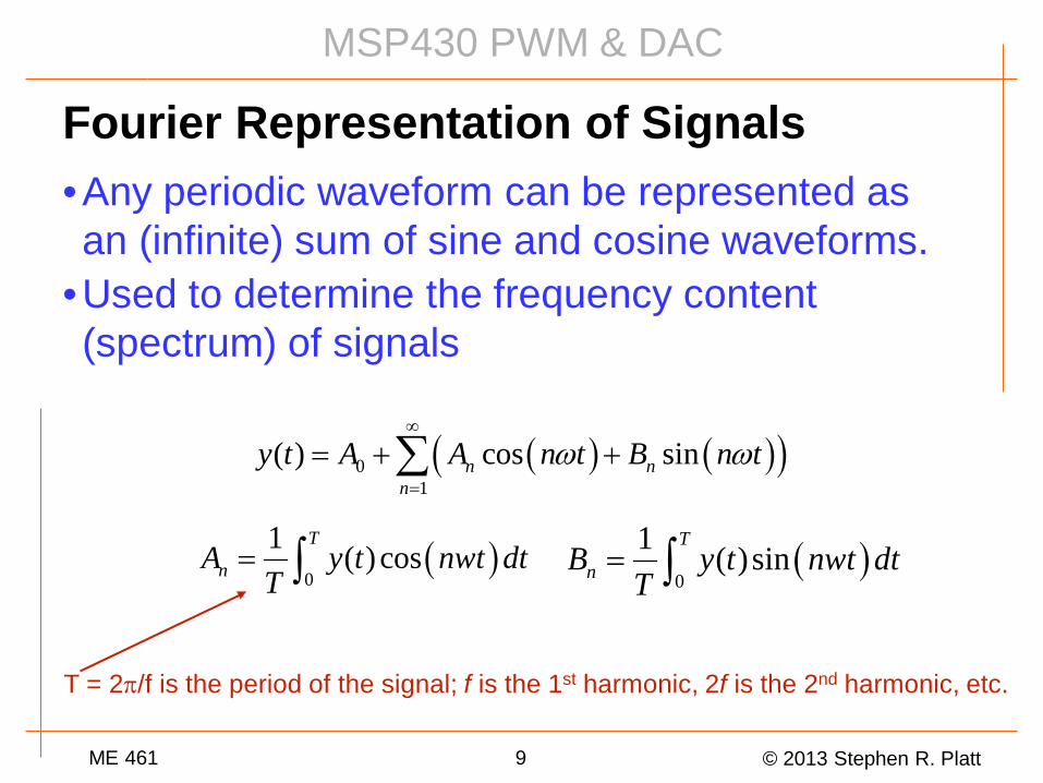
© 2013 Stephen R. Platt ME 461 9
Fourier Representation of Signals •Any periodic waveform can be represented as an (infinite) sum of sine and cosine waveforms.
•Used to determine the frequency content (spectrum) of signals
T = 2π/f is the period of the signal; f is the 1st harmonic, 2f is the 2nd harmonic, etc.
( ) ( )( )01
( ) cos sinω ω∞
=
= + +∑ n nn
y t A A n t B n t
( )0
1 ( ) cos= ∫T
nA y t nwt dtT ( )
0
1 ( )sin= ∫T
nB y t nwt dtT
MSP430 PWM & DAC
© 2013 Stephen R. Platt ME 461 10
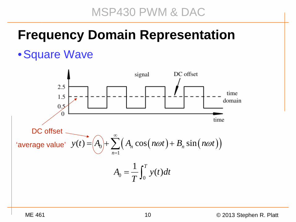
Frequency Domain Representation •Square Wave
( ) ( )( )01
( ) cos sinω ω∞
=
= + +∑ n nn
y t A A n t B n tDC offset
0 0
1 ( )= ∫T
A y t dtT
‘average value’
MSP430 PWM & DAC
© 2013 Stephen R. Platt ME 461 11
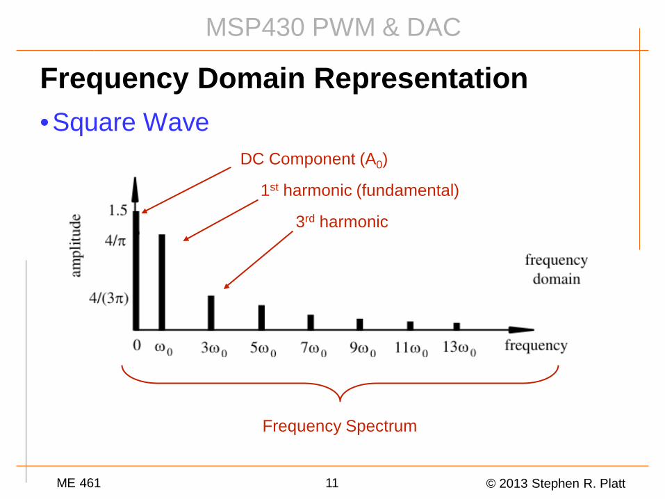
Frequency Domain Representation •Square Wave
DC Component (A0)
1st harmonic (fundamental)
3rd harmonic
Frequency Spectrum
MSP430 PWM & DAC
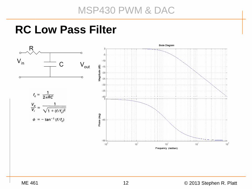
© 2013 Stephen R. Platt ME 461 12
RC Low Pass Filter