Embed Size (px)
Citation preview

i
Version 6.0G52-MA00522
MS-6368 (v6.X) Micro-ATX Mainboard
MSIMICRO-STAR INTERNATIONAL

ii
Manual Rev: 6.0Release Date: Feb. 2002
FCC-B Radio Frequency Interference Statement
This equipment has been tested and found to comply with the limits for a classB digital device, pursuant to part 15 of the FCC rules. These limits are designedto provide reasonable protection against harmful interference when the equip-ment is operated in a commercial environment. This equipment generates, usesand can radiate radio frequency energy and, if not installed and used in accor-dance with the instruction manual, may cause harmful interference to radiocommunications. Operation of this equipment in a residential area is likely tocause harmful interference, in which case the user will be required to correctthe interference at his own expense.
Notice 1The changes or modifications not expressly approved by the party respon-sible for compliance could void the user’s authority to operate the equipment.
Notice 2Shielded interface cables and A.C. power cord, if any, must be used in order tocomply with the emission limits.
VOIR LA NOTICE D’INSTALLATION AVANT DE RACCORDER AURESEAU.
Micro-Star International MS-6368
Tested to comply with FCC Standard
For Home or Office Use

iii
EditionFeb. 2002
Copyright Notice
The material in this document is the intellectual property of MICRO-STAR INTERNATIONAL. We take every care in the preparationof this document, but no guarantee is given as to the correctness of itscontents. Our products are under continual improvement and we re-serve the right to make changes without notice.
TrademarksAll trademarks used in this manual are the property of their respectiveowners.
Intel and Pentium are registered trademarks of Intel Corporation.PS/2 and OS/2 are registered trademarks of IBM Corporation.Windows 98/2000/ME and Windows NT are registered trademarks ofMicrosoft.Netware is a registered trademark of Novell.Award is a registered trademark of Award Software Inc.
Revision HistoryRevision Revision History Date6.0 First release for PCB 6.X Feb. 2001

iv
1. Always read the safety instructions carefully.2. Keep this User’s Manual for future reference.3. Keep this equipment away from humidity.4. Lay this equipment on a reliable flat surface before setting it up.5. The openings on the enclosure are for air convection hence protects the
equipment from overheating. DO NOT COVER THE OPENINGS.6. Make sure the voltage of the power source and adjust properly 110/220V
before connecting the equipment to the power inlet.7. Place the power cord such a way that people can not step on it. Do not
place anything over the power cord.8. Always Unplug the Power Cord before inserting any add-on card or module.9. All cautions and warnings on the equipment should be noted.10. Never pour any liquid into the opening that could damage or cause electri-
cal shock.11. If any of the following situations arises, get the equipment checked by a
service personnel:The power cord or plug is damagedLiquid has penetrated into the equipmentThe equipment has been exposed to moistureThe equipment has not work well or you can not get it work accordingto User’s Manual.The equipment has dropped and damagedIf the equipment has obvious sign of breakage
12. DO NOT LEAVE THIS EQUIPMENT IN AN ENVIRONMENTUNCONDITIONED, STORAGE TEMPERATURE ABOVE 600 C (1400F), ITMAY DAMAGE THE EQUIPMENT.
Safety Instructions
CAUTION: Danger of explosion if battery is incorrectly replaced.Replace only with the same or equivalent type recommended by themanufacturer.

v
ContentsChapter 1. Introduction ............................................................................ 1-1
Mainboard Specification ...................................................................... 1-2Mainboard Layout ............................................................................... 1-4Quick Components Guide .................................................................... 1-5
Chapter 2. Hardware Setup ...................................................................... 2-1Central Processing Unit: CPU .............................................................. 2-2
CPU Installation Procedures ......................................................... 2-2CPU Core Speed Derivation Procedure ......................................... 2-3
Memory ................................................................................................ 2-4Introduction to SDRAM ............................................................... 2-4Installing DIMM Modules ............................................................ 2-4DIMM Modules Combination ....................................................... 2-5
Power Supply ....................................................................................... 2-6ATX 20-Pin Power Supply ............................................................. 2-6
Back Panel ............................................................................................ 2-7Mouse Connector ......................................................................... 2-7Keyboard Connector ..................................................................... 2-8USB Connectors ............................................................................ 2-8Parallel Port Connector .................................................................. 2-9Serial Port Connector: COM 1 & COM 2 ..................................... 2-10VGA DB 15 Pin Connector .......................................................... 2-10LAN Jack (RJ-45) (Optional) ........................................................ 2-11Joystick/Midi Connectors ........................................................... 2-11Audio Port Connectors ............................................................... 2-11
Connectors ......................................................................................... 2-12Floppy Disk Drive Connector: FDD1........................................... 2-12CD-In Connector: JCD1 ............................................................... 2-12Hard Disk Connectors: IDE1 & IDE2 ........................................... 2-13Front Panel Connector: JFP1/JFP2 .............................................. 2-14

vi
Wake On Ring Connector: JWR1 ................................................ 2-15Wake On LAN Connector: JWOL1 .............................................. 2-15Fan Power Connectors: CFAN1/SFAN1 ...................................... 2-16IrDA Infrared Module Connector: JIR1 ....................................... 2-17Front USB Connectors: JUSB1 .................................................... 2-17Front Panel Audio Connector: JAUD1 ........................................ 2-18
Jumpers .............................................................................................. 2-19Clear CMOS Jumper: JBAT1 ........................................................ 2-19BIOS Flash Jumper: JBIOS1 ......................................................... 2-20
Slots ................................................................................................... 2-21PCI Slots ...................................................................................... 2-21CNR (Communication Network Riser) Slot .................................. 2-21ISA Slot (Optional) ...................................................................... 2-21PCI Interrupt Request Routing .................................................... 2-22
Chapter 3. AWARD® BIOS Setup ........................................................... 3-1Entering Setup ...................................................................................... 3-2Control Keys ........................................................................................ 3-2Getting Help ......................................................................................... 3-3The Main Menu ................................................................................... 3-4Standard CMOS Features .................................................................... 3-6Advanced BIOS Features .................................................................... 3-9Advanced Chipset Features ............................................................... 3-13Integrated Peripherals ........................................................................ 3-17Power Management Setup ................................................................. 3-22PnP/PCI Configurations ..................................................................... 3-28PC Health Status ................................................................................ 3-30Frequency/Voltage Control ................................................................ 3-31Load Fail-Safe/Optimized Defaults ..................................................... 3-32Set Supervisor/User Password ........................................................... 3-34Save & Exit Setup ............................................................................... 3-36

vii
Exit Without Saving ........................................................................... 3-37Glossary ....................................................................................................G-1

Introduction
1-1
Chapter 1 .Introduction
Thank you for purchasing the MS-6368 (v6.X) Micro-ATXmotherboard. The mainboard, based on VIA® Apollo PLE133T (VT8601T& VT82C686B) chipsets, is a high-performance computer mainboarddesigned for Intel® Celeron® /Coppermine®/Tualatin and VIA C3™ proces-sors in the 370 pin package that provides a cost-effective and professionalvalue PC platform solution.
This chapter includes the following topics:
Mainboard Specification 1-2Mainboard Layout 1-4Quick Components Guide 1-5Key Features 1-6
1

Chapter 1
1-2
CPUSocket 370 for Intel® Celeron®/Coppermine®/Tualatin processors and VIAC3™ processorSupports 500MHZ, 533MHz., 550MHz, 667MHz, 700Mhz, 750MHz,800MHz, 850MHz, 933MHz, 950MHz, 1GHz, 1.13GHz, 1.2GHz and above
ChipsetVIA® PLE133T VT8601T chipset (552 BGA)- FSB @133MHz- Integrated Trident Blade 2D/3D video accelerator- PCI Advanced high performance memory controller- Supports PC100/133 SDRAM, VCM & ESDRAM technologyVIA® VT686B chipset (352 BGA)- Enhanced Power Management Features- Integrated Super I/O (FDC, LPT, COM 1/2, and IR)- Dual bus Master IDE Ultra DMA33/66/100- Integrated Hardware Soundblaster- Direct Sound AC97 Audio- ACPI
Clock Generator66.6MHz, 100MHz and 133MHz clocks are supported
Main MemorySupports four memory banks using two 168-pin unbuffered DIMMSupports a maximum memory size of 1GB (32M x 8)Supports 3.3v SDRAM DIMM
Slots One CNR (Communication Network Riser) slot Three 32-bit Master PCI Bus slotsSupports 3.3v/5v PCI bus InterfaceOne ISA slot (optional)
On-Board IDEAn IDE controller on the VIA® VT82C686B chipset provides IDE HDD/
Mainboard Specification

Introduction
1-3
CD-ROM with PIO, Bus Master and Ultra DMA 33/66/100 operationmodes.Can connect up to four IDE devices
AudioAudio controller integrated in 686B chipsetSW Audio Codec Realtek ALC 101T- Front Audio Pin Header onboard
NetworkAdmtek 983B
On-Board PeripheralsOn-Board Peripherals include:
- 1 floppy port supports 2 FDDs with 360K, 720K, 1.2M,1.44M and 2.88Mbytes.
- 2 serial ports (COMA + COMB)- 1 parallel port supports SPP/EPP/ECP mode- 4 USB ports (2 Rear Connectors/USB Front Pin Header)- 1 IrDA connector for SIR/CIR/FIR/ASKIR/HPSIR- 1 VGA connector- 1 Audio/Game port
BIOSThe mainboard BIOS provides “Plug & Play” BIOS which detects theperipheral devices and expansion cards of the board automatically.The mainboard provides a Desktop Management Interface (DMI) func-tion which records your mainboard specifications.
DimensionMicro-ATX Form Factor: 24.5cm (L) x 21cm (W)
Mounting6 mounting holes

Chapter 1
1-4
Mainboard Layout
MS-6368 (v6.X) Micro-ATX Mainboard
BATT+
VT82C686B
VT8601T
JAUD1
JIR1JUSB1
ATX
Po
wer
Sup
ply
JFP2
JFP1
CFAN1
SFAN1
BIOS
PCI Slot 1
PCI Slot 2
PCI Slot 3
IDE
1
IDE
2DIM
M 2
DIM
M 1
CNR
ISA Slot(optional)
Top : Parallel Port
Bottom: COM Port &VGA Port
Top : mouse Bottom : keyboard
JCD
1
ADMtekAN983B
(optional)
Top :Game Port
Bottom: Line-OutLine-InMic
SOC
KE
T 37
0
FDD
1
COM 2
JWR1 JWOL1 JBIOS1

Introduction
1-5
Quick Components Guide
Component Function Reference
Socket 370 Installing CPU See p. 2-2~2-3
DIMM1 & DIMM2 Installing DIMM modules See p. 2-4~2-5
ATX Power Supply Connecting to ATX Power Supply See p. 2-6
FDD1 Connecting to FDD See p. 2-12
JCD1 Connecting to CD-ROM audio device See p. 2-12
IDE1 & IDE2 Connecting to HDD See p.2-13
JFP1& JFP2 Connecting to front panel switches/LED See p.2-14
JWR1 Connecting to modem card See p. 2-15
JWOL1 Connecting to LAN card See p. 2-15
CFAN1 Connecting to processor fan See p. 2-16
SFAN1 Connecting to system fan See p. 2-16
JIR1 Connecting to IR module See p. 2-17
JUSB1 Connecting to Front USB device See p. 2-17
JAUD1 Connecting to front panel audio See p. 2-18
JBAT1 Setting clear CMOS See p. 2-19
JBIOS1 Setting BIOS flash function See p. 2-20
PCI Slots Installing PCI card See p. 2-21
CNR Slot Installing CNR card See p. 2-21
ISA Slot Installing ISA card See p. 2-21

Hardware Setup
2-1
Hardware SetupThis chapter provides you with the information about hardware setup
procedures. While doing the installation, be careful in holding the compo-nents and follow the installation procedures. For some components, if youinstall in the wrong orientation, the components will not work properly.
Use a grounded wrist strap before handling computer components.Static electricity may damage the components.
This chapter contains the following topics:
Central Processing Unit (CPU) 2-2Memory 2-4Power Supply 2-6Back Panel 2-7Connectors 2-12Jumpers 2-19Slots 2-22
2Chapter 2. Hardware Setup

Chapter 2
2-2
The mainboard supports Intel® Celeron®/Coppermine®/Tualatin andVIA C3™ processors. The mainboard uses a CPU socket called Socket 370for easy CPU installation. Make sure the CPU has a Heat Sink and a coolingfan attached on top to prevent overheating. If you do not find the Heat Sinkand cooling fan, contact your dealer to purchase and install them beforeturning on the computer.
Central Processing Unit: CPU
1. Pull the lever sideways awayfrom the socket. Then, raisethe lever up to a 90-degreeangle.
CPU Installation Procedures
2. Look for the gold arrow.The gold arrow should pointtowards the end of lever.The CPU will only fit in thecorrect orientation.
3. Hold the CPU down firmly,and then close the lever tocomplete the installation.
Open Lever
Gold Arrow
Sliding Plate
Close Lever
Overheating will seriously damage the CPUand system, always make sure the cooling fan can workproperly to protect the CPU from overheating.WARNING!

Hardware Setup
2-3
CPU Core Speed Derivation Procedure
The mainboard can automatically set the CPU Host Bus Frequency Clock.
If CPU Clock = 100MHzCore/Bus ratio = 7
then CPU core speed = Host Clock x Core/Bus ratio= 100MHz x 7= 700MHz
OverclockingThis motherboard is designed to support overclocking.However, please make sure your components are able totolerate such abnormal setting, while doing overclocking.Any attempt to operate beyond product specifications isnot recommended. We do not guarantee the damages orrisks caused by inadequate operation or beyond productspecifications.
WARNING!

Chapter 2
2-4
The mainboard supports a maximum memory size of 1GB. It providestwo 168-pin unbuffered SDRAM DIMM (Double In-Line Memory Module)sockets and supports 64MB to 512MB technology.
Memory
DIM
M1
DIM
M2
Introduction to SDRAMSynchronous DRAM (SDRAM) is a type of dynamic RAM memory
chip that has been widely used starting in the latter part of the 1990s. SDRAMsare based on standard dynamic RAM chips, but have sophisticated featuresthat make them considerably faster. First, SDRAM chips are fast enough to besynchronized with the CPU's clock, which eliminates wait states. Second, theSDRAM chip is divided into two cell blocks, and data is interleaved betweenthe two so that while a bit in one block is being accessed, the bit in the other isbeing prepared for access. This allows SDRAM to burst the second andsubsequent, contiguous characters at a rate of 10ns, compared to 60ns for thefirst character.
SDRAM provides 800 MBps or 1 GBps data transfer depending onwhether the bus is 100MHz or 133MHz.

Hardware Setup
2-5
DIMM Modules CombinationAt least one DIMM module should be installed on the motherboard.
Memory modules can be installed on the slots in any order. The single ordouble side module each DIMM slot supports is listed below:
S: Single Side D: Double Side
Socket Memory Module Total Memory DIMM 1 (Bank0 & Bank1)
S/D 64MB ~ 512MB
DIMM 2 (Bank2 & Bank3)
S/D 64MB ~ 512MB
Maximum System Memory Supported 64MB ~ 1GB
1. Insert the DIMM memory module vertically into the DIMM slot. Then pushit in.
2. The plastic clip at each side of the DIMM slot will automatically close.
Installing DIMM ModulesThe DIMM slot has 2 Notch Keys “VOLT and DRAM”. The module will
only fit in the right orientation.
VOLT notchDRAM notch

Chapter 2
2-6
Power Supply
ATX 20-Pin Power SupplyThis connector allows you to connect to an ATX power supply. To
connect to the ATX power supply, make sure the power supply connector isinstalled in the right orientation and the pins are aligned. Then push down thepower supply connector firmly into the power connector on the mainboard.
ATXPower Connector
The mainboard supports ATX power supply for the power system.Before connecting to the power supply, always make sure that all componentsare installed properly and no damage will be caused.
10
111
20
PIN SIGNAL11 3.3V12 -12V13 GND14 PS_ON15 GND16 GND17 GND18 -5V19 5V20 5V
PIN SIGNAL1 3.3V2 3.3V3 GND4 5V5 GND6 5V7 GND8 PW_OK9 5V_SB10 12V

Hardware Setup
2-7
The Back Panel provides the following connectors:
Mouse ConnectorThe mainboard provides a standard PS/2® mouse mini DIN connector
for attaching a PS/2® mouse. You can plug a PS/2® mouse directly into thisconnector.
Back Panel
PIN SIGNAL DESCRIPTION1 Mouse DATA Mouse DATA2 NC No connection3 GND Ground4 VCC +5V5 Mouse Clock Mouse clock6 NC No connection
Pin Definition
Mouse
Keyboard USB
Parallel
COM VGA L-out L-in MIC
Midi/JoystickLAN(optional)
PS/2 Mouse (6-pin Female)2 1
34
56

Chapter 2
2-8
Keyboard ConnectorThe mainboard provides a standard PS/2® keyboard mini DIN connec-
tor for attaching a PS/2® keyboard. You can plug a PS/2® keyboard directly intothis connector.
USB ConnectorsThe mainboard provides a UHCI (Universal Host Controller Interface)
Universal Serial Bus root for attaching USB devices such as keyboard, mouseor other USB-compatible devices. You can plug the USB device directly intothe connector.
PIN SIGNAL DESCRIPTION1 Keyboard DATA Keyboard DATA2 NC No connection3 GND Ground4 VCC +5V5 Keyboard Clock Keyboard clock6 NC No connection
Pin Definition
PIN SIGNAL DESCRIPTION1 VCC +5V2 -Data 0 Negative Data Channel 03 +Data0 Positive Data Channel 04 GND Ground5 VCC +5V6 -Data 1 Negative Data Channel 17 +Data 1 Positive Data Channel 18 GND Ground
USB Port Description
PS/2 Keyboard (6-pin Female)2 1
34
56
USB Ports
1 2 3 4
5 6 7 8

Hardware Setup
2-9
Parallel Port ConnectorThe mainboard provides a 25-pin female centronic connector for LPT.
A parallel port is a standard printer port that supports Enhanced Parallel Port(EPP) and Extended Capabilities Parallel Port (ECP) mode.
PIN SIGNAL DESCRIPTION1 STROBE Strobe2 DATA0 Data03 DATA1 Data14 DATA2 Data25 DATA3 Data36 DATA4 Data47 DATA5 Data58 DATA6 Data69 DATA7 Data710 ACK# Acknowledge11 BUSY Busy12 PE Paper End13 SELECT Select14 AUTO FEED# Automatic Feed15 ERR# Error16 INIT# Initialize Printer17 SLIN# Select In18 GND Ground19 GND Ground20 GND Ground21 GND Ground22 GND Ground23 GND Ground24 GND Ground25 GND Ground
Pin Definition
13 1
1425

Chapter 2
2-10
Serial Port Connector: COM 1 & COM 2The mainboard has one 9-pin male DIN connector COM 1 and one 9-pin
COM 2 pin header, which allow you to attach serial port brackets. You canattach a serial mouse or other serial devices to such serial ports.
VGA DB 15 Pin ConnectorThe mainboard provides one DB 15-pin female connector to connect a
VGA monitor.
Pin DefinitionAnalog Video Display Connector (DB-15S)PIN SIGNAL DESCRIPTION
1 Red2 Green3 Blue4 Not used5 Ground6 Ground7 Ground8 Ground9 Power10 Ground11 Not used12 SDA13 Horizontal Sync14 Vertical Sync15 SCL
DB 15-Pin Female Connector
PIN SIGNAL DESCRIPTION
1 DCD Data Carry Detect2 SIN Serial In or Receive Data3 SOUT Serial Out or Transmit Data4 DTR Data Terminal Ready)5 GND Ground6 DSR Data Set Ready7 RTS Request To Send8 CTS Clear To Send9 RI Ring Indicate
Pin Definition
COM1
1 2 3 4 5
6 7 8 9
COM2
5 1
15 11

Hardware Setup
2-11
Audio Port ConnectorsLine Out is to connect speakers or headphones. Line In is a connector
for external CD player, Tape player or other audio devices. Mic is used toconnect to a microphone.
Joystick/Midi ConnectorsYou can connect a joystick or game pad to this connector.
1/8” Stereo Audio Connectors
Line Out Line In MIC
LAN Jack (RJ-45) (Optional)The mainboard provides one standard RJ-45 jack for connection to
Local Area Network (LAN). You can connect a network cable to the LAN jack.
Pin Definition
PIN SIGNAL DESCRIPTION1 TDP Transmit Differential Pair2 TDN Transmit Differential Pair3 RDP Receive Differential Pair4 NC Not Used5 NC Not Used6 RDN Receive Differential Pair7 NC Not Used8 NC Not Used

Chapter 2
2-12
Floppy Disk Drive Connector: FDD1The mainboard provides a standard floppy disk drive connector that
supports 360K, 720K, 1.2M, 1.44M and 2.88M floppy disk types.
Connectors
JCD1 connector is for CD-ROM audio connector.CD-In Connector: JCD1
FDD1
1 2
33 34
JCD1
GND
R
L
Hardware Setup
2-13
Hard Disk Connectors: IDE1 & IDE2The mainboard uses an IDE controller on the VIA® VT82C686B chipset
that provides PIO mode 0-4, Bus Master, and Ultra DMA 33/66/100 modes. Ithas two HDD connectors IDE1 (Primary) and IDE2 (Secondary). You canconnect up to four hard disk drives, CD-ROM or 120MB Floppy to IDE1 andIDE2.
IDE1 (Primary IDE Connector) - The first hard disk drive should always be connected to IDE1. You can connect a Master and a Slave drive to IDE1.IDE2 (Secondary IDE Connector) - You can connect a Master and a Slave drive to IDE2.
39
1 2
40
1 2
40 39
TIP
If you install two hard disks on cable, you must configure thesecond drive to Slave mode by setting its jumper. Refer to thehard disk documentation supplied by hard disk vendors forjumper setting instructions.
IDE1
IDE2

Chapter 2
2-14
Front Panel Connector: JFP1/JFP2The mainboard provides two front panel connectors for you to connect
to the front panel switches and LEDs. The JFP1 is compliant with Intel® FrontPanel I/O Connectivity Design Guide whereas JFP2 is compliant with MSIstandards.
PIN SIGNAL DESCRIPTION
1 HD_LED_P Hard disk LED pull-up2 FP PWR/SLP MSG LED pull-up3 HD_LED_N Hard disk active LED4 FP PWR/SLP MSG LED pull-up5 RST_SW_N Reset Switch low reference pull-down to GND6 PWR_SW_P Power Switch high reference pull-up7 RST_SW_P Reset Switch high reference pull-up8 PWR_SW_N Power Switch low reference pull-down to GND9 RSVD_DNU Reserved. Do not use.
JFP1 Pin Definition
PIN SIGNAL PIN SIGNAL
1 GND 2 SPK-3 SLED 4 BUZ+5 PLED 6 BUZ-7 NC 8 SPK+
JFP2 Pin Definition
JFP2
2 1
8 7
PowerLED
Speaker
12
910
JFP1
HDDLED
ResetSwitch
PowerLED
PowerSwitch
PLEDSLED

Hardware Setup
2-15
Wake On LAN Connector: JWOL1This connector allows you to connect to a LAN card with Wake On
LAN function. You can wake up the computer via remote control through alocal area network.
JWOL1
5VSB
GND
MP_WAKEUP
1
Wake On Ring Connector: JWR1This connector allows you to connect to a modem card with Wake On
Ring function. The connector will power up the system when a signal isreceived through the modem card.
NC
GND
MDM_WAKEUP
5VSB
1JWR1

Chapter 2
2-16
Fan Power Connectors: CFAN1/SFAN1The CPUFAN (processor fan) and SYSFAN (system fan) support
system cooling fan with +12V. It supports three-pin head connector. Whenconnecting the wire to the connectors, always take note that the red wire isthe positive and should be connected to the +12V, the black wire is Groundand should be connected to GND. If the mainboard has a System HardwareMonitor chipset on-board, you must use a specially designed fan with speedsensor to take advantage of the CPU fan control.
GND+12V
SENSOR
SFAN1
GND+12V
SENSOR
CFAN1
Note:1. Always consult the vendor for proper CPU cooling fan.2. CPU Fan supports the fan control. You can install the PC Alertutility that will automatically control the CPU Fan speed accordingto the actual CPU temperature.

Hardware Setup
2-17
IrDA Infrared Module Connector: JIR1This connector allows you to connect an IrDA Infrared module. You
must configure the setting through the BIOS setup to use the IR function.
JIR1
1 VCC2 NC3 IRRX4 GND5 IRTX
Pin SignalPin Definition
1 5
Front USB Connectors: JUSB1The mainboard provides one USB connector for you to connect to USB
ports. The JUSB1 is compliant with Intel® Front Panel I/O Connectivity De-sign Guide.
Pin Description Pin Description
1 USBPWR 2 USBPWR
3 USBP0- 4 USBP1-
5 USBP0+ 6 USBP1+
7 GND 8 GND
9 NC 10 NC
JUSB1 Pin Definition
2 10
JUSB1 9 1

Chapter 2
2-18
Front Panel Audio Connector: JAUD1The motherboard provides one front panel audio connector for you to
connect to the front panel audio. The JAUD1 is compliant with Intel FrontPanel I/O Connectivity Design Guide.
PIN SIGNAL DESCRIPTION
1 AUD_MIC Front panel microphone input signal2 AUD_GND Ground used by analog audio circuits3 AUD_MIC_BIAS Microphone power4 AUD_VCC Filtered +5V used by analog audio circuits5 AUD_FPOUT_R Right channel audio signal to front panel6 AUD_RET_R Right channel audio signal return from front panel7 HP_ON Reserved for future use to control headphone amplifier8 KEY No pin9 AUD_FPOUT_L Left channel audio signal to front panel10 AUD_RET_L Left channel audio signal return from front panel
Pin Definition
Note:If you don’t want to connect to the front audioheader, pins 5 and 6, 9 and 10 have to be shortedby jumper caps in order to have signal outputdirected to the rear audio ports.
5
6 10
9
1
2
9
10JAUD1

Hardware Setup
2-19
Clear CMOS Jumper: JBAT1There is a CMOS RAM on board that has a power supply from external
battery to keep the data of system configuration. With the CMOS RAM, thesystem can automatically boot OS every time it is turned on. If you want toclear the system configuration stored in the CMOS RAM, use the JBIOS (ClearCMOS Jumper ) to clear data.
Jumpers
JBAT1
1
The motherboard provides the following jumpers for you to set thecomputer’s function. This section describes how to change your motherboard’sfunction through the use of jumpers.
1
3
keep data clear data
1
3
You can clear CMOS by shorting 2-3 pin while the systemis off. Then return to 1-2 pin position. Avoid clearing theCMOS while the system is on; it will damage themainboard.
WARNING!

Chapter 2
2-20
BIOS Flash Jumper: JBIOS1This jumper is used to lock or unlock the boot block area on BIOS.
When unlocked, the BIOS boot block area can be updated. When locked, theBIOS boot block area can not be updated.
JBIOS1
BIOS Flash UnlockedBIOS Flash Locked(Write Protect)

Hardware Setup
2-21
Slots
PCI Slots
CNR SlotISA Slot(Optional)
The motherboard provides three 32-bit Master PCI Bus Slots, one CNRand one optional ISA slot.
PCI SlotsThree PCI slots allow you to install expansion cards to meet your needs.
When adding or removing expansion cards, make sure that you unplug thepower supply first. Meanwhile, read the documentation for the expansion cardto make any necessary hardware or software settings for the expansion card,such as jumpers, switches or BIOS configuration.
CNR (Communication Network Riser) SlotThe CNR specification is an open industry-standard specification that
defines a hardware scalable Original Equipment Manufacturer (OEM) main-board riser board and interface, which supports audio and modem only.
ISA Slot (Optional)This slot allows you to install ISA expansion card.

Chapter 2
2-22
PCI Interrupt Request RoutingThe IRQ, abbreviation of interrupt request line and pronounced I-R-Q,
are hardware lines over which devices can send interrupt signals to themicroprocessor. The PCI/LAN IRQ pins are typically connected to the PCI busINTA#-INTD# pins as follows:
Order 1 Order 2 Order 3 Order 4
PCI Slot 1 INT A# INT B# INT C# INT D#
PCI Slot 2 INT B# INT C# INT D# INT A#
PCI Slot 3 INT C# INT D# INT A# INT B#
LAN INT D#
PCI Slot 1~3: Bus Master.

AWARD® BIOS Setup
3-1
C h a p t e r 3 .AWARD ® BIOSSetup 3AWARD® BIOS Setup
The mainboard uses AWARD® BIOS ROM that provides a Setup util-ity for users to modify the basic system configuration. The information isstored in a battery-backed CMOS RAM so it retains the Setup informationwhen the power is turned off.
The chapter contains the following topics:
Entering Setup 3-2Control Keys 3-2Getting Help 3-3The Main Menu 3-4Standard CMOS Features 3-6Advanced BIOS Features 3-9Advanced Chipset Features 3-13Integrated Peripherals 3-17Power Management Setup 3-22PnP/PCI Configurations 3-28PC Health Status 3-30Frequency/Voltage Control 3-31Load Fail-Safe/Optimized Defaults 3-32Set Supervisor/User Password 3-34Save & Exit Setup 3-36Exit Without Saving 3-37

Chapter 3
3-2
Power on the computer and the system will start POST (Power OnSelf Test) process. When the message below appears on the screen, press<DEL> key to enter Setup.
Hit DEL if you want to run SETUP
If the message disappears before you respond and you still wish toenter Setup, restart the system by turning it OFF and On or pressing theRESET button. You may also restart the system by simultaneously pressing<Ctrl>, <Alt>, and <Delete> keys.
<↑> Move to the previous item
<↓> Move to the next item
<←> Move to the item in the left hand
<→> Move to the item in the right hand
<Enter> Select the item
<Esc> Jumps to the Exit menu or returns to the main menu from a submenu
<+/PU> Increase the numeric value or make changes
<-/PD> Decrease the numeric value or make changes
<F1> General help, only for Status Page Setup Menu and Option Page
Setup Menu
<F5> Restore the previous CMOS value from CMOS, only for Option Page
Setup Menu
<F6> Load the default CMOS value from Fail-Safe default table, only for
Option Page Setup Menu
<F7> Load Optimized defaults
<F10> Save all the CMOS changes and exit
Entering Setup
Control Keys

AWARD® BIOS Setup
3-3
Getting HelpAfter entering the Setup utility, the first screen you see is the Main Menu.
Main MenuThe main menu displays the setup categories the BIOS supplies. You can usethe arrow keys ( ↑↓ ) to select the item. The on-line description for the selectedsetup category is displayed on the bottom of the screen.
Sub-MenuIf you find a right pointer symbol appearsto the left of certain fields (as shown in theright view), that means a sub-menu contain-ing additional options for the field can belaunched from this field. To enter the sub-menu, highlight the field and press <Enter>. Then you can use control keys tomove between and change the settings of the sub-menu. To return to the mainmenu, press <Esc>.
General Help <F1>The BIOS setup program provides a General Help screen. You can call up thisscreen from any menu by simply pressing <F1>. The Help screen lists theappropriate keys to use and the possible selections for the highlighted item.Press <Esc> to exit the Help screen.

Chapter 3
3-4
Standard CMOS FeaturesUse this menu for basic system configurations, such as time, date etc.
Advanced BIOS FeaturesUse this menu to setup the items of Award® special enhanced features.
Advanced Chipset FeaturesUse this menu to change the values in the chipset registers and optimizeyour system’s performance.
Integrated PeripheralsUse this menu to specify your settings for integrated peripherals.
Power Management SetupUse this menu to specify your settings for power management.
Once you enter AWARD® BIOS CMOS Setup Utility, the Main Menu willappear on the screen. The Main Menu displays twelve configurablefunctions and two exit choices. Use arrow keys to move among the itemsand press <Enter> to enter the sub-menu.
The Main Menu

AWARD® BIOS Setup
3-5
PnP/PCI ConfigurationsThis entry appears if your system supports PnP/PCI.
PC Health StatusThis entry displays the current status of your PC.
Frequency/Voltage ControlUse this menu to specify your settings for frequency/voltage control.
Load Fail-Safe DefaultsUse this menu to load the BIOS default values for the minimal/stable per-formance of your PC.
Load Optimized DefaultsUse this menu to load the default factory settings for BIOS for optimalsystem performance.
Supervisor PasswordUse this menu to set Supervisor Password.
User PasswordUse this menu to set User Password.
Save & Exit SetupSave changes to CMOS and exit setup.
Exit Without SavingAbandon all changes and exit setup.

Chapter 3
3-6
The items inside Standard CMOS Features menu are divided into 13categories. Each category includes none, one or more setup items. Use thearrow keys to highlight the item you want to modify and use the <PgUp> or<PgDn> keys to switch to the value you prefer.
DateThis allows you to set the system to the date that you want (usually thecurrent date). The format is <day><month> <date> <year>.
day Day of the week, from Sun to Sat, determined byBIOS. Read-only.
month The month from Jan. through Dec.date The date from 1 to 31 can be keyed by numeric
function keys.year The year depends on the year of the BIOS.
TimeThis allows you to set the system time that you want (usually the currenttime). The time format is <hour> <minute> <second>.
Standard CMOS Features

AWARD® BIOS Setup
3-7
IDE Primary Master/Primary Slave/Secondary Master/Secondary SlavePress PgUp/<+> or PgDn/<-> to select the hard disk drive type. Thespecification of hard disk drive will show up on the right hand according toyour selection.
Access Mode The settings are Auto, CHS, LBA and Large.Capacity The formatted size of the storage device.Cylinder Number of cylinders.Head Number of heads.Precomp Write precompensation.Landing Zone Cylinder location of the landing zone.Sector Number of sectors.
Drive A/BThis item allows you to set the type of floppy drives installed. Availableoptions: None, 360K, 5.25 in., 1.2M, 5.25 in., 720K, 3.5 in., 1.44M, 3.5 in.,2.88M, 3.5 in..
VideoThe item sets the type of video adapter used for the primary monitor of thesystem . Available options: EGA/VGA , CGA 40, CGA 80 and Mono.
Halt OnThe item determines whether the system will stop if an error is detected at

Chapter 3
3-8
boot. Available options are:
All Errors The system stops when any error is detected.No Errors The system doesn’t stop for any detected error.All, But Keyboard The system doesn’t stop for a keyboard error.All, But Diskette The system doesn’t stop for a disk error.All, But Disk/Key The system doesn’t stop for either a disk or a
keyboard error.

AWARD® BIOS Setup
3-9
Advanced BIOS Features
Anti-Virus ProtectionThe item is to set the Virus Warning feature for IDE Hard Disk boot sectorprotection. If the function is enabled and any attempt to write data into thisarea is made, BIOS will display a warning message on screen and beep.Settings: Disabled and Enabled.
CPU Internal/External CacheCache memory is additional memory that is must faster than conventionalDRAM (system memory). When the CPU requests data, the system trans-fers requested data from main DRAM into cache memory, for even fasteraccess by the CPU. The settings enable/disable the internal cache (alsoknown as L1 or level 1 cache) and external cache (also known as L2 or level 2cache). Settings: Enabled and Disabled.
CPU L2 Cache ECC CheckingThis allows you to enable or disable the ECC (Error-Correcting Code) feature

Chapter 3
3-10
for error detection and correction when data passes through L2 cachememory. Settings: Enabled and Disabled.
Processor Number FeatureThis feature is for Pentium® !!! only. When set to Enabled, the system willcheck CPU Serial Number. Set to Disabled if you don’t want the system toknow the CPU Serial Number.
Quick Power On Self TestSetting the item to Enabled allows the system to shorten boot time since itwill skip some check items. Settings: Enabled and Disabled.
First/Second/Third Boot DeviceThe items allow you to set the sequence of boot devices where BIOSattempts to load the disk operating system. The settings are:
Floppy The system will boot from floppy drive.LS120 The system will boot from LS-120 drive.HDD-0 The system will boot from the first HDD.SCSI The system will boot from the SCSI.CDROM The system will boot from the CD-ROM.HDD-1 The system will boot from the second HDD.HDD-2 The system will boot from the third HDD.HDD-3 The system will boot from the fourth HDD.ZIP The system will boot from ATAPI ZIP drive.LAN The system will boot from the Network drive.Disabled Disable this sequence.
Boot Other DeviceSetting the option to Enabled allows the system to try to boot from otherdevice if the system fails to boot from the 1st/2nd/3rd boot device.
Swap Floppy DriveSetting to Enabled will swap floppy drives A: and B:.
Boot Up Floppy SeekThis setting causes the BIOS to search for floppy disk drives at boot time.When enabled, the BIOS will activate the floppy disk drives during boot

AWARD® BIOS Setup
3-11
process: the drive activity light will come on and the head will move backand forth once. Settings: Enabled and Disabled.
Boot Up NumLock StatusThis item is to set the Num Lock status when the system is powered on.Setting to On will turn on the Num Lock key when the system is powered on.Setting to Off will allow end users to use the arrow keys on the numerickeypad. Settings: On and Off.
Gate A20 OptionThis item is to set the Gate A20 status. A20 refers to the first 64KB ofextended memory. When the default value Fast is selected, the Gate A20 iscontrolled by Port92 or chipset specific method resulting in faster systemperformance. When Normal is selected, A20 is controlled by a keyboardcontroller or chipset hardware.
Typematic Rate SettingThis item is used to enable or disable the typematic rate setting includingTypematic Rate & Typematic Delay.
Typematic Rate (Chars/Sec)After Typematic Rate Setting is enabled, this item allows you to set the rate(characters/second) at which the keys are accelerated. Settings: 6, 8, 10, 12,15, 20, 24 and 30.
Typematic Delay (Msec)This item allows you to select the delay between when the key was firstpressed and when the acceleration begins. Settings: 250, 500, 750 and1000.
Security OptionThis specifies the type of BIOS password protection that is implemented.Setting options are described below:

Chapter 3
3-12
MPS Version Control For OSThis field allows you to select which MPS (Multi-Processor Specification)version to be used for the operating system. You need to select the MPSversion supported by your operating system. To find out which version touse, consult the vendor of your operating system. Settings: 1.4 and 1.1.
OS Select for DRAM > 64MBThis allows you to run the OS/2® operating system with DRAM larger than64MB. When you choose Non-OS2, you cannot run the OS/2® operatingsystem with DRAM larger than 64MB. But it is possible if you choose OS2.
Video BIOS ShadowThis item sets if the Video BIOS will be copied to RAM and increase videospeed accordingly. Settings: Enabled and Disabled.
C8000-CBFFF/CC000-CFFFF/D0000-D3FFF/D4000-D7FFF/D8000-DBFFF/DC000-DFFFF ShadowThese items specify whether the contents of the adapter ROM named in theitems will be copied into RAM to improve the performance of ROM firmwarefor adapters. You need to know the address which adapter ROM occupiesto shadow (copy) it into the correct area of RAM. Settings: Enabled andDisabled.
Option DescriptionSetup The password prompt appears only when end users try to
run Setup.System A password prompt appears every time when the com-
puter is powered on or when end users try to run Setup.

AWARD® BIOS Setup
3-13
DRAM Timing By SPDSelects whether DRAM timing is configured by reading the contents of theSPD (Serial Presence Detect) device on the DRAM module. Setting toEnabled makes both SDRAM Cycle Length and DRAM Clock automaticallydetermined by BIOS according to the configurations on the SPD.
SDRAM Cycle LengthThe option controls the CAS latency, which determines the timing delaybefore SDRAM starts a read command after receiving it. Settings: 2 and 3(clock cycles). 2 increases system performance while 3 provides more stablesystem performance.
DRAM ClockThe chipset supports synchronous and asynchronous mode between hostclock and DRAM clock frequency. The settings are:
Host CLK The DRAM clock will be equal to the Host Clock.
Advanced Chipset Features
Note: Change these settings only if you are familiar with the chipset.

Chapter 3
3-14
HCLK-33M The DRAM clock will be equal to the Host Clock minus33MHz. For example, if the Host Clock is 133MHz, theDRAM clock will be 100MHz.
HCLK+33M The DRAM clock will be equal to the Host Clock plus33MHz. For example, if the Host Clock is 100MHz, theDRAM clock will be 133MHz.
Memory HoleIn order to improve performance, certain space in memory can be reservedfor ISA cards. This memory must be mapped into the memory space below16MB. When this area is reserved, it cannot be cached. Settings: 15M-16Mand Disabled.
P2C/C2P ConcurrencyThis field enables or disables the PCI to CPU and CPU to PCI concurrencyfeature, which allows synchronous data transmission from PCI to CPU andvice versa. Selecting Enabled will increase system performance.
Fast R-W Turn AroundThis is used to control the fast read/write turn around feature for DRAMtiming. Settings: Enabled and Disabled. Enabled improves system per-formance while Disabled provides stability.
System BIOS CacheableSystem BIOS ROM at F000h-F0000h is always copied to RAM for fasterexecution. Selecting Enabled allows the contents of F0000h RAM memorysegment to be written to and read from cache memory, resulting in bettersystem performance. However, if any program writes to this memory area, asystem error may result. Settings: Enabled and Disabled.
Video RAM CacheableSelecting Enabled allows caching of the video memory (RAM) at A0000h-AFFFFh, resulting in better video performance. However, if any programwrites to this memory area, a memory access error may result. Settings:Enabled and Disabled.

AWARD® BIOS Setup
3-15
Frame Buffer SizeFrame Buffer is the video memory that stores data for video display (frame).This field is used to determine the memory size for Frame Buffer. Largerframe buffer size increases video performance. Settings: 2M, 4M and 8M.
AGP Aperture SizeSelects the size of the Accelerated Graphics Port (AGP) aperture. Apertureis a portion of the PCI memory address range dedicated for graphics memoryaddress space. Host cycles that hit the aperture range are forwarded to theAGP without any translation. Options: 4M, 8M, 16M, 32M, 64M and 128M.
OnChip USBThis is used to enable or disable the USB ports. Settings: Enabled andDisabled.
USB Keyboard SupportSet to Enabled if your need to use an USB keyboard in the operating systemthat does not support or have any USB driver installed, such as DOS andSCO Unix.
OnChip SoundAuto allows the mainboard to detect whether an audio device is used. If thedevice is detected, the onboard audio controller will be enabled; if not, thecontroller is disabled. Disable the controller if you want to use othercontroller cards to connect an audio device. Settings: Auto and Disable.
OnChip ModemAuto allows the mainboard to detect whether a modem is used. If a modem isdetected, the onboard modem controller will be enabled; if not, the controlleris disabled. Disable the controller if you want to use other controller cardsto connect modems. Settings: Auto and Disable.
CPU to PCI Write BufferWhen Enabled, CPU can write up to four words of data into the PCI writebuffer before the CPU must wait for PCI bus cycles to finish. WhenDisabled, the CPU must wait after each write cycle until the PCI bus signalsthat it is ready to receive more data.

Chapter 3
3-16
PCI Dynamic BurstingWhen Enabled, every write transaction goes to the write buffer. Thenburstable transactions burst on the PCI bus and nonburstable transactionsdo not.
PCI Master 0 WS WriteWhen Enabled, writes to the PCI bus are executed with zero wait state.
PCI Delay TransactionThe chipset has an embedded 32-bit posted write buffer to support delaytransactions cycles so that transactions to and from ISA bus are bufferedand PCI bus can perform other transactions while ISA transaction isunderway. Select Enabled to support compliance with PCI specificationversion 2.1. Settings: Enabled and Disabled.
PCI #2 Access #1 RetryWhen Disabled, PCI#2 will not be disconnected until access finishes.When Enabled, PCI#2 will be disconnected if max retries are attemptedwithout success.
AGP Master 1 WS WriteWhen Enabled, writes to the AGP bus are executed with one wait stateinserted.
AGP Master 1 WS ReadWhen Enabled, one wait state is inserted in the AGP read cycle.
Memory Parity/ECC CheckUser can set the field to Enabled for memory checking if the type of DRAMinstalled in your system is Parity or ECC (Error-Correcting Code) DRAM.

AWARD® BIOS Setup
3-17
Integrated Peripherals
OnChip IDE Channel0/1The integrated peripheral controller contains an IDE interface with supportfor two IDE channels. Choose Enabled to activate each channel separately.
IDE Prefetch ModeThe onboard IDE drive interfaces supports prefetching, for faster driveaccesses. Set to Disabled if your primary and/or secondary add-in IDEinterface does not support prefetching.
Primary/Secondary Master/Slave PIOThe four fields allow you to set a PIO (Programmed Input/Output) mode foreach of the four IDE devices that the onboard IDE interface supports.Modes 0~4 provide increased performance. In Auto mode, BIOS automati-

Chapter 3
3-18
cally determines the best mode for each IDE device.
Primary/Secondary Master/Slave UDMAUltra DMA implementation is possible only if your IDE device supports itand your operating environment contains a DMA driver. If both your harddrive and software support Ultra DMA, select Auto to enable BIOS support.
Init Display FirstThis item specifies which VGA card is your primary graphics adapter.Available options: PCI Slot and AGP.
Onboard Lan DeviceThis is used to enable or disable the onboard LAN controller. Settings:Enabled and Disabled.
IDE HDD Block ModeThis allows your hard disk controller to use the fast block mode to transferdata to and from the hard disk drive. Block mode is also called blocktransfer, multiple commands or multiple sector read/write. Enabled enablesIDE controller to use block mode; Disabled allows the controller to usestandard mode.
Onboard Lan Boot ROMBoot ROM of the LAN controller enables network booting or softwareinstallation/updating from a remote location. The field decides whether toinvoke the boot ROM of the onboard LAN controller. Settings: Enabledand Disabled.
Onboard FDD ControllerThis is to enable or disable the onboard Floppy controller. Set to Enabled ifyou have a floppy disk drive installed on the mainboard and want to use it.
Onboard Serial Port 1/2These items specify the base I/O port address and IRQ for the onboardSerial Port 1 (COM 1)/Serial Port 2 (COM 2). Selecting to Auto allows BIOSto automatically determine the correct base I/O port address. Availableoptions: Auto, 3F8/IRQ4, 2F8/IRQ3, 3E8/IRQ4, 2E8/IRQ3 and Disabled.

AWARD® BIOS Setup
3-19
Default is Auto. If you have ISA add-on card, the suggested configurationis as the following:
UART 2 ModeThe item allows you to specify the operation mode for serial port “COM 2”.Settings are:
Standard RS-232C Serial PortHPSIR IrDA-compliant Serial Infrared PortASKIR Amplitude Shift Keyed Infrared Port
IR Function DuplexThis field specifies a duplex value for the IR device connected to COM 2.Full-Duplex mode permits simultaneous two-direction transmission. Half-Duplex mode permits transmission in one direction only at a time. Settings:Half and Full.
DISABLED X DISABLED XX X COM3 4 COM4 3
X X COM1 4 COM2 3X X COM2 3 COM3 4
X X COM1 4 COM4 3X COM4 3 DISABLED X
X COM3 4 DISABLED XX COM2 3 DISABLED X
X COM1 4 DISABLED XX X X X COM1 4 COM2 3
X X X COM2 3 COM3 4X X X COM1 4 COM3 4X X X COM1 4 COM2 3X X X COM1 4 COM2 3
If the ISA add-on card has Onboard Serial port to be set at
COM1(I/O:3F8H)
COM2(I/O:3F8H)
COM3(I/O:3E8H)
COM4(I/O:2E8H) PORT1 PORT2
IRQASSIGNED
IRQASSIGNED

Chapter 3
3-20
TX, RX inverting enableThis item allows you to enable the TX, RX inverting which depends ondifferent H/W requirement. This field is not recommended to change itsdefault setting for avoiding any error in your system. Settings are “No, Yes”,“Yes, No”, “Yes, Yes” and “No, No.”
Onboard Parallel PortThis specifies the base I/O port address and IRQ of the onboard ParallelPort. Settings: 378/IRQ7, 278/IRQ5, 3BC/IRQ7 and Disabled. If you havean ISA add-on card, the suggested configuration is as below:
Note: If the onboard parallel port interrupt and ISA add-on cardinterrupt are in conflict, the parallel port will not work properly.Please disable one of the devices.
Onboard Parallel ModeThis item selects the operating mode for the parallel port: Normal, EPP, ECPor ECP/EPP.
ECP Mode Use DMAThis item specifies an DMA channel 1 or 3 for the Parallel Port when it is setto ECP or ECP/EPPmode.
If the ISA add-on card has Onboard parallel port to be set as
Disabled XX LPT3 5
X LPT2 5X LPT1 7
X X LPT2 5X X LPT1 7X X LPT1 7X X X LPT1 7
LPT1I/O:378H
LPT2I/O:278H
LPT3I/O:3BCH
PORTASSIGNED
IRQASSIGNED

AWARD® BIOS Setup
3-21
Parallel Port EPP TypeThe item selects the EPP version used by the parallel port if the port is set toEPP or ECP/EPP mode. Settings: EPP1.7 and EPP1.9.
Onboard Legacy AudioThe item enables or disables the onboard audio features of the mainbaordand the following audio options in the BIOS.
Sound BlasterThe item turns on/off the Sound Blaster feature of the board. If you want toplay the Sound Blaster compatible games, you need to set the field toEnabled.
SB I/O Base AddressThis item specifies the I/O Base Address for the Sound Blaster. Settings are220H, 240H, 260H and 280H.
SB IRQ SelectThis item specifies the IRQ for the Sound Blaster. Settings: IRQ 5, IRQ 7,IRQ 9 and IRQ 10.
SB DMA SelectThis item specifies the DMA channel for the Sound Blaster. Settings: DMA1, DMA 2, DMA 3 and DMA 0.
MPU-401The field enables or disables the MPU-401 interface (the Yamaha SoundBlaster mode).
MPU-401 I/O AddressThis item selects the base I/O port address for the MPU-401 interface.Settings: 330-333H, 300-303 and 310-313.
Game Port (200-207H)The item enables or disables the Joystick/Game port.

Chapter 3
3-22
Power Management Setup
ACPI functionThis item is to activate the ACPI (Advanced Configuration and PowerManagement Interface) Function. If your operating system is ACPI-aware,such as Windows 98SE/2000/ME, select Enabled. Settings: Enabled andDisabled.
Power ManagementPress <Enter> to enter the sub-menu for power management options.

AWARD® BIOS Setup
3-23
Power ManagementThis item is used to select the degree (or type) or power saving and isrelated to these modes: Doze Mode and Suspend Mode. There arethree options for power management:
Min Saving Minimum Power Management. Doze Mode = 1 Hour,Suspend Mode = 1 Hour.
Max Saving Maximum Power Management. Doze Mode = 10 Sec,Suspend Mode = 10 Sec.
User Define Allows end users to configure each mode separately.Each of the ranges are from 1 Min to 1 Hour.
HDD Power DownIf HDD activity is not detected in the length of time specified in thisfield, the hard disk drive will be powered down while all other devicesremain active. Settings: Disable and 1 through 15 Min.
Doze ModeAfter the selected period of system inactivity, the CPU clock will run atslower speed while other devices still run at full speed. Settings:Disable, 1 Min, 2 Min, 4 Min, 6 Min, 8 Min, 10 Min, 20 Min, 30 Min,40 Min and 1 Hour.
Suspend ModeIf system activity is not detected for the length of time specified in thisfield, all devices except CPU will be shut off. Settings: Disable, 1 Min,2 Min, 4 Min, 6 Min, 8 Min, 10 Min, 20 Min, 30 Min, 40 Min and 1Hour.
ACPI Suspend TypeThis item specifies the power saving modes for ACPI function. If youroperating system supports ACPI, such as Windows 98SE, Windows ME andWindows 2000, you can choose to enter the Standby mode in S1(POS) or S3(STR) fashion through the setting of this field. Options are:
S1(POS) The S1 sleep mode is a low power state. In this state,no system context is lost (CPU or chipset) and hard-

Chapter 3
3-24
ware maintains all system context.S3(STR) The S3 sleep mode is a power-down state in which
power is supplied only to essential components suchas main memory and wake-capable devices, and allsystem context is saved to main memory. The informa-tion stored in main memory will be used to restore PCto previous state when an “wake up” event occurs.
PM Control by APMSetting to Yes will activate an Advanced Power Management (APM) deviceto enhance Max Saving mode and stop CPU internal clock. Settings: Yes andNo.
Video Off OptionThe settings are Always On, Suspend and All Modes. This option is forchoosing the setting in which the monitor will turn off.
Always On Always turn on.Suspend --> Off During Suspend mode, the monitor will be
turned off.All Modes --> Off The monitor is turned off during Doze, Standby
or Suspend mode.
Video Off MethodThis determines the manner in which the monitor is blanked.
V/H SYNC+Blank This selection will cause the system to turnoff the vertical and horizontal synchroniza-tion ports and write blanks to the videobuffer.
Blank Screen This option only writes blanks to the videobuffer.
DPMS Support Initial display power management signaling.
MODEM Use IRQName the interrupt request (IRQ) line assigned to the modem (if any) on yoursystem. Activity of the selected IRQ always awakens the system. Settings:3, 4, 5, 7, 9, 10, 11 and NA.

AWARD® BIOS Setup
3-25
Soft-Off by PWRBTNThis feature allows users to configure the power button as a normal power-on/-off button or a soft-off button. Settings are:
Instant-Off The power button functions as a normal power-on/-off button.
Delay 4 Sec. When you press the power button, the computerenters the suspend/sleep mode, but if the button ispressed for more than four seconds, the computeris turned off.
State After Power FailureThis item specifies whether your system will reboot after a power failure orinterrupts occured. Available settings are:
Off Leaves the computer in the power off state.On Reboots the computer.Auto BIOS automatically determines the best mode.
LED In SuspendThis item sets how the system uses Power LED on the case to indicate thesuspend/sleep state. Settings are:
Single The Power LED turns off during suspend/sleep mode.Dual The Power LED changes its color to indicate the
suspend stat.
Wake Up EventsPress <Enter> to enter the sub-menu and the following screen appears:

Chapter 3
3-26
USB Resume from S3, VGA, LPT & COM, HDD & FDD, PCI Master, PowerOnby PCI Card, Wake Up On LAN/RingThese items specify whether the system will be awakened from power savingmodes when activity or input signal of the specified hardware peripheral orcomponent is detected.
RTC Alarm ResumeThis is to enable or disable the feature of booting up the system on ascheduled time/date. Settings: Enabled and Disabled.
Date (of Month)Specifies the date for RTC Alarm Resume. Settings are 0~31.
Resume Time (hh:mm:ss)Specifies the time for RTC Alarm Resume. Format is <hour><minute><second>.
IRQs Activity MonitoringPress <Enter> to enter the sub-menu and the following screen appears:
Note: To use the function of “Wake Up On LAN/Ring”, you need toinstall a modem/LAN card supporting power on function.

AWARD® BIOS Setup
3-27
Primary INTRWhen this is set to ON, any event occurring will wake up the system whichhas been powered down.
IRQ3~IRQ15Enables or disables the monitoring of the specified IRQ line. If set toEnabled, the activity of the specified IRQ line will prevent the system fromentering power saving modes or awaken it from power saving modes.
Note: IRQ (Interrupt Request) lines are system resources allocatedto I/O devices. When an I/O device needs to gain attention of theoperating system, it signals this by causing an IRQ to occur. Afterreceiving the signal, when the operating system is ready, thesystem will interrupt itself and perform the service required by theI/O device.

Chapter 3
3-28
PnP/PCI Configurations
PNP OS InstalledWhen set to YES, BIOS will only initialize the PnP cards used for booting(VGA, IDE, SCSI). The rest of the cards will be initialized by the PnP operat-ing system like Windows® 95 or 98. When set to NO, BIOS will initialize allthe PnP cards. So, select Yes if the operating system is Plug & Play aware.
Reset Configuration DataThe ESCD (Extended System Configuration Data) is a method that the BIOSuses to store resource information for both PNP and non PNP devices in abit string format. When Enabled, the system will rebuild ESCD and you willsee the message “ESCD Update Successfully” on boot up.
Resources Controlled ByIf select Auto(ESCD), BIOS will automatically configure all the boot and PnP(Plug & Play) compatible devices and assigns system resources like IRQ tothese devices. However, this feature means absolutely nothing unless youare using a Plug and Play operating system such as Windows 95/98. If youwant to configure by yourself, select Manaul.
IRQ/DMA ResourcesThe items are adjustable only when Resources Controlled By is set to

AWARD® BIOS Setup
3-29
Manual. Press <Enter> and you will enter the sub-menu of the items. IRQResources & DMA Resources list IRQ-3/-4/-5/-7/-9/-10/-11/-12/-14/-15 andDMA-0/-1/-3/-5/-6/-7 for users to set each IRQ/DMA a type depending onthe type of device using the IRQ/DMA. Settings are:
PCI/ISA PnP For Plug & Play compatible devices designed forPCI or ISA bus architecture.
Legacy ISA For devices compliant with the PC AT busspecification, requiring a specific interrupt.
PCI/VGA Palette SnoopPCI VGA palette is the set of colors currently used by the video device.Some special VGA cards may not show colors correctly and need to lookinto the video device’s VGA palette to determine what colors are in use.Then you have to turn on the palette “snoop”, permitting the paletteregisters of both VGA devices to be identical. The setting must be set toEnabled if any non-standard VGA adapter card, such as MPEG card, in-stalled in the system requires VGA palette snooping.
Assign IRQ For VGA/USBSet to Enabled allows BIOS to assign an IRQ to VGA card/USB device.Choose Disabled if you want to release the IRQ.
Chapter 3
3-30
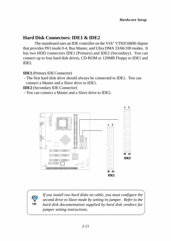
Current CPU Temp., Current System Temp., Current CPU/System Fan Speed,Vcore, 2.5/3.3/5/12VThese items display the current status of all of the monitored hardwaredevices/components such as CPU voltages, temperatures and all fans’sspeed.
PC Health StatusThis section is to monitor the current hardware status including CPUtemperature, CPU Fan speed, Vcore etc. This is available only if there ishardware monitoring onboard.

AWARD® BIOS Setup
3-31
Frequency/Voltage Control
Auto Detect DIMM/PCI ClkThis item is used to auto detect the DIMM/PCI slots. When set to Enabled,the system will remove (turn off) clocks from empty DIMM/PCI slots tominimize the electromagnetic interference (EMI). Settings: Enabled andDisabled.
Spread SpectrumWhen the motherboard clock generator pulses, the extreme values (spikes)of the pulses creates EMI (Electromagnetic Interference). The SpreadSpectrum function reduces the EMI generated by modulating the pulses sothat the spikes of the pulses are reduced to flatter curves. If you do nothave any EMI problem, leave the setting at Disabled for optimal systemstability and performance. But if you are plagued by EMI, setting to En-abled for EMI reduction. Remember to disable Spread Spectrum if you areoverclocking because even a 0.25% jitter can introduce a temporary boost inclockspeed of 25MHz (with a 1GHz CPU) which may just cause youroverclocked processor to lock up.
CPU Host/PCI ClockThis item specifies the combination of CPU host bus (FSB) and PCI busfrequency and provides a method for end users to overclock the processoraccordingly. If the item shows Default, the clock frequency will use thedefault value for both the CPU host bus and PCI bus.

Chapter 3
3-32
The two options on the main menu allow users to restore all of the BIOSsettings to the default Fail-Safe or Optimized values. The Optimized Defaultsare the default values set by the mainboard manufacturer specifically for theoptimal performance of the mainboard. The Fail-Safe Defaults are the defaultvalues set by the BIOS vendor for the stable system performance.
When you select Load Fail-Safe Defaults, a message as below appears:
Pressing Y loads the BIOS default values for the most stable, minimal systemperformance.
Load Fail-Safe/Optimized Defaults

AWARD® BIOS Setup
3-33
When you select Load Optimized Defaults, a message as below appears:
Pressing Y loads the default factory settings for optimal system performance.

Chapter 3
3-34
Set Supervisor/User PasswordWhen you select this function, a message as below will appear on the screen:
Type the password, up to eight characters in length, and press <Enter>. Thepassword typed now will clear any previously set password from CMOSmemory. You will be prompted to confirm the password. Re-type the passwordand press <Enter>. You may also press <Esc> to abort the selection and notenter a password.
To clear a set password, just press <Enter> when you are prompted to enter thepassword. A message will show up confirming the password will be disabled.Once the password is disabled, the system will boot and you can enter Setupwithout entering any password.
When a password has been set, you will be prompted to enter it every time youtry to enter Setup. This prevents an unauthorized person from changing anypart of your system configuration.
Additionally, when a password is enabled, you can also have BIOS to requesta password each time the system is booted. This would prevent unauthorizeduse of your computer. The setting to determine when the password prompt isrequired is the Security Option of the Advanced BIOS Features menu. If theSecurity Option is set to System, the password is required both at boot and atentry to Setup. If set to Setup, password prompt only occurs when trying to

AWARD® BIOS Setup
3-35
enter Setup.
About Supervisor Password & User Password:
Supervisor password : Can enter and change thesettings of the setup menu.
User password: Can only enter but do not havethe right to change the settings ofthe setup menu.

Chapter 3
3-36
Save & Exit SetupWhen you want to quit the Setup menu, you can select this option to save thechanges and quit. A message as below will appear on the screen:
Typing Y will allow you to quit the Setup Utility and save the user setupchanges to RTC CMOS.
Typing N will return to the Setup Utility.

AWARD® BIOS Setup
3-37
Exit Without SavingWhen you want to quit the Setup menu, you can select this option to abandonthe changes. A message as below will appear on the screen:
Typing Y will allow you to quit the Setup Utility without saving any changes toRTC CMOS.
Typing N will return to the Setup Utility.

G-1
Glossary
ACPI (Advanced Configuration & Power Interface)This power management specification enables the OS (operating system) to control theamount of power given to each device attached to the computer. Windows 98/98SE,Windows 2000 and Windows ME can fully support ACPI to allow users managing thesystem power flexibly.
AGP (Accelerated Graphics Port)A new, high-speed graphics interface that based on PCI construction and designedespecially for the throughput demands of 3-D graphics. AGP provides a direct channel(32-bit wide bus) between the display controller and main memory for high graphicsquality and performance.
ATXA modern shape and layout of mainboard that supersedes the widely-used Baby ATform factor. It improves many placement of components and makes a more efficientdesign.
BIOS (basic input/output system)On PCs, an essential software that contains all the control code of input/output inter-face (such as keyboard, disk drives, etc.). It executes hardware test on booting thesystem, starts the OS, and provides an interface between the OS and the components.The BIOS is stored in a ROM chip.
BusA set of hardware lines within the computer system, through which the data is trans-ferred among different components. In a PC, the term bus usually refers to a local busthat connects the internal components to the CPU and main memory.
CacheA special memory subsystem that is used to speed up the data transfer. It stores thecontents of frequently accessed RAM locations and the addresses where these dataitems are stored.
ChipsetA collection of integrated chips designed to perform one or more related functions. For
GlossaryGlossary

G-2
Glossary
Dynamic RAM (DRAM) Memory Technologies Type
FPM (60,70ns)EDO (50,60,70ns)SDRAM (66MHz)SDRAM (100MHz)SDRAM (133MHz)RDRAM (Direct Rambus)DDR SDRAM (100MHz)DDR SDRAM (133MHz)
First Used
1990 1994 1996 1998 1999 1999 2000 2000
Clock Rate
25MHz 40MHz 66MHz 100MHz 133MHz 400MHz 100MHz 133MHz
Bus* Width
64 bits 64 bits 64 bits 64 bits 64 bits 16 bits 64 bits 64 bits
Bandwidth 200 MBps 320 MBps 528 MBps 800 MBps 1.1 GBps 1.6 GBps 1.6 GBps 2.1 GBps
Volts
5v 5v 3.3v 3.3v 3.3v 2.5v 3.3v 3.3v
Peak
* Memory channel width (64 bits started with 75MHz Pentium)
Source: Computer Desktop Encyclopedia
example, a modem chipset contains all the primary circuits for transmitting and receiv-ing data; a PC chipset provides the electronic interfaces between all subsystems.
CMOS (complementary metal-oxide semiconductor)CMOS is a widely used type of semiconductor, which features high speed and lowpower consumption. PCs usually contain a small amount of battery-powered CMOSmemory to retain the date, time, and system setup parameters.
COMIn MS-DOS system, the name of a serial communications port. DOS supports fourserial ports. For example, if a modem is connected to one serial port and a serial mouseto another, they are identified as COM1 and COM2.
DIMM (dual in-line memory module)A small circuit board that holds memory chips. A SIMM (single in-line memorymodule) has a 32-bit path to the memory chips whereas a DIMM has 64-bit path.
DRAM (Dynamic RAM)A most common type of computer memory. It usually uses one transistor and acapacitor to represent a bit. As the development of technology, the memory type andspecification used in computer becomes variety, such as SDRAM, DDR SDRAM, andRDRAM. For further instruction, please see the table below:

G-3
Glossary
ECC Memory (error correcting code memory)A type of memory that contains special circuitry for testing the accuracy of data andcorrecting the errors on the fly.
IDE (Integrated Drive Electronics)A type of disk-drive interface widely used to connect hard disks, CD-ROMs and tapedrives to a PC, in which the controller electronics is integrated into the drive itself,eliminating the need for a separate adapter card. The IDE interface is known as theATA (AT Attachment) specification.
IEEE 1394A new, high speed external bus standard, also known as FireWire or iLink, whichsupports data transfer rates of up to 400 Mbps for connecting up to 63 externaldevices.
IrDA (Infrared Data Association)A group of device vendors, including computer, component and telecommunications,who have developed a standard for transmitting data via infrared light waves. Thisenables you to transfer data from one device to another without any cables.
LAN (local area network)A computer network that covers a relatively smaller area, such as in a building or anenterprise. It is made up of servers, workstations, shared resources, a network oper-ating system and a communications link. These individual PCs and devices on a LANare known as “nodes”, and are connected by cables to access data and devices any-where on the LAN, so that many users can share expensive devices and data.
LED (light emitting diode)A semiconductor device that converts electrical energy into light. Since it lights up(usually red) when electricity is passed through it, it is usually used for the activitylights on computer’s component, such as disk drivers.
LPT (line printer terminal)Logical device name for a line printer; a name reserved by the MS-DOS for up to threeparallel printer ports: LPT1, LPT2, and LPT3. It is frequently used by the OS toidentify a printer.

G-4
Glossary
PCI (Peripheral Component Interconnect)A local bus standard developed by Intel that first appeared on PCs in late 1993. PCIprovides “plug and play” capability and allows IRQs to be shared. The PCI controllercan exchange data with the system's CPU either 32 bits or 64 bits at a time.
PnP (Plug and Play)A set of specifications that allows a PC to configure itself automatically to work withperipherals. The user can "plug" in a peripheral device and "play" it without configur-ing the system manually. To implement this useful feature, both the BIOS that sup-ports PnP and a PnP expansion card are required.
POST (Power On Self Test)During booting up your system, the BIOS executes a series of diagnostic tests, includechecking the RAM, the keyboard, the disk drives, etc., to see if they are properlyconnected and operating.
PS/2 PortA type of port developed by IBM for connecting a mouse or keyboard to a PC. ThePS/2 port supports a mini DIN plug containing just 6 pins. Most modern PCs equippedwith PS/2 ports so that the special port can be used by another device, such as amodem.
USB (universal serial bus)A hardware interface for low-speed peripherals such as the keyboard, mouse, joystick,etc. USB provides a maximum bandwidth of 12 Mbit/sec (Mbps) for connecting up to127 peripheral devices to PC. USB features hot swap capability and multiple datastreams, allows external devices to be plugged in and unplugged without turning thesystem off.
VirusA program or a piece of code that infects computer files by inserting in those filescopies of itself. The virus code is buried within an existing program, and is activatedwhen that program is executed. All the viruses are man-made, and often have damagingside effects.